True-Hspice Device Models Reference Manual, Release 2001.4, revision A 7-1 Chapter 7 Using IBIS Models The Input/Output Buffer Information Specification (IBIS) is being developed by the IBIS Open Forum, which is affiliated with the Electronic Industries Alliance (EIA). IBIS specifies a standard form for presentation of information in ASCII format in special files. This information describes behavior of various I/O buffers that send electrical signals outside the silicon chip or receive such signals. The type of information includes output I-V curves for output buffers in LOW and HIGH states, V(t) curves describing the exact form of transitions from LOW to HIGH states and from HIGH to LOW states for a given load, values for die capacitance, electrical parameters of the packages, and so on. The IBIS standard specifies only the “form” of information, and does not specify how the information should be processed or used by the simulator. However, the IBIS standard contains a section devoted to recommendations on how information should be derived through the simulation or from the silicon measurement. In addition, the IBIS Open Forum has sponsored development of a parser for IBIS files—called the golden parser. The golden parser is freely available as an executable and should be used for verification of IBIS files. The golden parser is incorporated into Avant! in-circuit simulators. When the golden parser processes an IBIS file, it produces warnings and/or error messages which by default appear in the Hspice output. The I/O buffer element type is called buffer. The name of this element starts with the letter b. Using buffers is similar to using other simulation elements, such as transistors: give a name to the buffer, specify a list of nodes that are used to connect the buffer to the rest of the circuit, and specify parameters. Only parameters that specify a model for the buffer (file name and model name) are required.
Transcript
True-Hspice Device Models Reference Manual, Release 2001.4, revision A 7-1
Chapter 7
Using IBIS Models
The Input/Output Buffer Information Specification (IBIS) is being developed bythe IBIS Open Forum, which is affiliated with the Electronic Industries Alliance(EIA). IBIS specifies a standard form for presentation of information in ASCIIformat in special files. This information describes behavior of various I/Obuffers that send electrical signals outside the silicon chip or receive suchsignals. The type of information includes output I-V curves for output buffers inLOW and HIGH states, V(t) curves describing the exact form of transitions fromLOW to HIGH states and from HIGH to LOW states for a given load, values fordie capacitance, electrical parameters of the packages, and so on. The IBISstandard specifies only the “form” of information, and does not specify how theinformation should be processed or used by the simulator.
However, the IBIS standard contains a section devoted to recommendations onhow information should be derived through the simulation or from the siliconmeasurement. In addition, the IBIS Open Forum has sponsored development ofa parser for IBIS files—called the golden parser. The golden parser is freelyavailable as an executable and should be used for verification of IBIS files. Thegolden parser is incorporated into Avant! in-circuit simulators. When the goldenparser processes an IBIS file, it produces warnings and/or error messages whichby default appear in the Hspice output.
The I/O buffer element type is called buffer. The name of this element starts withthe letter b. Using buffers is similar to using other simulation elements, such astransistors: give a name to the buffer, specify a list of nodes that are used toconnect the buffer to the rest of the circuit, and specify parameters. Onlyparameters that specify a model for the buffer (file name and model name) arerequired.
Using IBIS Models
7-2 True-Hspice Device Models Reference Manual, Release 2001.4, revision A
Two significant differences from the use of other elements are:
1. The number of external nodes is variable depending on the buffer type andcan be from 4 to 8; and
2. Nodes that are suppose to connect to power/ground rails must not beconnected in the netlist, because simulation does this connection bydefault.
This chapter is not intended to introduce the IBIS standard, because it is a largedocument; familiarity with the standard is assumed. A significant amount ofinformation is available on the Internet, and appropriate links to other sites arelisted in “References” on page 7-56.
Three types of analysis are supported for input/output buffers:■ DC analysis■ Transient analysis■ AC analysis
This chapter covers the following topics:■ IBIS Conventions■ Buffers■ Specifying Common Keywords■ Differential Pins■ Scaling Buffer Strength■ Example■ Using the IBIS Buffer Component■ Additional Notes■ Warning and Error Messages■ References
Using IBIS Models IBIS Conventions
True-Hspice Device Models Reference Manual, Release 2001.4, revision A 7-3
IBIS ConventionsThe general syntax of an element card for I/O buffers is:
General Form:bname node_1 node_2 ... node_N+ keyword_1=value_1 ... [keyword_M=value_M]
where:
Figure 7-1: Circuit Diagram for Package
bname Buffer element name. Must begin with B, whichcan be followed by up to 1023 alphanumericcharacters.
node_1 node_2 ...node_N
List of I/O buffer external nodes. The number ofnodes and corresponding rules are specific todifferent buffer types (see later sections in thischapter).
keyword_i=value_i Assigns value, value_i, to the keyword,keyword_i. Optional keywords are given insquare brackets (see “Specifying CommonKeywords” on page 7-27 for more information).
node_p
C_p
node_p
R_p
node_o
L_p
gnd
General Form: Using IBIS Models
7-4 True-Hspice Device Models Reference Manual, Release 2001.4, revision A
The gnd node on the circuit diagram for buffers denotes the ideal SPICE groundnode (the notation node 0 [zero] is also used). This node is always available inthe simulation device models. Do not include this node in the node list on thebuffer card. If the gnd node appears on a circuit diagram, simulation makes thenode connection to the ideal ground. Node gnd is used on circuit diagrams toexplain the connection of individual parts inside buffers.
In some cases, buffer nodes have different rules than nodes for other elements.Some nodes may already be connected to voltage sources (simulation makessuch connections) so it is incorrect to connect a voltage source to such nodes.Conversely, some nodes should be connected to voltage sources and it isincorrect not to connect voltage sources to these nodes.
Note: See “Specifying Common Keywords” on page 7-27, and the sectionsabout individual buffer types, for detailed explanations of how to usethese nodes.
Buffers correspond to models in IBIS files and do not include packages. At thistime, corresponding packages should be added manually. For example, ifnode_out and node_pin are nodes for output of the output buffer andcorresponding pin, then add the following lines to the netlist:
where values for R_pkg, L_pkg, and C_pkg are taken from the IBIS file (seeFigure 7-1 on page 7-3 for the circuit diagram).
Using IBIS Models Terminology
True-Hspice Device Models Reference Manual, Release 2001.4, revision A 7-5
TerminologyThe following are definitions of terms used frequently in this chapter:
Limitations and RestrictionsThe series, series switch, and terminator buffers are not implemented.
You can simulate the terminator by using other existing elements: resistors,capacitors, and voltage dependent current sources.
card, buffer card Used to denote a line(s) from the netlist thatspecifies the buffer name (should begin with theletter b), a list of external nodes, required keyword,and optional keywords.
buffer, I/O buffer,input/output buffer
One of 14 IBIS models as specified in the standard,version 3.2, and implemented in the Avant!simulation device models.
RWF, FWF Rising waveform, falling waveform
I/O Input/Output
I/V curve Current-voltage curve
PU, PD Pullup, pulldown
PC, GC Power clamp, ground clamp
Buffers Using IBIS Models
7-6 True-Hspice Device Models Reference Manual, Release 2001.4, revision A
BuffersThis section describes the buffers as implemented in Avant! simulation devicemodels. Please refer to “Specifying Common Keywords” on page 7-27 fordetails on using keywords shown in the syntax examples in the followingsections.
Input BufferThe syntax of an input buffer element card is:
where the total number of external nodes is equal to 4.
If keyword power=on (default) is specified, nodes nd_pc and nd_gc areconnected to voltage sources with values taken from the IBIS file. You shouldnot connect these nodes to voltage sources. However, names for these nodesshould be provided, so you can print out the voltage values if required. Forexample:
.PRINT V(nd_pc) V(nd_gc)
If you specify the power=off keyword, simulation does not connect these nodesto voltage sources. You should connect the nodes to voltage sources eitherdirectly or through an RLC network, or a transmission line.
Using IBIS Models Input Buffer
True-Hspice Device Models Reference Manual, Release 2001.4, revision A 7-7
There are no special rules for node_in and node_in can connect to I, E, F, G, andH elements. The buffer measures and processes the voltage on this node andsends a response to node nd_out_of_in. The node nd_out_of_in is connected tothe voltage source as shown in Figure 7-2. It is an error to connect this node to avoltage source. If power=off, nodes nd_pc, nd_gc can be connected to theground is the intention is to specify voltage zero on these nodes.
Figure 7-2: Input Buffer
V_out_of_in is a digital signal that assumes values of either 0 or 1 depending onthe voltages V_in, Vinh, Vinl, and Polarity. Simulation processes V_out_of_inaccording to the following rules.
nd_pc
nd_i
C_co
gndnd_gc
V_in1M
nd_out_of_
V_out_of
gn
PC
GC
Output Buffer Using IBIS Models
7-8 True-Hspice Device Models Reference Manual, Release 2001.4, revision A
Figure 7-2 on page 7-7 shows a single circuit specified on a single element card.V_out_of_in is a voltage source whose value is a function of V_in (as well as ofthresholds Vinl, Vinh, and parameter Polarity). It can be used to drive othercircuits.
If pc_scal or gc_scal arguments exist and pc_scal_value or gc_scal_value do notequal 1.0, then PC or GC iv curve will be adjusted using the pc_scal_value orgc_scal_value.
Output BufferThe syntax for an output buffer element card is:
The nd_pc and nd_gc nodes are optional. However, either both or none can bespecified. The total number of external nodes is either 4 or 6, any other numberis an error. If you do not specify the nd_pc and nd_gc nodes on the element card,but Power_Clamp and/or Ground_Clamp I-V curves are present in the model inquestion, then the simulator simply connects Power_Clamp and/orGround_Clamp to the corresponding nd_pu (pullup) and/or nd_pd (pulldown).
However, the optional nodes nd_pc and nd_gc are needed if:■ IBIS keywords POWER Clamp Reference and GND Clamp Reference are
present in the IBIS model and have different values than the IBIS keywordsPullup Reference and Pulldown Reference, or
■ IBIS keywords Pullup Reference and Pulldown Reference do not exist andPOWER Clamp Reference and GND Clamp Reference have different valuesthan those determined by the Voltage Range IBIS keyword.
If optional nodes nd_pc and nd_gc are needed, but omitted from the elementcard, simulation issues a warning and connects nd_pc to nd_pu and nd_gc tond_pd.
Output Buffer Using IBIS Models
7-10 True-Hspice Device Models Reference Manual, Release 2001.4, revision A
Figure 7-3: Output Buffer
If keyword power=on (default) is specified, nodes nd_pu, nd_pd, and ifspecified, nd_pc and nd_gc, are connected to voltage sources with values takenfrom the IBIS file. You should not connect these nodes to voltage sources.However, names for these nodes should be provided, so you can print out thevoltage values if required. For example:
.PRINT V(nd_pu) V(nd_pd)
If you specify the power=off keyword, simulation does not connect these nodesto voltage sources. You should connect the nodes to voltage sources eitherdirectly or through an RLC network or a transmission line.
There are no special rules for node nd_out. The voltage on this node is controlledby the digital signal on the node nd_in. Now any voltage source, current source,voltage controlled voltage source, voltage controlled current source, currentcontrolled voltage source, or current controlled current source can be connectedto the nd_in as shown in the following example:
If power=off, nodes nd_pu, nd_pd, nd_pc, nd_gc can be connected to the groundif the intention is to have zero voltage on these nodes.
nd_pu
nd_
C_co
gndnd_pd
V_out
nd_pc
nd_gc
I_out
P
P
P
G
V_in
Using IBIS Models Output Buffer
True-Hspice Device Models Reference Manual, Release 2001.4, revision A 7-11
V_in is a controlling signal representing a digital signal with values 0 and 1.However, simulation can use any signal and process, according to the followingrules:
If pc_scal (or gc_scal, pu_scal, pd_scal) argument exists and pc_scal_value (orgc_scal_value, pu_scal_value, pd_scal_value) does not equal to 1.0, the PC (orGC, PU, PD) iv curve will be adjusted using the pc_scal_value (orgc_scal_value, pu_scal_value, pd_scal_value).
If rwf_scal (or fwf_scal) argument exists and rwf_scal_value (orfwf_scal_value) does not equal to 1.0, rising and falling vt curves will beadjusted using rwf_scal_value (or fwf_scal_value).
If spu_scal (or spd_scal) argument exists and spu_scal_value (orspd_scal_value) does not equal to 0.0, but at the same time power is equal to offand (spu_scal_value-spd_scal_value) does not equal to the corresponding valuein the .ibs file, then the iv curves of PU (or PD) will be adjusted usingspu_scal_value (or spd_scal_value).
If:
Polarity=Non-Inverting
At t=0 for transient analysis (or for DCanalysis), the buffer goes to HIGH state if V_in> 0.5 and to LOW in the opposite case.
Next, if the buffer is in HIGH state, it will go toLOW state if V_in < 0.2. If the buffer is in LOWstate, it will go to HIGH state if V_in > 0.8.
Polarity=Inverting At t=0 for transient analysis (or for DCanalysis), the buffer goes to HIGH state if V_in< 0.5 and to LOW in the opposite case.
Next, if the buffer is in HIGH state, it will go toLOW state if V_in > 0.8. If the buffer is in LOWstate, it will go to HIGH state if V_in < 0.2.
Tristate Buffer Using IBIS Models
7-12 True-Hspice Device Models Reference Manual, Release 2001.4, revision A
Tristate BufferThe syntax for a tristate buffer element card is:
The nd_pc and nd_gc nodes are optional. However, either both or none can bespecified. The total number of external nodes is either 5 or 7; any other numberis an error. If nodes nd_pc and nd_gc are not given on the element card butPower_Clamp and/or Ground_Clamp I-V curves are present in the model inquestion, then the simulator will simply add Power_Clamp and/orGround_Clamp I-V curves data to corresponding Pull_Up and/or Pull_DownI-V curves data.
However, the optional nodes nd_pc and nd_gc are needed if:■ IBIS keywords POWER Clamp Reference and GND Clamp Reference are
present in the IBIS model and have different values than the IBIS keywordsPullup Reference and Pulldown Reference, or
■ IBIS keywords Pullup Reference and Pulldown Reference do not exist andPOWER Clamp Reference and GND Clamp Reference have different valuesthan those determined by the Voltage Range IBIS keyword.
Using IBIS Models Tristate Buffer
True-Hspice Device Models Reference Manual, Release 2001.4, revision A 7-13
If optional nodes nd_pc and nd_gc are needed, but omitted from the elementcard, simulation issues a warning and connects nd_pc to nd_pu and nd_gc tond_pd.
Figure 7-4: Tristate Buffer
If you specify the power=on (default) keyword, then the nd_pu, nd_pd nodes,and if specified, nd_pc and nd_gc, are connected to voltage sources with valuestaken from the IBIS file. You should not connect these nodes to voltage sources.
However, names for these nodes should be provided in the netlist, so you canprint out the voltage values if required. For example:
.PRINT V(nd_pu) V(nd_pd)
If you specify the power=off keyword, simulation does not connect these nodesto voltage sources. You should connect the nodes to voltage sources eitherdirectly or through an RLC network, or a transmission line.
There are no special rules for nd_out. The voltage on this node is controlled bythe digital signal on the nodes nd_in, nd_en. Voltage sources must be connectedto the nodes nd_in, nd_en as shown in the following example:
7-14 True-Hspice Device Models Reference Manual, Release 2001.4, revision A
The nd_pu, nd_pd, nd_pc, and nd_gc nodes can be connected to the ground ifthe intention is to have zero voltage on these nodes. Nodes nd_in, nd_en can notbe connected to the ground.
V_in and V_en are controlling signals representing digital signals with values 0and 1. Simulation can use any signal and process according to the followingrules:
Using IBIS Models Tristate Buffer
True-Hspice Device Models Reference Manual, Release 2001.4, revision A 7-15
The enable signal, V_en, supersedes the input signal, V_in.If:
ENABLE = Active-High At t=0 for transient analysis (or for DC analysis),the buffer goes to the ENABLE state if V_en > 0.5and to DISABLE in the opposite case.
ENABLE = Active-Low At t=0 for transient analysis (or for DC analysis),the buffer goes to ENABLE state if V_en < 0.5 andto DISABLE in the opposite case.
The buffer is in ENABLEstate
Begins transition to DISABLE state if V_en < 0.2(where Enable = Active-High) and if V_en > 0.8(where Enable = Active-Low).
The buffer is in DISABLE
state or in the process oftransition from ENABLE
state to DISABLE state
Begins transition to ENABLE state if V_en > 0.8(where Enable = Active-High) and if V_en < 0.2(where Enable = Active-Low).
The buffer is in ENABLE
stateResponse to the input signal, V_in, is the same asthe output buffer.
Polarity=Non-Inverting At t=0 for transient analysis (or for DC analysis),the buffer goes to HIGH state if V_in > 0.5 and toLOW in the opposite case.
Next, if the buffer is in HIGH state, it will go toLOW state if V_in < 0.2. If the buffer is in LOWstate, it will go to HIGH state if V_in > 0.8.
Polarity=Inverting At t=0 for transient analysis (or for DC analysis),the buffer goes to HIGH state if V_in < 0.5 and toLOW in the opposite case.
Next, if the buffer is in HIGH state, it will go toLOW state if V_in > 0.8. If the buffer is in LOW
state, it will go to HIGH state if V_in < 0.2.
Input/Output Buffer Using IBIS Models
7-16 True-Hspice Device Models Reference Manual, Release 2001.4, revision A
Note: After the buffer begins a transition from ENABLE state to DISABLEstate, all memory about previous HIGH/LOW states is lost. If the bufferlater goes to the ENABLE state, it compares the controlling signal,V_in, against the threshold 0.5 to decide whether to go to HIGH stateor LOW state similar to the time moment t=0, rather than against thethresholds 0.2 and 0.8.
Input/Output BufferThe syntax of an input/output buffer element card is:
True-Hspice Device Models Reference Manual, Release 2001.4, revision A 7-17
The nd_pc and nd_gc nodes are optional. However, either both or none can bespecified. The total number of external nodes is either 6 or 8; any other numberis an error. If nodes nd_pc and nd_gc are not given on the element card butPower_Clamp and/or Ground_Clamp I-V curves are present in the model inquestion, then the simulator will simply add Power_Clamp and/orGround_Clamp I-V curves data to corresponding Pull_Up and/or Pull_Down I-V curves data.
However, the optional nodes nd_pc and nd_gc are needed if:■ IBIS keywords POWER Clamp Reference and GND Clamp Reference are
present in the IBIS model and have different values than the IBIS keywordsPullup Reference and Pulldown Reference, or
■ IBIS keywords Pullup Reference and Pulldown Reference do not exist andPOWER Clamp Reference and GND Clamp Reference have different valuesthan those determined by the Voltage Range IBIS keyword.
If you need the nd_pc and nd_gc optional nodes, but you omitted them from theelement card, simulation issues a warning and connects nd_pc to nd_pu andnd_gc to nd_pd.
Input/Output Buffer Using IBIS Models
7-18 True-Hspice Device Models Reference Manual, Release 2001.4, revision A
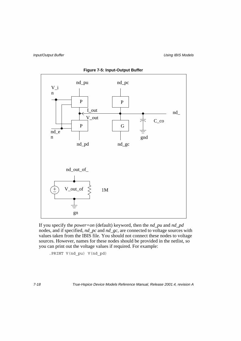
Figure 7-5: Input-Output Buffer
If you specify the power=on (default) keyword, then the nd_pu and nd_pdnodes, and if specified, nd_pc and nd_gc, are connected to voltage sources withvalues taken from the IBIS file. You should not connect these nodes to voltagesources. However, names for these nodes should be provided in the netlist, soyou can print out the voltage values if required. For example:
.PRINT V(nd_pu) V(nd_pd)
nd_pu
nd_
C_co
gndnd_pd
V_out
nd_pc
nd_gc
I_out
P
P
P
G
V_in
nd_en
1M
nd_out_of_
V_out_of
gn
Using IBIS Models Input/Output Buffer
True-Hspice Device Models Reference Manual, Release 2001.4, revision A 7-19
If you specify the power=off keyword, simulation does not connect these nodesto voltage sources. You should connect the nodes to voltage sources eitherdirectly or through an RLC network or a transmission line.
There are no special rules for node nd_out. The voltage on this node is controlledby the digital signal on the nodes nd_in, nd_en. Voltage sources must beconnected to the nodes nd_in, nd_en as shown in the following example:
The nd_pu, nd_pd, nd_pc, and nd_gc nodes can be connected to the ground ifthe intention is to have zero voltage on these nodes.
The nd_out_of_in node is connected to a voltage source (see Figure ). It is anerror to connect this node to a voltage source or the ground.
The input-output buffer is a combination of the tristate buffer and the inputbuffer. See “Input Buffer” on page 7-6 and “Tristate Buffer” on page 7-12 formore information.
The input-output buffer can function as an input buffer. In this case, the resultantdigital signal V_out_of_in on the node nd_out_of_in is controlled by the voltageV_out on the node nd_out.
For the input buffer, this controlling voltage is called V_in and anycorresponding node is nd_in.
The input-output buffer uses V_in, nd_in notations to denote the controllingvoltage and controlling input node for the output part of the buffer.
If the input-output buffer is not in the DISABLE state (this includes ENABLEstate and transitions to ENABLE->DISABLE and DISABLE->ENABLE), thenit functions as a tristate buffer. If input-output buffer is in the DISABLE state, itfunctions as an input buffer.
However, there is a difference in the digital output of the input part of the buffer(voltage V_out_of_in). Because V_out_of_in is not always defined (e.g. thebuffer is in ENABLE state, or Vinl < V_out < Vinh at the time moment, whenthe transition to DISABLE state is completed) and because we want to preservelogical LEVELs 0 and 1 for LOW and HIGH states, V_out_of_in takes the value0.5 when it is undefined.
Open Drain, Open Sink, Open Source Buffers Using IBIS Models
7-20 True-Hspice Device Models Reference Manual, Release 2001.4, revision A
Figure 7-5 on page 7-18 shows a single circuit specified on a single elementcard. The V_out_of_in is a voltage source whose value is a function of V_out (aswell as of thresholds Vinl, Vinh and parameter Polarity). It can be used to driveother circuits.
Open Drain, Open Sink, Open Source BuffersOpen drain and open sink buffers do not have pullup circuitry. Open sourcebuffers do not have pulldown circuitry. However, the element cards for thesethree buffers coincide with the element card for the output buffer. Accordingly,you should always specify names for pullup and pulldown nodes, nd_pu andnd_pd, even if the buffer does not have pullup or pulldown circuitry.
All rules given in “Output Buffer” on page 7-8 apply to open drain, open sink,and open source buffers with the following exceptions:
■ Because open drain and open sink buffers do not have pullup circuitry, theoption xv_pu=nd_state_pu should not be specified.
■ Similarly, because open source buffers do not have pulldown circuitry, theoption xv_pd=nd_state_pd should not be specified.
I/O Open Drain, I/O Open Sink, I/O OpenSource BuffersI/O open drain and I/O open sink buffers do not have pullup circuitry. I/O opensource buffers do not have pulldown circuitry. However, the element cards forthese three buffers coincide with the element card for the input-output buffer.Accordingly, you should always specify names for pullup and pulldown nodes,nd_pu and nd_pd, even if the buffer does not have pullup or pulldown circuitry.
All rules given in “Input/Output Buffer” on page 7-16 are applicable to I/O opendrain, I/O open sink, and I/O open source buffers with the following exceptions:
■ Because I/O open drain and I/O open sink buffers do not have pullupcircuitry, the option xv_pu=nd_state_pu should not be specified.
■ Similarly, because I/O open source buffers do not have pulldown circuitry,the option xv_pd=nd_state_pd should not be specified.
Using IBIS Models Input ECL Buffer
True-Hspice Device Models Reference Manual, Release 2001.4, revision A 7-21
Input ECL BufferThe syntax of the input ECL buffer element card is:
Nodes nd_pc and nd_gc are optional. However, either both or none can bespecified. The total number of external nodes is either 3 or 5, any other numberis an error. The output ECL buffer does not have a pulldown node. The pulldowntable in the IBIS file is referenced in respect to pullup voltage.
If nodes nd_pc and nd_gc are not given on the element card but Power_Clampand/or Ground_Clamp I-V curves are present in the model in question, then thesimulator will issue an error message (this simulator behavior is different fromthat for the output buffer).
In other respects, the output ECL buffer is similar to the output buffer. For moreinformation, see “Output Buffer” on page 7-8.
Using IBIS Models Tristate ECL Buffer
True-Hspice Device Models Reference Manual, Release 2001.4, revision A 7-23
Figure 7-7: Output ECL Buffer
Tristate ECL BufferThe syntax for the tristate ECL buffer element card is:
7-24 True-Hspice Device Models Reference Manual, Release 2001.4, revision A
The nd_pc and nd_gc nodes are optional. However, either both or none can bespecified. The total number of external nodes is either 4 or 6, any other numberis an error. The tristate ECL buffer does not have a pulldown node. Thepulldown table in the IBIS file is referenced in respect to pullup voltage.
If nodes nd_pc and nd_gc are not given on the element card but Power_Clampand/or Ground_Clamp I-V curves are present in the model in question, then thesimulator will issue an error message (this simulator behavior is different fromthat for the tristate buffer).
In other respects, the tristate ECL buffer is similar to the tristate buffer. See“Tristate Buffer” on page 7-12 for more information.
Figure 7-8: Tristate ECL Buffer
nd_pu
nd_
C_co
gnd
V_out
nd_pc
nd_gc
I_out
P
P
P
G
V_in
nd_en
Using IBIS Models Input-Output ECL Buffer
True-Hspice Device Models Reference Manual, Release 2001.4, revision A 7-25
Input-Output ECL BufferThe syntax for the input-output ECL buffer element card is:
Nodes nd_pc and nd_gc are optional. However, either both or none can bespecified. The total number of external nodes is either 5 or 7, any other numberis an error. The tristate ECL buffer does not have a pulldown node. Thepulldown table in the IBIS file is referenced in respect to pullup voltage.
If nodes nd_pc and nd_gc are not given on the element card but Power_Clampand/or Ground_Clamp I-V curves are present in the model in question, then thesimulator will issue an error message (this simulator behavior is different fromthat for Input-Output buffer).
In other respects, the input-output ECL buffer is similar to the input-outputbuffer. See “Input/Output Buffer” on page 7-16 for more information.
Input-Output ECL Buffer Using IBIS Models
7-26 True-Hspice Device Models Reference Manual, Release 2001.4, revision A
Figure 7-9: Input-Output ECL Buffer
nd_pu
nd_
C_co
gnd
V_out
nd_pc
nd_gc
I_out
P
P
P
G
V_in
nd_en
1M
nd_out_of_
V_out_of
gn
Using IBIS Models Specifying Common Keywords
True-Hspice Device Models Reference Manual, Release 2001.4, revision A 7-27
Specifying Common Keywords
Required Keywords
file='file_name'Identifies the IBIS file. file_name must be lower case and specify either theabsolute path for the file or the relative path in respect to the directory fromwhich you run the simulator.
model='model_name'Identifies the model for a buffer from the IBIS file, specified with keywordfile='...'. The keyword model_name is case sensitive and must match one of themodels from the IBIS file.
Optional KeywordsAll other keywords are optional; if not used, default values will be selected.Optional keywords are enclosed in square brackets [ ] in the buffer cards.
The notation keyword={val_1|val_2|...|val_n} is used to denote that the keywordtakes a value from the set val_1, val_2, ... , val_n. The order of the keywords isnot important.
Optional Keywords Using IBIS Models
7-28 True-Hspice Device Models Reference Manual, Release 2001.4, revision A
buffer= {Buffer_Number | Buffer_Type}Where buffer_number is an integer from the range 1 ≤ N ≤ 17. Each buffer hasan assigned number as follows:
Buffer Type Buffer NumberNumber of nodes(nominal or min/max)
Notes
INPUT 1 4
OUTPUT 2 4/6
INPUT_OUTPUT 3 6/8
THREE_STATE 4 5/7
OPEN_DRAIN 5 4/6
IO_OPEN_DRAIN 6 6/8
OPEN_SINK 7 4/6
IO_OPEN_SINK 8 6/8
OPEN_SOURCE 9 4/6
IO_OPEN_SOURCE
10 6/8
INPUT_ECL 11 4
OUTPUT_ECL 12 3/5
IO_ECL 13 5/7
THREE_STATE_ECL
14 4/6 was 17
SERIES 15 not implemented
SERIES_SWITCH 16 not implemented
TERMINATOR 17 not implemented was 14
Using IBIS Models Optional Keywords
True-Hspice Device Models Reference Manual, Release 2001.4, revision A 7-29
The value of buffer_number and buffer_type should match the buffer typespecified by keyword model='...'. The keyword buffer= {Buffer_Number |Buffer_Type} provides an extra check for the input netlist. If the keyword isomitted, this checking is not performed.
typ={typ|min|max|fast|slow}If the value of the buffer parameter typ is either typ, or min, or max, then thisvalue signifies the column in the IBIS file from which the data are used for thecurrent simulation. The default is typ=typ. If min or max data are not available,typ data are used instead.
If the value of the buffer parameter typ is fast or slow, then certain combinationsof min and max data are used. The following table specifies the exact type of dataused for fast and slow values. Note that the table lists all the parameters and datatypes for all implemented buffers. Specific buffers use relevant data only. Nobuffer uses all the data given in the table (for example, the Rgnd, Rpower, Rac,Cac parameters are specified and used only for the terminator).
hsp_ver=hspice_versionThe default is the current version of the Star-Hspice simulator. If you prefer theprevious version of the IBIS buffer, then you can use the following statement:
hsp_ver = 2001.2
Optional Keywords Using IBIS Models
7-30 True-Hspice Device Models Reference Manual, Release 2001.4, revision A
Parameter/Data Fast Slow
C_comp min max
Temp_Range max min
Voltage_Range max min
Pullup_Ref max min
Pulldown_Ref min max
POWER_Clamp_Ref max min
GND_Clamp_Ref min max
Rgnd max min
Rpower max min
Rac max min
Cac min max
Pulldown max min
Pullup max min
GND_ Clamp max min
POWER_Clamp max min
Ramp max min
Rising_waveform max min
Falling_waveform max min
V_fixture max min
Using IBIS Models Optional Keywords
True-Hspice Device Models Reference Manual, Release 2001.4, revision A 7-31
power={on|off}Default is power=on. Connect buffers to power sources that are specified in theIBIS file with keywords Voltage Range, Pullup Reference, Pulldown Reference,POWER Clamp Reference, and GND Clamp Reference.
By default, simulation connects required voltage sources for such external nodesas Pullup, Pulldown, Power_Clamp, and Ground_Clamp if applicable. Youshould not connect these nodes to voltage sources. However, names for thesenodes should be provided, so you can print out the voltage values if required. Forexample:
.PRINT V(node_pullup)
If power=off is used, then the internal voltage sources are not included in thebuffer and you are responsible for adding external voltage sources. Use thisoption if the voltage source is not connected directly to buffer nodes but througha circuit to account for parasitic RLC, to simulate power/ground bounce, and soon.
interpol={1|2}Default is interpol=1 (recommended). The I/V curves and V(t) curves need tobe interpolated. Keyword interpol=1 uses linear interpolation and interpol=2uses quadratic bi-spline interpolation.
xv_pu=nd_state_puxv_pd=nd_state_pdThe buffers with output function (output, input-output, tristate, and so on) arecontrolled by one (input) or two (input and enable) controlling signals. Describethe state of a buffer at any moment with two state variables, St_pu and St_pd,which vary from 0 to 1. For example, if the output buffer is in LOW state, thenSt_pu=0, St_pd=1. If the output buffer transitions from a LOW state to HIGHstate, then St_pu continuously changes from 0 to 1, while St_pd goes from 1 to0. The actual time dependence for such a transition is derived from either rampdata or waveform(s).
Optional Keywords Using IBIS Models
7-32 True-Hspice Device Models Reference Manual, Release 2001.4, revision A
You might want to know exactly how the transition takes place. The keywordsxv_pu=nd_state_pu, xv_pd=nd_state_pd provide such information. Herend_state_pu and nd_state_pd are names of additional nodes (which must beunique, and are treated as any other node from the netlist, except for a 16-character limitation). If the keyword(s) are included, then simulation addsvoltage source(s) (with 1MOhm parallel resistor).
The values of the voltages are equal to St_pu and St_pd. They can be printed ordisplayed as follows:
.PRINT V(nd_state_pu) V(nd_state_pd)].
Figure 7-10: Equivalent Circuit for xv_pu=nd_state_pu Keyword
ramp_fwf={0|1|2}ramp_rwf={0|1|2}Default is ramp_fwf=0, ramp_rwf=0. If ramp and/or waveform(s) data areavailable, then these options allow you to choose which data to use.
The ramp_fwf parameter controls falling waveform(s)/ramp. The ramp_rwfparameter controls rising waveform(s)/ramp.
1M
nd_state_p
St_p
gn
Using IBIS Models Optional Keywords
True-Hspice Device Models Reference Manual, Release 2001.4, revision A 7-33
■ Value 0 denotes use ramp data.■ Value 1 denotes use one waveform:
❑ For ramp_fwf=1, if more than one falling waveform is available, the firstfalling waveform found for the model in question will be used.
❑ For ramp_rwf=1, if more than one rising waveform is available, the firstrising waveform found for the model in question will be used.
■ Value 2 denotes use two waveforms:❑ For ramp_fwf=2, if more than two falling waveforms are available, the
first two falling waveforms found for the model in question will beused.
❑ For ramp_rwf=2, if more than two rising waveforms are available, thefirst two rising waveforms found for the model in question will be used.
If in-circuit simulation cannot perform a specified type of processing (forexample, if ramp_fwf=2 is specified, but only one falling waveform is found), itdecrements values of ramp_fwf and/or ramp_rwf by one and attempts to processthe new value(s) of ramp_fwf and/or ramp_rwf. In this case, a warning is printed(unless the nowarn option is set).
Note: The ramp_fwf and ramp_rwf parameters are independent, and canhave different values.
fwf_tune=fwf_tune_valuerwf_tune=rwf_tune_valueThe fwf_tune_value and rwf_tune_value keywords are numbers between 0 and1. The default is fwf_tune=0.1, rwf_tune=0.1.
The following two parameters control the algorithm for processing ramp andwaveforms:
■ fwf_tune is used only if ramp_fwf is 0 or 1.■ rwf_tune is used only if ramp_rwf is 0 or 1.
The effect of these parameters when switching the output buffer from LOW toHIGH is illustrated in Figure 7-11.
Optional Keywords Using IBIS Models
7-34 True-Hspice Device Models Reference Manual, Release 2001.4, revision A
Figure 7-11: Change in Values of St_pu(t) and St_pd(t) When a Buffer is Switchedfrom LOW to HIGH
Initially, St_pd=1, St_pu=0. Both ramp data and a single rising waveformprovide information about the switching process and, in particular, a timeinterval, delta_T, during which the transition from LOW -> HIGH occurs. Thedifference between the two data types (ramp and a single rising waveform) isthat the shape of the waveform for ramp is fixed as a linearly growing functionfrom LOW to HIGH, while an actual waveform accounts for an arbitrary timedependence.
However, this is not enough information to determine St_pu(t) and St_pd(t)[recall that St_pu(0)=0, St_pd(0)=1, St_pu(delta_T)=1, St_pd(delta_T)=0].Mathematically, we have one linear equation with two unknowns that have aninfinite number of solutions. To resolve this problem, additional conditions onSt_pu, St_pd should be imposed (some use St_pu+St_pd=1).
Avant! simulation device models use the following approach.
Because the circuitry that goes from ON to OFF (for rising waveforms, pulldowncircuitry) usually undergoes this transition much faster than the circuitry thatgoes from OFF to ON (for rising waveforms, pullup circuitry), we specify afraction of time in units of delta_T during which the circuitry that goes from ONto OFF undergoes the transition.
Therefore, if rwf_tune=0.1, then during 0.1*delta_T the pulldown circuitryswitches from ON to OFF. The transition is a linear function of time. Afterimposing this additional condition, we can uniquely find the rate of transition forthe circuitry that goes from the OFF state to ON state.
This approach is also valid for the fwf_tune parameter.
St_pu(0)=0 St_pu(∆_T)=1
St_pd(∆_T)=0
0 ∆_T
Using IBIS Models Optional Keywords
True-Hspice Device Models Reference Manual, Release 2001.4, revision A 7-35
Parameters fwf_tune and rwf_tune should be considered tuning parameters. Thesignificance of these parameters strongly depends on I/V curves for pullup andpulldown circuitries. A change in fwf_tune and rwf_tune can be insignificant orvery significant depending on the I/V curves. We recommend that you adjustthese parameters slightly to evaluate the accuracy of the model.
Note, that in the case of two waveforms, the corresponding system of equationsis completely defined mathematically and parameters fwf_tune and rwf_tune arenot used (ignored if specified). However, if data given in two waveforms areinaccurate or inconsistent with other data, in-circuit simulation can use singlewaveform or ramp data instead of two waveforms (giving a warning). If thisoccurs, fwf_tune and/or rwf_tune are used even if ramp_fwf=2, ramp_rwf=2.
If the two-waveform data are inconsistent or inaccurate, the results can be lessaccurate than ramp or one-waveform results. We recommend that two-waveform results be compared against ramp and one-waveform results.
The algorithm used to find the evolution of states in the case of ramp data andsingle waveform can be augmented by other algorithms if there are such requestsfrom the users.
The keywords, xv_pu=nd_state_pu and xv_pd=nd_state_pd, can be used toprint and/or view the state evolution functions St_pu(t) and St_pd(t).
nowarnThe keyword nowarn suppresses warning messages from the IBIS parser. Notethat there is no equal sign “=” and value after the nowarn keyword. Do not usenowarn as the first keyword after the nodes list. There should be at least onekeyword followed by “=” and a value between the list of nodes and the nowarnkeyword.
By default (default 1) the die capacitance C_comp is connected betweennode_out (nd_in for input buffer) and ideal ground. For simulating powerbounce and ground bounce it may be desirable to split C_comp into several partsand connect between node_out (nd_in for input buffer) and some (or all) of thenode_pu, node_pd, node_pc, node_gc nodes.
Optional Keywords Using IBIS Models
7-36 True-Hspice Device Models Reference Manual, Release 2001.4, revision A
If you specify at least one of the optional parameters (c_com_pu, c_com_pd,c_com_pc, c_com_gc), then the default 1 does not apply, and unspecifiedparameters have a value of zero (default 2). The c_com_pu, c_com_pd,c_com_pc, c_com_gc values are dimensionless, and denote fractions of C_compconnected between node_out (nd_in for input buffer) and respective nodes(either node_pu, node_pd, node_pc, or node_gc ). For example,C_comp*c_com_pu is capacitance connected between node_out and node_pu.
If given, values of c_com_pu , c_com_pd , c_com_pc , and c_com_gc should benonnegative.
It is expected that c_com_pu + c_com_pd + c_com_pc + c_com_gc = 1, howeverHspice-based simulators do not enforce this requirement, and warn you only ifthe requirement is not satisfied. In this case, the states are derived under theassumption that the die has C_comp specified in the IBIS files while duringsimulation different value of C_comp used, namelyC_comp*(c_com_pu+c_com_pd+c_com_pc+c_com_gc). Effectively it meansthat some additional capacitance is connected in parallel to C_comp (possiblynegative).
In the case of buffer types: output, input-output, 3-state, if nodes node_pc andnode_gc are not specified in the netlist, c_com_pc is added to c_com_pu andc_com_gc is added to c_com_pd (after that c_com_pc and c_com_gc are notused anymore).
In the case of buffer types: open drain, open sink, input-output open drain, input-output open sink if nodes node_pc and node_gc are not specified in the netlist,c_com_pc if given is ignored, c_com_gc is added to c_com_pd (after thatc_com_gc is not used anymore).
In the case of buffer types: open source, input-output open source, if nodesnode_pc and node_gc are not specified in the netlist, c_com_gc if given isignored, c_com_pc is added to c_com_pu (after that c_com_pc is not usedanymore).
In the case of buffer types: output ECL, input-output ECL, 3-state ECL if nodesnode_pc and node_gc are not specified in the netlist, c_com_pc and c_com_gcare ignored (assign zero values).
In the case of buffer types: output ECL, input-output ECL, 3-state ECL ifc_com_pd is not zero, it is added to c_com_pu (c_com_pd is not used after that).
Using IBIS Models Differential Pins
True-Hspice Device Models Reference Manual, Release 2001.4, revision A 7-37
Differential PinsDifferential pins refer to the relationship between buffers. Differential pins arespecified in the “Component Description” section of the IBIS standard. Figure7-12 and Figure 7-13, and the examples that follow these figures, explain howyou can simulate differential pins, using the Avant! implementation of IBIS.
Figure 7-12: Output buffers
You must use two separate buffers, each of which is specified by a separate cardin the netlist. They are related only through their input, which is differential.
The only way the inverter can implement in this situation is by specifying twoindependent voltage sources that have opposite polarity.
outputbuffer
outputbuffer
differenti
transmission line
invert
input foroutput
(logical) direction of
Differential Pins Using IBIS Models
7-38 True-Hspice Device Models Reference Manual, Release 2001.4, revision A
Figure 7-13: Input Buffers
Nodes out_of_in_1, out_of_in_2 must be specified but are not used. In the caseof differential input buffers, the voltage will be probed between nd_in_1 andnd_in_2 and processed by a voltage dependent voltage source as describedbelow.
V_diff is a differential voltage parameter from the IBIS file (default is 200 mV).Add definition of parameter V_diff, voltage controlled voltage sourceE_diff_out_of_in, and a resistor R_diff_out_of_in.
True-Hspice Device Models Reference Manual, Release 2001.4, revision A 7-39
Scaling Buffer StrengthSometimes there is a need to scale buffer strength (that is, increase or decreasecurrent for output type buffers for a given value of the output voltage). Thisenables the same IBIS file to be used to simulate buffers of different strengths.Let us designate K as a factor for current multiplication. For the original buffer,the value of K=1. This section describes how to accomplish this scaling usingthe F-element for a single output buffer and differential output buffer.
The original circuit for a single output buffer is as follows:Buffer nd_pu nd_pd nd_out nd_pc nd_gc+ file=<filename> model=<modelname>+ Rload nd_out gnd Rload_val
The scaled circuit for a single output buffer is as follows:Buffer nd_pu nd_pd nd_out nd_pc nd_gc+ file=<filename> model=<modelname>+ Vsenser nd_out nd_out_prime V=0+ Rload nd_out_prime gnd Rload_val+ Felement gnd nd_out_prime Vsenser K-1
The original circuit for a differential output buffer is as follows:Buffer1 nd_pu1 nd_pd1 nd_out1 nd_pc1 nd_gc1+ file=<filename1> model=<modelname1>Buffer2 nd_pu2 nd_pd2 nd_out2 nd_pc2 nd_gc2+ file=<filename2> model=<modelname2>+ R_load n_out1 n_out2 R_load_value
The scaled circuit for a differential output buffer is as follows:Buffer1 nd_pu1 nd_pd1 nd_out1 nd_pc1 nd_gc1+ file=<filename1> model=<modelname1>Buffer2 nd_pu2 nd_pd2 nd_out2 nd_pc2 nd_gc2+ file=<filename2> model=<modelname2>+ V_sense n_out1 n_out1_prime 0V+ F_element n_out2 n_out1_prime v_sense K-1+ R_load n_out1_prime n_out2 R_load_value
Buffers in subcircuits Using IBIS Models
7-40 True-Hspice Device Models Reference Manual, Release 2001.4, revision A
Notice the polarity of the F-element. For the K=1 scaling factor, the current-controlled current source does not supply any current, so effectively you are stillusing the original circuit.
Buffers in subcircuits*********************************************** example 1 * buffers in subcircuit, power=on
In this example buffers are connected to power sources implicitly, inside thesubcircuit. Subcircuit external terminals does not need to include nd_pu, nd_pd,nd_pc, nd_gc.
Using IBIS Models Buffers in subcircuits
True-Hspice Device Models Reference Manual, Release 2001.4, revision A 7-41
In this example, only one voltage source, V_power, is used to power all buffers.All power nodes, nd_pu, nd_pd, nd_pc, nd_gc, should be explicitly provided.
Example Using IBIS Models
7-42 True-Hspice Device Models Reference Manual, Release 2001.4, revision A
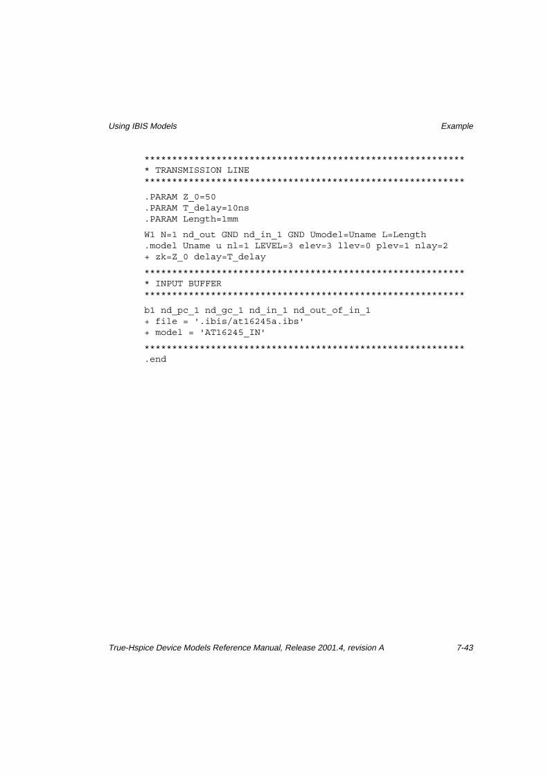
ExampleBelow is a complete example of the netlist that contains an output buffer,transmission line, and input buffer.
A digital signal is supplied to the node nd_in. It is transmitted by the outputbuffer to a network, goes through a transmission line, is received by an inputbuffer, and transformed into digital form and available on node nd_out_of_in_1.IBIS file at16245a.ibs resides in the directory .ibis, which is located in thedirectory from which you run the simulator.
*********************************************************** test for iob: output buffer—transmission line—input buffer**********************************************************
7-44 True-Hspice Device Models Reference Manual, Release 2001.4, revision A
Using the IBIS Buffer ComponentThe Input/Output Buffer Information Specification (IBIS) is being developed bythe IBIS Open Forum, which is affiliated with the Electronic Industries Alliance(EIA).
IBIS specifies a standard form to present information in ASCII format, usingspecial files. This information describes the behavior of various I/O buffers thatsend electrical signals outside the silicon chip, or receive such signals. The typeof information includes:
■ Output I-V curves for output buffers, in LOWand HIGH states.■ V(t) curves, describing the exact form of transitions from LOW to HIGH
states, and from HIGH to LOW states, for a specified load.■ Values for die capacitance.■ Electrical parameters of the packages.
The Avant! True-Hspice models implement buffers as a standard b element. Butto support simulation of IBIS models using .ebd and .pkg, True-Hspice IBISmodels include another component that creates buffers for an integrated circuit.
Understanding the .ibis CommandThe general syntax of the .ibis command for a component is :
keyword_i=value_i Assigns the value_i value, to thekeyword_i keyword. Optional keywordsare in the square brackets.
Using IBIS Models Required Keywords
True-Hspice Device Models Reference Manual, Release 2001.4, revision A 7-45
Required Keywords
file=’file_name’Identifies the IBIS file. file_name must be lower case, and must specify eitherthe absolute path for the file, or the relative path in respect to the directory fromwhich you run simulation.
component=’component_name’Identifies the component for a .ibis command from the IBIS file, specified usingthe file=’...’ keyword. The component_name keyword is case-sensitive, andmust match one of the components from the IBIS file.
subname=’subckt_name’Identifies the subname to which you add the component buffers. The’subckt_name’ must be the name of a sub-circuit that you defined in your Hspicenetlist. The sub-circuit pins must also match the component in the .ibs file.
Note: The component name and file name are defined in the component andfile keywords.
Optional Keywords Using IBIS Models
7-46 True-Hspice Device Models Reference Manual, Release 2001.4, revision A
Optional KeywordsThe following keywords are the same as for the b-element (I/O buffer). For moreinformation, see Specifying Common Keywords on page 7-27.
How .ibis Creates BuffersThe .ibis command adds a buffer to the netlist for every pin, according to thesignal_name and model_name defined in the [Pin] keyword in the .ibs file.
Note: .ibis does not create a buffer if the pin name is a reserved model name,such as POWER, GND, or NC.
buffer_name = ’cname’_’signal_name’
■ cname is defined in the .ibis card in the .sp netlist.■ signal_name is defined in the [Pin] keyword in the .ibs file
Using IBIS Models How .ibis Creates Buffers
True-Hspice Device Models Reference Manual, Release 2001.4, revision A 7-47
The pins, and the elements that connect to these pins in the sub-circuit, aredivided. The node name of the elements are changed from subcircuit’s pins to
’bufn_<pin_number>’
■ <pin_number> is 1 if this pin is the first pin defined in the [Pin] keyword.■ <pin_number> is 2 if this pin is the second pin.
and so on.
The buffers are inserted between the ’bufn_<pin_number>’ node and the pin.
Example
A file named test.ibs contains the following messages:[Component] TEST[Manufacturer] Intel Corporation[Package]| typ min maxR_pkg 50.000mOhm 40.000mOhm 60.000mOhmL_pkg 5.00nH 4.00nH 6.00nHC_pkg 2.00pF 1.00pF 3.00pF
A netlist named test.sp contains the following commands:.ibis comp component=’TEST’+ file=’test.ibs’ subname= ’test’+ [typ=fast]+ [interpol={1}]+ [nowarn]+ .......subckt test vcc1 gnd1 inbuf io50buf.......endsxtest vcc gnd in out test.......
For this example, the .ibis command creates two buffers: ptest_inbuf andptest_io50buf.
Using the Buffer Component Using IBIS Models
7-48 True-Hspice Device Models Reference Manual, Release 2001.4, revision A
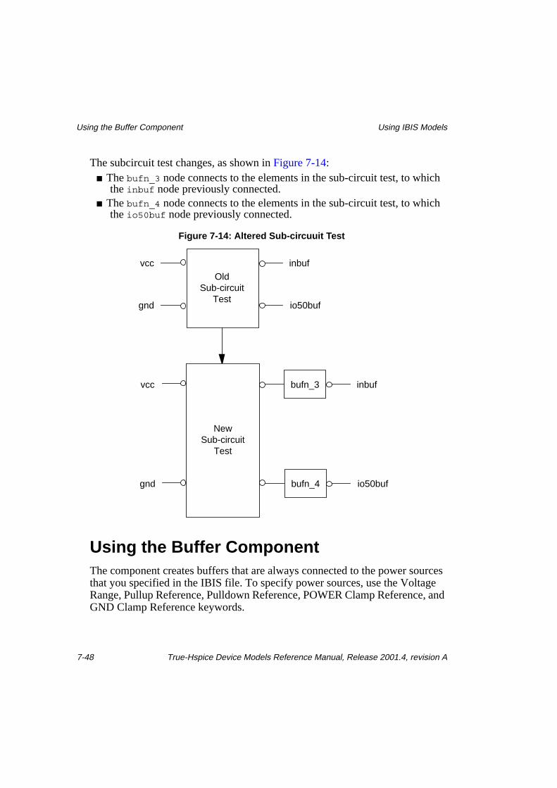
The subcircuit test changes, as shown in Figure 7-14:■ The bufn_3 node connects to the elements in the sub-circuit test, to which
the inbuf node previously connected.■ The bufn_4 node connects to the elements in the sub-circuit test, to which
the io50buf node previously connected.
Figure 7-14: Altered Sub-circuuit Test
Using the Buffer ComponentThe component creates buffers that are always connected to the power sourcesthat you specified in the IBIS file. To specify power sources, use the VoltageRange, Pullup Reference, Pulldown Reference, POWER Clamp Reference, andGND Clamp Reference keywords.
OldSub-circuit
Test
vcc
gnd
inbuf
io50buf
NewSub-circuit
Test
vcc
gnd
bufn_3
bufn_4
inbuf
io50buf
Using IBIS Models Using the Buffer Component
True-Hspice Device Models Reference Manual, Release 2001.4, revision A 7-49
The nodes of buffers expect input and output node names in the followingformat:
where:■ cname is defined in the .ibis card in the the .sp netlist.■ signal_name is defined in the [Pin] keyword in the .ibs file■ <node_name> is different for different types of buffers:
Note: For more information about nodes for different buffers, see Bufferson page 7-6.
The names of the input and output nodes for the buffers are:
INPUT and INPUT_ECL buffers signal name of pin (’in’)’ bufn_<pin_number>’(’outofin’)
Other types of buffers ’bufn_<pin_number>’(’in’)signal name of pin (’out’)
Simulating the Component with pkg and ebd Using IBIS Models
7-50 True-Hspice Device Models Reference Manual, Release 2001.4, revision A
■ <pin_number> is 1 if this pin is the first pin defined in the [Pin] keyword.■ <pin_number> is 2 if this pin is the second pin.
and so on.
Note: If the buffer has an enable terminal, you must create a node namedbuffer_name_en to enable the buffer.
Example
The .ibis command creates an input buffer named ptest_inbuf, and an input-output buffer named ptest_io50buf..subckt test vcc1 gnd1 inbuf io50buf......ven1 ptest_io50buf_en vcc1 0v.endsxtest vcc gnd in out test
rout out gnd 50......
.print v(xtest.ptest_inbuf_pc) $ pc node of ptest_inbuf+ v(xtest.ptest_inbuf_gc) $ gc node of ptest_inbuf+ v(in) $ in node of ptest_inbuf+ v(bufn_3) $ outofin node of ptest_inbuf+ v(xtest.ptest_io50buf_pu) $ pu node of ptest_io50buf+ v(xtest.ptest_io50buf_pd) $ pd node of ptest_io50buf+ v(xtest.ptest_io50buf_outofin) $ outofin node of ptest_io50buf+ v(xtest.ptest_io50buf_pc) $ pc node of ptest_io50buf+ v(xtest.ptest_io50buf_gc) $ gc node of ptest_io50buf+ v(xtest.ptest_io50buf_en) $ enable node of ptest_io50buf+ v(out) $ out node of ptest_io50buf+ v(bufn_4) $ in node of ptest_io50buf
Simulating the Component with pkg and ebdIf you want to simulate the IBIS buffer component with .pkg and .ebd, add thefollowing option:
pkgmap,pkgtyp,ebdmap,ebdtyp
For more information, see the "PKG and EBD Simulation" section in Chapter 3,"Specifying Simulation Input and Controls", in the Star-Hspice Manual.
Using IBIS Models Additional Notes
True-Hspice Device Models Reference Manual, Release 2001.4, revision A 7-51
Additional NotesThis section provides some additional notes about IBIS models, to clarifytechnical issues. Most of this information was developed as a result of customerinteraction.
KeywordsThe fwf_tune, rwf_tune parameters specify transition time for circuitry (eitherpullup or pulldown) that goes from the ON to OFF state as a fraction of time,delta_T, for a transition for the opposite circuitry (either pulldown or pullup)from OFF to ON state. The delta_T value for ramp data transition time isdifferent from the value for single waveform transition time (delta_T depends onparameters ramp_fwf and ramp_rwf). Consequently, the absolute values fortransition time from the ON to OFF state are different for ramp data and singlewaveform data.
Voltage ThresholdsVoltages applied to the input node and enable node are digital signals. Theyshould be either 0 or 1. It is acceptable to specify input voltage as:
V_in nd_in 0 pulse (0 3.3 0 0.5n 0.5n 4n 8n)
However, in-circuit simulation currently detects only two thresholds, 20% and80% of [0,1] swing, i.e., 0.2V and 0.8V. If a buffer is non-inverting and in aLOW state, it will start transition to a HIGH state, if V_in > 0.8V. If the bufferis in HIGH state, it will start the transition to LOW state, if V_in < 0.2V.Specifying input voltage in the range [0, 3.3V] as in the above example does notmake LOW -> HIGH transitions better in any way, but can add uncertainty overtime interval 0.5ns, when the transition actually occurs.
.OPTION D_IBIS Using IBIS Models
7-52 True-Hspice Device Models Reference Manual, Release 2001.4, revision A
.OPTION D_IBISThe d_ibis option specifies the directory where IBIS files are located. Exampleof usage:
.OPTION d_ibis='/home/user/ibis/models'
If several directories are specified, then simulation looks for IBIS files in thelocal directory (the directory from which you run the simulation), then in thedirectories specified through .option d_ibis in the order that .option cards appearin the netlist. At most, four directories can be specified through d_ibis option.Examples of usage:
Sub-modelEach buffer can call one Dynamic_clamp or one Bus_hold.
■ Dynamic_clamp is automatically set to the All mode.■ Bus_hold is automatically set to the Non-driving mode.
Note: If you use more than one Bus_hold, combine them to acquire theaccurate result.
You can define the Off_delay parameter on both the rising edge and the fallingedge. You can use this parameter with both the V_trigger_r and the V_trigger_fparameters.
Driver ScheduleDriver schedule connects the buffers together, to form the more complicatedbuffer behavior. The scheduled buffer should have the same node list as the topbuffer.
Using IBIS Models Driver Schedule
True-Hspice Device Models Reference Manual, Release 2001.4, revision A 7-53
For example, you can use the output buffer to schedule the open_drain buffer.
The delay parameter, such as rise_on_dly, should be consistent with the polarityof the scheduled driver. If the buffer inverts, then the rising edge turns on thepulldown device, and the rise_on_dly parameter means that the pulldown deviceautomatically turns off after the rise_on_dly-rise_off_dly period.
Warning and Error Messages Using IBIS Models
7-54 True-Hspice Device Models Reference Manual, Release 2001.4, revision A
Warning and Error MessagesIf certain conditions are met (or not met), simulation prints warnings or errormessages. Some examples of these messages are described below.
Warnings are issued if the input data is inconsistent. In this case, simulationmodifies data to make consistent and runs the simulation with modified data.Static I/V curves take precedence over V(t) curves and ramp data. If simulationmodifies your data, it is unlikely the results of simulation with a test load willmatch V(t) curves specified in the IBIS file. To achieve high accuracy, input datashould be consistent. Pay close attention to warnings and understand the causes.
Errors are issued if the simulation cannot continue, using the specified data.
Example
An example of a warning:** warning** iob_eles2:205:
text of the warning, line1text of the warning, line2
An example of an error:** error** iob_eles2:205:
text of the error, line1text of the error, line2
Text that follows the comments '** warning**' and '** error**', such as'iob_eles2:205:' identifies the location where the problem occurs. It isintended to help the developer solve the problem.
The following information is intended for users. A list of selected warningsfollows.
1. I/V Curves
PC and GC I-V curves should be equal to zero at zero voltage, I(V=0)=0.If different values are found, a warning is issued. For example, for a PC I/V curve the following warning is issued.
Using IBIS Models Warning and Error Messages
True-Hspice Device Models Reference Manual, Release 2001.4, revision A 7-55
** warning** ffffffff:NNN:POWER_Clamp curve should be zero at originfound value 1.85800E-01I/V curve is not modified
This warning occurs for Power_Clamp and Ground_Clamp I/V curves.Simulation takes these I/V curves as given, but an error is likely to occurif I(V=0) is not zero.
2. I-V curves and rising/falling waveforms (RWF, FWF) should beconsistent.
Simulation verifies consistency for the end points of RWF, FWF. Ifinconsistency is detected, the I/V curves take precedence over V(t) curves,and V(t) curves are modified to make them consistent with I-V curves.** warning** ffffffff:NNN:
Falling WF min estimate and given value differestimate = 3.3540E-01 given = 6.6000E-01
In this example, I/V curves give a value of 3.3540E-01V for minimumvoltage when pullup is OFF (if pullup is available) and pulldown is ON (ifpulldown is available) for load specified for FWF. The minimum voltagevalue of FWF in the IBIS file is 6.6000E-01V. In this case, simulationmodifies the FWF to be consistent with I-V curves.
1. I/V curves and ramp data should be consistent (if ramp is used).
In-circuit simulation verifies consistency for end points of rising edge andfalling edge. The IBIS standard requires that ramp data correspond to 20%to 80% transition of the total voltage change. If inconsistency is detected,the following warning appears:** warning** ffffffff:NNN:Inconsistency between Ramp and PD/PU data is detected.dV_r=1.5900E+00 V_rwf_max=3.3000E+00 V_rwf_min=3.3540E-01transition from 20% to 80% is not satisfiedFILE = gtl-plus.ibsMODEL = io_buf
In this example, voltage changes from 0.3354 V to 3.3 V on the risingedge, as calculated from I/V curves. 60% of this range is 1.78 V. The IBISfile gives 1.59 V. Simulation issues warnings, assumes that the derivativefor the ramp is specified in the IBIS file, and the voltage range ascalculated from I/V curves.
References Using IBIS Models
7-56 True-Hspice Device Models Reference Manual, Release 2001.4, revision A
ReferencesThe official IBIS Open Forum web site is located at:
http://www.eia.org/EIG/IBIS/ibis.htm
This site contains articles introducing IBIS, text of the IBIS standard, examplesof IBIS files, and tools such as the golden parser. The site also links to other websites devoted to IBIS.
Other web and ftp sites that have information about IBIS are: