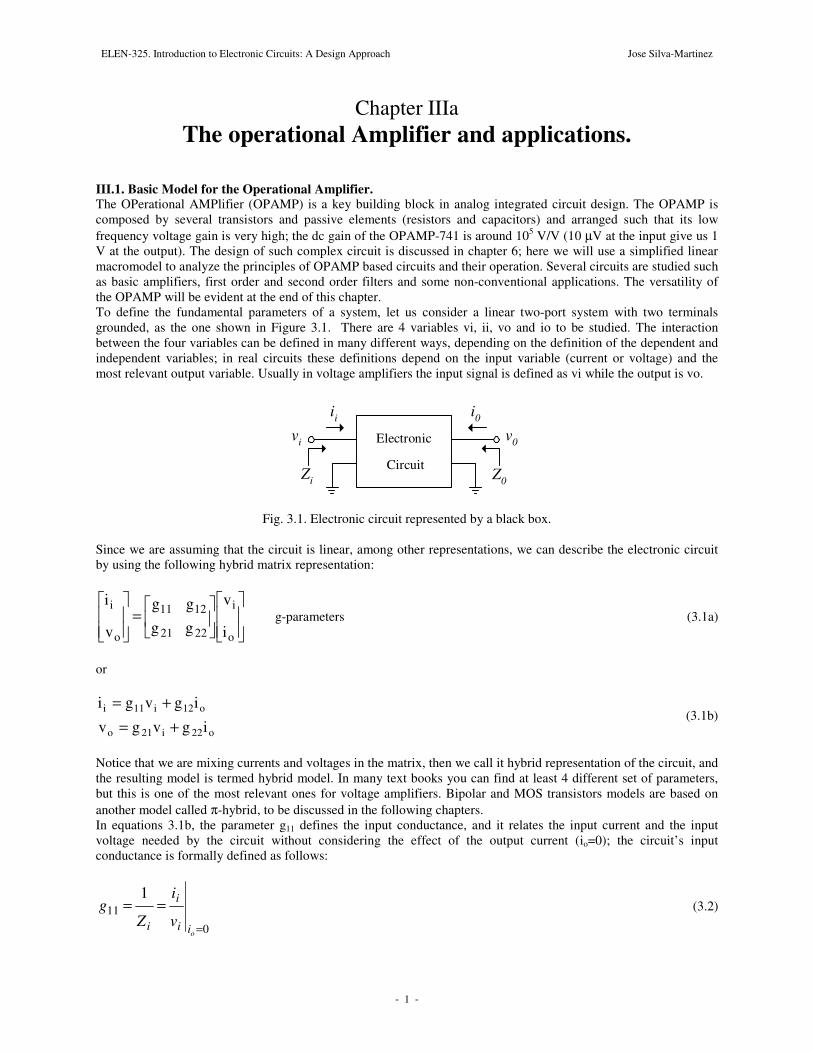
ELEN-325. Introduction to Electronic Circuits: A Design Approach Jose Silva-Martinez - - 1 Chapter IIIa The operational Amplifier and applications. III.1. Basic Model for the Operational Amplifier. The OPerational AMPlifier (OPAMP) is a key building block in analog integrated circuit design. The OPAMP is composed by several transistors and passive elements (resistors and capacitors) and arranged such that its low frequency voltage gain is very high; the dc gain of the OPAMP-741 is around 10 5 V/V (10 μV at the input give us 1 V at the output). The design of such complex circuit is discussed in chapter 6; here we will use a simplified linear macromodel to analyze the principles of OPAMP based circuits and their operation. Several circuits are studied such as basic amplifiers, first order and second order filters and some non-conventional applications. The versatility of the OPAMP will be evident at the end of this chapter. To define the fundamental parameters of a system, let us consider a linear two-port system with two terminals grounded, as the one shown in Figure 3.1. There are 4 variables vi, ii, vo and io to be studied. The interaction between the four variables can be defined in many different ways, depending on the definition of the dependent and independent variables; in real circuits these definitions depend on the input variable (current or voltage) and the most relevant output variable. Usually in voltage amplifiers the input signal is defined as vi while the output is vo. Electronic Circuit v i v 0 i i i 0 Z i Z 0 Fig. 3.1. Electronic circuit represented by a black box. Since we are assuming that the circuit is linear, among other representations, we can describe the electronic circuit by using the following hybrid matrix representation: = o i 22 21 12 11 o i i v g g g g v i g-parameters (3.1a) or o 22 i 21 o o 12 i 11 i i g v g v i g v g i + = + = (3.1b) Notice that we are mixing currents and voltages in the matrix, then we call it hybrid representation of the circuit, and the resulting model is termed hybrid model. In many text books you can find at least 4 different set of parameters, but this is one of the most relevant ones for voltage amplifiers. Bipolar and MOS transistors models are based on another model called π-hybrid, to be discussed in the following chapters. In equations 3.1b, the parameter g 11 defines the input conductance, and it relates the input current and the input voltage needed by the circuit without considering the effect of the output current (i o =0); the circuit’s input conductance is formally defined as follows: 0 11 1 = = = o i i i i v i Z g (3.2)
Transcript
ELEN-325. Introduction to Electronic Circuits: A Design Approach Jose Silva-Martinez
- - 1
Chapter IIIa The operational Amplifier and applications.
III.1. Basic Model for the Operational Amplifier. The OPerational AMPlifier (OPAMP) is a key building block in analog integrated circuit design. The OPAMP is composed by several transistors and passive elements (resistors and capacitors) and arranged such that its low frequency voltage gain is very high; the dc gain of the OPAMP-741 is around 105 V/V (10 µV at the input give us 1 V at the output). The design of such complex circuit is discussed in chapter 6; here we will use a simplified linear macromodel to analyze the principles of OPAMP based circuits and their operation. Several circuits are studied such as basic amplifiers, first order and second order filters and some non-conventional applications. The versatility of the OPAMP will be evident at the end of this chapter. To define the fundamental parameters of a system, let us consider a linear two-port system with two terminals grounded, as the one shown in Figure 3.1. There are 4 variables vi, ii, vo and io to be studied. The interaction between the four variables can be defined in many different ways, depending on the definition of the dependent and independent variables; in real circuits these definitions depend on the input variable (current or voltage) and the most relevant output variable. Usually in voltage amplifiers the input signal is defined as vi while the output is vo.
Electronic
Circuit
vi v0
ii i0
Zi Z0
Fig. 3.1. Electronic circuit represented by a black box.
Since we are assuming that the circuit is linear, among other representations, we can describe the electronic circuit by using the following hybrid matrix representation:
=
o
i
2221
1211
o
i
i
v
gggg
v
i g-parameters (3.1a)
or
o22i21o
o12i11i
igvgv
igvgi
+=+=
(3.1b)
Notice that we are mixing currents and voltages in the matrix, then we call it hybrid representation of the circuit, and the resulting model is termed hybrid model. In many text books you can find at least 4 different set of parameters, but this is one of the most relevant ones for voltage amplifiers. Bipolar and MOS transistors models are based on another model called π-hybrid, to be discussed in the following chapters. In equations 3.1b, the parameter g11 defines the input conductance, and it relates the input current and the input voltage needed by the circuit without considering the effect of the output current (io=0); the circuit’s input conductance is formally defined as follows:
0
111
=
==oii
i
i v
i
Zg (3.2)
ELEN-325. Introduction to Electronic Circuits: A Design Approach Jose Silva-Martinez
- - 2
This parameter is measured by applying an input voltage source and measuring the input current; the output node is left open such that io=0. Since g11 is the ratio of the input current to the input voltage, while the output is leaved open, its units are amps/volts or 1/. The parameter g12 defines the reverse current gain of the topology, and it is defined as
0
12
=
=ivo
i
i
ig (3.3)
This parameter represents the reverse current gain: current generated at the input due to the output current. In the ideal case this parameter is zero since usually the operational amplifiers are unidirectional; e.g. the input signal applied to the system generates an output signal, but the output signals (current or voltage) should not generate any signal at the input. For measuring this parameter it is required to short circuit the input port such that vi=0, then apply a current at the output and measure the current generated at the input port. In practical circuits this parameter is very small and usually it is ignored. The Forward voltage gain is defined as the ratio of the output voltage and input voltage without any load connected at the output.
0
21
=
==oii
oV
v
vAg (3.4)
This is certainly one of the most important parameters of the two-port system; we also refer to AV as the open-loop gain of the OPAMP. It represents the circuit’s voltage gain without any load impedance attached (output current equal zero). Another important parameter is the system’s output impedance, which relates the output voltage and the output current without taking the effects of the input signal. It is defined by
0
022
=
==ivo
o
i
vZg (3.5)
Thus, the two-port system can be represented by the four aforementioned parameters; the resulting macromodel is shown in Figure 3.2. For sake of clarification we are using impedances instead of admittances in this representation. Notice that a current controlled current source (ICCS) is used for the emulation of parameter g12 since it represents the input current (input port) being generated by the output current (output port). A resistor can not represent this parameter since current is flowing in one port but the voltage at the other port controls it. Similar comments apply to the voltage controlled voltage source represented by AV vi (g21vi).
+-
AVvi
Z0
v0
g12i0Zi
vi
i0ii
Fig. 3.2. Linear macromodel of a typical voltage amplifier using hybrid parameters.
Model for the OPAMP. The ideal OPAMP is a device that can be modeled by using the circuit of Fig. 3.2 with AV=∞, g12=0, Zi=∞, and Zo=0. This is of course an unrealistic model, but it is enough for understanding the basic circuits and their operation. We will see that when you connect several circuits in cascade for complex signal
ELEN-325. Introduction to Electronic Circuits: A Design Approach Jose Silva-Martinez
- - 3
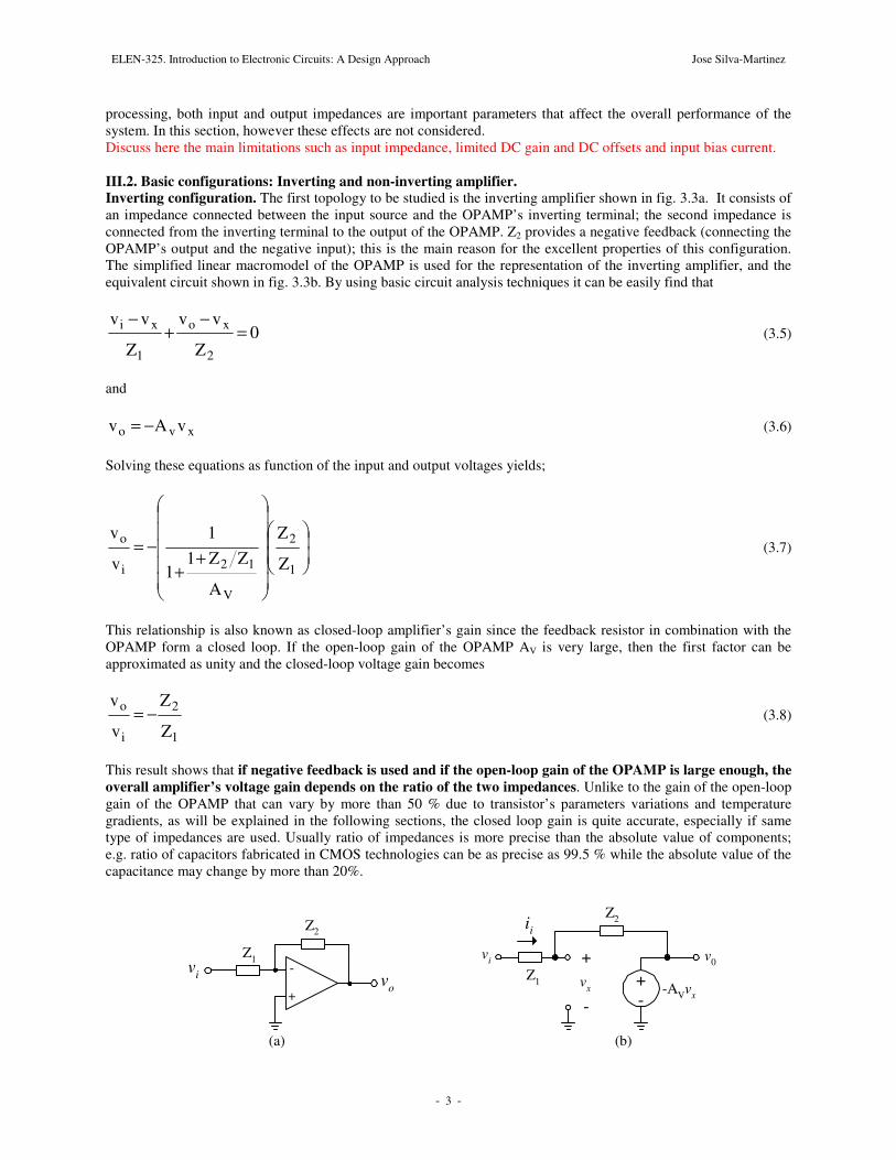
processing, both input and output impedances are important parameters that affect the overall performance of the system. In this section, however these effects are not considered. Discuss here the main limitations such as input impedance, limited DC gain and DC offsets and input bias current. III.2. Basic configurations: Inverting and non-inverting amplifier. Inverting configuration. The first topology to be studied is the inverting amplifier shown in fig. 3.3a. It consists of an impedance connected between the input source and the OPAMP’s inverting terminal; the second impedance is connected from the inverting terminal to the output of the OPAMP. Z2 provides a negative feedback (connecting the OPAMP’s output and the negative input); this is the main reason for the excellent properties of this configuration. The simplified linear macromodel of the OPAMP is used for the representation of the inverting amplifier, and the equivalent circuit shown in fig. 3.3b. By using basic circuit analysis techniques it can be easily find that
0Z
vv
Z
vv
2
xo
1
xi =−
+−
(3.5)
and
xvo vAv −= (3.6) Solving these equations as function of the input and output voltages yields;
++
−=1
2
V
12i
o
Z
Z
A
ZZ11
1
v
v (3.7)
This relationship is also known as closed-loop amplifier’s gain since the feedback resistor in combination with the OPAMP form a closed loop. If the open-loop gain of the OPAMP AV is very large, then the first factor can be approximated as unity and the closed-loop voltage gain becomes
1
2
i
o
Z
Z
v
v−= (3.8)
This result shows that if negative feedback is used and if the open-loop gain of the OPAMP is large enough, the overall amplifier’s voltage gain depends on the ratio of the two impedances. Unlike to the gain of the open-loop gain of the OPAMP that can vary by more than 50 % due to transistor’s parameters variations and temperature gradients, as will be explained in the following sections, the closed loop gain is quite accurate, especially if same type of impedances are used. Usually ratio of impedances is more precise than the absolute value of components; e.g. ratio of capacitors fabricated in CMOS technologies can be as precise as 99.5 % while the absolute value of the capacitance may change by more than 20%.
vi
+
-
vo
Z2
Z1
+-
-AVvx
v0
ii
vi
vx
+
-
Z1
Z2
(a) (b)
ELEN-325. Introduction to Electronic Circuits: A Design Approach Jose Silva-Martinez
- - 4
Fig. 3.3. Inverting amplifier: a) the circuit and b) the linear macromodel assuming that OPAMP input is infinity and output impedance is zero.
Another important observation is that the differential voltage at the OPAMP input vx (see Fig. 3b) is ideally zero. The reasoning behind this observation is as follows: according to 3.8, the output voltage is bounded (not infinity) if Z1 is not zero or Z2 is not infinite, hence vi is also bounded. Under these conditions and according to expression 3.6 the OPAMP input voltage vx is very small if Av is large enough; the larger the OPAMP open loop gain the smaller signal at the input of the OPAMP. Therefore the inputs of the OPAMP can be considered as a virtual short; the voltage difference between the two input terminals (v+ - v-) is very small but they are not physically connected. The virtual short principle is extremely useful in practice; most of the transfer functions can be easily obtained if this property is used. To illustrate its use, let us consider again the circuit of fig. 3.3b. Due to the virtual ground at the input of the OPAMP, vx=0 (virtual short) and the input current ii is determined by vi/Z1. Since the input impedance of the OPAMP is infinite, ii flows throughout Z2, leading to an output voltage given by –iiZ2. As a result, the closed-loop voltage gain becomes equal to -Z2/ Z1, as stated in equation 3.8. If the impedances Z1 and Z2 are replaced by resistors as shown in Fig. 3.4a, we end up with the basic resistive inverting amplifier. The closed-loop gain is then obtained as
vi
+
-
vo
R2
R1
vi
+
-
vo
R2
R1
(a) (b)
Fig. 3.4. Resistive amplifiers: a) inverting configuration and b) non-inverting configuration.
1
2
i
o
R
R
v
v−= (3.9)
Notice that in the case of the inverting configuration, the amplifier’s input impedance is determined by R1; this is a result of the virtual ground present at the inverting terminal of the OPAMP. Hence, if several inverting amplifiers are connected in cascade we have to be aware that the amplifier must be able to drive the input impedance of the next stage. Non-inverting voltage gain configuration. If the input signal is applied at the non-inverting terminal and R1 is grounded, as shown in fig. 3.4b, the non-inverting configuration is obtained. Notice that the feedback is still negative. If R2 is connected to the positive terminal, the circuit becomes unstable and useless for linear applications; this will be evident in the following sections. The closed-loop voltage gain of the non-inverting configuration can be easily obtained if the virtual short principle is used. Due to the high gain of the OPAMP, the voltage difference between the inverting and non-inverting terminals is very small; hence the voltage at the non-inverting terminal of the OPAMP is also vi. The current flowing through R1 and R2 is then given by vi/R1; therefore the output voltage is computed as
( )1
2
i
21ii
i
21i
i
o
RR
1v
RRvvv
Rivvv
+=+
=+
= (3.10)
The voltage gain is therefore greater or equal than 1. An important characteristic of this configuration is that ideally its input impedance is infinity; hence several stages can be easily connected in cascade. A special case of the non-inverting configuration is the buffer configuration shown in figure 3.5. If R1=∞, according to equation 3.10, the voltage gain is unity; in this case the value of R2 is not critical and can even be short-circuited (R2=0). This topology is also known as unity gain amplifier or buffer, and it is very popular for driving small impedances; e.g. speakers, motors, etc.
ELEN-325. Introduction to Electronic Circuits: A Design Approach Jose Silva-Martinez
- - 5
vi
+
-
vo
Rf
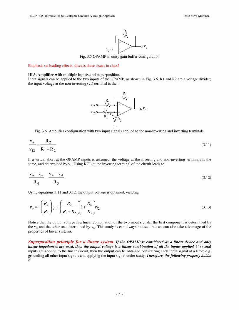
Fig. 3.5 OPAMP in unity gain buffer configuration
Emphasis on loading effects; discuss these issues in class! III.3. Amplifier with multiple inputs and superposition. Input signals can be applied to the two inputs of the OPAMP, as shown in Fig. 3.6. R1 and R2 are a voltage divider; the input voltage at the non-inverting (v+) terminal is then
vi2
+
-
vo
R4
R3vi1
R1 R2
v+
Fig. 3.6. Amplifier configuration with two input signals applied to the non-inverting and inverting terminals.
21
2
2i RR
R
v
v
+=+
(3.11)
If a virtual short at the OPAMP inputs is assumed, the voltage at the inverting and non-inverting terminals is the same, and determined by v+. Using KCL at the inverting terminal of the circuit leads to
3
1i
4
o
R
vv
R
vv −=
− ++ (3.12)
Using equations 3.11 and 3.12, the output voltage is obtained, yielding
23
4
21
21
3
4 1 iio vR
R
RR
Rv
R
Rv
+
++
−= (3.13)
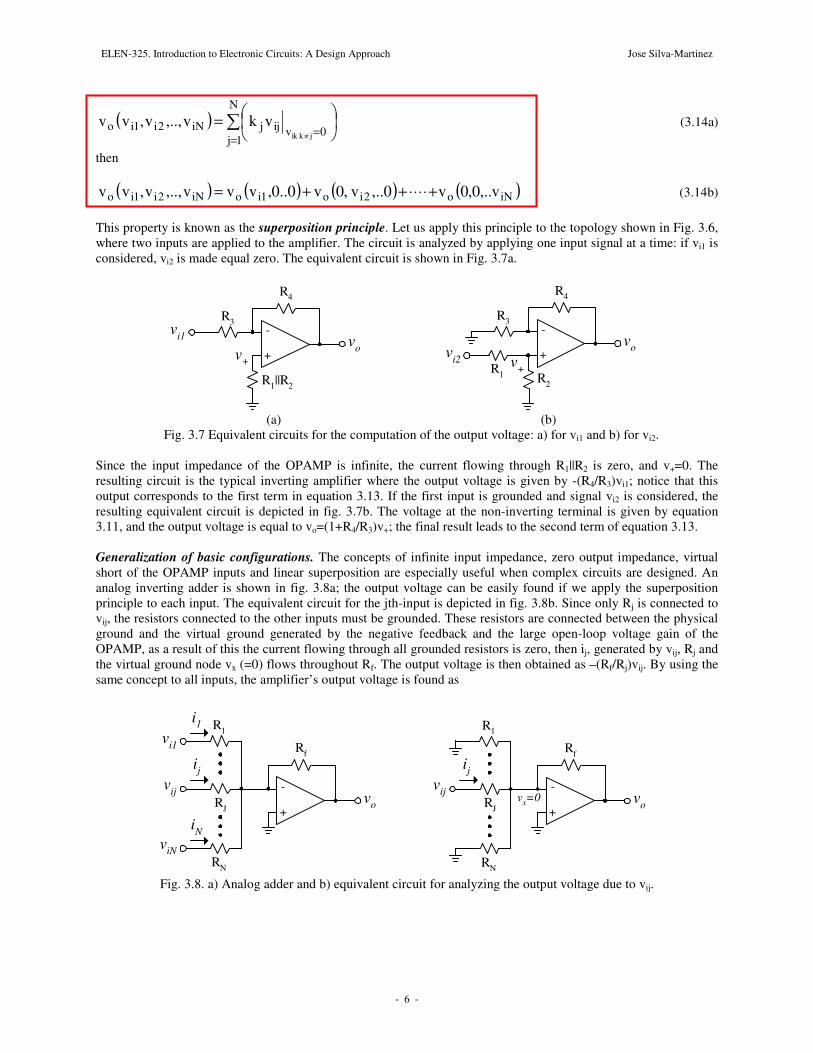
Notice that the output voltage is a linear combination of the two input signals: the first component is determined by the vi1 and the other one determined by vi2. This analysis can always be used, but we can also take advantage of the properties of linear systems. Superposition principle for a linear system. If the OPAMP is considered as a linear device and only linear impedances are used, then the output voltage is a linear combination of all the inputs applied. If several inputs are applied to the linear circuit, then the output can be obtained considering each input signal at a time; e.g. grounding all other input signals and applying the input signal under study. Therefore, the following property holds: if
ELEN-325. Introduction to Electronic Circuits: A Design Approach Jose Silva-Martinez
- - 6
( ) =
=
=≠
N
1j0vjijiN2i1io
jkki
vkv,..,v,vv (3.14a)
then
( ) ( ) ( ) ( )iNo2io1ioiN2i1io v,..0,0v0,..v,0v0..0,vvv,..,v,vv +⋅⋅⋅⋅++= (3.14b) This property is known as the superposition principle. Let us apply this principle to the topology shown in Fig. 3.6, where two inputs are applied to the amplifier. The circuit is analyzed by applying one input signal at a time: if vi1 is considered, vi2 is made equal zero. The equivalent circuit is shown in Fig. 3.7a.
+
-
vo
R4
R3vi1
R1||R2
v+
vi2
+
-
vo
R4
R3
R1 R2
v+
(a) (b)
Fig. 3.7 Equivalent circuits for the computation of the output voltage: a) for vi1 and b) for vi2. Since the input impedance of the OPAMP is infinite, the current flowing through R1||R2 is zero, and v+=0. The resulting circuit is the typical inverting amplifier where the output voltage is given by -(R4/R3)vi1; notice that this output corresponds to the first term in equation 3.13. If the first input is grounded and signal vi2 is considered, the resulting equivalent circuit is depicted in fig. 3.7b. The voltage at the non-inverting terminal is given by equation 3.11, and the output voltage is equal to vo=(1+R4/R3)v+; the final result leads to the second term of equation 3.13. Generalization of basic configurations. The concepts of infinite input impedance, zero output impedance, virtual short of the OPAMP inputs and linear superposition are especially useful when complex circuits are designed. An analog inverting adder is shown in fig. 3.8a; the output voltage can be easily found if we apply the superposition principle to each input. The equivalent circuit for the jth-input is depicted in fig. 3.8b. Since only Rj is connected to vij, the resistors connected to the other inputs must be grounded. These resistors are connected between the physical ground and the virtual ground generated by the negative feedback and the large open-loop voltage gain of the OPAMP, as a result of this the current flowing through all grounded resistors is zero, then ij, generated by vij, Rj and the virtual ground node vx (=0) flows throughout Rf. The output voltage is then obtained as –(Rf/Rj)vij. By using the same concept to all inputs, the amplifier’s output voltage is found as
vij
+
-
vo
Rf
R1vi1
RJ
RN
viN
ij
iN
i1
vij
+
-
vo
Rf
R1
RJ
RN
ij
vx=0
Fig. 3.8. a) Analog adder and b) equivalent circuit for analyzing the output voltage due to vij.
ELEN-325. Introduction to Electronic Circuits: A Design Approach Jose Silva-Martinez
- - 7
=
−=
N
jij
j
fo v
R
Rv
1
(3.15)
An interesting advantage of this circuit is that each one of the input resistors independently controls the voltage gain for each input. This is an important circuit property used for the design of analog-digital converters for instance where the addition of binary weighted signals are required. An analog non-inverting adder is depicted in fig. 3.9a. Similarly to the previous case, the output voltage can be computed by using superposition. Shown in fig. 3.9b is the equivalent circuit for the jth-input signal, and making all other inputs equal zero. The voltage at the non-inverting terminal is the result of the voltage divider determined by the resistors lumped to node v+j as follows:
+
-
vo
Rf
vij
R1
vi1
RJ
RN
viN
RX
Ri
+
-
vo
Rf
vij
R1
RJ
RN
RX
Ri
v+j
a) b)
Fig. 3.9. a) Non-inverting amplifier with multiple inputs and b) equivalent circuit for the jth input.
( ) JXN1J1J21
XN1J1J21
ij
j
RRRRRRR
RRRRRR
v
v
+⋅⋅⋅⋅⋅⋅
⋅⋅⋅⋅⋅⋅=
+−
+−+ (3.16)
Since many components are in parallel, for the analysis of this type of networks it is very often more convenient to use admittances instead of impedances. For this example, the previous equation can also be expressed as
XN1J1J21J
J
ij
j
RRRRRR
1R1
R1
v
v
⋅⋅⋅⋅⋅⋅+
=
+−
+ (3.16b)
The numerator (1/Rj) is identified as the admittance of the element connected between the input signal and v+j. The denominator represents the parallel of all elements attached to v+. The parallel connection of impedances is also equivalent to the reciprocal of the addition of their admittances; then 3.16 can be expressed by the following equivalent expression
( ) =
+
+=
N
1iXi
ij
j
gg
g
v
vJ (3.17)
where gi=1/Ri. Once v+j is obtained, the output voltage generated by vij can be obtained. Since v+j is the voltage at the non-inverting terminal, to find the output voltage for this input is straightforward as voj=(1+Rf/Ri)v+j. Taking into account all the input signals and applying the superposition principle, it can be shown that the overall output voltage is a linear combination of all inputs; the result of this analysis yields,
ELEN-325. Introduction to Electronic Circuits: A Design Approach Jose Silva-Martinez
- - 8
( ) ( )
+
+=
+
+=
+=
=
=
=
=
=+
N
1jijJN
1iXi
i
fN
1jX
N
1ii
ijJ
i
fN
1Jj
i
fo vg
gg
RR
1
gg
vg
RR
1vRR
1v (3.18)
Each input signal has a contribution to the output voltage that depends of all resistors, unlike the case of the inverting topology. The input impedance for each input depends on the array of resistors; for instance the input impedance seen by the jth-input signal is
( )XN1J1J21Jj RRRRRRRZ ⋅⋅⋅⋅⋅⋅+= +− (3.19)
Similar expressions can be obtained for all other input sources. Example: Design a circuit that implements the following equation:
( ) 5v20v10tvo 21 ++= If needed use the supply voltages +/- 15 V. The circuit shown below can be used; this is not the only solution, combinations of inverting and non-inverting circuits might be used as well. The design process consists of finding the resistance values. For that purpose, the following equations must be solved:
+
-vo
R5
v2
R1
R2
R3
R4
v1
+15
++
+=
++
+=
++
+=
321
3
4
5
321
2
4
5
321
1
4
5
gggg
RR
15
gggg
RR
120
gggg
RR
110
Solve this set of equations, and find the numerical values; it is evident that g1=2g3 and that g2=4g3. III.4. Amplifiers with very large gain/attenuation factors. Very large gain amplifiers require large spread of the components. In analog integrated circuits design, it is difficult to control properly such large ratios, and very often they are very demanding of silicon area. Some configurations allow us to reduce this spread. Large gain inverting amplifier using resistors in a T-array. Large voltage gain factors require very large resistors; the array of resistors shown in figure 3.10can be used to “increase” the effective feedback resistor. The circuit’s transfer function can obviously be obtained by using conventional circuit analysis techniques such as KCL. It is however to useful to analyze the circuit based on the following observations:
ELEN-325. Introduction to Electronic Circuits: A Design Approach Jose Silva-Martinez
- - 9
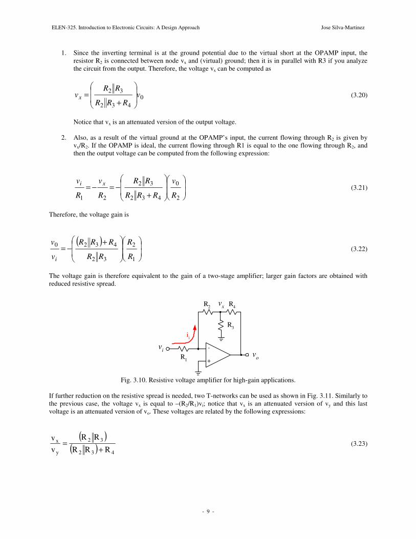
1. Since the inverting terminal is at the ground potential due to the virtual short at the OPAMP input, the resistor R2 is connected between node vx and (virtual) ground; then it is in parallel with R3 if you analyze the circuit from the output. Therefore, the voltage vx can be computed as
0432
32 vRRR
RRvx
+= (3.20)
Notice that vx is an attenuated version of the output voltage.
2. Also, as a result of the virtual ground at the OPAMP’s input, the current flowing through R2 is given by vx/R2. If the OPAMP is ideal, the current flowing through R1 is equal to the one flowing through R2, and then the output voltage can be computed from the following expression:
+−=−=
2
0
432
32
21 R
v
RRR
RR
R
v
R
v xi (3.21)
Therefore, the voltage gain is
( )
+−=
1
2
32
4320
R
R
RR
RRR
v
v
i
(3.22)
The voltage gain is therefore equivalent to the gain of a two-stage amplifier; larger gain factors are obtained with reduced resistive spread.
vi
+
-
R2
voR1
R4
R3
vx
ii
Fig. 3.10. Resistive voltage amplifier for high-gain applications.
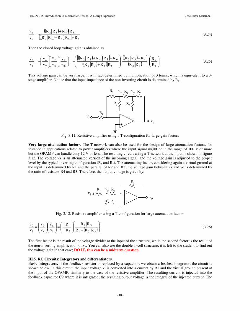
If further reduction on the resistive spread is needed, two T-networks can be used as shown in Fig. 3.11. Similarly to the previous case, the voltage vx is equal to –(R2/R1)vi; notice that vx is an attenuated version of vy and this last voltage is an attenuated version of vo. These voltages are related by the following expressions:
( )( ) 432
32
y
x
RRR
RR
vv
+= (3.23)
ELEN-325. Introduction to Electronic Circuits: A Design Approach Jose Silva-Martinez
- - 10
( )( )( )( )[ ] 65432
5432
0
y
RRRRR
RRRR
v
v
+++
= (3.24)
Then the closed loop voltage gain is obtained as
( )( )[ ]( )( )
( )( )( )
+
+++
−=
−=
1
2
32
432
5432
65432
in
x
x
y
y
o
i
o
RR
RR
RRR
RRRR
RRRRR
vv
v
v
vv
vv
(3.25)
This voltage gain can be very large; it is in fact determined by multiplication of 3 terms, which is equivalent to a 3-stage amplifier. Notice that the input impedance of the non-inverting circuit is determined by R1.
vi
+
-
R2
vo
R1
R4
R3
vx R6
R5
vy
Fig. 3.11. Resistive amplifier using a T-configuration for large gain factors
Very large attenuation factors. The T-network can also be used for the design of large attenuation factors, for instance in applications related to power amplifiers where the input signal might be in the range of 100 V or more but the OPAMP can handle only 12 V or less. The resulting circuit using a T-network at the input is shown in figure 3.12. The voltage vx is an attenuated version of the incoming signal, and the voltage gain is adjusted to the proper level by the typical inverting configuration (R3 and R4). The attenuating factor, considering again a virtual ground at the input, is determined by R1 and the parallel of R2 and R3; the voltage gain between vx and vo is determined by the ratio of resistors R4 and R3. Therefore, the output voltage is given by:
vi
+
-
R1
vo
R4
R3
R2
vx
Fig. 3.12. Resistive amplifier using a T-configuration for large attenuation factors
( )
+
−=
=
321
32
3
4
i
x
x
0
i
0
RRR
RR
RR
vv
vv
vv
(3.26)
The first factor is the result of the voltage divider at the input of the structure, while the second factor is the result of the non-inverting amplification of vx. You can also use the double T-cell structure; it is left to the student to find out the voltage gain in that case; DO IT, this can be a midterm question. III.5. RC Circuits: Integrators and differentiators. Basic integrators. If the feedback resistor is replaced by a capacitor, we obtain a lossless integrator; the circuit is shown below. In this circuit, the input voltage vi is converted into a current by R1 and the virtual ground present at the input of the OPAMP, similarly to the case of the resistive amplifier. The resulting current is injected into the feedback capacitor C2 where it is integrated; the resulting output voltage is the integral of the injected current. The
ELEN-325. Introduction to Electronic Circuits: A Design Approach Jose Silva-Martinez
- - 11
analysis of this circuit can easily be done in the frequency domain where the characteristic impedance of the capacitor is given by 1/(jωC2). The transfer function of the inverting configuration is, as in the previous cases, determined by the ratio of the impedance in feedback and the input impedance, leading to the following result:
vi
+
-
vo
R1
C2
Fig. 3.13. Lossless inverting Integrator
12i
o
CsR1
vv
sH −==)( (3.27)
where s=jω. This circuit has a pole at the origin and a “phantom” zero at ω=∞ (why?). The magnitude response is extremely large at low frequencies, and decreases at higher frequency with a rolloff of –20 dB/decade. The phase response is +90 (-270) degrees and independent of the frequency. Notice that at ω=1/R2C1, the magnitude of the voltage gain is unity. Usually this circuit is not used as a standalone device, but is the key building block for high-order filters and analog-digital converters. The combination of resistors and capacitors lead to the generation of poes and zeros; for example, the circuit implementation of a first order filter is shown in figure 3.14. This circuit is also known as a lossy integrator because while R1 injects charge into C2, the resistor R3 leaks (introduces losses) the charge stored in the capacitor. The gain of this circuit is also determined by the ratio of the equivalent impedance in feedback and the input impedance. In this circuit, the equivalent feedback impedance is composed by the parallel of the impedance of the capacitor (1/jωC2) and R3. The low frequency gain, where the impedance of the capacitor can be ignored, is determined by the ratio of the two resistors; it is evident that the voltage gain is given by –R3/R1. At very high frequencies, the impedance of C2 dominates the feedback and the circuit behaves as the lossless integrator shown in figure 3.19 (gain defined by –1/sR1C2). The overall voltage gain is given by:
vi
+
-
vo
R1
C2
R3
Fig. 3.14. First order lowpass filter
23
1
3
1 CsR
R
R
)s(H+
−= (3.28)
The low-frequency gain is, as expected, determined by the ratio of the resistors. The pole is located at ω=1/R3C2, and for frequencies beyond this frequency the voltage gain decresases with a rolloff of –20 dB/decade. The main differences between this circuit and the passive lowpass filter (voltage divider) are twofold: a) in the active realization (with OPAMP) the low frequency gain can be greater than 1 by adjusting the ratio of the resistors while in the passive filter the gain is always less than 1; b) the OPAMP allows us to connect the circuit to the next
ELEN-325. Introduction to Electronic Circuits: A Design Approach Jose Silva-Martinez
- - 12
stage without affecting the transfer function; this is due to the small output impedance of the OPAMP. A typical transfer function obtained with this circuit is depicted in the following plot;
R3/R1>1
0 dB
11
2
1
3
23
−
=ω
R
R
CRu
1
31010R
Rlog
23
1
CRP =ω
( )logω
Fig. 3.15. Magnitude response for a first order filter.
The unity gain frequency is another important parameter; it can be obtained by taking the magnitude (or square magnitude) of equation 3.28, and equating it to 1. The resulting equation can be solved for the frequency, leading to the following result (find it yourself)
11
2
1
2
12
−
=ω
R
R
CRu (3.29)
For R2>>R1, this frequency is approximately given by ωu=1/R1C1. Notice that for R2<R1 the solution is imaginary, meaning that the unity gain frequency does not exist; in fact you can not find any frequency where the gain is unity for an attenuator (dc gain less trhan 1). For R2<R1, the low frequency gain is less than 1; hence the transfer function does not have any intersection with the 0 dB curve. The general first order transfer function can be implemented by using the topology shown in fig. 3.16. Since the elements are in parallel, it is very convenient o find the voltage gain as the ratio of the equivalent input addmittance and the equivalent feedback addmitance as follows:
vi
+
-
vo
C2
R3
R1
C0
Fig. 3.16. General first order filter
( )
+
+
−=
+
+−=
23
01
1
3
23
01
1
1
CsR
CsR
R
R
sCg
sCgsH (3.30)
With this circuit, you can design the following filters: (a) Lowpass filters if C0 is removed. The pole’s frequency is given by 1/R3C2 (b) Amplifier if C0 and C2 are removed. Gain = -R3/R1 (c) Amplifier if the resistors are removed. Gain = - C0/C2 (not very practical, especially for low frequency
applications)
ELEN-325. Introduction to Electronic Circuits: A Design Approach Jose Silva-Martinez
- - 13
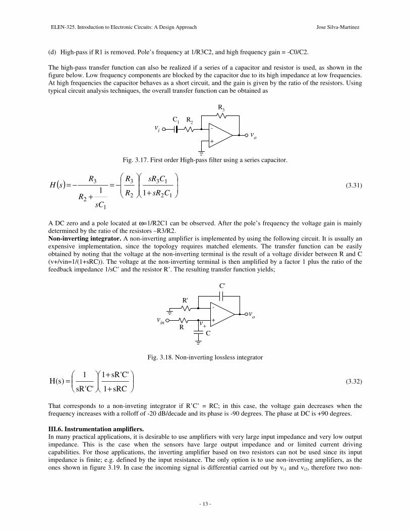
(d) High-pass if R1 is removed. Pole’s frequency at 1/R3C2, and high frequency gain = -C0/C2. The high-pass transfer function can also be realized if a series of a capacitor and resistor is used, as shown in the figure below. Low frequency components are blocked by the capacitor due to its high impedance at low frequencies. At high frequencies the capacitor behaves as a short circuit, and the gain is given by the ratio of the resistors. Using typical circuit analysis techniques, the overall transfer function can be obtained as
vi
+
-
vo
R3
R2C1
Fig. 3.17. First order High-pass filter using a series capacitor.
( )
+
−=
+−=
12
13
2
3
12
3
11 CsR
CsR
R
R
sCR
RsH (3.31)
A DC zero and a pole located at ω=1/R2C1 can be observed. After the pole’s frequency the voltage gain is mainly determined by the ratio of the resistors –R3/R2. Non-inverting integrator. A non-inverting amplifier is implemented by using the following circuit. It is usually an expensive implementation, since the topology requires matched elements. The transfer function can be easily obtained by noting that the voltage at the non-inverting terminal is the result of a voltage divider between R and C (v+/vin=1/(1+sRC)). The voltage at the non-inverting terminal is then amplified by a factor 1 plus the ratio of the feedback impedance 1/sC’ and the resistor R’. The resulting transfer function yields;
vin
+
-
vo
C'
R'
RC
v+
Fig. 3.18. Non-inverting lossless integrator
+
+
=
sRC1
'C'sR1
'C'sR
1)s(H (3.32)
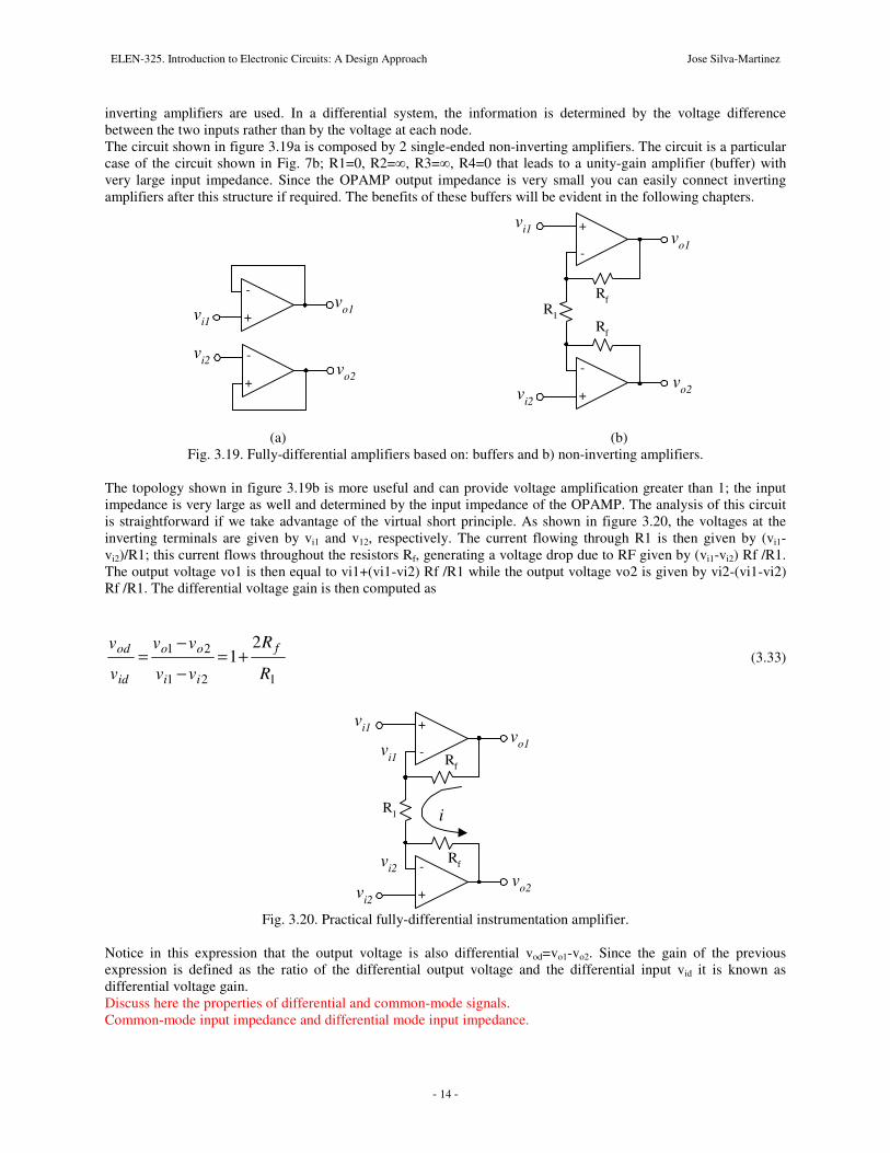
That corresponds to a non-inveting integrator if R’C’ = RC; in this case, the voltage gain decreases when the frequency increases with a rolloff of -20 dB/decade and its phase is -90 degrees. The phase at DC is +90 degrees. III.6. Instrumentation amplifiers. In many practical applications, it is desirable to use amplifiers with very large input impedance and very low output impedance. This is the case when the sensors have large output impedance and or limited current driving capabilities. For those applications, the inverting amplifier based on two resistors can not be used since its input impedance is finite; e.g. defined by the input resistance. The only option is to use non-inverting amplifiers, as the ones shown in figure 3.19. In case the incoming signal is differential carried out by vi1 and vi2, therefore two non-
ELEN-325. Introduction to Electronic Circuits: A Design Approach Jose Silva-Martinez
- - 14
inverting amplifiers are used. In a differential system, the information is determined by the voltage difference between the two inputs rather than by the voltage at each node. The circuit shown in figure 3.19a is composed by 2 single-ended non-inverting amplifiers. The circuit is a particular case of the circuit shown in Fig. 7b; R1=0, R2=, R3=, R4=0 that leads to a unity-gain amplifier (buffer) with very large input impedance. Since the OPAMP output impedance is very small you can easily connect inverting amplifiers after this structure if required. The benefits of these buffers will be evident in the following chapters.
vi1
+
-
vo1
+
-
vo2
vi2
vo1
vi1
RfR1
vi2
+
-
Rf
vo2
+
-
(a) (b) Fig. 3.19. Fully-differential amplifiers based on: buffers and b) non-inverting amplifiers.
The topology shown in figure 3.19b is more useful and can provide voltage amplification greater than 1; the input impedance is very large as well and determined by the input impedance of the OPAMP. The analysis of this circuit is straightforward if we take advantage of the virtual short principle. As shown in figure 3.20, the voltages at the inverting terminals are given by vi1 and v12, respectively. The current flowing through R1 is then given by (vi1-vi2)/R1; this current flows throughout the resistors Rf, generating a voltage drop due to RF given by (vi1-vi2) Rf /R1. The output voltage vo1 is then equal to vi1+(vi1-vi2) Rf /R1 while the output voltage vo2 is given by vi2-(vi1-vi2) Rf /R1. The differential voltage gain is then computed as
Notice in this expression that the output voltage is also differential vod=vo1-vo2. Since the gain of the previous expression is defined as the ratio of the differential output voltage and the differential input vid it is known as differential voltage gain. Discuss here the properties of differential and common-mode signals. Common-mode input impedance and differential mode input impedance.
ELEN-325. Introduction to Electronic Circuits: A Design Approach Jose Silva-Martinez
- - 15
The most popular single-ended instrumentation amplifier is depicted in Fig. 3.21; this topology is very useful for instrumentation applications. There are two inputs, and the important information is in differential format vid=vi1-vi2. A major advantage of fully-differential circuits is that they are little sensitive to noise and signal interferences that affect both inputs; e.g. common-mode signals. The single ended output then should be proportional to vid, and signals that are present in both inputs with same amplitude and same phase are cancelled by the differential nature of the amplifier. Applying the superposition principle to the circuit shown in fig. 3.21, it can be shown that the output voltage is given by a linear combination of vo1 and vo2 as follows:
Using the previous equations 3.33 and 3.34, the output voltage can be obtained as
−
+
−
−
+
+
+= 2
1
21
1
2
3
51
1
22
1
2
3
5
64
6 111 iiiio vR
Rv
R
R
R
Rv
R
Rv
R
R
R
R
RR
Rv (3.35)
After some algebra we get the following result:
( )( )
( )( ) 1
1
2
3
5
1
2
643
5362
1
2
3
5
1
2
643
536 11 iio vR
R
R
R
R
R
RRR
RRRv
R
R
R
R
R
R
RRR
RRRv
+
+
+
+−
+
+
+
+=
. (3.36) If we introduce the conditions R3=R4 and R5=R6, this equation simplifies to the required differential output
( )121
21
3
5 2iio vv
R
RR
R
Rv −
+
= (3.37)
The important properties of this amplifier are: 1. The input impedance is extremely large and determined by the OPAMP. Therefore, it can be easily connected
to a number of sensors regardless the type of sensor’s output impedance. 2. The output voltage is sensitive to differential input voltage vid=vi1-vi2. 3. Common-mode noise present at both terminals is rejected by the differential nature of the topology. The
ability to reject common-mode noise (electromagnetic interference present at both amplifier’s inputs for
ELEN-325. Introduction to Electronic Circuits: A Design Approach Jose Silva-Martinez
- - 16
instance) by an amplifier is measured by the common-mode rejection ratio (CMRR) parameter, to be discussed in next sections.
ELEN-325. Introduction to Electronic Circuits: A Design Approach Jose Silva-Martinez
- - 17
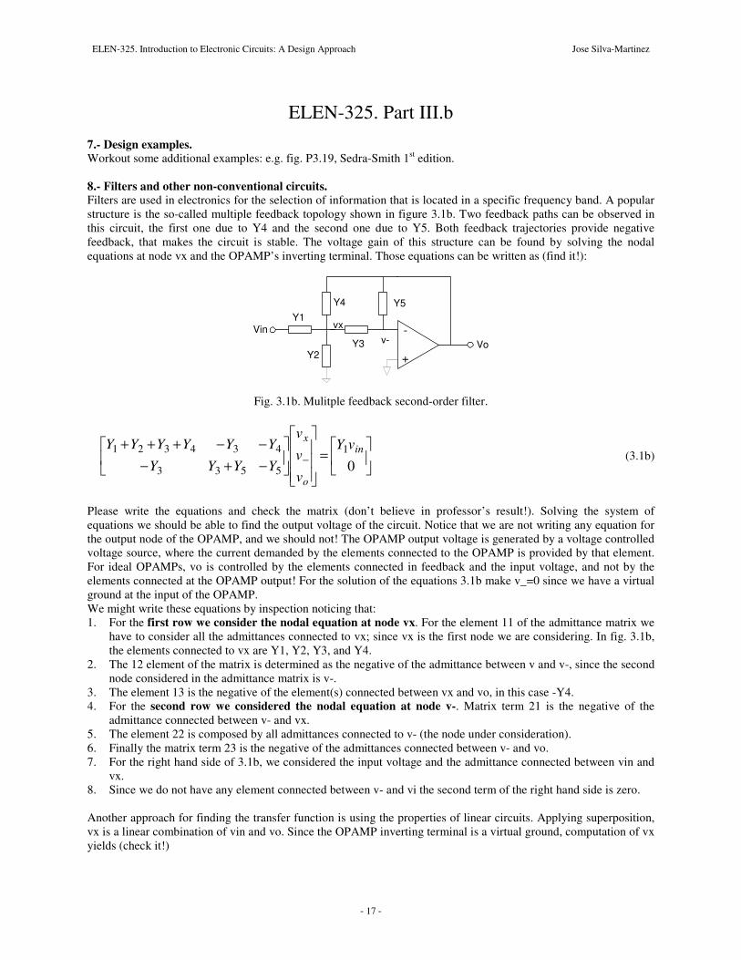
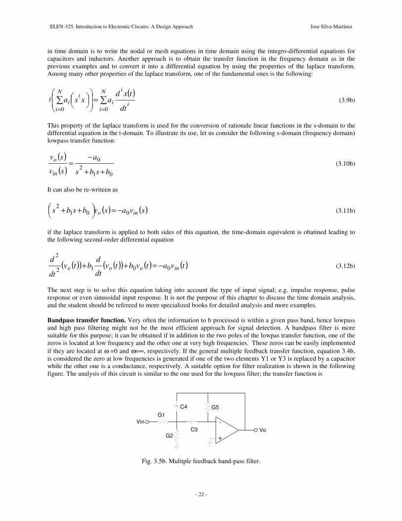
ELEN-325. Part III.b 7.- Design examples. Workout some additional examples: e.g. fig. P3.19, Sedra-Smith 1st edition. 8.- Filters and other non-conventional circuits. Filters are used in electronics for the selection of information that is located in a specific frequency band. A popular structure is the so-called multiple feedback topology shown in figure 3.1b. Two feedback paths can be observed in this circuit, the first one due to Y4 and the second one due to Y5. Both feedback trajectories provide negative feedback, that makes the circuit is stable. The voltage gain of this structure can be found by solving the nodal equations at node vx and the OPAMP’s inverting terminal. Those equations can be written as (find it!):
VinVo
Y1
Y2Y3
Y4 Y5
-
+
vxv-
Fig. 3.1b. Mulitple feedback second-order filter.
=
−+−−−+++
− 01
5533
434321 in
o
x vY
v
v
v
YYYY
YYYYYY (3.1b)
Please write the equations and check the matrix (don’t believe in professor’s result!). Solving the system of equations we should be able to find the output voltage of the circuit. Notice that we are not writing any equation for the output node of the OPAMP, and we should not! The OPAMP output voltage is generated by a voltage controlled voltage source, where the current demanded by the elements connected to the OPAMP is provided by that element. For ideal OPAMPs, vo is controlled by the elements connected in feedback and the input voltage, and not by the elements connected at the OPAMP output! For the solution of the equations 3.1b make v_=0 since we have a virtual ground at the input of the OPAMP. We might write these equations by inspection noticing that: 1. For the first row we consider the nodal equation at node vx. For the element 11 of the admittance matrix we
have to consider all the admittances connected to vx; since vx is the first node we are considering. In fig. 3.1b, the elements connected to vx are Y1, Y2, Y3, and Y4.
2. The 12 element of the matrix is determined as the negative of the admittance between v and v-, since the second node considered in the admittance matrix is v-.
3. The element 13 is the negative of the element(s) connected between vx and vo, in this case -Y4. 4. For the second row we considered the nodal equation at node v-. Matrix term 21 is the negative of the
admittance connected between v- and vx. 5. The element 22 is composed by all admittances connected to v- (the node under consideration). 6. Finally the matrix term 23 is the negative of the admittances connected between v- and vo. 7. For the right hand side of 3.1b, we considered the input voltage and the admittance connected between vin and
vx. 8. Since we do not have any element connected between v- and vi the second term of the right hand side is zero. Another approach for finding the transfer function is using the properties of linear circuits. Applying superposition, vx is a linear combination of vin and vo. Since the OPAMP inverting terminal is a virtual ground, computation of vx yields (check it!)
ELEN-325. Introduction to Electronic Circuits: A Design Approach Jose Silva-Martinez
- - 18
oinx vYYYY
Yv
YYYY
Yv
4321
4
4321
1
++++
+++= (3.2b)
Also, notice that vo is generated by Y5, Y3 and vx as
xo vY
Yv
5
3−= (3.3b)
Solving those equations, the voltage gain can be found as:
( ) 4343215
31
YYYYYYY
YY
v
v)s(H
in
o
++++
−== (3.4b)
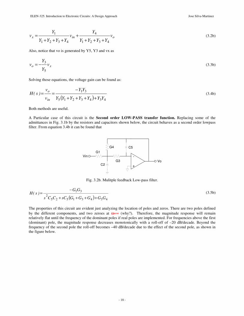
Both methods are useful. A Particular case of this circuit is the Second order LOW-PASS transfer function. Replacing some of the admittances in Fig. 3.1b by the resistors and capacitors shown below, the circuit behaves as a second order lowpass filter. From equation 3.4b it can be found that
VinVo
G1
C2G3
G4 C5
-
+
Fig. 3.2b. Mulitple feedback Low-pass filter.
( ) 434315252
31
GGGGGsCCCs
GG)s(H
++++
−= (3.5b)
The properties of this circuit are evident just analyzing the location of poles and zeros. There are two poles defined by the different components, and two zeroes at ω=∞ (why?). Therefore, the magnitude response will remain relatively flat until the frequency of the dominant poles if real poles are implemented. For frequencies above the first (dominant) pole, the magnitude response decreases monotonically with a roll-off of –20 dB/decade. Beyond the frequency of the second pole the roll-off becomes –40 dB/decade due to the effect of the second pole, as shown in the figure below.
ELEN-325. Introduction to Electronic Circuits: A Design Approach Jose Silva-Martinez
- - 19
ω(log)
20*log10(|H(s)|)
-20 dB/decade
ωP1 ωP2
-40 dB/decade
ωP1=ωP2
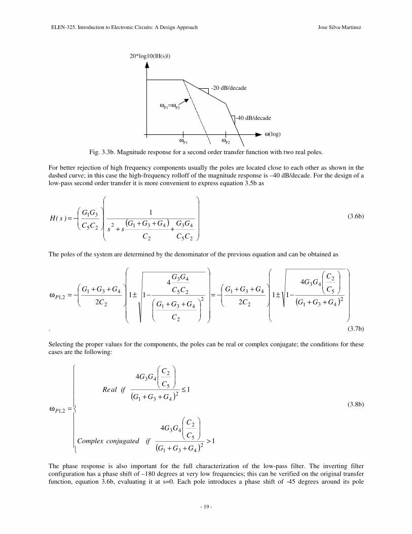
Fig. 3.3b. Magnitude response for a second order transfer function with two real poles.
For better rejection of high frequency components usually the poles are located close to each other as shown in the dashed curve; in this case the high-frequency rolloff of the magnitude response is –40 dB/decade. For the design of a low-pass second order transfer it is more convenient to express equation 3.5b as
( )
+++
+
−=
25
43
2
431225
31 1
CC
GG
C
GGGssCC
GG)s(H (3.6b)
The poles of the system are determined by the denominator of the previous equation and can be obtained as
( )
++
−±
++−=
++−±
++−=ω
2431
5
243
2
4312
2
431
25
43
2
43121
4
112
4
112 GGG
C
CGG
C
GGG
C
GGG
CC
GG
C
GGG,P
. (3.7b) Selecting the proper values for the components, the poles can be real or complex conjugate; the conditions for these cases are the following:
( )
( )
>++
≤++
=ω
1
4
1
4
2431
5
243
2431
5
243
21
GGG
C
CGG
ifconjugatedComplex
GGG
C
CGG
ifalRe
,P (3.8b)
The phase response is also important for the full characterization of the low-pass filter. The inverting filter configuration has a phase shift of –180 degrees at very low frequencies; this can be verified on the original transfer function, equation 3.6b, evaluating it at s=0. Each pole introduces a phase shift of -45 degrees around its pole
ELEN-325. Introduction to Electronic Circuits: A Design Approach Jose Silva-Martinez
- - 20
frequency, as discussed in previous sections. If the poles are far away from each other, the phase response looks like the one depicted by the solid line in the following phase plot.
ω(log)
Phase(H(s))
-45 degrees/dec
ωP1 ωP2
ωP1=ωP2-45 degrees/dec
10ωP10.1ωP1
-180
-235
-270
-315
-360
Fig. 3.4b. Phase response for an inverting second-order transfer function.
If the system have the two poles close to ωP1, then the system’s phase response presents a roll-off of –90 degrees/decade around ωP1, due to phase contribution of two poles, as shown in the dashed plot. The following design example will be discusssed in class: Lowpass filter design: DC GAIN = 20 dB, ωp1=ωp2=100 Krad/sec. The design equations are obtained from the desired filter’s transfer function as follows:
( )( )
ω+ω+
ω−=
ω+ω+
ω−=
21P1P
21P
1P1P
21
s2s
10
ss
10)s(H
Note that the numerator 10ωP1
2 is needed to obtain the desired DC voltage gain. Equation the terms of this equation with the ones of equation 3.6b, the design conditions are obtained R4/R1=10 (105)2=1/(R3R4C2C5) 2(105)=(1/R1+1/R3+1/R4)/ C2
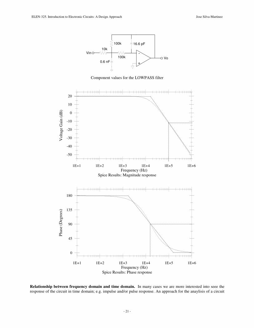
Lets design the filter based on power consumption considerations. To avoid the use of very small resistors, which implies very large currents and more power consumption, lets fix the smaller resistor to R1=10 kΩ and to use R3=R4. Hence: R3=R4 =100 kΩ C2C5 =1/(1010x1010)= 10-20
C2=(1.2x10⁻⁴)/ (2x10⁵)=0.6x10⁻⁹
Then C5 =10-20/0.6x10-9=16.6x10-12. The final design is shown below. The circuit has been simulated in PSPICE, the magnitude and phase response are also shown.
ELEN-325. Introduction to Electronic Circuits: A Design Approach Jose Silva-Martinez
- - 21
VinVo
10k
0.6 nF
100k
-
+
16.6 pF
100k
Component values for the LOWPASS filter
1E+1 1E+2 1E+3 1E+4 1E+5 1E+6Frequency (Hz)
-50
-40
-30
-20
-10
0
10
20
Vol
tage
Gai
n (d
B)
Spice Results: Magnitude response
1E+1 1E+2 1E+3 1E+4 1E+5 1E+6Frequency (Hz)
0
45
90
135
180
Phas
e (D
egre
es)
Spice Results: Phase response
Relationship between frequency domain and time domain. In many cases we are more interested into seee the response of the circuit in time domain; e.g. impulse and/or pulse response. An approach for the anaylisis of a circuit
ELEN-325. Introduction to Electronic Circuits: A Design Approach Jose Silva-Martinez
- - 22
in time domain is to write the nodal or mesh equations in time domain using the integro-differential equations for capacitors and inductors. Another approach is to obtain the transfer function in the frequency domain as in the previous examples and to convert it into a differential equation by using the properties of the laplace transform. Among many other properties of the laplace transform, one of the fundamental ones is the following:
( ) ==
=
N
ii
i
i
N
i
ii
dt
txdaxsa
00 (3.9b)
This property of the laplace transform is used for the conversion of rationale linear functions in the s-domain to the differential equation in the t-domain. To illustrate its use, let us consider the following s-domain (frequency domain) lowpass transfer function:
( )( ) 01
20
bsbs
a
sv
sv
in
o
++
−= (3.10b)
It can also be re-writeen as
( ) ( )svasvbsbs ino 0012 −=
++ (3.11b)
if the laplace transform is applied to both sides of this equation, the time-domain equivalent is obatined leading to the following second-order differential equation
( )( ) ( )( ) ( ) ( )tvatvbtvdt
dbtv
dt
dinooo 0012
2
−=++ (3.12b)
The next step is to solve this equation taking into account the type of input signal; e.g. impulse response, pulse response or even sinusoidal input response. It is not the purpose of this chapter to discuss the time domain analysis, and the student should be refereed to more specialized books for detailed analysis and more examples. Bandpass transfer function. Very often the information to b processed is within a given pass band, hence lowpass and high pass filtering might not be the most efficient approach for signal detection. A bandpass filter is more suitable for this purpose; it can be obtained if in addition to the two poles of the lowpas transfer function, one of the zeros is located at low frequency and the other one at very high frequencies. These zeros can be easily implemented if they are located at ω =0 and ω=∞, respectively. If the general multiple feedback transfer function, equation 3.4b, is considered the zero at low frequencies is generated if one of the two elements Y1 or Y3 is replaced by a capacitor while the other one is a conductance, respectively. A suitable option for filter realization is shown in the following figure. The analysis of this circuit is similar to the one used for the lowpass filter; the transfer function is
VinVo
G1
G2C3
C4 G5
-
+
Fig. 3.5b. Mulitple feedback band-pass filter.
ELEN-325. Introduction to Electronic Circuits: A Design Approach Jose Silva-Martinez
- - 23
( ) ( ) ( ) ( )
++++
−=
++++−=
43
521
43
43524
1
521435432
31
CCGGG
CCCCG
ss
sCG
GGGCCsGCCsCsG
)s(H (3.13b)
The resulting transfer function has two zeros, one at DC and the other one (phantom) at ω=∞. If the poles are at the same frequency, the magnitude and phase responses can be approximated by piece wise linear functions as depicted in the following plots.
ω(log)
20*log10(|H(s)|)
-20 dB/decade
ωP1 ωP2
20 dB/decade
ωP1=ωP2
ω(log)
Phase(H(s))
-45 degrees/dec
ωP1ωP2
ωP1=ωP2
-45 degrees/dec
10ωP10.1ωP1
-90
-135
-180
-225
-270
Fig. 3.6b. Magnitude and phase response of a second order bandpass transfer function. Exercise: Design a Bandpass filter with both poles at 50 MHz and peak gain of 0 dB. Do it! 10.- Partial positive feedback. 10.1 Resistive amplifiers with partial positive feedback. Partial positive feedback can also be used for the implementation of demanding applications. For instance, negative resistors have to be used for the design of voltage controlled oscillators to cancel the effects of resistors lumped to inductors and capacitors (resistive losses). In partial positive feedback circuits, both terminals inverting and non-inverting are embedded in feedback loops; an example is the circuit shown in Fig. 3.7b. The voltage at the positive terminal is a sample of the output voltage vo, and then it can be found that
vi
+
-
R2
vo
R1
R4R3
vx
Fig. 3.7b. Resistive amplifier with negative and positive feedback
ox vRR
Rv
43
3
+= (3.14b)
The output voltage is composed by the contribution of vi (inverting amplifier with a voltage gain =-R2/R1) and vx(non-inverting amplifier given by (1+ R2/R1)vx. Hence, the output voltage can be obtained as:
ELEN-325. Introduction to Electronic Circuits: A Design Approach Jose Silva-Martinez
- - 24
i1
2o
1
2
43
3i
1
2x
1
2o v
R
Rv
R
R1
RR
Rv
R
Rv
R
R1v
−
+
+=
−
+= (3.15b)
The solution of this expression for output voltage yields;
i
43
21
1
3
1
2
o v
RR
RR
R
R1
R
R
v
+
+
−
−= (3.16b)
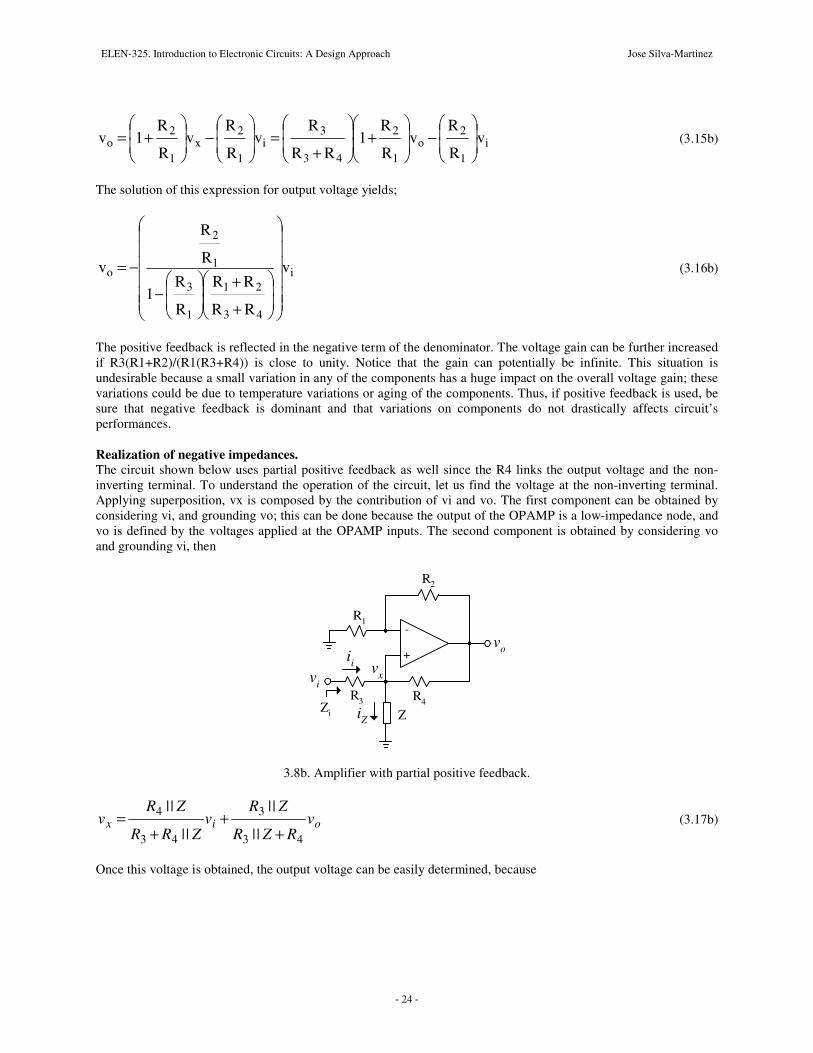
The positive feedback is reflected in the negative term of the denominator. The voltage gain can be further increased if R3(R1+R2)/(R1(R3+R4)) is close to unity. Notice that the gain can potentially be infinite. This situation is undesirable because a small variation in any of the components has a huge impact on the overall voltage gain; these variations could be due to temperature variations or aging of the components. Thus, if positive feedback is used, be sure that negative feedback is dominant and that variations on components do not drastically affects circuit’s performances. Realization of negative impedances. The circuit shown below uses partial positive feedback as well since the R4 links the output voltage and the non-inverting terminal. To understand the operation of the circuit, let us find the voltage at the non-inverting terminal. Applying superposition, vx is composed by the contribution of vi and vo. The first component can be obtained by considering vi, and grounding vo; this can be done because the output of the OPAMP is a low-impedance node, and vo is defined by the voltages applied at the OPAMP inputs. The second component is obtained by considering vo and grounding vi, then
+
-
R2
vo
R1
R4R3
vi
Z
ii
Zi
vx
iZ
3.8b. Amplifier with partial positive feedback.
oix vRZ||R
Z||Rv
Z||RR
Z||Rv
43
3
43
4
++
+= (3.17b)
Once this voltage is obtained, the output voltage can be easily determined, because
ELEN-325. Introduction to Electronic Circuits: A Design Approach Jose Silva-Martinez
- - 25
++
+
+=
+= oixo v
RZ||R
Z||Rv
Z||RR
Z||R
R
Rv
R
Rv
43
3
43
4
1
2
1
2 11 (3.18b)
After some algebra we can find the overall transfer function as
+
+−
+
+
=
43
3
1
2
43
4
1
2
11
1
RZ||R
Z||R
R
R
Z||RR
Z||R
R
R
v
v
i
o (3.19b)
Once again, the positive feedback is reflected in the negative term of the denominator. An important special case is when R1=R2 and R3=R4; the previous equations can be simplified as follows:
( )( ) 333
3 22
R
Z
Z||RR
Z||R
v
v
i
o =−
= (3.20b)
Therefore, the circuit behaves as a non-inverting amplifier. The most interesting properties of this circuit are associated with the input impedance. From 3.17b, it is obtained for the case R1=R2 and R3=R4 that
( ) iioix vR
Zv
R
Z
ZR
Zvv
ZR
Zv
=
+
+=+
+=
3333
21
22 (3.21b)
Therefore the current flowing throughout Z can now be obtained as
3R
v
Z
vi ixZ == (3.22b)
As can be noticed in this result, the current flowing through Z is determined by R3; this current is independent of Z. Therefore, this circuit can be considered as a voltage controlled current source; the current is controlled by the input voltage and the resistors R3=R4, and this current is forced to flow through Z. On the other hand, the impedance at the input port is determined as follows (please work out the following expression).
ZR
R
i
vZ
i
ii
−==
3
23
(3.23b)
For Z<R3 the input impedance is positive, and negative for Z > R3. A useful circuit often used in filter’s design is the negative impedance converter. The circuit, shown in Fig. 3.9b, is a variation of the schematic depicted in Fig. 3.8b. The input voltage is applied to the non-inverting terminal, and the output voltage vo is given by (1+R2/R1)vi. The input current ii is computed as (vi-vo)/Z, leading to the result given in expression 3.24b.
ELEN-325. Introduction to Electronic Circuits: A Design Approach Jose Silva-Martinez
- - 26
vi
+
-
R2
vo
R1
Z
ii ii
Zi Fig. 3.9b. Negative impedance converter.
ZR
RZ
vv
v
i
vZ
oi
i
i
ii
−=
−==
2
1 (3.24b)
Therefore, the equivalent impedance is negative. A negative impedance means that, contrary to the case of a positive impedance, the circuit delivers current when positive signals are applied. The reason for this behavior is that the OPAMP altogether with R1 and R2 amplify the input and the output voltage is greater or equal than vi. Hence positive vi generates vo > vi; since Z is connected between them it generates a current that flows from vo to vi. Think about the following questions: What is the meaning of negative impedance? Difference between positive and negative impedance? 10.2. Sallen & Key Filter. Positive feedback has been use for the design of filters for long time. The filter based on finite gain amplifier uses 5 admittances and an amplifier with finite gain K. Since the amplifier is a non-inverting structure, the feedback produced by Y2 is positive leading to a filter with partial positive feedback. By following the analysis procedure used for the multiple feedback filters, the transfer function can be obtained by written the admittance matrix as follows:
Ky1
y2
y5
y3
y4
vin vo
Fig. 3.10b. Sallen and Key second-Order filter.
=
−−−+−
−−+++
00
100
1
0
433
235321 in
y
x vy
vv
v
Kyyy
yyyyyy
(3.25b)
The first two rows correspond to the nodal equations of nodes vx and vy, respectively. The third row corresponds to the finite amplifier gain given by vo=Kvy. The solution of this system leads to the following filter’s transfer function:
vx Vy
ELEN-325. Introduction to Electronic Circuits: A Design Approach Jose Silva-Martinez
- - 27
( )( ) ( )Kyyyyyyyy
Kyy)s(H
24343521
31
−++++= (3.26b)
Selecting the proper elements lowpass, bandpass and highpass filters can be designed. These especial cases are:
•••• Selecting Y1 and Y3 as conductances, and Y2 and Y4 as capacitive admittances, the resulting transfer function leads to a lowpass transfer function. Even more, Y5 might be removed in this case; the resulting filter is shown in the figure below. Equation 3.27b show the transfer function.
+KVin VoR1 R2
C2
C1`
Fig. 3.11b. Second order Sallen and Key Filter. Notice that tthis filter uses partial positive feedback
( )2121221211
2
2121
11
111
1
CCRRK
CRCRCRss
CCRRK
)s(H
+
−+++
= (3.27b)
Similarly it can be shown that
•••• Y1 and Y4 conductances, and Y3 and Y5 capacitors lead to a bandpass transfer function.
•••• Y2 and Y4 conductances, and Y1 and Y2 capacitors lead to a high-pass transfer function. Find yourself the resulting circuits! You may find one of these topologies in the first midterm. 11. Practical Limitations of the Operational Amplifiers. First at all, we must recognize that practical OPAMP are not even close to the ideal model: infinite input impedance, infinite gain, infinite bandwidth, and unlimited output current capability. Those parameters depends on the topology used (array of transistors , resistors and capacitors, technology used and power consumption); there are tons of different OPAMPs offered by different vendors; eg. Texas Instruments, Fairchild, National Semiconductor, etc. Although the origin of those limitations are not discussed in this course, the effects of on the overall transfer function of these parameters are briefly discussed in this section. A more realistic OPAMP macromodel is depicted in the following schematic.
Zi -(Av)vn
vnvn
vo
voro
Figure 3.12b. Macromodel for the OPAMP.
Some values for comercially available OPAMPs are: Zi = 1MΩ, r0=10Ω, and Av=105. These parameters introduce errors in the transfer function. Usually it is cumbersome to obtain the final results, and it is difficult to evaluate
ELEN-325. Introduction to Electronic Circuits: A Design Approach Jose Silva-Martinez
- - 28
system degradation especially for complex circuits. Here we obtain some results for a single inverting amplifier but most of the conclusins for this circuit are also valid for complex circuits. Let us consider the circuit shown in Figure 3.13b; we are considering the finite input impedance of the OPAMP Zi and the input impedance of the stage driven by the OPAMP. Using the macrodel of Fig. 3.12b with r0=0, the equivalent circuit can be obtained as depicted in Figure 3.13 (b). The transfer function can be obtained if the nodal equation at node v- is written; notice that nodal equation at the OPAMP output can not be written becausevo is controlled by the voltage dependent voltage source (vo=Av(v+-v-). The current demanded by ZF and ZL is provided by the ideal voltage source. Solving the fundamental equation (i1=ii+i0) the circuit’s transfer funcion yields,
vivo
Z1
Zi
ZF
ZL
+
-
vivo
Z1
Zi
ZF
-vo/AV
i1 ii
i0
ZLAV(v+-v- )
v-
v++
-
Fig. 3.13b. a) Inverting amplifier with OPAMP input impedance Zi and load impedance ZL, and b) equivalent circuit
with r0=0.
( ) ( )
++
−=
v
iFFi
F
A
ZZZZZ
Z)s(H
11
1 (3.29b)
The effect of the finite DC gain and finite input impedance on the inverting amplifier can be better appreciated if the error function is considered; from equation 3.29b it follows that
( )ξ−
−≅
ξ+
−= 1
1
1
i
F
i
F
Z
Z
Z
Z)s(H (3.30b)
where the error function is defined as
( ) ( )
=
+=ξ
i
F
vv
iFF
ZZ
Z
AA
ZZZZ)s(
1
1 1 (3.31b)
If the OPAMP DC gain is limited, the assumption of virtual ground is not longer valid since any output voltage variation generates a finite variation on the differential input signal given by vo/Av. The smaller the OPAMP gain the larger the voltage variations at the OPAMP input are; hence the error should be inversely proportional to Av. The voltage variations on the non-inverting terminal lead to current errors: firstly the input current is given by (vi-v-)/Z1 hence an error proportional to Z1 (ierror1= -v-/Z1) is introduced; Secondly, the OPAMP input impedance takes part of the current generated by Z1, leading to a second current error given by ierror2= v-/ZI. These current errors are converted into voltage errors by the feedback resistor RF, and are evident in equation 3.31b. Notice that even if the OPAMP input impedance is infinite, a gain error due proportional to the ideal gain ZF/Z1 is present. For a given OPAMP open-loop gain Av, the larger the closed-loop amplifier’s gain the larger the error is. The error that can be tolerated depends on the applications; notice that to kept the error below 1 % for instance it is required to satisfy
ELEN-325. Introduction to Electronic Circuits: A Design Approach Jose Silva-Martinez
- - 29
0101
1
.ZZ
Z
A)s(
i
F
v
<
=ξ (3.32b)
For instance if Zi=1 MΩ, and voltage gain of –10, the voltage gain needed depends on the absolute values of the resistors used, as shown in table below
ZF/Zi AV 100/10 > 1000 10k/1k > 1001
1M/100k >1100 10M/1M >2000
Notice that the errors are important when the input impedance Z1 is comparable with the OPAMP input impedance Zi. Another important limiting factor is of course the desired amplifier gain ZF/Zi. Notice that 3.31b can also be re-written as
+
=ξ
i
iF
v Z
ZZ
Z
Z
A)s( 1
1
1 (3.33b)
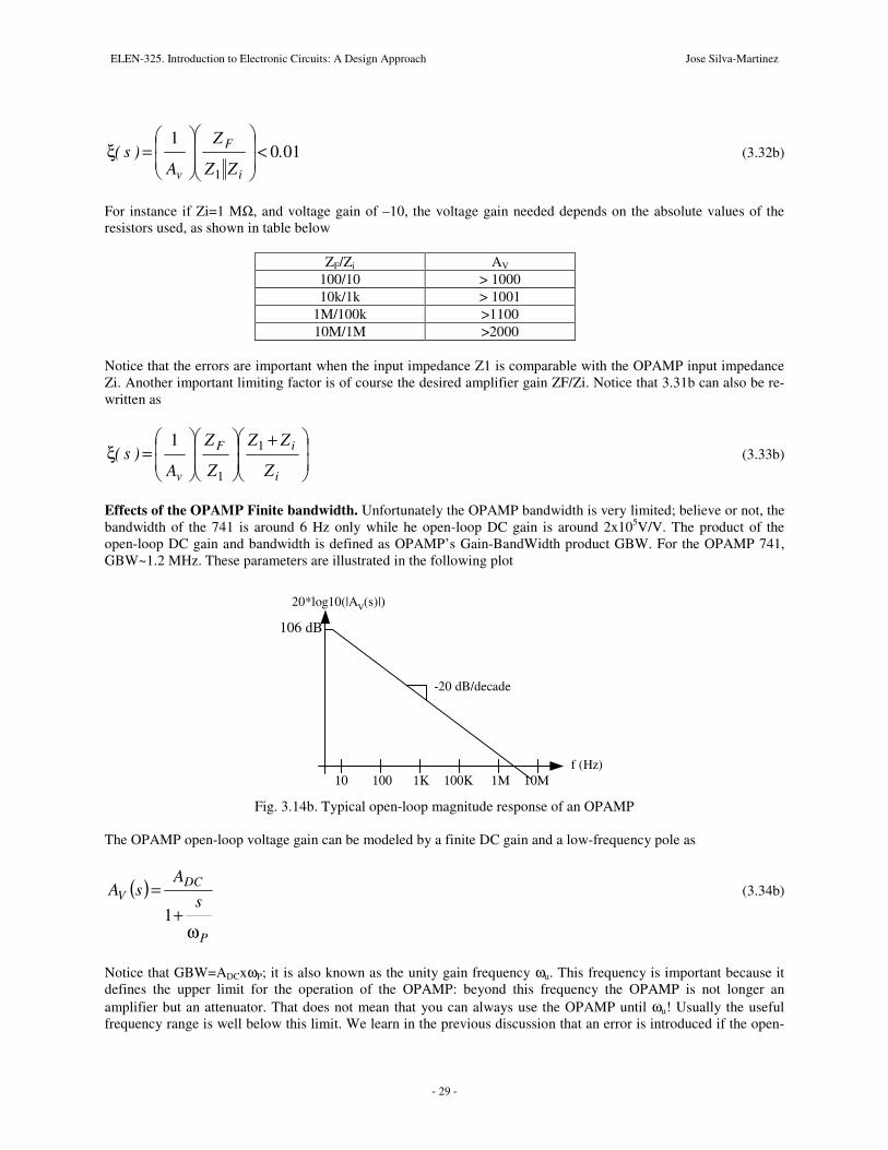
Effects of the OPAMP Finite bandwidth. Unfortunately the OPAMP bandwidth is very limited; believe or not, the bandwidth of the 741 is around 6 Hz only while he open-loop DC gain is around 2x10⁵V/V. The product of the open-loop DC gain and bandwidth is defined as OPAMP’s Gain-BandWidth product GBW. For the OPAMP 741, GBW~1.2 MHz. These parameters are illustrated in the following plot
f (Hz)
20*log10(|AV(s)|)
-20 dB/decade
10 100 1Κ 100Κ 1Μ 10Μ
106 dB
Fig. 3.14b. Typical open-loop magnitude response of an OPAMP
The OPAMP open-loop voltage gain can be modeled by a finite DC gain and a low-frequency pole as
( )
P
DCV s
AsA
ω+
=1
(3.34b)
Notice that GBW=ADCxωP; it is also known as the unity gain frequency ωu. This frequency is important because it defines the upper limit for the operation of the OPAMP: beyond this frequency the OPAMP is not longer an amplifier but an attenuator. That does not mean that you can always use the OPAMP until ωu! Usually the useful frequency range is well below this limit. We learn in the previous discussion that an error is introduced if the open-
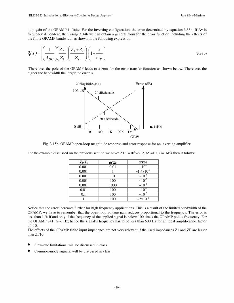
ELEN-325. Introduction to Electronic Circuits: A Design Approach Jose Silva-Martinez
- - 30
loop gain of the OPAMP is finite. For the inverting configuration, the error determined by equation 3.33b. If Av is frequency dependent, then using 3.34b we can obtain a general form for the error function including the effects of the finite OPAMP bandwidth as shown in the following expression:
ω+
+
=ξ
Pi
iF
DC
s
Z
ZZ
Z
Z
A)s( 1
1 1
1
(3.33b)
Therefore, the pole of the OPAMP leads to a zero for the error transfer function as shown below. Therefore, the higher the bandwidth the larger the error is.
f (Hz)
20*log10(|AV(s)|)
-20 dB/decade
10 100 1Κ 100Κ 1Μ
106 dB
GBW
0 dB
20 dB/decade
Error (dB)
Fig. 3.15b. OPAMP open-loop magnitude response and error response for an inverting amplifier.
For the example discussed on the previous section we have: ADC=105v/v, ZF/Z1=10, Zi=1MΩ then it folows:
Notice that the error increases further for high frequency applications. This is a result of the limited bandwidth of the OPAMP; we have to remember that the open-loop voltage gain reduces proportional to the frequency. The error is less than 1 % if and only if the frequency of the applied signal is below 100 times the OPAMP pole’s frequency. For the OPAMP 741; fP=6 Hz; hence the signal’s frequency has to be less than 600 Hz for an ideal amplification factor of -10. The effects of the OPAMP finite input impedance are not very relevant if the used impedances Z1 and ZF are lesser than Zi/10.
•••• Slew-rate limitations: will be discussed in class.
•••• Common-mode signals: will be discussed in class.