71
Class Notes, 31415 RF-Communication Circuits Chapter VI OSCILLATORS Jens Vidkjær NB234

Class Notes, 31415 RF-Communication Circuits
Chapter VI
OSCILLATORS
Jens Vidkjær
NB234

ii

Contents
VI Oscillators . . . . . . . . . . . . . . . . . . . . . . . . . . . . . . . . . . . . . . . . . . . . . . . . . . . 1VI-1 Oscillator Basics . . . . . . . . . . . . . . . . . . . . . . . . . . . . . . . . . . . . . . . 2
Prototype Feedback Oscillators . . . . . . . . . . . . . . . . . . . . . . . . . . . 3Negative Conductance Criteria . . . . . . . . . . . . . . . . . . . . . . . . . . . 7Frequency Stability . . . . . . . . . . . . . . . . . . . . . . . . . . . . . . . . . . . 8Amplitude Stability . . . . . . . . . . . . . . . . . . . . . . . . . . . . . . . . . . . 10Oscillator Noise . . . . . . . . . . . . . . . . . . . . . . . . . . . . . . . . . . . . . . 11
VI-2 Oscillator Circuits . . . . . . . . . . . . . . . . . . . . . . . . . . . . . . . . . . . . . . 15LC Oscillators . . . . . . . . . . . . . . . . . . . . . . . . . . . . . . . . . . . . . . . 15Simplified Analysis of Colpitts Family of Oscillators . . . . . . . . . . . . 18
Case 1 in load resistor placement . . . . . . . . . . . . . . . . . . . 19Case 2 in load resistor placement . . . . . . . . . . . . . . . . . . . 21Case 3 in load resistor placement . . . . . . . . . . . . . . . . . . . 22Arbitrary resistor placements . . . . . . . . . . . . . . . . . . . . . . . 24Example VI-2-1 ( Seiler type LC oscillator ) . . . . . . . . . . . 25Example VI-2-2 ( Pierce type LC oscillator ) . . . . . . . . . . . 29
VI-3 Crystal Oscillators . . . . . . . . . . . . . . . . . . . . . . . . . . . . . . . . . . . . . . 35Crystal Equivalent Circuits . . . . . . . . . . . . . . . . . . . . . . . . . . . . . 35Loading and Driving Crystals . . . . . . . . . . . . . . . . . . . . . . . . . . . . 41Crystal Oscillator Circuits . . . . . . . . . . . . . . . . . . . . . . . . . . . . . . . 44
Example VI-3-1 ( IC-connected crystal oscillators ) . . . . . . . 46APPENDIX VI-A Oscillator Amplitude Stability . . . . . . . . . . . . . . . . . . . . 49
Example VI-A-1 ( amplitude stability ) . . . . . . . . . . . . . . . 54Example VI-A-2 ( amplitude stability with current bias ) . . . 57
Problems . . . . . . . . . . . . . . . . . . . . . . . . . . . . . . . . . . . . . . . . . . . . . . . . 61References and Further Reading . . . . . . . . . . . . . . . . . . . . . . . . . . . . . . . . 65
Index . . . . . . . . . . . . . . . . . . . . . . . . . . . . . . . . . . . . . . . . . . . . . . . . . . . . . . . . . 67
J.Vidkjær iii

J.Vidkjæriv

1
VI Oscillators
Most communication system and measurement equipment include oscillators and theyare often key components that directly influence system specifications and tolerances. There-fore, oscillator design objectives commonly encompass one or more of the following questionin addition to the basic requirement of producing periodic waveshapes.
- Frequency sensitivity and drift in short and long terms
- Waveshapes and Harmonic distortion
- Noise
- Frequency control and adjustment range
To address the fundamental properties in an instructive manner, we shall startconsidering some prototype oscillator circuits, where the different aspects of oscillatorperformance may be separately considered. The prototype oscillators are simple because theyinclude transformer-coupled feed-back paths. In practical circuits transformers are oftenavoided and the feed-back paths may be more difficult to identify.
It is not possible here to cover more than a few of the oscillator circuits that are inpractical use. Below we consider and exemplify one very common family of oscillator circuitsin some depth. Other oscillator types may be treated equivalently using the approaches thatare demonstrated here, so the reader should be able to conduct investigations of other circuitson his own as necessary.
One topic is given more attention here than in most other introductory texts, namelythe mechanisms of amplitude control. This is a topic that must be addressed in every oscillatordesign, but since it is strongly nonlinear, it is often considered as a problem to be dealt withexperimentally. Below, however, we benefit from the presentation of nonlinear amplifiers inthe foregoing chapter and include amplitude control in the design examples. Also the moreadvanced problem of amplitude stability is considered but, due to the lengthy calculations, inan appendix.
J.Vidkjær

2
VI-1 Oscillator Basics
Fig.1 Basic oscillator components and the corresponding signal flow-graph.
Oscillator circuits for sinusoidal oscillations include functions that may be illustratedby the block-diagram of Fig.1. There is a level dependent - i.e. a nonlinear - amplificationA(Vin), which stabilizes the amplitude of oscillation, and a frequency selective positivefeedback circuit b(ω), which determines the frequency of oscillations. Besides the voltage fromthe feedback loop around the amplifier, an additional input voltage Vn that represents eitheramplifier noise or a fast decaying signal is inserted. It is required to start oscillations,especially in analytical models or simulations. The voltage transfer function, which isillustrated by the flow-graph, implies
Self sustained oscillations are possible at a frequency ω0 and an amplifier input Vin0, where
(1)
the transfer function above becomes singular. This properties, which implies a loop gain equalto one, is known as Barkhausen’s condition,
The criterion must be applied in a strictly complex sense so the equation constrains real parts
(2)
or phasor lengths if, simultaneously, the imaginary parts or the phasor angles are forced tozero. To ensure start of oscillation and subsequently amplitude stabilization, the loop gainmust start being greater than one with no amplitude and then decrease monotonously untilBarkhausen’s criterion is met at the desired amplitude. A characteristic like the one in Fig.2has this property.
Fig.2 Nonlinear amplifier characteristic for oscillator amplitude stabilization.
J.Vidkjær

3VI-1 Oscillator Basics
Separation into a nonlinear amplifier circuit and a frequency selective feedbacknetwork may not be as distinct in practice as suggested by the initial presentation above.Designing oscillators it is important, however, to identify the two functions and assure thatthey are working properly under influence of each other including the ability to start oscilla-ting at the required frequency. More detailed accounts on such basic questions may be foundin ref´s [1],[2].
Prototype Feedback Oscillators
We shall start our discussion of oscillators by considering simple circuits where the
Fig.3 Oscillator circuit with class AB or C amplification ( class depends on circuitparameters ). The transistor equivalent in (c) assumes no saturation and relatesfundamental frequency components.
frequency is determined by a parallel resonance circuit, sometimes referred to as the tank-circuit. The tuning inductance is primary winding in a transformer, where feedback is takenfrom the secondary winding. Candidates for an amplifier are the parallel-tuned large-signalamplifiers with current or resistor biasing or the differential amplifier. They have bothdecreasing gain with increasing input drive voltage as it was discussed in section 5-3. Anoscillator with a single transistor is shown in Fig.3(a), and although a circuit with a separatefeed-back winding may be impractical in practice, it is easily understood and it will be avehicle in the present introductory discussion. Fig.3(c) shows the large signal equivalent circuitfor the transistor. Numerical methods were employed in Chap.5 - Eqs.(5-101) through (5-107)-to find the large-signal transconductance Gm, which is a function of the drive level Vb1. Itwas assumed that the transistor operates free of saturation, and that the Q-factor is highenough to ensure a sinusoidal base-emitter voltage around the mean voltage Vb0,
Investigation of Barkhausen’s condition in an oscillator circuit may be done as shown
(3)
by the equivalent circuit in Fig.4, where we - hypothetically - have opened the loop inside the
J.Vidkjær

4 Oscillators
transistor. Connecting input and output ports in this circuit establishes the oscillator with Vb1
Fig.4 Equivalent circuit for calculating open loop gain. Rlp represents possible losses ininductor L. Oscillations are established by connecting the two ports as indicated bythe dashed line.
= V´b1, a condition that also must apply to the open-loop equivalent circuit, where thecondition now reads,
To get correct sign in the condition, the transformer winding is turned to cancel the sense of
(4)
Gm in common emitter configuration. The total parallel resistance of Zp is combined from theexternal load, RLP, a possible inductor loss, Rlp, and the transistor input resistance Rπ seenthrough the transformer, which has winding ratio N. We get
where QL is the Q-factor of the inductor at the resonance frequency ω0. The impedance of the
(5)
parallel tuned circuit is expressed
Frequency dependency is here kept in the function β(ω), which was introduced in Chap.II,
(6)
Eq.II(6). The function, which becomes zero at the resonance frequency, should not beconfused with the transistor current gain βf. The Q-factor Ql is the loaded Q, which includesall resistances in the resonance circuit. The resonance frequency expression may be consideredas the imaginary part of Barkhausen’s requirement since at resonance Zp gets no imaginarypart. The condition becomes
J.Vidkjær

5VI-1 Oscillator Basics
Incorporating the relationship between the effective fundamental frequency transconductance
(7)
and input resistance of the transistor,
we get from the real-part requirement
(8)
The last, approximate, expression assumes that the transformer winding ratio over the
(9)
transistor current gain βf is small. This will be the common situation with N less than one andcurrent gain significantly greater than one. Observe that the effect of the assumption is todisregard the loading of the resonance circuit by the transistor input resistance.
Had we insisted in a strict identification of the two basic oscillator blocks from Fig.1in the present circuit, it would be a natural choice to let the center frequency gain representthe level dependent amplifier, and let the feedback through the secondary winding be thefrequency selective block, i.e.
We may think in terms of this separation when basic stability and noise properties of oscilla-
(10)
tors are discussed in subsequent paragraphs.
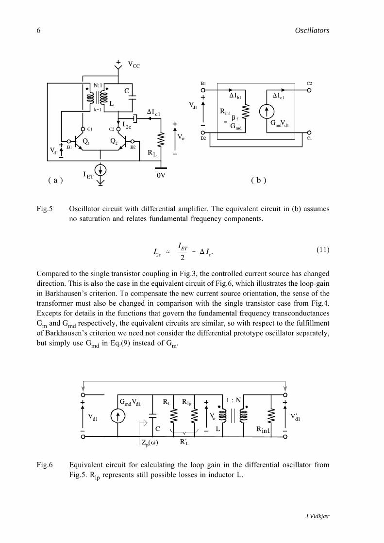
Instead of employing a limiting amplifier with one transistor in the prototypeoscillator, the differential stage could also be used. An example is shown in Figure 5-57.Inser-ted in (b) is the large signal equivalent circuit of a differential pair from Chap.5, Fig.5-54,now with terminal grounded according to the diagram of the complete oscillator. The totalcollector current in transistor Q2 is includes a DC component of approximately half the tailcurrent IET and the differential current ΔIc, where, cf. Eqs.(5-140) and (5-141),
J.Vidkjær
6 Oscillators
Compared to the single transistor coupling in Fig.3, the controlled current source has changed
Fig.5 Oscillator circuit with differential amplifier. The equivalent circuit in (b) assumesno saturation and relates fundamental frequency components.
(11)
direction. This is also the case in the equivalent circuit of Fig.6, which illustrates the loop-gainin Barkhausen’s criterion. To compensate the new current source orientation, the sense of thetransformer must also be changed in comparison with the single transistor case from Fig.4.Excepts for details in the functions that govern the fundamental frequency transconductancesGm and Gmd respectively, the equivalent circuits are similar, so with respect to the fulfillmentof Barkhausen’s criterion we need not consider the differential prototype oscillator separately,but simply use Gmd in Eq.(9) instead of Gm.
Fig.6 Equivalent circuit for calculating the loop gain in the differential oscillator fromFig.5. Rlp represents still possible losses in inductor L.
J.Vidkjær

7VI-1 Oscillator Basics
Negative Conductance Criteria
Fig.7 Redrawing of Fig.4 without Rlp and Rπ1 (a), illustrating the negative conductancepoint of view in oscillator design. Negative conductance is found by the setup in (b).
Instead of Barkhausen’s criterion, the conditions for oscillation may sometimes beformulated from a negative conductance or negative resistance point of view1. In an un-damped resonance circuit, oscillation will continue forever at the resonance frequency oncethey have been started. If power is taken from the circuit by parallel loading through apassive, i.e. positive, conductance, continued oscillation requires continuous supply of power.To maintain the conditions for an undamped resonator, the model of the circuitry that deliverspower must contain a conductance in parallel to the load of same size but with negative sign.We may illustrate the method by reformulating the oscillation condition for our prototypeoscillator to negative conductance form.
The diagram in Fig.7 holds a simplified version of the oscillator equivalent circuit inFig.4. Inductor losses and the input resistance of the transistor are disregarded in the newcircuit, which is redrawn to emphasis its separation into a passive load, YL, paralleled by anactive network with device and feed-back components, YD. The separating cut is somewhatarbitrary provided that the ohmic parts of the device and the load are at different sides. InFig.7 we have chosen to let the device admittance be real and frequency independent, adecision that also separates the amplitude control function from the frequency selectivenetwork. The parallel admittance of the device may be found as sketched in Fig.7(b), i.e.
It follows from the initial resonance circuit discussion that the admittances - impedances as
(12)
well - sum to zero at stationary oscillations, i.e.
1 ) Formerly, that sort of considerations were used reversely to avoid oscillations insetting up two-port stability criteria in sec.III-1,p.11.
J.Vidkjær

8 Oscillators
Taking real and imaginary parts in the equation above leads to the same requirements as did
(13)
Barkhausen’s criterion in Eq.(7). We get
At microwave frequencies oscillators may be build around diodes that have negative incremen-
(14)
tal output conductances where the negative conductance approach is appropriate. In most casesthere are no advantage of using the method on feedback oscillator couplings, which are ourmain concern below. Having demonstrated equivalency between the two points of view weshall therefore leave the negative conductance subject. Interested readers may consultrefs.[3] or [4] for further discussions and references.
Frequency Stability
Parameter variations due to temperature variations or parameter spreading in produc-tion clearly changes the conditions for oscillation. Using logarithmic differentiation, variationsof the tuning capacitance or inductance changes the oscillating frequency of the prototypecircuit according to
To keep the oscillating frequency stable under thermal variations we should clearly use tuning
(15)
elements with small thermal coefficients. Crystals, which are considered in details later, areexamples showing extremely small temperature variations. Using conventional components,a simple mean for stabilizing is to chose inductors and capacitors that have relative thermalcoefficients of equal size but opposite signs.
The amplifier circuit in the idealization from Fig.1 contributes nothing to thefrequency stability of the oscillator. Practical amplifiers, however, include phase-shifts thatmust be accounted for when Barkhausen´s condition is enforced. Suppose we have anamplifier with a small phase deviation Δϕ, i.e.
If the feedback follows the impedance of a parallel resonance circuit, the frequency of
(16)
oscillation will differ from the resonance frequency ω0 to compensate the extra phase
J.Vidkjær

9VI-1 Oscillator Basics
deviation as indicated by Fig.8. The phase of a parallel tuned circuit is, cf. Eq.(6),
Fig.8 Impedance of a parallel tuned circuit. The steepness of the phase characteristicdetermines the oscillator frequency sensitivity Δω/Δϕ
Thereby, the phase and frequency deviations around resonance become
(17)
Barkhausen´s condition requires zero phase-shift around the loop, so to compensate a small
(18)
amplifier phase-shift, the oscillation frequency must deviate Δω from ω0, where
This results shows clearly that a high Q-factor in the resonance circuit provides a low
(19)
influence on the oscillator frequency from the amplifying circuit. The latter may be build fromconventional electronic components that are more prone to temperature variations andparameter spreading than the often highly specialized resonator components, which determinefrequency and Q. A so-called frequency stability factor Sf are sometimes introduced, where
In the prototype circuit, the Sf concept is a simple alternative to the Q-factor and seemingly
(20)
superfluous. There are, however, other oscillator configurations where the association to a Q-factor is not straight-forward. In such cases the frequency stability factor is a meaningfulquantity by itself or, alternatively, the derivative of the open-loop gain phase with respect toangular frequency may by used to calculate a Q-factor that indicates frequency stability.
J.Vidkjær
10 Oscillators
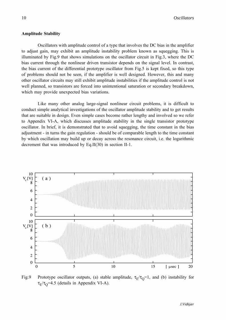
Amplitude Stability
Oscillators with amplitude control of a type that involves the DC bias in the amplifier
Fig.9 Prototype oscillator outputs, (a) stable amplitude, τE/τQ=1, and (b) instability forτE/τQ=4.5 (details in Appendix VI-A).
to adjust gain, may exhibit an amplitude instability problem known as squegging. This isilluminated by Fig.9 that shows simulations on the oscillator circuit in Fig.3, where the DCbias current through the nonlinear driven transistor depends on the signal level. In contrast,the bias current of the differential prototype oscillator from Fig.5 is kept fixed, so this typeof problems should not be seen, if the amplifier is well designed. However, this and manyother oscillator circuits may still exhibit amplitude instabilities if the amplitude control is notwell planned, so transistors are forced into unintentional saturation or secondary breakdown,which may provide unexpected bias variations.
Like many other analog large-signal nonlinear circuit problems, it is difficult toconduct simple analytical investigations of the oscillator amplitude stability and to get resultsthat are suitable in design. Even simple cases become rather lengthy and involved so we referto Appendix VI-A, which discusses amplitude stability in the single transistor prototypeoscillator. In brief, it is demonstrated that to avoid squegging, the time constant in the biasadjustment - in turns the gain regulation - should be of comparable length to the time constantby which oscillation may build up or decay across the resonance circuit, i.e. the logarithmicdecrement that was introduced by Eq.II(30) in section II-1.
J.Vidkjær

11VI-1 Oscillator Basics
Oscillator Noise
Noise in oscillators manifests itself by an output spectrum that is not just a single line
Fig.10 Spectrum analyzer output from an oscillator. (Δf) is called the single sidebandnoise function. The widening of the spectrum around the center frequency is causedby noise.
but gives spectrum that widens apart from the center frequency as sketched in Fig.10. Weshall consider a simplified, partly empirical oscillator noise model, the so-called Leeson model[5], in this section. The model explains major noise properties and parameter dependenciesin experimental observations. The prototype oscillators from above are used to make thesimplified model plausible, but due to the nonlinear amplifier operation in an oscillator, thedetailed theoretical treatment of oscillator noise is complex and far beyond our scope. To gofurther, the interested reader should consult ref´s [6] or [7],sec.10.4.
Fig.11 Oscillator block-scheme for noise description.
The oscillator noise model is obtained in two steps. It is assumed that the noise canbe ascribed to the amplifier and represented by an equivalent input noise. First the relationshipbetween input and output noise spectra are calculated. Second, the nature and shape of theactual noise source spectra are incorporated.
Fig.11 repeats out initial block scheme representation of an oscillator. Applied to theprototype oscillator, the subdivision from Eq.(10) implies that the frequency selective feed-back network holds lossless components L and C only. All noise sources are represented bythe input noise voltage Vn,in. When the oscillator is running, the output contains both thedesired constant amplitude sinusoidal voltage Vocosω0t and noise components Vn,out, which
J.Vidkjær

12 Oscillators
originates from Vn,in. We suppose initially that all noise voltages are so small that they haveno influence on the amplitude control and, furthermore, that the oscillations have settled attheir final amplitude. Barkhausen’s requirement expressed through Eqs.(7) to (9) is
Invoking this condition, and using the b-function from Eq.(6), the noise voltage transfer
(21)
function becomes
where the frequency dependency is kept in β(ω). Going to noise spectra, the power spectral
(22)
densities at the input and output of the oscillator, when normalized with respect to the sameimpedance levels, are related by the absolute square of the voltage transfer function. If Sn,in(ω)is the input noise spectrum and Sn,out(ω) the corresponding output spectrum, we have
Around the resonance frequency ω0 we may replace the Qlβ product by its narrowband
(23)
approximation, which was introduced in section II-3. Thereby, we get expressions for thespectra in terms of the frequency deviation Δω from resonance,
Here W3dB is the usual 3dB bandwidth of the resonance circuit. We compare to only half of
(24)
Fig.12 Asymptotic transfer characteristic between input and output noise spectra in theoscillator block-scheme from Fig.11.
that because the bandwidth is defined as the distance between the 3dB point above and below
J.Vidkjær

13VI-1 Oscillator Basics
ω0 with Δω being either positive or negative. A break-point characteristic corresponding tothe transfer function is shown in Fig.12. It goes towards infinity when the frequency isapproaching the oscillator frequency but this was expectable as Barkhausen´s condition impliesinfinite gain at resonance frequency if the oscillator is considered as an feedback amplifier.
Oscillators noise is commonly separated into amplitude noise, vna(t), and phase noiseφn(t). The total oscillator output voltage is expressed
The last approximation assumes a phase-noise much smaller than one radian, so its cosine
(25)
function approximates one and the sine function approximate the phase-noise itself. Comparedwith an additive noise description
it is seen, that the last line in Eq.(25) is equivalent to an in-phase and quadrature resolution
(26)
of the additive noise around the oscillator frequency. Starting from common additive gaussiannoise sources, the noise power divides evenly between the in-phase and the quadrature termsin such a resolution. Dealing with oscillator noise, it is custom to disregard the amplitude termsince the oscillator circuit is designed to keep the amplitude constant and, furthermore, theoutput commonly undergoes further limiting before it is applied in critical application. Weshall follow this simplifying approach below.
Suppose the noise in the oscillator amplifier is white thermal noise. In equivalencyto small-signal two-port noise characterization, the portion of the input noise spectrum thataccounts for phase noise may be written in the form
where Feff is an effective noise figure that describes the amplifier under large signal sinusoidal
(27)
excitation, k is Boltzman’s constant, and To is the reference temperature for noise in Kelvin.Since this spectrum is flat, the result is directly transferred to the so-called single-sidebandphase noise spectrum (Δf). It is a spectrum like Fig.10, which is read directly from aspectrum analyzer using 1Hz resolution bandwidth. It gives the power spectral density relativeto the sinusoidal output power Po, which is proportional to ½Vo
2. Δf denotes the differencein frequency from the oscillator signal. The simple noise model assumes a spectrum that issymmetric around the oscillator frequency. To fully include the power in one hertz bandwidth
J.Vidkjær

14 Oscillators
at frequency distance |Δf| from the oscillator frequency we must include twice the value of(Δf), where
In dB scale, 10 log (Δf) is referred to as dBc, decibels over carrier. Clearly this spectrum is
(28)
a scaled version of the transfer characteristic from Eq.(24) since the input spectrum is flat.However, it was discussed in the flicker noise paragraph of section IV-1, Eq.IV(21), that the1/f noise in electron devices are transferred to the frequency range around a large sinusoidaldriving signal. We have the same driving situation by the last term in Eq.(25), so includingflicker noise, the input spectrum gets a 1/f term and the output may be written,
where the characteristic frequency fa is a flicker noise parameter. The expression is the final
(29)
form of the Leeson oscillator model, which gets two asymptotic appearances dependent onwhether fa is smaller or larger than half the 3dB bandwidth of the resonance circuit in theoscillator. These two cases are summarized in Fig.13 (a) and (b) respectively.
Fig.13 Asymptotic single sideband oscillator noise characteristics where in (a) resonator half-bandwidth exceeds the flicker noise bandwidth and vice versa in (b).
J.Vidkjær

15
VI-2 Oscillator Circuits
The number of oscillator circuits that are used in practice is overwhelming, and it isimpossible here to give a broad coverage. Therefore, the treatments below serves the purposesof both presenting a few common oscillator configurations and of presenting analyticaltechniques that also may be useful with other oscillator circuits. Furthermore, we shall pointout a few important design aspects.
LC Oscillators
Circuits intended for sinusoidal outputs up to a few GHz in frequency may be build
Fig.14 LC oscillator example. The equivalent circuit in (b) includes the large signal transis-tor model in Fig.15. Resistors RA, RB, and RC may represent losses and/or loads.
using inductors and capacitors as tuning elements - the so called LC-oscillators. Comparedwith the prototype circuits in the forgoing section, the circuits we consider here are simplerin the sense that the required feed-back is inherent in the circuit topology. However, therequirements for oscillations are not identified as easily as it could be done in the transformerfeed-back circuits.
Fig.15 Transistor equivalent circuit. Under large signal conditions, the components applyto the fundamental frequency and they depend on the signal levels at the input andoutput ports.
One family of practical oscillator circuits, which we shall call the Colpit’s family, isbased on the circuit topology in Fig.14(a), where capacitors CA, CB, and inductor LC are
J.Vidkjær

16 Oscillators
supposed to be the dominant tuning elements. The transistor symbol in the diagram representsthe transistor including biasing arrangements under large signal operation. At this level ofapproximation the transistor may be either bipolar or FET types. In the foregoing analysis ofthe prototype oscillator we used the simple, ohmic large signal transistor model in Fig.3(c).With caution, this model may be extended to incorporate capacitive effects, so the transistoris described by the large signal model in Fig.15. Like the simpler model, the new componentsCπ1, Cμ1, Co1, and Ro1 apply to the fundamental frequency and depend on the voltages acrossthe transistor, so the quantities are not deductible in details from the small-signal data thatcommonly are provided in data-sheets. However, it is seen in the equivalent circuit ofFig.14(b), which is cast in a form that facilitates open loop gain calculations, that all elementsin the transistor are shunted by external components. Resistors RA, RB, and RC mightrepresent possible capacitor and inductor losses, external loads, or both. External componentsare expected to play the dominant role, since it is a common design objective to keep theoscillator insensitive to transistor parameter variations. For that purpose even crude approxi-mations to the large signal transistor parameters suffices. Note finally that with exception ofpossible biasing contributions we may often disregard the transistor resistors Rπ1 in FET andRo1 in bipolar transistor calculations.
Fig.16 Circuit structure and signal flow-graph for calculating the open loop gain in theoscillator equivalent circuit from Fig.14(b).
Like the previous oscillator prototype analysis, the condition for oscillation is that theopen loop gain in the circuit equals one in size and zero in phase. The structure of the circuitin Fig.14(b) has a form that is given by Fig.16. In general terms the open loop voltage gain,Aol , and the criterion for oscillation are expressed,
Inserting components
(30)
(31)
and taking real and imaginary parts in Eq.(31), the condition splits into the following two
(32)
conditions that must be simultaneously met,
J.Vidkjær

17VI-2 Oscillator Circuits
In details, the admittances to be inserted in the two requests are
(33)
(34)
Inserting these expressions, the two requests constitutes a system of equations that determines
(35)
the frequency of oscillation ω0 and the large signal transconductance Gm, which is necessaryto maintain oscillations. Besides these two significant quantities, we shall often require the Q-factor - the loaded Q - of the open-loop gain since it determines the important properties offrequency stability and noise in the oscillator. A direct way of conducting the calculation isto find the derivative of phase with respect to angular frequency in loop gain and then,cf.Eq.(20), get the Q-factor from the relationship
Finally, the loading of the transistor might be required to check whether or not a device is
(36)
adequate in a given application. According to Fig.16 and Eq.(30), the load impedance seenfrom the port of the tranconductance current generator is given through
The oscillator circuit topology in Fig.14(a) contains no ground node and the corre-
(37)
(38)
sponding criteria for oscillations are independent of which one of the transistor terminal thatis set to - or taken as - the signal ground. Distinctions between the different ways of ground-ing is made from practical reasons since the literature often refer to circuits named after their
J.Vidkjær

18 Oscillators
inventors. The tree possibilities with the present topology are summarized in Fig.17. They are
Fig.17 Colpitt’s (a), Pierce (b), and Seiler (c) oscillators. They are deduced from Fig.14 bygrounding base, emitter, or collector - gate, source, or drain - respectively.
known as Colpitts, Pierce and Seiler oscillators. Considering the figures it should still be keptin mind that the transistor symbol represents a transistor under large signal operation, eitherbipolar’s or FET’s. It includes the type of bias network that is required to reduce transcon-ductance and in turn stabilize the oscillation amplitude. Note also that the output indicationsin the figures are suggestions as any non-grounded node in the circuit has an oscillatingvoltage component. Which one to use depends on the application since the different nodesdiffer with respect to distortion, noise, and output power capabilities if they are loaded.
Simplified Analysis of Colpitts Family of Oscillators
To illuminate and to make practical use of the conditions from Eqs.(33) to (38), weconsider a few simplified situations where it is assumed that the transistor feed-back capaci-tance is negligible, so the susceptances are in all cases given by
Assume for a moment that there were no resistive losses in the circuit, i.e.
(39)
In this hypothetical situation, the real part condition from Eq.(33) provides
(40)
(41)
J.Vidkjær

19VI-2 Oscillator Circuits
As seen, the frequency of oscillation ω0 becomes the resonance frequency ω00 of an idealresonance circuit made of inductor LC and the series connection of capacitances Ca and Cb.The corresponding imaginary part condition implies
which means that once the oscillations have started, there are no need for an active element
(42)
to compensate resistive losses, since they are absent in this particular case. Below we shallinclude losses and find the corresponding transconductance requirements. Since the analysisbecomes involved with more than one resistive component, we assume one dominant resistivecomponent in the initial calculations. Afterwards, the results may be slightly adjusted tocorrect for less significant losses.
Case 1 in load resistor placement
If the only ohmic component resides across the transistor output terminals the
Fig.18 Equivalent circuit for the oscillator loop gain with simplifying assumptions, notransistor feed-back and resistive loading across the transistor output terminals only.
equivalent diagram becomes the one shown in Fig.18. The conductances are
The real-part condition and, consequently, the frequency of oscillation remains unaltered from
(43)
the results in Eq.(41). The imaginary part condition now provides
i.e. is an expression for the size of the transconductance that the transistor must approach
(44)
when oscillations build up to the desired amplitude. Including the oscillation frequency fromEq.(41), we get
(45)
J.Vidkjær

20 Oscillators
To find the Q-factor of the open-loop gain, direct insertion of Eq.(43) into Eq.(30) gives
At the oscillation frequency ω=ω0 this angle should vanish and direct substitution from
(46)
(47)
Eq.(41) reveals that the expression in brackets becomes zero. The derivative with respect toangular frequency at ω0 now develops
and the corresponding Q-factor becomes
(48)
Here we have demonstrated a direct approach to the Q-factor calculation. It may seem
(49)
Fig.19 Parallel to series to parallel conversion used for estimating the Q-factor in theoscillator from Fig.18.
cumbersome, but it has the virtue that we don’t need to identify and refer all ohmic losses toa particular resonance circuit. In the present simplified case with only one resistor we may,however, easily check the result as we have already seen, that the oscillating frequency is set
by resonance between inductor LC and the series connection of Ca and Cb. Since Ra appearacross Ca, its equivalent series resistance Rser in Fig.19(b) is determined by this capacitor, butit is also the total series loss in resonance with the series connected capacitors. By parallel-to-series transformations according to Eq.(III-59), we get
J.Vidkjær

21VI-2 Oscillator Circuits
i.e. the same result as before. Clearly we would also get this result - which is included here
(50)
for future reference - by transforming to parallel form like Fig.19(c), where
The voltage gain around the transistor and the transistor load are calculated by Eqs.(37), (38),
(51)
and (45) to yield
Case 2 in load resistor placement
(52)
Fig.20 Equivalent circuit for the oscillator loop gain with simplifying assumptions, notransistor feed-back and resistive loading across the transistor input terminals only.
The second simplified case we consider has resistive loading across the transistorinput terminalsas seen in Fig.20. Here the simplified analysis is based on the conductances,
Again, the real-part condition and the frequency of oscillation remain unaltered from the
(53)
results in Eq.(41). The imaginary part condition provides
J.Vidkjær

22 Oscillators
Compared with Fig.19(a), a-terms and b-terms have changed roles, so in analogy to Eq.(50),
(54)
the Q-factor with resistive losses across the transistor input port becomes
Finally, the voltage gain and the load at the frequency of oscillation from Eqs.(37) and (38)
(55)
simplify to
In contrast to the previous case, gain and load impedance now get small imaginary compo-
(56)
(57)
nents as a consequence of the reactive separation between the transistor transconductance andthe ohmic load. However, the higher Rb, the higher Q, and the less significant become theimaginary components.
Case 3 in load resistor placement
The final simplified case to consider is the one where the load and losses connectacross the inductance LC as indicated by Fig.21. There are no components from the transistorequivalent circuit in this position, so the conductances are given by
In this case, the real part and the imaginary part conditions from Eqs.(33) and (34) are no
(58)
longer independent, since
The last equation is similar to
(59)
J.Vidkjær

23VI-2 Oscillator Circuits
which - when inserted in the real part condition - provides
Fig.21 Equivalent circuit for the oscillator loop gain with simplifying assumptions, notransistor feed-back and resistive loading across the inductor only.
(60)
Here we have used the resonance frequency ω00 defined in Eq.(41) and the quality factor QL
(61)
for the inductor at resonance ,
It is seen that the larger QL, the closer comes the oscillator frequency to the resonance
(62)
frequency ω00. Since the only resistive loss is provided by RC, the inductor Q-factor QLbecomes also the Q-factor for the oscillator. Inserting the oscillator frequency into Eq.(60)gives the necessary transconductance,
The voltage gain and the transistor load become
(63)
(64)
(65)
J.Vidkjær

24 Oscillators
Arbitrary resistor placements
Fig.22 Oscillator equivalent circuit. Parallel resistance Rp accounts for all resistive lossesin the circuit.
A unified approach to the three cases above can be achieved through Fig.22, whereresonance circuit and capacitive transformer properties of the oscillator are emphasized. Thetransformation ratio is, cf. sec.II-6,
With high Q-factors, the reactive currents in LC and the series connection of Ca and Cb at
(66)
resonance are large compared to the loss currents through Rp or, equivalently the transistorload, Ztr0, which may be expressed
Accordingly, the capacitive current Ica is nearly equal to Icb, and the voltage ratio across the
(67)
two capacitors becomes inversely proportional to the capacitances,
To maintain oscillations the loop gain must be one so voltage Vb1 across Cb1 in the diagram
(68)
equals the control voltage for transconductance Gm. We get
where the last expression sets the requirement to Gm. With Rp set to RC it is seen that the Gm
(69)
we have just derived corresponds to the value in Eq.(63) as expected, since the diagram inFig.22 is a reorganization of the diagram in Fig.21. More noticeably is the observation that
J.Vidkjær

25VI-2 Oscillator Circuits
if we replace Rp with the equivalent parallel resistor Rpar from Eq.(51) for losses that areconcentrated across the transistor output port, we get
which is the same as the Gm request in Eq.(45). Had we made a similar derivation from
(70)
Eq.(69) in the case where ohmic losses are concentrated across the transistor input terminallike in Fig.20, we would have obtained the transconductance value in Eq.(54). Thus weestimate Gm correctly from different loss components taken one by one if they are transformedto the parallel equivalent resistance Rpar. This fact suggests that the joint effect upon Gm ofmore losses from different locations in the circuit may be calculated from a parallel connectionof their equivalent parallel resistances. We may even use series-to-parallel transformation toconvert all loss contributions to one of the special case that were considered if it suits ourneed for making other design calculation. Such approaches are much simpler than an attemptto solve the corresponding real and imaginary part condition simultaneously. We shalldemonstrate them in the following two examples.
Example VI-2-1 ( Seiler type LC oscillator )
The oscillator circuit in Fig.23(a) is a Seiler circuit where the transistor is current
Fig.23 Seiler oscillator. With exception of current bias details, part (a) shows the circuitdiagram while part (b) shows the functional diagram that is used in the design.
biased, presently without showing details on how this is made in practice. The tuning capacitoracross the transistor output port is made of a series connection, CA1 and CA2, which trans-forms the required load resistance RL to a larger equivalent transistor load resistance, Ra, asindicated by the functional diagram in Fig.23(b). This way we get more suitable componentvalues and better utilization of the battery supply than a direct connection of the load to thetransistor would provide. Resistors Rb1 and Rb2 are base bias resistors and Ccp1 is a decoup-ling capacitor. The main requirements to the circuit are
J.Vidkjær

26 Oscillators
- frequency, f0 = 300 MHz,- output power, Pout = 2 mW in RL=50Ω,- loaded Q-factor, Ql > 20,- gain reduction at nominal output, Gm:gm ∼ 1:2.5
It is furthermore assumed that the transistor requires Vce > Vce,min=0.5V to prevent saturationeffects and that it has a forward current gain βf = 50, equivalently αf = 0.98.
We shall assume that the load Ra is the only resistive component in the oscillatorequivalent circuit, so the design corresponds to the first case that was considered above inconjunction with the equivalent circuit in Fig.18. To find the equivalent load resistor Raassume that the transistor output voltage swing Va1 is half the battery voltage minus two timesthe minimum voltage Vce,min, where the first count comes from transistor Q1, the second countleaves room for a transistor in the bias current generator. With Va1 fixed, the correspondingload resistor is calculated from the output power requirement,
According to Eq.(5-100) and Figure 5-44 in chapter 5, a 1:2.5 reduction in gain when
(71)
(72)
the oscillations grow up requires the final drive level xmax, which is normalized with respectto the thermal voltage Vt=kT/q∼25mV, where
To find the capacitances Ca and Cb, Eqs.(50) and (52) provide
(73)
The tuning condition follows from Eq.(41), which gives
(74)
(75)
J.Vidkjær

27VI-2 Oscillator Circuits
Impedance transformation from RL to Ra implies the transformation ratio
(76)
so the two capacitances that connect to Ca become
(77)
To keep the oscillations running, the final large signal conductance is given by Eq.(45),
(78)
The DC bias current IEE is now calculated from the current gain reduction of 1:2.5. We get
(79)
The final step in the design is to fix the base biasing and to implement the IEE current source.
(80)
In agreement with the initial emitter oscillator amplitude calculation in Eq.(71), the meanemitter voltage Ve0 is given by
When oscillations grow up and the transistor is forced into class C operation, the mean base
(81)
emitter voltage will be slightly reduced from its initial DC value, which commonly is in therange of Vbe0=0.65V. We ignore this adjustment here since the effect is small with currentbiasing, so the base DC-bias voltage should be Vb0=Vbe0+Ve0=2.4V. Choosing the commonDC current Ibr through Rb1 and Rb2 to be approximately ten times the base dc current, whichis Ib0∼IEE/βf=0.04mA, i.e. Ibr=0.4mA, the bias resistors become
J.Vidkjær

28 Oscillators
The decoupling capacitor Ccp1 should be chosen so its reactance at the oscillation frequency
(82)
is small compared to both the parallel connection of Rb1 and Rb2 and to the reactance of LC.The last requirement is the strongest since Rb1 Rb2∼1.9kΩ while ω0LC=Ra/Q=20Ω. Followingthe results from Eq.(76), we chose
Current biasing may ideally be implemented by a current mirror as sketched in Fig.24(a). If
(83)
transistors Q2 and Q3 are identical, Rb3 should be adjusted so that its current equals the biascurrent IEE. Less ideally, current biasing may be provided simply by a large resistor as showin Fig.24(b). With the DC currents and voltages from above, the resister should be
Although this value is significantly larger than the equivalent load resistor Ra, which REE is
(84)
connected across, the power loss at the oscillation frequency in REE cannot be ignoredcompared to the output requirement. If this simpler solution is chosen, the design should beadjusted to compensate for the additional loss.
Example VI-2-1 end
Fig.24 Current bias methods for the Seiler oscillator using, (a), a current mirror or, (b), alarge resistor REE.
J.Vidkjær
29VI-2 Oscillator Circuits
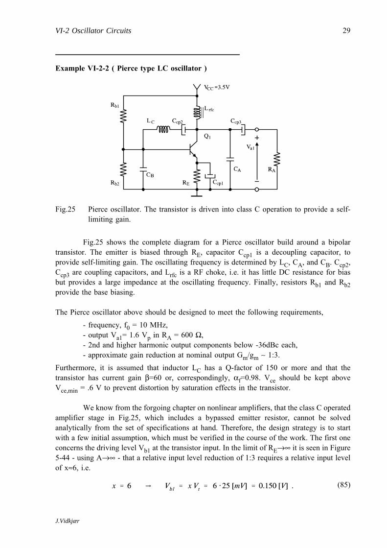
Example VI-2-2 ( Pierce type LC oscillator )
Fig.25 shows the complete diagram for a Pierce oscillator build around a bipolar
Fig.25 Pierce oscillator. The transistor is driven into class C operation to provide a self-limiting gain.
transistor. The emitter is biased through RE, capacitor Ccp1 is a decoupling capacitor, toprovide self-limiting gain. The oscillating frequency is determined by LC, CA, and CB. Ccp2,Ccp3 are coupling capacitors, and Lrfc is a RF choke, i.e. it has little DC resistance for biasbut provides a large impedance at the oscillating frequency. Finally, resistors Rb1 and Rb2provide the base biasing.
The Pierce oscillator above should be designed to meet the following requirements,
- frequency, f0 = 10 MHz,- output Va1= 1.6 Vp in RA = 600 Ω,- 2nd and higher harmonic output components below -36dBc each,- approximate gain reduction at nominal output Gm/gm ∼ 1:3.
Furthermore, it is assumed that inductor LC has a Q-factor of 150 or more and that thetransistor has current gain β=60 or, correspondingly, αf=0.98. Vce should be kept aboveVce,min = .6 V to prevent distortion by saturation effects in the transistor.
We know from the forgoing chapter on nonlinear amplifiers, that the class C operatedamplifier stage in Fig.25, which includes a bypassed emitter resistor, cannot be solvedanalytically from the set of specifications at hand. Therefore, the design strategy is to startwith a few initial assumption, which must be verified in the course of the work. The first oneconcerns the driving level Vb1 at the transistor input. In the limit of RE→∞ it is seen in Figure5-44 - using A→∞ - that a relative input level reduction of 1:3 requires a relative input levelof x≈6, i.e.
(85)
J.Vidkjær

30 Oscillators
According to the discussion of the bipolar parallel tuned amplifier on page 19 in chapter 5,we see from Figure 5-16 that for a given argument x - the second order modified Besselfunction is greater than third and any higher order functions. Since the harmonic componentsin the collector current over the fundamental frequency component is the ratio of the cor-responding ordered modified Bessel function over the 1st order function, the 2nd harmoniccomponent introduces the largest distortion and is the one to be used in the design. UsingFigure 5-16 we get
The fundamental frequency output voltage component corresponds to resonance in the
(86)
resonance circuit containing LC and the series connection of Ca and Cb. The collector loadimpedance is a downscaled version of this circuit which at resonance is Ztr0. The correspond-ing impedance at n times the resonance frequency is
where Ql is the total loaded Q-factor for the resonance circuit. Imposing the distortion
(87)
requirements for 2nd order harmonic components, we get
This Q-factor is considerably smaller than the Q-factor that represents losses in inductor LC,
(88)
the internal losses, and load resistor RA is supposed to contribute most significantly to thetotal loss in the circuit. Other contributions to the internal losses come from the transistorinput impedance and biasing networks, so we design with an internal Q-factor that is some-what lower than QL, say Qint=120, and verify that we stay within specifications afterwards.As RA is still the most significant loss, it is natural to use our first special case as foundationfor the design, i.e. use the circuit in Fig.18 and the pertinent equations. However, we shouldfirst modify the load to a resistor RA’ that incorporates the internal losses. The latter arerepresented by a resistor Rint across RA. Following the terminology that was introduced insection II-4, the Q-factor corresponding to RA may be referred to as the external Q-factor,Qext. Due to the parallel connections and the proportionality between Q-factors and parallelresistors we have
J.Vidkjær

31VI-2 Oscillator Circuits
The equivalent intrinsic loss resistance to be parallelled across RA has the size
(89)
Using Eqs.(50) and (52) we get
(90)
The corresponding inductor is given by
(91)
When the circuit oscillates with the assumed output voltage swing of 1.6 Vp, the correspond-
(92)
ing fundamental frequency collector current component is
With a relative driving level of x=6, the corresponding collector and emitter DC currents with
(93)
ongoing oscillations are
(94)
J.Vidkjær
32 Oscillators
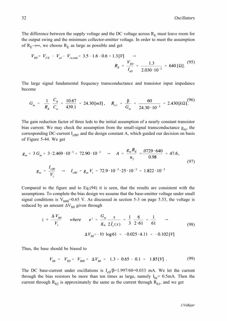
The difference between the supply voltage and the DC voltage across RE must leave room forthe output swing and the minimum collector-emitter voltage. In order to meet the assumptionof RE→∞, we choose RE as large as possible and get
The large signal fundamental frequency transconductance and transistor input impedance
(95)
become
The gain reduction factor of three leds to the initial assumption of a nearly constant transistor
(96)
bias current. We may check the assumption from the small-signal transconductance gm, thecorresponding DC-current Ic00, and the design constant A, which guided our decision on basisof Figure 5-44. We get
Compared to the figure and to Eq.(94) it is seen, that the results are consistent with the
(97)
assumptions. To complete the bias design we assume that the base-emitter voltage under smallsignal conditions is Vb00=0.65 V. As discussed in section 5-3 on page 5.53, the voltage isreduced by an amount ΔVb0 given through
Thus, the base should be biased to
(98)
The DC base-current under oscillations is Ic0/β=1.997/60=0.033 mA. We let the current
(99)
through the bias resistors be more than ten times as large, namely Ibr= 0.5mA. Then thecurrent through Rb2 is approximately the same as the current through Rb1, and we get
J.Vidkjær

33VI-2 Oscillator Circuits
The parallel connection of Rb1, Rb2, and the large signal input resistance Rπ1 from Eq.(96)
(100)
contributes to Q-factor. Since they are placed across capacitor Cb, we get
This is a high Q-factor compared to the assumed value of Qint = 120, so the transistor input
(101)
and biasing resistors contribute nothing to the losses compared with the inductor loss. Theparallel loss Rint comes from tuning inductor LC has QL=150, and a corresponding parallelresistance,
so within the design above, there is room for a loss introduced by the RF choke Lrcf. Its
(102)
parallel resistance may go down to
To complete the design, coupling capacitor Ccp2 should not contribute to the tuning so it must
(103)
be large compared Cser from Eq.(92), say Ccp2=100nF. The reactance of coupling capacitorCcp3 should be small compared to the load resistor RA, i.e.
(104)
Finally Ccp1 must bypass RE. Since the time constant of τE=RECcp1 directly influence the gainregulation in Gm, the capacitance should not be chosen too high in order to avoid the squeg-ging type of amplitude instability. According to the discussion in Appendix VI-A, a safechoise is to set the time constant τE equal to the logarithmic decrement of the resonancecircuit. Thereby we get
J.Vidkjær

34 Oscillators
Capacitor Ccp1 controls the time constant in the gain control of the transistor under large
(105)
signal operations in a manner that can be foreseen. However, the two coupling capacitors Ccp2and Ccp3 might also contributes to this control, but it is difficult to work out the detailsanalytically. The values that were calculated formerly did not incorporate any stability con-cerns, so we must be prepared to adjust the capacitor values when the circuit is build inpractice or simulated to check performance. The latter is done in Fig.26, and there are noindications of amplitude instabilities in this design.
Fig.26 Build-up of oscillations in the Pierce oscillator from Fig.25 using the componentvalues that were calculated in the example.
Example VI-2-2 end
J.Vidkjær

35
VI-3 Crystal Oscillators
Quartz is a piezo-electrical material where mechanical deformations cause voltagedifferences across distinct surfaces and visa versa. A small sheet of quartz exhibits mechanicalresonant modes that depend on its geometry, the orientation of the cut compared to the crystalaxes, and the type of vibration engaged like compression, torsion, or shear oscillations. Withtwo electrodes evaporated on the crystal, we get a component that typically has an impedancepattern as sketched in Fig.27. It shows pronounced resonances at the fundamental frequencyand odd numbered overtones. Even numbered mechanical modes make no resultant displace-ment of the electrodes and cannot be exited electrically. Between dominant modes spuriousresonances from other type of vibrations may be observed. Mechanical resonances havegenerally high Q-values and combined with excellent temperature stability and long-term agingproperties, the quartz crystal is widely used as the frequency controlling element in oscillatorsthat operates within close tolerances in the frequency range of .1 to approximately 350 MHz.
Crystal Equivalent Circuits
Fig.27 Impedance magnitude of quartz crystal with strong resonances at the fundamentalmode and odd overtones. In between spurious resonances from other types ofvibrations may be observed.
From an electrical point of view, the quartz crystal may be represented by the
Fig.28 Electrical equivalent circuit of a quarts crystal. (a) includes all modes and (b)suffices for narrowband calculations with a particular mode. (c) is a redrawing of(b) emphasizing its parallel resonance.
equivalent circuit in Fig.28(a), where the capacitor C0 is the capacitance between the elec-trodes if there were no mechanical resonances. Each series resonant circuit Ci, Li, ri, representa mechanical mode that may be excited by the piezo-electric effect. Commonly crystals are
J.Vidkjær

36 Oscillators
optimized with respect to a particular mode that is recommended for circuit design. In thefrequency range around the selected mode, it suffices to consider an equivalent circuitcomposed of only the electrode capacitance and the series circuit associated with the modein question. This circuit is shown in Fig.28(b) and has the impedance,
The last expression introduces the series resonance frequency ω0 and the corresponding Q-
(106)
factor of the series circuit,
Setting the numerator and the denominator in Eq.(106) equal to zero and solving for s, we get
(107)
the impedance zeros and poles,
Practical data justify the approximations, which imply large Q-factors. Extremely high Q´s are
(108)
obtainable with crystals - up to 100000 - so the small losses get no influence on the imaginaryparts of poles and zeros. Moreover, the electrode capacitance is much greater than anyresonator capacitance and we may use the estimation
in the last expression, which determines a parallel resonance frequency - sometimes also called
(109)
the antiresonance frequency - ωp, where
The series resonance is responsible for the zero of the impedance function. In conjunction with
(110)
the electrode capacitance Co it also provides the pole that implies the parallel resonance,which may be viewed upon like a parallel resonant circuit with capacitive transformation asshown in Fig.28(c).
J.Vidkjær

37VI-3 Crystal Oscillators
Fig.29 Impedance in magnitude, phase and in real, imaginary forms for the crystal examplein Eq.(111). Note the logarithmic impedance scales and the sign indications for theimaginary part of the impedance.
(111)
Due to the existence of both series and parallel resonances there may be two waysof utilizing a crystal in an oscillator, either as a low impedance devices in series resonancearound ω0 or as a high, inductive impedance device in parallel resonance up to ωp. Thepossibilities are readily seen in Fig.29, which shows a calculation of the impedance functionfrom Eq.(106) based on the crystal data in Eq.(111). With practical data, the series and parallelresonances are closely spaced in frequency. In this case, however, the distance is still largecompared to the real part of poles and zeros, so the two resonances are clearly distinguishable.The separation may be expressed through the following figure of merit M,
J.Vidkjær

38 Oscillators
where the distance ωp-ω0 is given through Eq.(110).
Fig.30 Pole-zero pattern for a single resonant mode in the crystal. The encircled region isshown in (b) for series and (c) for parallel resonances and indicate phasor assump-tions in narrowband approximations.
(112)
The two types of resonances in Fig.29 show both the steep phase characteristic thatis required for good frequency stability. We chose between them in design by letting the restof the circuit meet oscillation criteria with either high or low impedance levels. Crystalsoperated in fundamental mode have usually high M values. Therefore, the impedance may benarrowband approximated around either ω0 or ωp using the method that was applied to LCtuned circuits in section II-3. With known poles and zeros the crystal impedance is expressed
The pole-zero pattern for the crystal is shown in Fig.30(a) while Fig.30(b) and (c) indicate the
(113)
geometry to be used in the narrowband approximation. Notice that the figures are not drawnto scale as the pole and zero distances to the imaginary axis should be much smaller comparedto their mutual spacings. With the assumptions in the figures we get
J.Vidkjær
39VI-3 Crystal Oscillators
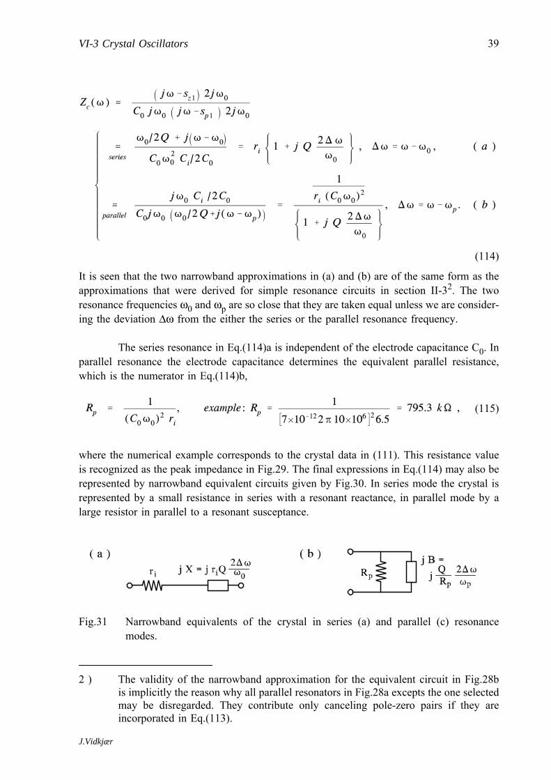
It is seen that the two narrowband approximations in (a) and (b) are of the same form as the
(114)
approximations that were derived for simple resonance circuits in section II-32. The tworesonance frequencies ω0 and ωp are so close that they are taken equal unless we are consider-ing the deviation Δω from the either the series or the parallel resonance frequency.
The series resonance in Eq.(114)a is independent of the electrode capacitance C0. Inparallel resonance the electrode capacitance determines the equivalent parallel resistance,which is the numerator in Eq.(114)b,
where the numerical example corresponds to the crystal data in (111). This resistance value
(115)
is recognized as the peak impedance in Fig.29. The final expressions in Eq.(114) may also berepresented by narrowband equivalent circuits given by Fig.30. In series mode the crystal isrepresented by a small resistance in series with a resonant reactance, in parallel mode by alarge resistor in parallel to a resonant susceptance.
Fig.31 Narrowband equivalents of the crystal in series (a) and parallel (c) resonancemodes.
2 ) The validity of the narrowband approximation for the equivalent circuit in Fig.28bis implicitly the reason why all parallel resonators in Fig.28a excepts the one selectedmay be disregarded. They contribute only canceling pole-zero pairs if they areincorporated in Eq.(113).
J.Vidkjær
40 Oscillators
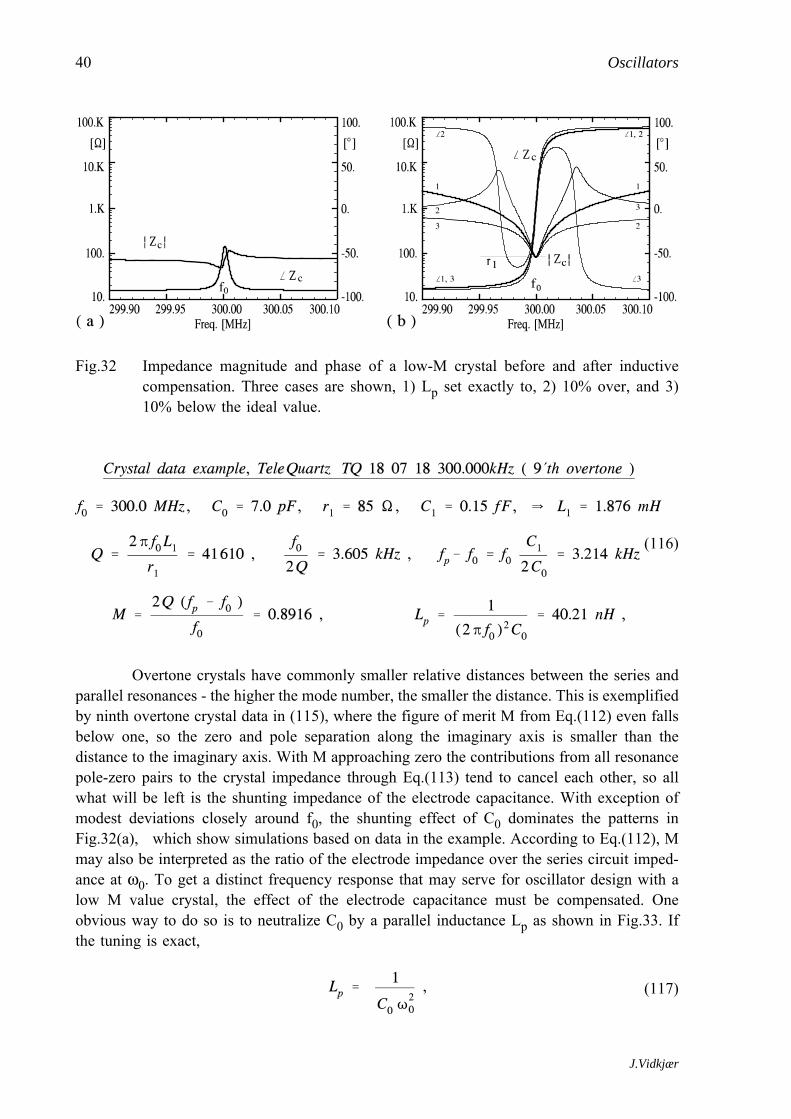
Overtone crystals have commonly smaller relative distances between the series and
Fig.32 Impedance magnitude and phase of a low-M crystal before and after inductivecompensation. Three cases are shown, 1) Lp set exactly to, 2) 10% over, and 3)10% below the ideal value.
(116)
parallel resonances - the higher the mode number, the smaller the distance. This is exemplifiedby ninth overtone crystal data in (115), where the figure of merit M from Eq.(112) even fallsbelow one, so the zero and pole separation along the imaginary axis is smaller than thedistance to the imaginary axis. With M approaching zero the contributions from all resonancepole-zero pairs to the crystal impedance through Eq.(113) tend to cancel each other, so allwhat will be left is the shunting impedance of the electrode capacitance. With exception ofmodest deviations closely around f0, the shunting effect of C0 dominates the patterns inFig.32(a), which show simulations based on data in the example. According to Eq.(112), Mmay also be interpreted as the ratio of the electrode impedance over the series circuit imped-ance at ω0. To get a distinct frequency response that may serve for oscillator design with alow M value crystal, the effect of the electrode capacitance must be compensated. Oneobvious way to do so is to neutralize C0 by a parallel inductance Lp as shown in Fig.33. Ifthe tuning is exact,
(117)
J.Vidkjær

41VI-3 Crystal Oscillators
only the series resonant circuit remains and may be used as an equivalent circuit around ω0.
Fig.33 Compensation of electrode capacitance by a parallel inductance in a low-M crystal.
However, a less precise compensation still works if the impedance of C0 paralleled by Lp islarge compared to ri. Then the series resonance pattern - distinct magnitude minimum andsteep rise in phase - prevails as seen in the characteristics of Fig.32(b), where all examplescoincide around f0.
Loading and Driving Crystals
To benefit from crystals in oscillator design, it is important to keep the Q-factor high.Compared to the Q-factor of the crystal itself, which in the present context often is referredto as the unloaded Q, some reductions are unavoidable when the crystal is connected to theremaining part of the oscillator circuit, which contains transistor impedances, biasing networks,and the external load. If the losses transform to a series resistor rL in a crystal that is used inseries mode, Fig.34(a), the resultant Q-factor is the one we get by adding the external resistorto the internal resistor in Eq.(107), i.e.
Correspondingly, if the external losses may be represented by a parallel resistance RL to a
(118)
crystal that is operated in parallel mode, the resultant Q-factor is the one we get from parallel-ling the external resistance to the parallel resistance Rp, Eq.(115),
Reactive loading of the crystals may change both resonance frequencies and Q-
(119)
Fig.34 Resistive reduction of the Q-factors in series (a) and parallel (b) resonance modes.
factors. In some situations this is an unavoidable imperfection but adding a capacitance in
J.Vidkjær

42 Oscillators
series or parallel to a crystal may also be a mean for external adjustments of the resonance
Fig.35 Equivalent representation of a capacitance in parallel with a crystal.
frequencies. The simplest reactive loading situation is the one where a capacitor Cp isconnected in parallel to the crystal because Cp simply adds to the electrode capacitance C0.All we have to do is to replace C0 in the initial developments from Eqs.(106) to (110) withC0+Cp. Thus, the new parallel resonance frequency ωpp becomes
As seen, ωpp is lowered from its unloaded value in Eq.(110) towards the series resonance
(120)
frequency ω0, which is approached in the theoretical limit of Cp → ∞. In this context, thefrequency interval fp - fo is called the pulling range of the crystal. The range cannot be fullyexploited as the figure of merit in Eq.(112), with the effect of Cp included, must stay wellabove 1 to keep the parallel resonance defined. Electrode capacitance C0 had no influence onthe real part of the poles and zeros. This will neither be the case when Cp is added, so the Q-factor remains unaffected of a parallel capacitor. However, the resultant parallel resistance ischanged and given by Eq.(115) using C0+Cp instead of C0. The crystal and capacitance inparallel connection gets the equivalent representation in Fig.35, where
Another view upon the parallel connection of a crystal and a capacitor is illuminated
(121)
Fig.36 Series resistance evaluation for a crystal used in parallel mode as a coil replace-ment.
by Fig.36. It takes outset in the common way of employing a parallel resonant crystals asreplacements for the coil in oscillator circuits since the crystal is inductive between fp and fo.Starting from a LC oscillator designed to operate at frequency ωpp with a tuning capacitance
J.Vidkjær

43VI-3 Crystal Oscillators
equal to Cp and susceptance Bp, the canceling negative susceptance -Bp from the inductancemay instead be provided by the crystal to get improved stability3. Although the crystal isutilized in its parallel mode, the resonance circuit in the oscillator may be of either series orparallel form. In the first case, losses are represented by parallel resistance Rpp from Eq.(121).With series circuits it may be more convenient to consider series components as indicated inFig.36(c). Using the series-to-parallel conversions, the equivalent series resistance is given by
If a capacitance Cs is placed in series with the crystal that is not inductively compen-
(122)
sated, Fig.37(a), we get the impedance function
Compared with the impedance Zc of the crystal itself from Eq.(106), it is seen that the
(123)
denominator will leave the poles unaffected. The new zeros become
There are no changes in the real part of the zeros due to the series capacitance Cs so Q is
(124)
unchanged. The imaginary part, which determines the series resonance frequency, is enlarged,but it is seen that the pulling range is again the interval between frequencies fp and fo,
(125)
3 ) Crystals may be optimized and specified for parallel usage, given the resonancefrequency fpp and the required parallel capacitance. The latter is commonly called theload capacitance of the crystal in data sheets.
J.Vidkjær

44 Oscillators
With a series capacitor it is possible to control the series resonance frequency where the
Fig.37 Equivalent circuits for a capacitor and a crystal in series connection. The componentvalues are defined in Eqs.(126) and (128).
crystal has minimum impedance. Exactly how low it is may be crucial for setting up the gainrequirement in an oscillator. To find the series resistance we use the following rewriting,
Direct substitution of these relations into the last part of Eq.(123) yields
(126)
This expression has exactly the same structure as the crystal impedance Zc in Eq.(106), so the
(127)
series connection may be represented equivalent circuits having the same topology as thecrystal without the series capacitor, Fig.37(b) and (c), but clearly with different componentvalues. In particular the new series resistor at resonance becomes
(128)
Crystal Oscillator Circuits
Like the situation with LC oscillators, the number of circuits that are proposed forcrystal oscillators is overwhelming, so again we can only consider a few types and examples.For a more complete presentation, which also includes temperature compensation techniquesto meet tight tolerances, you should consult the specialized literature, for instant ref. [8].
J.Vidkjær

45VI-3 Crystal Oscillators
To get an idea on how crystals are used in oscillators, the examples in Fig.38 show
Fig.38 Colpitts (a), Pierce (b), and Seiler (c) oscillators where crystals have replaced theinductors of the LC circuits. The optional series capacitor may be inserted to tunefrequency and/or transform impedance levels.
the basic configuration that was introduced for LC oscillators in Fig.17, but now inductors arereplaced by crystals. Here the crystals are used as high impedance, inductive devices that musttune to the capacitances at a frequency between the parallel and the series resonance of thecrystal. To adjust frequency or impedance level or both, we may insert a capacitor Cs in serieswith the crystal as indicated in the figures. In these cases the crystal equivalent from Fig.37and the related expressions may be used for the design.
Closely around series resonance, the crystal has a low impedance and may, therefore,
Fig.39 Colpitts (a) and Seiler (b) oscillators using crystals in low-impedance series modesto close the feed-back loop directly.
be used to make a highly frequency selective closing of the feed-back loop in the oscillator.This is demonstrated in the examples of Fig.39, where the function of the crystal is toestablish connection to the transistor output in some of the LC oscillator circuits we consid-ered above. At a first glance we may suppose the LC resonance circuit is superfluous in theseexamples. However, we saw initially that a crystal has a fundamental mode and several odd-numbered overtones, each presenting an impedance minimum. The LC circuit, which shouldresonate around the desired oscillator frequency, gets the role of selecting the correct modeof the crystal.
J.Vidkjær

46 Oscillators
Other ways of using a crystal in low impedance mode around the series resistance are
Fig.40 Colpitts (a), Pierce (b), and Seiler (c) oscillators where crystals are used in lowimpedance series mode to make highly frequency selective component connections.
demonstrated by Fig.40. The function of the circuit example in Fig.40(a) is that the crystalmakes a frequency selective grounding of the base/gate terminal. In a narrow frequency bandthis establish the necessary gain in a Colpitts oscillator, where it is supposed that the activeelement operates in grounded base or gate configuration. In the two other examples, the crystalconnects the inductor and compensates its inductance to provide oscillations close to the seriesresonance of the crystal. This technique is often referred to as impedance inversion since weuse the crystal as a low impedance device in conjunction with an external inductor to establisha high inductive impedance. The method is often used in conjunction with overtone crystalssince - according to the discussion in the example of Fig.32 - high impedance parallel modesmay give difficulties in practical use.
Example VI-3-1 ( IC-connected crystal oscillators )
A demonstration of crystal oscillator structures is given in Fig.41. It shows a blockdiagram of an IC circuit, which contains all active circuits that are required in a narrowbandFM receiver. The circuit is intended for double conversion so it uses two intermediatefrequencies and two local oscillators are required. They are denoted 1st LO and 2nd LOrespectively where the first one uses impedance inversion of the type in Fig.40(c) and last oneis of the type in Fig.38(c) without the series capacitance.
J.Vidkjær
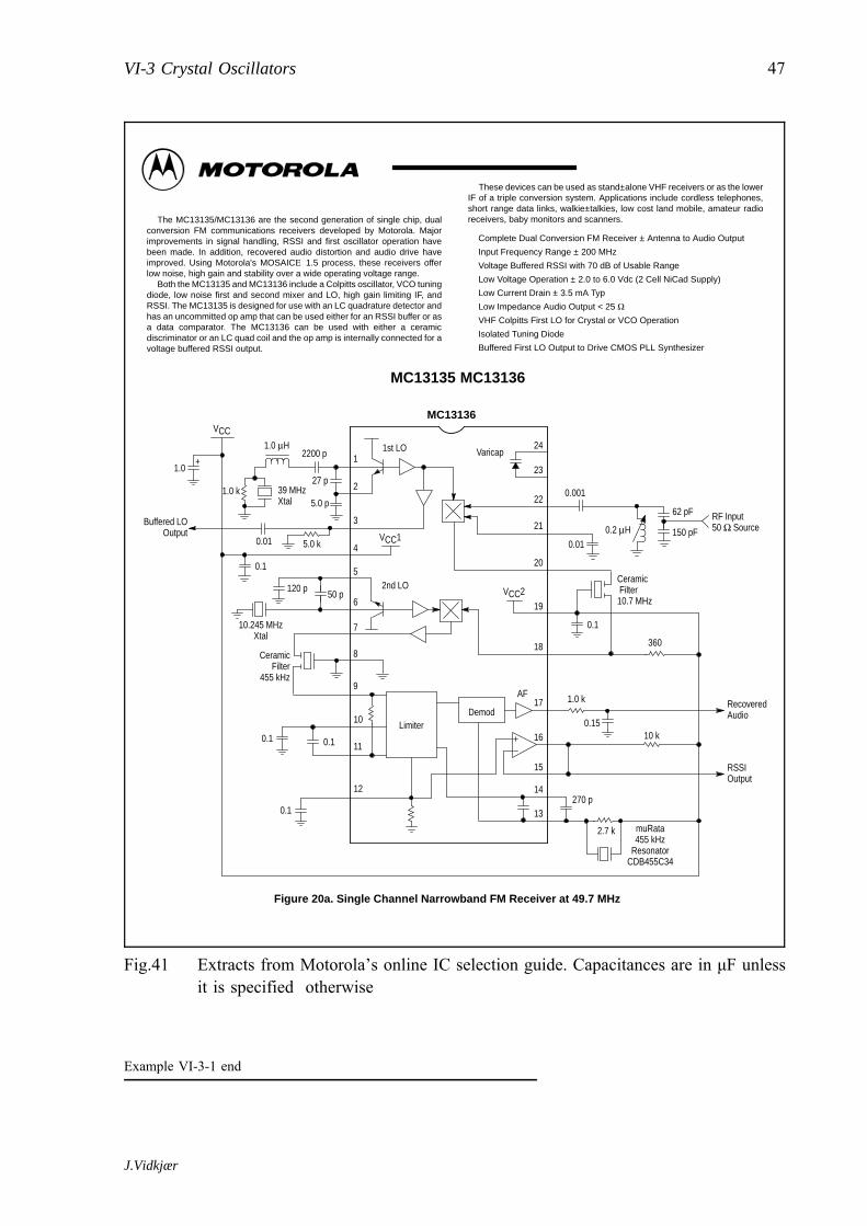
47VI-3 Crystal Oscillators
MC13135 MC13136
Figure 20a. Single Channel Narrowband FM Receiver at 49.7 MHz
24
0.2 μHRF Input50 Ω Source
62 pF
0.001
23
22
21
20
19
18
150 pF0.01
0.1
360
Ceramic Filter 10.7 MHz
muRata455 kHz
ResonatorCDB455C34
10 k
2.7 k
0.15
1.0 k17
16
15
14
13
12
0.1
2200 p
3
2
1
4
5
6
7
8
9
10
110.1 0.1
CeramicFilter
455 kHz
10.245 MHzXtal
39 MHzXtal
27 p
5.0 p
50 p
5.0 k
120 p
0.1
VCC
1.0
1.0 k
1.0 μH
AF
VCC22nd LO
VCC1
1st LO Varicap
LimiterDemod
Buffered LOOutput
RecoveredAudio
RSSI Output
0.01
270 p
MC13136Figure 20.
+
The MC13135/MC13136 are the second generation of single chip, dualconversion FM communications receivers developed by Motorola. Majorimprovements in signal handling, RSSI and first oscillator operation havebeen made. In addition, recovered audio distortion and audio drive haveimproved. Using Motorola's MOSAICΕ 1.5 process, these receivers offerlow noise, high gain and stability over a wide operating voltage range.
Both the MC13135 and MC13136 include a Colpitts oscillator, VCO tuningdiode, low noise first and second mixer and LO, high gain limiting IF, andRSSI. The MC13135 is designed for use with an LC quadrature detector andhas an uncommitted op amp that can be used either for an RSSI buffer or asa data comparator. The MC13136 can be used with either a ceramicdiscriminator or an LC quad coil and the op amp is internally connected for avoltage buffered RSSI output.
These devices can be used as stand±alone VHF receivers or as the lowerIF of a triple conversion system. Applications include cordless telephones,short range data links, walkie±talkies, low cost land mobile, amateur radioreceivers, baby monitors and scanners.
Complete Dual Conversion FM Receiver ± Antenna to Audio Output
Input Frequency Range ± 200 MHz
Voltage Buffered RSSI with 70 dB of Usable Range
Low Voltage Operation ± 2.0 to 6.0 Vdc (2 Cell NiCad Supply)
Low Current Drain ± 3.5 mA Typ
Low Impedance Audio Output < 25 ΩVHF Colpitts First LO for Crystal or VCO Operation
Isolated Tuning Diode
Buffered First LO Output to Drive CMOS PLL Synthesizer
Fig.41 Extracts from Motorola’s online IC selection guide. Capacitances are in μF unlessit is specified otherwise
Example VI-3-1 end
J.Vidkjær

48 Oscillators
J.Vidkjær
49
APPENDIX VI-A Oscillator Amplitude Stability
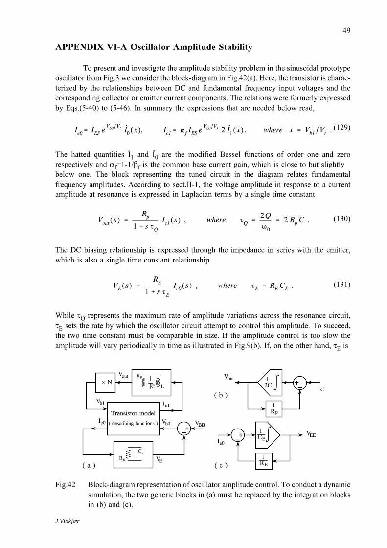
Fig.42 Block-diagram representation of oscillator amplitude control. To conduct a dynamicsimulation, the two generic blocks in (a) must be replaced by the integration blocksin (b) and (c).
To present and investigate the amplitude stability problem in the sinusoidal prototypeoscillator from Fig.3 we consider the block-diagram in Fig.42(a). Here, the transistor is charac-terized by the relationships between DC and fundamental frequency input voltages and thecorresponding collector or emitter current components. The relations were formerly expressedby Eqs.(5-40) to (5-46). In summary the expressions that are needed below read,
The hatted quantities Î1 and Î0 are the modified Bessel functions of order one and zero
(129)
respectively and αf=1-1/βf is the common base current gain, which is close to but slightlybelow one. The block representing the tuned circuit in the diagram relates fundamentalfrequency amplitudes. According to sect.II-1, the voltage amplitude in response to a currentamplitude at resonance is expressed in Laplacian terms by a single time constant
The DC biasing relationship is expressed through the impedance in series with the emitter,
(130)
which is also a single time constant relationship
While τQ represents the maximum rate of amplitude variations across the resonance circuit,
(131)
τE sets the rate by which the oscillator circuit attempt to control this amplitude. To succeed,the two time constant must be comparable in size. If the amplitude control is too slow theamplitude will vary periodically in time as illustrated in Fig.9(b). If, on the other hand, τE is
J.Vidkjær

50 Oscillators
too short the emitter decoupling becomes insufficient and the circuit may either start oscillat-ing with low amplitude at a wrong frequency or not start at all. As will be discussed below,a good design choice is to set the two time constants equal, like it was done to get the smoothamplitude start-up in Fig.9(a).
The time constant expressions in Eqs.(130),(131) are s-domain versions of the time-domain relationships that are shown in Fig.42(b) and (c), which are necessary to conductcalculations on how the oscillator amplitude evolves in time. With two integrators, theproblem to be solved is a second order differential equation. It is nonlinear due to thenonlinear relationships in the transistor description from Eq.(129) and no simple solutionexists. We shall, however, assume that such a solution with amplitude Vb1 has build up toformal stationarity where Barkhausen’s criterion applies,
If this solution is stable it is supposed that the oscillator amplitude remain stable when it is
(132)
disturbed by small perturbations δVb1. The question of amplitude stability is discussed fromthat point of view.
Linearizing around a given solution to find the current variation, which corresponds
Fig.43 Linearization of the block-scheme from Fig.42 and the corresponding signal flow-graph. Both describe how small amplitude variations develop in oscillations .
to an amplitude perturbation ΔIc1= GΔ11δVb1, may be represented by the block-scheme inFig.43. Here, linearized transconductances G11 through G00 depend on the actual large signalvoltages Vb1 and Vb0, and the block-scheme or the flow-graph provide directly
(133)
J.Vidkjær

51VI-A - Appendix - Oscillator Amplitude Stability
Introducing the determinant
a reorganization including collection of terms in equal powers in s gives
(134)
(135)
It is supposed that the response to an enforced amplitude pulse δVb1 should be stable andapproach zero if the underlying large-signal oscillation is stable. The last condition is fulfilledif the transfer function is stable, since in that case we have,
Stability requires that the poles of the transfer function are in the left half-plane only, a
(136)
condition that is met if all three coefficients in the second order denominator polynomial haveequal and - following the second order term - positive signs.
Fig.44 Linearized block-scheme and corresponding signal flow-graph for the oscillatoramplifier without the upper oscillation feedback loop that is present in Fig.43.
To illuminate the role of the constant term C in the denominator of Eq.(135), whichmust be positive, we consider small stationary perturbations of the driving signal in theoscillator amplifier if no feedback for oscillation was established. The corresponding block-scheme and signal flow-graph are given in Fig.44, from which we derive the transfer function,
J.Vidkjær

52 Oscillators
This ratio must be less than one in a self-limiting amplifier. It is the crossing slope of the
Fig.45 Stationary, large signal loop-gain response. Barkhausen’s criterion is met at the unitslope line.
(137)
stationary loop response curve at the stabilized amplitude, Vb1,osc, where the curve movesfrom the greater than one loop gain region to the smaller then one region as sketched inFig.45. The condition is expressed
The left hand side of this inequality is recognized as the constant denominator term. We have
(138)
seen that it is positive if the amplifier is adequate for oscillator applications.
Investigating the first order coefficient B in the s term of the denominator fromEq.(135), it is useful to introduce the time constant ratio
The condition to be fulfilled is written
(139)
a requirement that sets an upper bound on the time constant ratio
(140)
(141)
J.Vidkjær

53VI-A - Appendix - Oscillator Amplitude Stability
To be more specific in calculations, the partial derivatives of the current componentsand some of their interrelationships are required. From Eq.(129) we get directly
Comparisons between Eq.(142) and Eq.(5-95) show, that the effective fundamental frequency
(142)
transconductance in oscillations is related to G10 through,
Therefore, fulfillment of Barkhausen´s condition links derivatives and circuit components by
(143)
Using the modified Bessel function identities, [9] 9.6.27,
(144)
the complete set of partial derivatives is expressed
(145)
Finally, the determinant of large signal transconductances becomes
(146)
This quantity is positive for all positive arguments x.
(147)
J.Vidkjær

54 Oscillators
Positiveness of the determinant ΔG implies that the time constant condition inEq.(141) always will be met choosing Kτ=1 if the inequality in Eq.(138) applies. Then theunderlying requirement from Eq.(140) reads
Thus, setting the two time constants equal to each other gives a stable amplitude if the
(148)
amplifier is self-limiting so all polynomials coefficients in the denominator from Eq.(135) arepositive.
To gain more insight on circuit parameters, it is necessary to make the simplifyingassumption, that the amplifier is driven strongly in class C. The larger argument x, the smallerrelative difference between the modified Bessel functions, and we may estimate
One consequence of these assumptions is, that the determinant in of the derivatives looses
(149)
significance, so the denominator coefficient of Eq.(135) are approximated,
In the simplified version, the stability limit corresponding to Eq.(141) becomes
(150)
Substituting for the time constants from Eqs.(130),(131) sets directly a bound on the decouplig
(151)
capacitor CE in terms of the tuning capacitor C
so to keep the oscillator free of squegging, the decoupling capacitor must be carefully selected
(152)
and not just chosen from an "infinitely large" way of thinking.
Example VI-A-1 ( amplitude stability )
By this example we shall employ the self-limiting class-C amplifier design fromExample 5-3-1 in a 10 MHz prototype oscillator. Formerly the collector bias current wassupplied separately by a RF-choke, Lchk, but the tuning inductor may be used for that purposeas well, as it is done by the circuit in Fig.46. Summarizing previous results, the amplifier has
J.Vidkjær

55VI-A - Appendix - Oscillator Amplitude Stability
initial DC emitter current, transconductance, and voltage gain
Fig.46 10 MHz prototype oscillator based on the class-C amplifier from Example 5-3-1.Output waveforms were shown in Fig.9 for two settings of CE.
With maximum input signal, Vb1=125 mVrms, a gain reduction by a factor of three was
(153)
required and the DC current, the transconductance, and the voltage gain change to
To build an oscillator around this amplifier we must select the winding ratio of the
(154)
feedback transformer so that Barkhausen’s criterion is met. It gives
Using the results from Eqs.(5-95) and (5-100), the partial derivatives for the transistor current
(155)
components evaluate to
(156)
J.Vidkjær

56 Oscillators
(157)
Now the stability criterion from Eq.(141) gives an upper bound for stable time-constant ratios,
This limit can be verified by simulations on both the amplitude control block-scheme in Fig.42
(158)
Fig.47 Oscillator output for Kτ=10 showing the characteristic ’squegging’ waveform thathas named this type of instability.
or by complete circuit simulations based on the diagram in Fig.46. Examples of the latter typewere shown previously in Fig.9, where the lower, unstable case were a little above the limit,Kτ=4.5, in order to clearly demonstrate stationary oscillations. Deviating more severely fromthe stability limit gives unstable output waveshapes that in the audio frequency range soundslike the frogs squegging from which this type of instability was named. Fig.47 shows anexample where Kτ=10.
The time constants τQ was calculated in Example 5-3-1, and the maximum limitbecomes
(159)
J.Vidkjær

57VI-A - Appendix - Oscillator Amplitude Stability
This result should be compared to the maximum value from the simplified analysis,
As seen, we are on the safe side, but it is remarkable, that this simple solution to a complicat-
(160)
ed problem works. Going behind the result, it is observed that the correctly evaluated deriva-tives in Eq.(156) are in reasonable agreement with the simplifying assumptions from Eq.(150).
Example VI-A-1 end
Example VI-A-2 ( amplitude stability with current bias )
Current biasing is an ideal way to get the self-limiting amplification, which is
Fig.48 Simple feedback oscillator with current bias in common emitter configuration (a).Current biasing is often established by a current mirror (b).
necessary for stabilizing the oscillator amplitude. The basic amplifier properties was discussedearlier in section 5-3, and Fig.48 shows its inclusion in the transformer feed-back oscillatorthat was discussed in the previous example. The large signal control of amplitude is nowgoverned by the describing function block diagram in Fig.49, and its linearized counterpartis given by Fig.50. Compared to the similar schemes in the resistor biased case, Fig.42 andFig.43, we get the linearized current biased scheme below as the limit of RE approachinginfinity in Fig.43.
Since the amplitude stability analysis formerly was based on the linearization, stabilitycriteria for the present current biased oscillator are obtained from the resistor biased criteriaas the limit case of RE going to infinity. To do this, it is convenient to introduce a new timeconstant τEE. Instead of τE from Eq.(131) we use
J.Vidkjær

58 Oscillators
This time constant may be related to the current bias, since by Eqs.(5-99) and (142) we have
Fig.49 Block-diagram representation of oscillator amplitude control in a current biasedoscillator like Fig.48.
Fig.50 Linearization of the block-scheme from Fig.49 and the corresponding signal flow-graph.
(161)
In the limit of RE→∞, Eq.(135) reduces to
(162)
(163)
J.Vidkjær

59VI-A - Appendix - Oscillator Amplitude Stability
To ensure stability, the B coefficient in the denominator must still be positive, and now thecriterion reads
Under large drive conditions, where the approximations in Eq.(149) apply, we get the same
(164)
upper bound on the decoupling capacitor CE as we had before in Eq.(152), i.e.
(165)
Fig.51 Outputs from the oscillator circuit in Fig.48. The upper and lower curves are at thestable and unstable side of the stability criterion with Kτ=0.1675 and 0.1875 respec-tively.
To demonstrate the usefulness of the criteria for current bias we consider theoscillator circuit in Fig.48. It is organized to resemble the resistor biased oscillator fromExample VI-1-1 as close as possible, i.e. the normalized drive level xmax is maintained andthe current bias IEE is set equal to the former DC current from Eq.(154). Under such condi-tions the large signal transconductance Gm remains unchanged and Barkhausen’s condition isfulfilled to provide the same output voltage that we had before with unchanged load Rp andwinding ration N. Thereby, the stability bound becomes
J.Vidkjær

60 Oscillators
The two simulations below demonstrates the sharpness of the criterion by showing how the
(166)
oscillations build up with Kτ = .1675 and .1875 respectively. In the first case the amplitudeeventually stabilizes while in the second, spurious oscillations are sustained.
Example VI-A-2 end
J.Vidkjær

61VI Problems
Problems
P.VI-1
The oscillator in Fig.52 should be designed for maximum output at 2MHz without
Fig.52
transistor saturation, i.e. keeping Vce≥0. The supply voltage is VCC=6V, the loadresistor is RL=800Ω. The inductance at the primary side of the transformer isL=2.5μH and a Q-factor of QL=50. The amplifier should be designed to show a gainreduction of 1:2.5 when oscillations build-up from initial small-signal to the requiredamplitude. Assume that transistor βf is so high that the transistor input impedancemay be ignored and that the base emitter voltage is 0.6V.
- Calculate the bias current IET and the small-signal gain gmd.
- Find the transformation ratio N and capacitor C.
- Estimate the total harmonic distortion of the output voltage.
P.VI-2
Fig.53 shows a Colpitts oscillator circuit with a bipolar transistor. At the oscillatingfrequency, the transistor base and the collector supply are AC-grounded through thedecoupling capacitors Ccp1 and Ccp2. Ccp3 is a coupling capacitor and resistors Rb1,Rb2, and RE are bias resistors. Inductor Lrcf is a bias choke that may be consideredinfinitely large in design. The tuning components are CA, CB, and LC. They are allassumed lossless.
J.Vidkjær

62 Oscillators
The circuit should be designed to meet the following requirements,
Fig.53 Colpitts Oscillator Circuit
- frequency, f0 = 20 MHz,- output voltage Vo = 1.5 Vrms in RL= 200Ω,- loaded Q-factor, Ql > 25,- gain reduction at nominal output, Gm:gm ∼ 1:3.5
It is supposed that the transistor requires Vce > Vce,min=0.5V to prevent saturationeffects, that it has a forward current gain βf = 80, and that its base-emitter voltagein small-signal operation is 0.80V.
Calculate all component values of the circuit in Fig.53. Assume in the initial stepsof the design that the transistor is current biased and find the bias current IE. After-wards, RE should be chosen as high as possible to approximate the current biasconditions.
P.VI-3Consider a crystal operated in series resonance with resonance frequency f0. Showthat the frequency where the impedance becomes real differs from f0 by
if the electrode capacitance C0 is accounted for in details. Explain why the frequency
(167)
difference is insignificant.
P.VI-4
Fig.54 shows a Pierce crystal oscillator. It is supposed that the crystal is the 10 MHzcrystal from Eq.(111) with a series capacitance of Cser=22 pF. The crystal and theseries capacitor replaces the inductance LC in the oscillator design from ExampleVI-2-2 on page 29. All other components are kept unchanged.
J.Vidkjær

63VI Problems
Calculate the output voltage, the oscillator frequency, and the loaded Q-factor of the
Fig.54
oscillator in Fig.54.
P.VI-5
Fig.55 shows a Pierce crystal oscillator. It is supposed that the crystal is the 10 MHzcrystal from Eq.(111) used in series, impedance inverting mode like Fig.40(b) withinductance LC. The rest of the circuit is the oscillator design from Example VI-2-2on page 29, and all components values are kept unchanged from the example.
Calculate the output voltage, the oscillator frequency, and the loaded Q-factor of the
Fig.55
oscillator in Fig.55.
J.Vidkjær

64 Oscillators
J.Vidkjær

65
References and Further Reading
[1] N.M.Nguyen, R.G.Meyer,"Start-up and Frequency Stability in High-FrequencyOscillators", IEEE Journ.Solid-State Circuits, Vol.SC-27, pp.810-820, May 1992.Included in [2].
[2] B.Razavi,ed., Monolitic Phase-Locked Loops and Clock Recovery Circuits, Theoryand Design, IEEE Press 1996, Selection of 65 papers including approximately 10 onoscillator design and properties.
[3] R.S.Elliott, An Introduction to Guided Waves and Microwave Circuits, Prentice-Hall1993.
[4] G.Gonzalez, "Microwave Transistor Amplifiers" 2nd ed. Prentice-Hall 1997.
[5] D.B.Leeson, "A simple Model of Feedback Oscillator Noise Spectrum", Proc.IEEE,Vol.54,Feb.1966,pp.329-333. Included in [2].
[6] E.Hafner, "The Effect of Noise in Oscillators", Proc.IEEE, vol.54, pp.179-198,Feb.1966. Included in [2].
[7] A.van der Ziel, Noise in Solid State Devices and Circuits, Wiley 1986.
[8] M.E.Frerking, Crystal Oscillator Design and Temperature Compensation, Van-Nostrand 1978.
[9] M.Abromowitz,I.A.Stegun, Handbook of Mathematical Functions, Dover,NY, 1965
J.Vidkjær

66 Oscillators
J.Vidkjær
67
Index
Amplitude Noise . . . . . . . . . . . . . . . 13Antiresonance . . . . . . . . . . . . . . . . . 36Barkhausen’s criterion . . . . . . . . . . . 2Class C Amplifier
BJT oscillator example . 25, 29, 54,57
Colpitt’s Oscillator . . . . . . . . . . . . . . 18Crystal
antiresonance . . . . . . . . . . . . . 36equivalent circuits . . . . . . . . . . 35figure of merit M . . . . . . . . . . . 37parallel resonance . . . . . . . 36, 41poles and zeros . . . . . . . . . 36, 43series resonance . . . . . . . . . 36, 44
Crystal Oscillators . . . . . . . . . . . . . . 35Frequency Stability Factor . . . . . . . . 9Impedance Inversion . . . . . . . . . . . . 46LC Oscillators . . . . . . . . . . . . . . . . . 15Leeson’s oscillator noise model . . . . . 11Oscillators . . . . . . . . . . . . . . . . . . . . 1
amplitude stability . . . . . . . 10, 49Barkhausen’s criterion . . . . . . . 2crystal . . . . . . . . . . . . . . . . . . 35frequency stability . . . . . . . . . . 8LC couplings . . . . . . . . . . . . . 15negative conductance criterion . . 7noise . . . . . . . . . . . . . . . . . . . 11
Parallel Resonance . . . . . . . . . . 15, 35Phase Noise . . . . . . . . . . . . . . . . . . 13Pierce Oscillator . . . . . . . . . . . . . . . 18
LC tuned . . . . . . . . . . . . . . . . 29Seiler Oscillator . . . . . . . . . . . . . . . . 18
LC tuned . . . . . . . . . . . . . . . . 25Tank-Circuit . . . . . . . . . . . . . . . . . . 3
J.Vidkjær


