Characterisation and selective modification of semiconductor nanowires for electrical applications Dissertation zur Erlangung des akademischen Grades doctor rerum naturalium (Dr. rer. nat.) vorgelegt dem Rat der Physikalisch-Astronomischen Fakult¨ at der Friedrich-Schiller-Universit¨ at Jena von Diplom-Physiker Raphael Niepelt geboren am 3. M¨ arz 1982 in Hildesheim
Transcript
Characterisation and selective modification of
semiconductor nanowires for electrical applications
Dissertation
zur Erlangung des akademischen Grades
doctor rerum naturalium (Dr. rer. nat.)
vorgelegt dem Rat der Physikalisch-Astronomischen Fakultat derFriedrich-Schiller-Universitat Jena
von
Diplom-Physiker Raphael Niepeltgeboren am 3. Marz 1982 in Hildesheim
Gutachter
Prof. Dr. Carsten Ronning, FSU JenaProf. Dr. Marius Grundmann, Uni Leipzig
The prefix ”nano”, which is derived from νανoς, the ancient Greek word for dwarf, is
omnipresent in today’s technology. Nano stands for the use of nanoscale structured mate-
rials, which means that at least one dimension of the structure is in the nanometer range.
On this scale, the properties of the material are not only governed by the composition
but also the form and shape, which opens up a wide field of possible new applications.
Nano has become quite a trendy prefix, it is used to advertise a broad range of products,
from furniture polish to razor blades, from antifouling paint to functional clothing. Nano-
technology in the sense of science denotes the interdisciplinary research on processes and
objects on the nanoscale. The beginning of nanotechnology is often traced back to the
famous talk by Richard Feynman in 1959 ”There’s plenty of room at the bottom” [Fey60].
Today, we know that Feynman’s talk had hardly any influence on the development of the
modern nanotechnology [Tou05]. However, his visions on the possibilities that evolve due
to miniaturised devices on an atomic scale are still impressive.
The term nanotechnology was first used by Norio Taniguchi in 1974 to describe thin
film semiconductor techniques with thickness ranges in the order of a nanometer [T+74].
Finally, the invention of the scanning tunneling microscope by Binnig and Rohrer in 1981
[BR83] brought the possibility of imaging and manipulating single atoms. Other milestones
in the history of nanotechnology have been the discovery of the buckminster fullerenes
[KHO+85] and carbon nanotubes [I+91].
The electronic properties of nanoscaled materials can differ extremely from bulk due to
the increased surface-to-volume ratio of the nanostructures. The ongoing miniaturisation
of electronic devices down to pitch sizes of only 20 nm in 2012, that will be even reduced
by a factor of two by 2020 [ITR11], requires a deep understanding of the properties of
semiconductors at the nanoscale. Thus, nanotechnology and nanoelectronics have gained
major interest in the last decades. The integration of bottom-up synthesised nanostructures
into integrated circuits could contribute to cost reduction and material savings during
5
1 Introduction
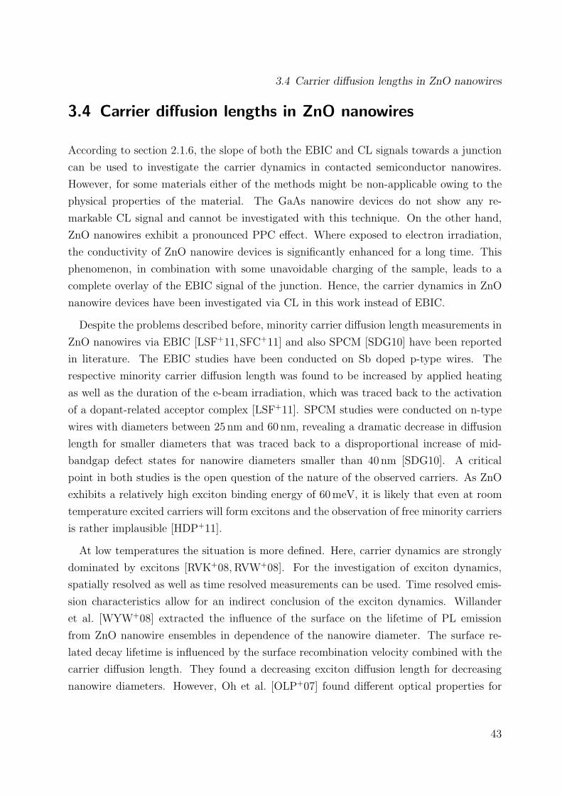
Figure 1.1: Publications per year on semiconductor nanowires determined with the ISI Webof Knowledge in January 2012 [isi12]. The used search term was semiconduct* AND
nanowir* and revealed a total of 7,296 results. The query might not include all publicationson this field, but the massively increased interest in semiconductor nanowires during thepast years is clearly visible.
fabrication. Furthermore, complex device structures in all three dimensions are imaginable
due to the integration of selectively arranged bottom-up nanostructures.
Quasi one-dimensional nanostructures, which are confined in two dimensions down to the
nanometer scale, are commonly named nanowires. The maximum diameter of a nanowire
is not clearly defined. Generally, the term is used for the description of wire-like structures
with diameters from one to a few hundred nanometers in diameter [LGY04,LL06,RBGN10].
The successful implementation of semiconductor nanowires into electric circuits roughly ten
years ago was categorised as a major breakthrough in science [Ser01,App02] and lead to
a massive boost on the research in such structures since then. The increased interest
in semiconductor nanowires can also be seen from the total number in publications on
semiconductor nanowires within the past 15 years, as displayed in Figure 1.1.
1.1 Semiconductor nanowires: Chances and challenges
Semiconductor nanowires are particularly distinguished by their unique transport proper-
ties governed by the extreme surface-to-volume and nanowire aspect ratio. They can be
easily grown up to length of micrometers and therefore be integrated into larger device
structures. On the other hand, the confinement in the other two dimensions leads to the
6
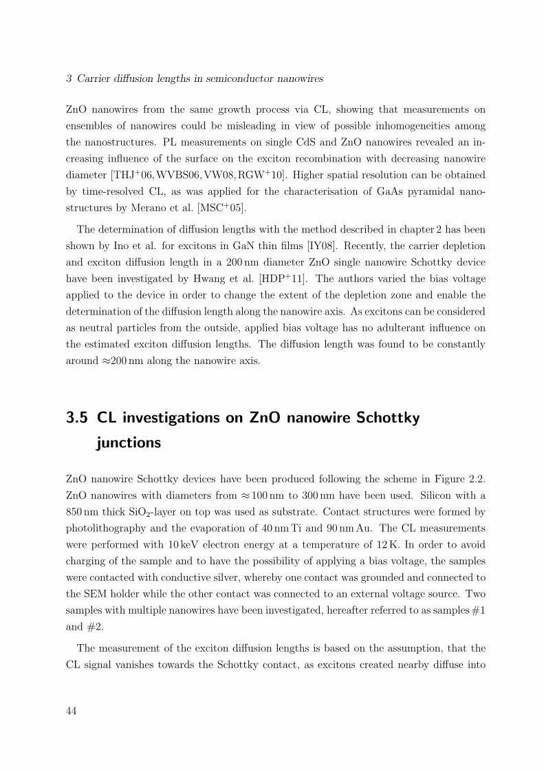
1.1 Semiconductor nanowires: Chances and challenges
formation of novel properties that can be used for applications. Nanowires with diameters
below the wavelength of light can act as photonic waveguides [VSM+07]. Furthermore, they
can even act as cavities for nanolasers [YYF10]. Electrically driven nanowire light emit-
ting diodes (LEDs) act as light sources that are smaller than the wavelength of the emitted
light [ZSR+08]. The small footprint of the nanowires reduces the lattice strain and allows
the combination of formerly incompatible materials via epitaxial growth [YYF10,WB11].
Thus, the integration of photonic materials like gallium nitride into a silicon based device
platform becomes imaginable despite large lattice mismatches.
Large-scale assembly methods have been developed for the integration of nanowires into
electrical circuits [WG09]. Moreover, advances in doping of semiconductor nanowires have
been made during the past few years [RBGN10,WB11]. New possibilities for the creation
of innovative memory devices with semiconductor nanowires are accompanied by new chal-
lenges regarding nanowire growth and assembly methods [LL07]. Due to the surface in-
fluence on the transport properties, nanowires are excellently adapted for the application
in sensing devices; optical [ZGH+09], chemical [CHC+08], and biological [CKJL10] sensors
have been demonstrated. Furthermore, nanowires can also be used as probes for single cell
endoscopy [LL07] or label-free DNA sensing [PTZL07].
Finally, the nanowire geometry provides potential advantages for energy production. Sili-
con nanowire solar cells [GBCM11] show a massive reduction in reflectance. Additionally,
nanowires arranged in periodic arrays provide excellent light trapping possibilities. Both
effects lead to improved absorption and a higher energy conversion efficiency. If the pn-
junction is placed along the nanowire surface, the active area, where charge separation
can take place, is multiplied compared to thin film devices. Thermoelectric applications
might benefit from the concurrence of high electrical conductivity and poor heat transfer
in semiconductor nanowires [LGY04]. With the use of piezoelectronic materials, nanowire-
based nanogenerators have been shown [Wan07].
Highly doped ZnO is often used in photovoltaics as a transparent conducting layer to
transport the carriers generated inside the active layer to the front electrodes of the solar
cell. ZnO nanowires have gained additional interest with the use as basic building blocks
in dye-sensitized solar cells (DSSC) [BA05,WCY+07]. In a DSSC the incoming light is
adsorbed by a dye attached to a wide bandgap semiconductor nanoparticle, originally
made of TiO2 [OG91]. The motivation of using nanowires instead of nanoparticles lies in
the provision of direct conduction paths for the electrons from the dye to the collecting
7
1 Introduction
electrode of the cell. With a band gap and electron affinity comparable to TiO2 [BA05]
ZnO nanowires are well-suited for the use in nanowire-based DSSC. In a similar approach,
ZnO nanowire solar cells have been realised by replacing the dye layer by extremely thin
absorber layers like CdSe [MB10]. Via functionalisation of the nanowire surface with
organic semiconducting layers it is possible to build organic/inorganic hybrid nanowire
solar cells [BHB+09]. All-oxide nanowire solar cells have been shown by covering ZnO
nanowires with p-type Cu2O nanoparticles [YY09]. Besides the field of photovoltaics, ZnO
nanowires have been applied to a huge variety of devices so far, including LEDs, nanolasers,
UV sensors, gas sensors, and nanogenerators [Wan09]. ZnO nanowires can be produced
cheaply and easily in a wide range of sizes and forms, adaptable to many different sample
geometries.
Due to the electronic properties of GaAs and the widespread use of this material in semi-
conductor industry, GaAs nanowires are promising candidates for future use in nanoscale
optoelectronic devices. LEDs [CSC+10] as well as Solar cells [MWK+11, TPKL11] have
both been presented based on GaAs nanowires. The application in photovoltaic devices
is encouraged by enhanced optical absorption [GPLN11]. The possibility of doping dur-
ing growth facilitates the synthesis of nanowire pn-diodes, either in radial [MWK+11] or
axial [RGL+10] geometry.
For the use of semiconductor nanowires in devices, it is essential to know and understand
the nature of the nanowires. Thus, advanced characterisation methods have to be developed
to investigate the electrical and optical properties of nanoscaled objects. Especially the
influence of the reduced size and the surface configuration on the nanostructure properties
has to be determined. Novel, functional elements for semiconductor devices can be achieved
by the selective modification of the nanowires, what can be done by either modifying the
wire composition or the surface conditions. Standard techniques used for the modification
of bulk material might not work in the case of nanowires, owing to the reduced size.
Therefore, altered or new techniques have to developed in order to selectively modify the
properties of semiconductor nanowires.
8
1.2 Goal of this thesis
1.2 Goal of this thesis
This thesis reports on different approaches to the characterisation and the modification of
the properties of semiconductor nanowires; in particular, the SEM based characterisation
of the transport properties of semiconductor nanowires, the manipulation of the optical
and electrical properties of ZnO nanowires by ion implantation and the funtionalisation of
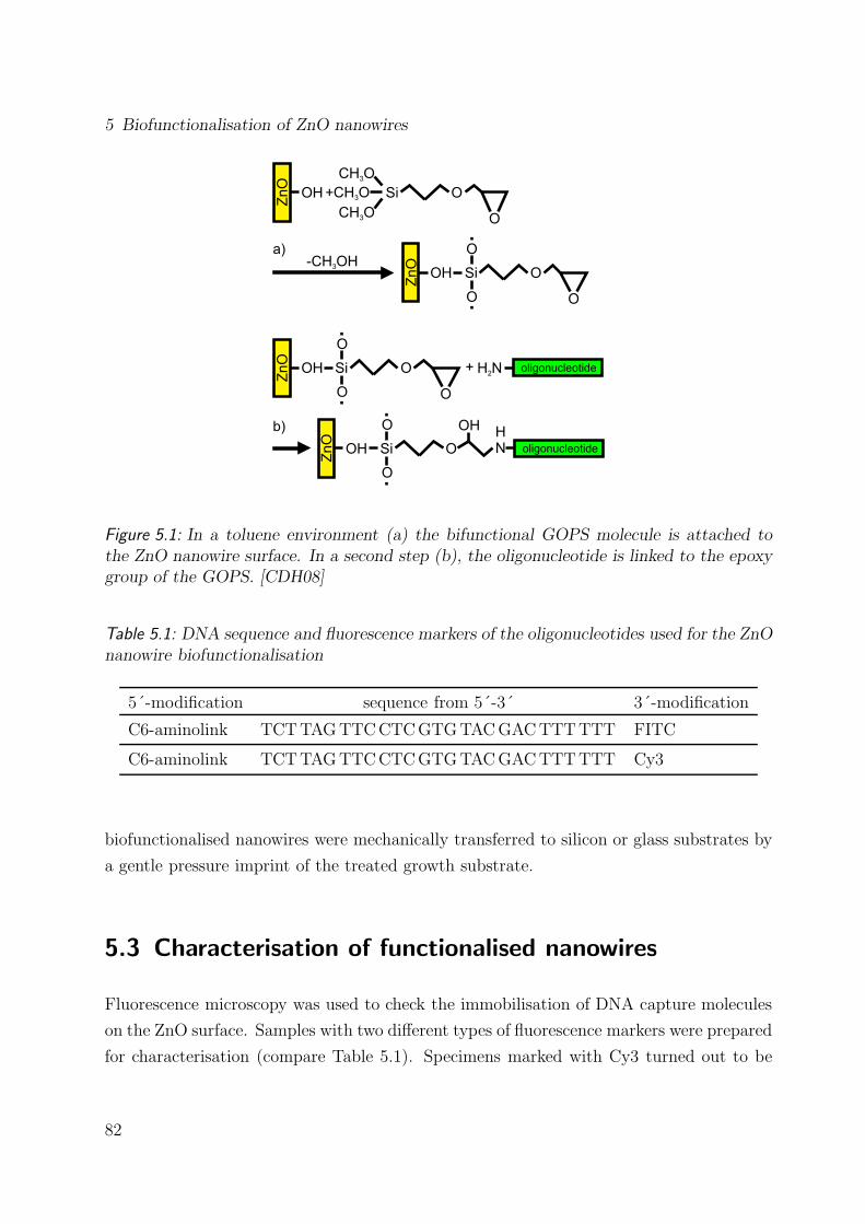
ZnO nanowires via DNA attachment.
Chapter 3 deals with the characterisation of semiconductor nanowires. On GaAs and
ZnO nanowire devices, measurements of the carrier diffusion length are conducted, which is
a key parameter for the application of nanowires in any electro-optical device. In the case
of GaAs nanowires, it is shown how surface passivation can enhance the carrier diffusion
length and thus improve the usability of the nanowires for device application.
The targeted manipulation of the nanowire properties helps to extend the field of possible
applications. Ion implantation, a standard doping technique in semiconductor industry,
can be used for enhancing the properties of semiconductor nanowires. Apart from doping,
ion implantation induced effects causing changes of the electrical properties of nanowire
devices are found. The unique interaction between ZnO nanowire devices and impinging
ions allows the detection of single ion impacts spatially confined to a small area of the
nanowire device. Ion implantation experiments on ZnO nanowires are conducted in order
to investigate these phenomena in chapter 4.
The surface has a large influence on the nanowire properties. Selectively modifying
the surface is another possibility for the targeted manipulation of nanowire properties for
the use in devices. An example of this is the biofunctionalisation of ZnO nanowires with
DNA. This treatment gives way to the development of a electrically driven, label-free DNA
sensing device. The biofunctionalisation of ZnO nanowires is investigated in chapter 5.
Detailed motivations for the individual approaches can be found at the beginnings of
the respective chapters.
9
1 Introduction
10
2 Background, simulations and
experimental details
2.1 Semiconductor nanowires
Semiconductors are defined as materials with a conductivity intermediate between insula-
tors and conductors, where the specific resistance of the material is in the range between
10−2Ωcm (GaAs, InAs) and 106Ωcm (selenium) [Inf04]. The electrical properties of a semi-
conductor can be modified by the systematic incorporation of impurities into the crystal,
called doping. This opened the door to the development of the variety of semiconductor
devices, including transistors, microchips, LEDs, and solar cells; components without our
modern world could not exist [Sch00]. The physics of semiconductors are well explained in
several textbooks [SN06,Ham10], that can provide further insight into the field of semicon-
ductor physics. Here, only some relevant terms addressed in this thesis will be discussed
very briefly.
In the scope this work, experiments have been conducted with semiconductor nanowires
made from GaAs and ZnO. Both materials belong to the group of compound semiconduc-
tors, where, further classified with respect to the main groups in the periodic system, GaAs
represents a III-V material and ZnO a II-VI material.
GaAs is a direct semiconductor with a bandgap of 1.42 eV at room temperature. It
is widely used for the application in optoelectronic devices like LEDs, laseres and solar
cells [BP07]. The material has some electronic properties, like the direct bandgap and
a higher electron mobility, which are superior to those of Si, especially for the use in
high speed microelectronics and photovoltaic devices. Thus, GaAs nanowires, that can be
synthesised in a bottom-up process from the vapour phase [GRB+09], have attracted great
research interest during the past few years.
11
2 Background, simulations and experimental details
ZnO is a direct wide bandgap semiconductor with a wide range of applications in several
fields of technology, including optics, optoelectronics, and biomedical sciences [OHM10].
The versatility of ZnO nanostructures and the avaibility of easy-to-handle nanostructure
synthesis methods have made ZnO one of the three most popular material systems in
the nano-material research [Wan09]. ZnO grows usually in a wurtzite crystal structure.
The high excitonic binding energy of 60meV entails potential for optoelectronic devices
using excitonic transitions. ZnO emits light in the ultraviolet range due to the bandgap
of ≈3.4 eV. Thus, ZnO has shown to be attractive for the development of light-emitting
devices in the ultraviolet region. Nanoscaled ZnO devices and their integration with the
mainstream semiconductor materials are of interest due to the large number of possible
geometries owing to the variety of available ZnO nanostructures [OHM10].
pn- and Schottky junction
The maximum of the available electron energy levels inside a solid at low temperatures is
called Fermi level. The Fermi level of an intrinsic semiconductor usually lies in the center
of the bandgap. Doping shifts the Fermi level upwards (n-type) or downwards (p-type).
On the junction between a p-type and a n-type region of semiconductor, free electrons
from the conduction band in the n-region will diffuse across the junction and combine with
holes. Filling a hole produces a negative ion on the p-side and leaves behind a positive ion
on the n-side. A space charge is induced, countervailing the diffusion process and leading
to an equilibrium state. The space charge creates a depletion region which inhibits any
further electron transfer over the junction unless an extra forward bias is applied. At the
pn-junction in equilibrium, the Fermi levels match on both sides of the junction, resulting
in a band bending in the energy band diagram.
An applied bias voltage will either drive the charge carriers towards the junction, re-
ducing the depletion zone and enabling current transport across the junction (forward
direction), or drive the carriers away from the junction, preventing any conduction (re-
verse direction). This rectifying diode behaviour of the p-n junction is the key element of
the enormous variety of solid-state electronic devices.
The junction between a semiconductor and a metal can also show rectifying behaviour.
Such a junction is called a Schottky diode. When the semiconductor and the metal form
an electrical contact, carriers from the semiconductor diffuse into energetically lower states
in the metal. Analogous to the pn-junction, a space charge region and a depletion zone
12
2.1 Semiconductor nanowires
Figure 2.1: Top view a) and side view b) scheme of a simple back-gate FET assembled on aSi-SiO2 substrate and contacted on both sides with Ti-Au metal contact pads. The carrierconcentration inside the nanowire channel and therefore the current between drain andsource contact can be adjusted by applying a voltage to the Si back gate.
build up in the semiconductor and cause a rectifying behaviour. Likewise existing metal-
semiconductor junctions without rectifying behaviour are referred to as ”ohmic”. Ohmic
contacts require a highly doped semiconductor in order to reduce the width of the depletion
layer to allow tunnelling and a uniform, extended contact area. Electrical contacts to
nanowires often show Schottky-behaviour due to the nature and limited size of the contact
region.
Semiconductor nanowire transistors
While methods for the large scale integration of nanowires into conventional integrated
circuits are still to be developed, field effect transistors (FETs) with nanowires as active
channels can be configured easily for research purposes [CZW+03, CFC+06]. A typical
setup is displayed in Figure 2.1. The nanowire is placed on an insulating substrate surface,
where source and drain contacts are defined to the nanowire ends. The substrate beneath
the insulating layer can be used as the gate electrode to control the current flow in the
nanowire channel. FETs manufactured in this simple construction type are usually referred
to as back gate FETs. In a more advanced setup, the gate electrode can also be placed on
top of the nanowire channel, separated by an insulating layer. This alternative design is
commonly termed top gate architecture [CL08].
Within this thesis, only nanowire devices contacted in back gate geometry have been
used.
13
2 Background, simulations and experimental details
Semiconductor detectors
In a semiconductor particle detector, the semiconductor material is used for the detection
of ionising radiation [SW09]. The principle is based on the detection of charge carriers that
are generated inside the semiconductor crystal by the incoming radiation and migrate to
the detector electrodes. The resulting current signal is then amplified and analysed, giving
access to the nature and/or energy of the detected radiation. The detector consists in
principle of a reverse-biased semiconductor pn-diode (see previous sections of this chapter).
The particle detection takes place inside the depletion layer of the diode junction. Electron-
hole pairs generated by the incoming radiation are separated by the internal electrical field
and a current pulse can be detected. The current signal is proportional to the energy
transferred to the electron-hole pair excitation process. Thus, it is possible to draw a
conclusion on the energy of the detected radiation particles from the current signal.
In order to build a detector with a wide energy detection range, a detector geometry
with an extended depletion zone that fully absorbs the incoming radiation is useful. For
this purpose often PIN (p-type-intrinsic-n-type) diodes are deployed. Here, an extended,
depleted, intrinsic region between a n-type and a p-type layer is used for the detection of
the incoming radiation. In order to achieve a reliable separation of the generated carriers,
PIN diodes have to be operated heavily biased, what is making high demands on the purity
of the used semiconductor material, as leakage currents have to be avoided. Commonly
used materials are high-purity silicon or germanium. Semiconductor detectors are widely
used in spectroscopy and in particle physics.
Nanowires could be used in principle as the active elements of nanosized particle de-
tectors. A high-energy particle detector based on an array of TiO–2 nanowires has been
developed by Angelucci et al. [ACC+06,ACD+06]. The nanowires act as nanosized, sep-
arated, and independent particle detectors and allow the spatially resolved detection of
incoming particels. Superconducting nanowires made from niobium or niobium nitride
can be used for the detection of single photons or other accelerated neutral particles
[SHH+09,ASC+09,MDS+09]. However, those detectors need low temperature (≈1-10K)
conditions to work. In chapter 4, the suitability of ZnO nanowires to be applied as ex-
tremely locally confined semiconductor detectors will be investigated.
14
2.1 Semiconductor nanowires
2.1.1 Synthesis of Semiconductor nanowires
Different wet-chemical or vapour phase deposition techniques can be used for the bottom-
up production of nanostructures and especially semiconductor nanowires [BDC02,Wan09].
Nanowires used for experiments in this thesis have been produced using the so-called
vapour-liquid-solid (VLS) process, first decribed by Wagner and Ellis in 1964 [WE64]. Here,
a metal seed particle, typically gold, is placed on the growth substrate. The substrate is
heated up beyond the melting point of the particle. Then, the particle is enriched with the
desired nanowire growth material from the vapour phase and forms an eutectic. Keeping up
the supply from the gas phase, the particle will finally be supersaturated and the supplied
material will begin to precipitate and recrystallise. In most cases, this happens at the
interface between the seed droplet and the substrate. The process will continue as long as
material from the vapour phase is provided. The material precipitated from the eutectic
lifts up the droplet, forming the nanowire. The nanowire diameter is governed by the
diameter of the seed droplet.
Although the VLS model has to be expanded to be capable of explaining the growth
of compound semiconductor wires [BMS+06], it is widely adopted as a standard growth
model for vapour phase deposition techniques of semiconductor nanowires. Recently, there
have been some attempts to further generalise and expand the model [Moh08,WDJ+09].
Zinc oxide nanowires used in this work have been synthesised in a horizontal tube furnace
following [BMS+06]. A thin Au layer of ≈5 nm thickness was applied to the substrates
prior to the growth process. As source material, 2 g high-purity ZnO powder was placed
in the middle of the furnace and heated up to 1350 C in order to evaporate the material.
The growth substrates were placed somewhat towards the end of the furnace where a
temperature between 1100 C and 900 is present, causing the Au layer to melt and form
nanowire seed droplets. The growth pressure was between 15 and 150mbar. A gas flow
of 50 sccm argon was used to transport the ZnO vapour to the growth substrates. Typical
growth times for the synthesis of nanowires with some tens of µm are between 15 and
30min.
Gallium arsenide nanowires were synthesised at the University of Duisburg with a com-
reactor [GRB+09,GLR+10,RGL+10]. Polydisperse metal seeds were formed by evapora-
tion and subsequent annealing of a thin Au layer of nominally 2.5 nm thickness, resulting in
seed particles with diameters from 80 nm to some 100 nm. Trimethylgallium (TMGa) and
15
2 Background, simulations and experimental details
Tertiarybutylarsine (TBAs) were used as group-III and group-V precursors. The wires were
doped during growth in order to receive axial pn-junctions by applying Diethylzinc (DEZn)
or Tetraethyltin (TESn) as dopant precursors for the p-type (lower) and n-type (upper) part
of the nanowire. The doping procedure led to carrier concentrations of NA = 1.6 ·1019 cm−3
in the lower, and ND = 1 · 1018 cm−3 in the upper nanowire part [RGL+10].
2.1.2 Contacting of semiconductor nanowires
Electrical contacts have to be applied to the nanowires in order to conduct electrical mea-
surements on them. ZnO nanowires were contacted at the IFK in Jena via photolithogra-
phy, a well known and widely used method to prepare electrical contacts on a micrometer
scale. Hereby, an UV-sensitive photoresist is exposed to light through a microstructured
mask and developed afterwards. The remaining resist has adopted the masks structure and
can be used as a mask itself for the evaporation of metallic contacts. The minimum feature
size available depends on the light wavelength used for exposure as well as the performance
of the lithography apparatus. The resolution limit of the system used in this thesis is about
1-2 µm, where fully developed structures smaller than 5 µm are very difficult to achieve.
Thus, nanowires that are to be contacted via photolithography should feature a minimum
length of a few µm, which however can be attained easily in the VLS process.
The sequence of work steps used for the contacting of ZnO nanowires is outlined in
Figure 2.2. First, the nanowires are transferred from the growth substrate to a clean SiO2-
Si substrate via contact imprint. One is capable of adjusting the density of nanowires
dispersed on the substrate by varying the force applied during the imprint. Directional
sliding of the growth substrate further helps to align the nanowires with a specific orien-
tation [FHJ+08]. Second, the later contact structures are predefined via photolithography
using the negative photoresist TI 35ES from Michrochemicals [mic12]. In this work, a
lithography mask with 15 pairs of contact pads with a 5 µm wide gap between the coun-
terparting pads was used. The underlying nanowires were hit just by chance, depending
on the density of the dispersed nanowires on the substrate. Third, Ti and Au were evap-
orated onto the pre-patterned sample. After the lift-off of the developed resist, only the
predefined contact structures and the imprinted nanowires remain. Fourth, the sample is
fixed on a chip carrier and the contacts are bonded to the carrier pins enabling electrical
measurements in the lab environment. An SEM image of contacted nanowires between the
evaporated contact pads is shown in Figure 2.2 e).
16
2.1 Semiconductor nanowires
Figure 2.2: Nanowire contacting sequence used for ZnO nanowires throughout this thesis:a) Nanowire transfer by imprint. b) Contact contour predefinition by photolithography.c) After evaporation of Ti/Au and lift-off, predefined contact structures remain. d) Bondingfor electrical connection of FET terminals. e) SEM image of contacted nanowires.
The contact composition of Ti and Au was chosen in order to get both durable and
conductive contacts. Ti is known to act as an adhesive agent, countervailing undesired
contact cracking or peeling during the bonding process [Uen92,JXW10]. The Ti-Au system
has been reported to form ohmic contacts on ZnO nanowires [YNPR05]. However, the
same material system was found to form Schottky contacts in other studies [ITY+06]. In
an overview study on the electrical properties of ZnO nanowires Schlenker et al. [SBW+08]
point out that the transport properties of ZnO nanowires can be influenced by so many
factors that a reliable transfer of results from one lab to another is quite impossible. Thus,
optimisation of the evaporated contacts, e.g. by replacing Ti-Au with a more complex
system like Ti-Al-Pt-Au [ITY+06], has played a less important role in the scope of this
work, as the experimental conditions in the lab do not meet the high demands that are
necessary to come to a reliable statement in this field.
The contacted ZnO nanowires usually showed s-shaped IV-characteristics that imply
a Schottky contact on both sides of the nanowire. However, as the contacting is done
by a random success process, the Schottky barriers on both sides of the nanowire might
differ significantly in height and therefore the IV-characteristics often remain asymmetric.
Multi-wire devices are typically found to provide more symmetric characteristics, as their
curves represent an average of the characteristics of several wires. By applying a voltage
17
2 Background, simulations and experimental details
to the silicon substrate, the device can be used as a simple FET. Hereby, the nanowire
represents the transistor channel between the source and the drain contact. The substrate
below the oxide layer serves as back gate electrode.
In order to produce single nanowire transistors, it is possible to cut unwanted bridging
wires between the contact pads with a focused ion beam (FIB) system. By cutting all
but one nanowires, a single nanowire device can be produced easily by this rather simple
contacting approach.
The contacting of GaAs nanowires investigated in this work was carried out with electron
beam lithography at the University of Duisburg-Essen. The process is described in detail
in [GLR+11]. Ohmic contacts on the p-doped nanowire part were formed by evaporation
of Pt (5 nm)/Ti (10 nm)/Pt (100 nm)/Au (300 nm), and subsequent rapid thermal annealing
for 30 s at 360 °C, while Pd (50 nm)/Ge (170 nm)/Au (80 nm) contacts followed by annealing
for 30 s at 280 °C were used for the n-doped part.
2.1.3 Electrical characterisation
Electrical characterisation of nanowire devices within this work was conducted in an EP6
probe station by Suss MicroTec [sus12]. The probe station can be darkened to avoid photo
induced side effects on the measurement. A Keithley 237 [kei12] source measurement unit
(SMU) was used for current-voltage measurements. The SMU allows accurate current
measurements down to ≈1 pA and is optimised for current measurements at a set bias
voltage. A custom LabView™ software written by Steffen Milz [Mil10] allows computerised
electrical measurements. Current-voltage (IV) as well as transfer characteristics of the
devices can be measured.
The transfer characteristic of a FET describes the current flow between the source and
the drain electrode at constant bias while the voltage applied to the gate electrode is
varied [SN06]. Thus, it is describing the switching and amplification behaviour of the
transistor. From the transfer characteristic, it is possible to determine the type of dopant
of the semiconductor material in the channel and the working mode of the transistor.
Depletion mode transistors provide a conductive channel that can be depleted when a gate
voltage is applied. On the contrary, enhancement mode transistors own a usually depleted
channel that can be populated by an applied gate voltage.
18
2.1 Semiconductor nanowires
2.1.4 Persistant photoconductivity
ZnO devices, especially thin films and nanodevices, often show persistent photoconduc-
tivity (PPC), which denotes a photo induced excess conductivity with a rather slow drop
in conductivity after stopping the excitation [WLS+11]. In a semiconductor, illumination
with light of an energy higher than the bandgap leads to charge carrier generation due
to the excitation of electron-hole pairs. Thus, semiconductors always show an enhanced
photoconductivity. However, the time scale for the recombination of photoinduced charge
carriers lies usually in the region below one second. For ZnO nanowires, recombination
times as short as 100 ps have been estimated [RGW+10]. However, much longer times-
pans on the order of minutes have been observed for the conductivity to drop down to
pre-illumination level due to PPC [PHRJD+08,WLS+11,BSS+11].
Investigations on the PPC of coated and uncoated ZnO nanowires in different atmo-
spheres point to a surface related effect [PHRJD+08, SHL+09]. In [PHRJD+08], Prades
et al. attribute the PPC to the separation of the photogenerated carriers due to a sur-
face built-in potential. Owing to band-bending towards the surface, generated holes will
accumulate near the surface, while the electrons remain in the middle of the nanowire,
causing the increased conductivity. The delayed decline towards the initial value after
terminating the illumination is attributed to a comparably slow oxygen-assisted surface
recombination mechanism. Here, oxygen adsorbed on the surface traps electrons from the
nanowire conduction band. Those electrons are able to recombine with the holes accumu-
lated near the surface, whereupon the oxygen molecule is desorbed. In principle, photo
induced desorption of oxygen from the nanowires should be observable, as was reported
from ZnO bulk [CFS74]. There have not been any reports on the desorption of oxygen from
ZnO nanowires under illumination so far. The model described above could also work with
oxygen-containing molecules like water or CO2, where the desorption of the latter indeed
has been reported [BSS+11].
Some ideas exist to take advantage of the PPC for the development of non-volatile
memory or optical switches and integrators [WCLK11]. A negative consequence of this
phenomenon is the need of a reset process in order to do reproducible measurements.
This issue becomes important for the application of such structures as sensing elements
or switches. Some possible reset processes have already been investigated. Prades et al.
reported a faster conductivity drop for an increased current flow through the wire, caused
by thermally enhanced recombination of the separated carriers [PHRJD+08]. White et al.
19
2 Background, simulations and experimental details
applied a high gate voltage pulse to ZnO FETs in order to reset the devices [WCLK11].
Wang et al. achieved a significantly shortened decay time of the PPC by illuminating the
nanowires with a 980 nm infrared laser [WLS+11]. ZnO nanowire devices should always
be measured very carefully and just under defined lighting environment if no well defined
reset process is available.
2.1.5 Electron beam induced current measurement
The analysis of the electron beam induced current (EBIC) within a SEM is a powerful tool
for the characterisation of semiconductor samples, enabling the determination of material
properties like carrier lifetime, diffusion length, defect energy levels and surface recombina-
tion velocities [PBPR07,Lea82]. In early experiments, this technique was mostly used to
visualize sites of enhanced recombination, like dislocations or stacking faults, inside semi-
conductor crystals [WK64,Hol74]. However, by scanning the beam in a direction normal
to the plane of a pn-junction, the decrease of the current with increasing distance from
the junction permits the determination of the minority carrier diffusion length, as already
described in 1965 by Higuchi et al. [HT65].
Working principle
In this work EBIC was used to investigate axial pn-junctions in GaAs semiconductor
nanowires with the focus on the investigation of the minority carrier diffusion length. The
working principle of such an EBIC measurement is displayed in Figure 2.3 a). An electron
hitting a semiconductor sample like the nanowire in the figure will dissipate its kinetic
energy through the sample and therefore generate charge carriers at its impact point. If
those charge carriers reach a pn-junction, they will be separated and can be detected by
an external current measurement setup. The majority carriers will be repelled at the
internal electrical potential, as displayed in Figure 2.3 b). Only the minority carriers
will contribute to the current signal. If the electron beam is moved off the junction, the
induced minority carriers will only be detected if they are able to diffuse to the space charge
region of the junction, where the internal electrical field is present. Measuring the induced
current with respect to the electron beam position allows the determination of the diffusion
characteristics of the respective minority carriers. The method does not necessarily require
an axial pn-junction; any region with an internal electrical field can be used to separate
20
2.1 Semiconductor nanowires
Figure 2.3: EBIC working principle: a) EBIC measurement setup scheme. b) During themeasurement, both majority and minority carriers can diffuse to the junction. Only therespective minority carriers are collected, whereas the majority carriers of both sides arerepulsed. c) From the EBIC signal along the wire axis, minority carrier diffusion lengthsof both p-type and n-type region can be extracted.
the induced carriers. An example of the EBIC based determination of the minority carrier
diffusion length on a silicon-nanowire-gold Schottky contact can be found in [AHP+08].
Minority carrier diffusion length
The minority carrier diffusion lengths can be extracted by analysing the reduction of the
EBIC signal, recorded along the axis of the nanowire away from the junction. The signal
strength is given as
I = I0 · e−x
L (2.1)
21
2 Background, simulations and experimental details
where I0 is the intensity at the edge of the junction, x is the distance from the junction
and Lp and Ln are the minority carrier diffusion lengths for holes and electrons following
Li =√
Di · τi (2.2)
with Di and τi as the respective diffusion coefficient and carrier recombination lifetime. It
is important that the device is investigated under low injection conditions (LIC), which
means that the amount of excess carriers excited in the sample has to be small compared
to the doping level [CC94]. If LIC does not apply, one might measure a diffusion length of
both minority and excess carriers. The injection conditions can be checked with computer
simulations and will be discussed in more detail in a following paragraph. Scanning a
nanowire with an axial pn-junction allows the extraction of both electron and hole diffusion
lengths on the respective p- and n-type site of the junction simultaneously, as shown in
Figure 2.3 c). Very similar to such an experiment, the minority carrier diffusion length
can also be determined by photocurrent measurements within a micro-photoluminescence
(µ-PL) setup. However, the use of an electron beam results in a far better spatial resolution.
Surface recombination velocity
It is possible to extract the surface recombination velocities from the relation of the mea-
sured minority carrier diffusion lengths of nanowires of different diameters. The diameter of
our samples is way below the bulk diffusion lengths [Hwa69,WOPS81]. Thus, a determined
value Li has to be interpreted as an effective diffusion length
L∗
i =√
Di · τ ∗i (2.3)
with an effective lifetime τ ∗i that is governed by the surface recombination velocity S of
the nanowires [AHP+08]. This parameter τ ∗i is connected with the surface recombination
velocity S and the bulk lifetime τb via
1
τ ∗i=
1
τb+
4S
d(2.4)
22
2.1 Semiconductor nanowires
where d denotes the nanowire diameter [DST+11]. This relation is only valid to certain
values of S, as it is based on an approximation. The exact relation between τ ∗i and τb
resulting from the continuity equation of the carrier concentration profile is
1
τ ∗i=
1
τb+
4β2D
d2(2.5)
where D is the diffusion constant, d is the nanowire diameter and β is defined by
βJ1(β)− ΛJ0(β) = 0 (2.6)
where Λ is
Λ =d · S2D
(2.7)
with J1 and J0 as the 1st and 0th order of Bessel function of the first kind. If Λ < 1, the
approximation β =√2Λ leads to an error in β of less than 10% [DST+11]. This leads to
an upper limit for S for the validity of the approximation. The limit for a 300 nm diameter
GaAs nanowire with an electron diffusion coefficient of 200 cm2/s in the p-type region [JG89]
can be estimated to:
d · S2D
≤ 1 =⇒ S ≤2D
d=
2 · 200 cm2/s
300 nm= 1, 33 · 107 cm/s (2.8)
For the holes in the n-type region the respective upper limit can be estimated using
values from the same reference to S ≤ 6 · 105 cm/s. For both holes and electrons in our
nanowires S is below the upper limit and therefore the error caused by the approximation
is less than 10%.
Using the relations between L, τ , and S enables one to extract the surface recombination
velocity from the diameter dependence of the observed minority carrier diffusion lengths.
Injection conditions
As mentioned above, a conclusive determination of Li is only feasible when the measure-
ment is carried out in the so-called low injection regime [CC94]. Within LIC, the resulting
values of Li and τi are independent of the amount of excess carriers produced in the sample
∆p. LIC is only fullfilled when ∆p is comparatively small in reference to the doping level.
To verify this, one has to determine ∆p and compare it to the doping level. The value of
23
2 Background, simulations and experimental details
∆p can be analytically derived for bulk material by comparing the activation volume and
the deposited energy E0. In the case of nanostructures the distribution of energy inside
the sample is strongly dependant on the sample structure and dimension. Therefore, the
Monte Carlo code Casino v3.2 [DPDC+11] was used to determine the energy distribution
inside an irradiated GaAs nanowire lying on a SiN substrate. With E0 distributed inside a
volume V , it is possible to calculate the excess carrier generation rate G0 following [Kle68]
G0 ≈E0
3Eg·1
V(2.9)
expressing the amount of carriers excited per volume by a single electron. The energy
distribution E0/V provided by the Monte Carlo code depends on the choice of spatial
resolution during the simulation. Here, the simulation was conducted for volume cells
of 4 · 4 · 4 nm3 size. Larger simulation cell sizes would lead to a more uniform energy
distribution. However, if the cell size is not small enough compared to the carrier diffusion
length, the distribution will be smeared out too much and a reasonable conclusion on the
injection regime following G0 is not possible. For a certain electron beam current IB and
a known excess carrier lifetime τexc the value of ∆p can be estimated with
∆p ≈G0
eIBτexc (2.10)
where e is the elementary charge. Within GaAs bulk samples, the existence of LIC is often
very unlikely due to the relatively high excess carrier lifetime and the µm-ranging of the
carrier diffusion lengths [CC94]. However, within GaAs nanowires, excess carrier lifetimes
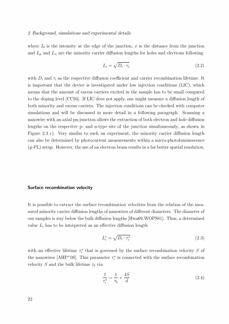
and diffusion lengths are strongly reduced due to surface influence. In Figure 2.4, ∆p is
displayed for a nanowire with 200 nm diameter and typical electron current density (40 pA)
and acceleration voltage (10 kV) values used in this thesis. With the carrier lifetimes
estimated for the minority carriers from the EBIC profiles, ∆p is always more than one
order of magnitude below the typical doping level.
The EBIC measurements in chapter 3 have been conducted with a JEOL JSM-6490
scanning electron microscope equipped with a LaB6 cathode and a Gatan SmartEBIC
analysing system. The electron beam current used was always below 40 pA, ensuring low
injection conditions at 10 kV accelerating voltage.
24
2.1 Semiconductor nanowires
Figure 2.4: Distribution of ∆p in a nanowire with 200 nm diameter for an electron currentof 40 pA and acceleration voltage of 10 kV determined using Casino v3.2 and the carrierlifetimes estimated for the minority carriers from the EBIC profiles. The concentrationof excess carriers ∆p is always more than one order of magnitude below the doping level,which is 1.6 · 1019cm−3 in the nanowire p-type region (left side) and 1 · 1018cm−3 in then-type region (right side).
2.1.6 Cathodoluminescence
Cathodoluminescence (CL) denotes the phenomenon of light emission from a semiconductor
impinged by an energetic electron beam [MG74], caused by radiative recombination of the
excited charge carriers. The observation of such luminescence inside a cathode ray tube
led originally to the discovery of ”cathode rays” or electrons. CL emission characteristics
give access to the electronic properties of the investigated semiconductor material. If
applied within a SEM, CL allows the investigation of luminescence properties and therefore
recombination dynamics of a sample with spatial resolution [YH86,PR07].
Electron-hole pairs generated inside a sample by an incoming electron beam can re-
combine either radiatively or non-radiatively. The probability of the one or the other
case to happen depends on the local environment of the charge carriers. Therefore,
CL measurements offer access to the local carrier dynamics of selected nanostructures,
gaining information of the influence of the shape of the nanostructures on the carrier
transport and recombination mechanisms. Non-radiative recombination is often induced
by defects in the semiconductor crystal. Thus, CL can give information on the crystal
quality of a nanoobject [PPAD06]. As an example, information about the uniformity
of the optical and electrical properties of bottom-up grown ZnO nanowires can be ob-
25
2 Background, simulations and experimental details
Figure 2.5: CL working principle. The electron beam induced luminescence is colimated bya parabolic mirror and coupled into an optical spectroscopy system. With the monochro-mator, the incoming light can be spectrally decomposed and analysed as a function ofwavelength. A photomultiplier or a CCD camera can be used for signal detection.
tained [NKR+04, PYE+07,CAM+11]. Furthermore, CL can be used for studying carrier
dynamics in single quantum dot devices [MSC+05].
In the presence of an internal electrical field, generated electron-hole pairs must not
necessarily recombine but might get separated before the recombination takes place. De-
tecting such separated carriers is the principle of the EBIC measurement explained in
section 2.1.5. However, it is also possible to measure the electron beam induced CL sig-
nal instead of the induced current to obtain information on the diffusion dynamics of the
excited carriers. While with EBIC the separated carriers are monitored, CL counts the
non-separated, radiatively recombining carriers. In addition, also non-radiative recombi-
nation dynamics can be monitored in principle when it is possible to measure the EBIC
and CL signal simultaneously on the same sample [Hol89].
The working scheme of the CL setup used in this work is displayed in Figure 2.5. A
parabolic mirror is used to collimate the emitted luminescence and couple the light into
a chamber-mounted monochromator with attached optical sensors, enabling spectroscopic
analysis of the CL emission. The signal is detected by either a CCD or a photomultiplier
attached to the monochromator exit slit. Besides the monochromatic imaging, it is also
possible to drive the machine in panchromatic mode and detect the overall light emission
independent of the wavelength of the emitted light. Regardless of the working mode, the
CL setup always collects the emission of the whole sample, caused by a local excitation
26
2.1 Semiconductor nanowires
from the confined electron beam. Thus, the excitation is spatially resolved, and not the
CL signal.
Analogous to the EBIC technique, CL measurements can be used for the extraction of
carrier diffusion lengths by monitoring the decay of the signal towards a pn- or Schottky
junction. In chapter 3, CL was used in this manner to determine the carrier diffusion
dynamics inside ZnO nanowires. According to equation 2.1 in the previous section, the
probability that electron beam induced carriers will be separated in the internal field of the
junction and contribute to EBIC drops exponentially with increasing distance between the
position of carrier generation and the junction. In the same way, it becomes more likely
for the carriers to recombine with their counterparts. Therefore, in the case of a negligible
or constant ratio of non-radiative to radiative recombination, the CL intensity towards the
junction will decrease by [IY08]
ICL ∝ A · (1− e−
x
LD ) (2.11)
where ICL is the CL intensity, x is the distance from the junction and LD is the carrier
diffusion length. Thus, the carrier diffusion lenght can be extracted by measuring the CL
intensity along the nanowire, as shown in Figure 2.6 a) and b). The fit of equation 2.11 to
the intensity characteristics directly gives the diffusion length of the recombining carriers,
which is in this case (ZnO nanowire) the exciton diffusion length.
The CL measurements in chapter 3 have been conducted with a Gatan MonoCL3 system
on a JEOL JSM-6490 scanning electron microscope with a LaB6 cathode. The system is
equipped with a helium cooling stage for temperatures between 6K and 300K. Further
details on the CL system can be found in [Bul09].
The electron beam current used was always about 100 pA. The applied acceleration
voltage was 10 kV. In parallel to section 2.1.5, Casino simulations give the number of
electron beam induced excess carriers ∆p. Under the applied conditions, ∆p is always
lower than 1 · 1012 cm−3 and thus more than one order of magnitude below the doping
level of intrinsic ZnO which is in the range of 1017 cm−3 [GSLY05], ensuring low injection
conditions. All diffusion length measurements have been performed at 12K temperature.
27
2 Background, simulations and experimental details
Figure 2.6: Example for the estimation of the exciton diffusion length in ZnO via CL. In a),the CL image of a ZnO nanowire contacted by an Au-Ti contact pad is shown. Only theuncovered part of the nanowire is exhibiting a significant luminescence signal. The insetshows the SEM image from the white dotted rectangular area. In b), that CL intensityalong the dashed cyan line in a) is plotted. The exponential fit of the intensity drop alongthe nanowire towards the contact region allows the determination of the exciton diffusionlength.
2.1.7 Photoluminescence
Photoluminescence (PL) denotes the light emission from a semiconductor excited by ab-
sorbed photons. In principle, PL and CL are relying on the same mechanisms, distinguished
just by the nature of the excitation. An advantage of PL over CL is avoiding carbon de-
position on the surface of the investigated sample, a phenomenon that is often observed
inside a SEM, which makes PL the favoured method for the investigation of surface related
effetcts. Additionally, the PL intensity depends on the excitation wavelength, a detail that
can provide further information on the excitation mechanisms in the sample [YH86]. It is
also possible to visualise the depletion zone in electrical devices [HZAL07]. PL spectra in
the scope of this work have been recorded by Apurba Dev, University of Bremen. Details
on the setup can be found in [Ric10]. The Photoluminescence (PL) measurements were
carried out in a liquid-helium-cooled cryostat at 10 K. A He–Cd laser was used for excita-
tion at a wavelength of 325 nm. The emission signal was detected either with an Ocean
Optics HR4000 spectrometer or a Jobin Yvon HR320 monochromator with an attached
CCD camera.
28
2.2 Ion-solid interactions
2.2 Ion-solid interactions
The irradiation of material with energetic ions is the basis for a variety of methods for
the analysis and processing of materials. An ion that is impinging on a solid material will
be slowed down by flying through the surrounding matter and transferring its energy to
the local environment. The energy dissipated inside the target can result in the breakup
of existing crystal structures, rearrangement of the target atoms and the creation of voids
inside the target material. By selectively controlling these effects, ion beam irradiation can
be applied to the processing of materials. On the other hand, the same effects have to be
considered for ion implantation processes, where the ion beam is used to implant a distinct
amount of atom species into a target material.
The energy loss or stopping power of an energetic ion in matter can be divided into two
processes [ZI80]: First, the interaction of the ion with the target electrons, and second, the
interaction with the target nuclei by collision. Thus, the terms ”electronic energy loss” and
”nuclear energy loss” are used. The stopping powers are dependent on the ion charge and
energy as well as on the ion mass and the target composition. Although the fundamental
processes can be treated independently, it is important to know the ratio between electronic
and nuclear energy loss in order to determine the impact of the ion energy on the electronic
system of the target.
2.2.1 Ion implantation
Ion implantation is widely used in the semiconductor industry [Wil98]. As already men-
tioned, the incorporation of dopants into a semiconductor is essential for tuning the elec-
trical properties of the material. With ion implantation, it is possible to modify the dopant
concentration in a semiconductor device subsequent to the device fabrication. Implanting
through a mask gives lateral control. Furthermore, the depth distribution of the dopants
can be adjusted by varying the ion energy. The amount of implanted ions per area is called
ion fluence and given in ions/cm2. Common ion energies for implantation are between 1 and
500 keV, where the latter energy corresponds to an ion range of about 600 nm of 31P in Si.
Due to the statistical nature of the ion energy loss, the depth distribution of implanted
ions is always widened, a phenomenon referred also as longitudinal straggling; analogously,
radial straggling also occurs.
29
2 Background, simulations and experimental details
An important advantage of ion implantation is that it can be used for every element
of the periodic table without restriction to any solubility limits. Especially in the case
of bottom-up grown nanostructures, where doping during growth is quite challenging, ion
implantation is often the only method that can provide a homogenous, well defined doping
profile. The main disadvantage of ion implantation is the production of defects concurrent
to the implantation process [RBGN10]. Therefore, usually a thermal annealing treatment
has to be applied subsequently to ion implantation. In the case of nanowires this can
be quite difficult as they often show a lower thermal stability compared to bulk material.
On the other hand, under certain conditions so called dynamic annealing can be observed
[DDW+03,CFR+08,BMB+11]: The confined geometry of the nanowires might hamper the
dissipation of the impact energy of the implanted ion and lead to a local heating of the
nanowire, whereby a part of the implantation induced defects is annihilated immediately.
This effect is already known from the implantation in bulk structures [Wil98], however, it
was found to be enhanced in semiconductor nanowires [BMB+11]. Nevertheless, in most
of the material systems investigated so far, an additional annealing step has proven to be
mandatory for the successful doping of ion implanted nanostructures [RBGN10,RBG+10].
2.2.2 Simulation of implantation profiles
The expected trajectories of the ions inside the implantation target are usually calculated
in advance in order to prepare an implantation experiment. A well established and often
used code for this purpose is the Monte-Carlo package SRIM [ZBL85, ZZB10]. Based
on the simulation of binary collisions between the incoming ion and the target atoms,
the program is capable of calculating the distribution of implanted ions and implantation
induced defects for any ion species in any material. Monte-Carlo codes like SRIM have
been proven to provide a sufficiently accurate result for the implantation in bulk samples or
thin films within an acceptable time. However, SRIM and similar programs are only taking
laterally homogeneous samples into account, as implantation targets can only be defined as
layered and flat structures. The determination of implantation profiles in nanostructures
with sizes in the order of the ion range will not work using SRIM, as the program does not
take into account the possibility of an incoming ion being scattered sideways and leaving
the nanostructure to the side. For this purpose, the Monte Carlo code ”iradina” has been
developed [BR11], partially based on SRIM and the similar but faster code CORTEO
[Sch08]. Iradina supports 3d-geometries, allowing the consideration of all peculiarities
30
2.2 Ion-solid interactions
that arise during the implantation of nanostructures. Iradina was found to determine the
amount and distribution of implanted ions in nanowires in good agreement to TEM and
EDX measurements, while SRIM is overestimating the atom number by a factor of about
two, depending on the size of the nanowire [BR11].
SRIM and iradina are both based on the simulation of binary collisions in order to
simulate the nuclear energy transfer between the incoming ion and the target atoms. A
decisive factor for this value is determined by the choice of the interatomic potential during
the collision. A realistic choice is the screened Coulomb potential
V (r) =
(
Z1Z2e2
r
)
χ(x) (2.12)
with x = r · aS and
aS =0.8853aB
Z0.231 + Z0.23
2
(2.13)
where aS denotes the so called screening length, Z1 and Z2 the charge of the nuclei
of projectile and target atom, aB the Bohr radius and χ(x) a screening function, that
is explained in detail in [ZBL85]. With this potential, the scattering angle and thus the
transfer of momentum between the projectile and the target atom can be calculated for a
given impact parameter.
The simulation calculates the path of an ion through the crystal based on binary collisions
with the target atoms, using random numbers for the variation of the impact parameter
and the mean free path, until the projectile is either stopped or leaving the target. Recoiled
target atoms are also taken in account. By repeating the calculation many times, a realistic
distribution of the implanted atoms and the damage induced inside the target is obtained.
While the nuclear energy loss is calculated for each collision of the ion with a target
atom, the electronic energy loss is assumed to be a continuous process and independently
subtracted from the ion energy between the nuclear collisions, only depending on the
path the ion has travelled. Well known experimentally obtained values for the electronic
stopping of lighter elements are included in the simulation code; electronic stopping of
heavy ions is calculated from the data of protons and helium ions by the so called heavy-
ion-scaling [ZBL85].
31
2 Background, simulations and experimental details
Figure 2.7: a) ROMEO beam line at the IFK Jena, top view. b) Sample holder design forelectrical in-situ measurements on ion implanted nanowire devices. The picture shows thehigh-vacuum flange with the sample holder mount on top. The inset shows the sampleholder itself. The sample is clamped to the holder with an epoxy plate. The electricalconnections are placed on the back side of the sample holder.
Both SRIM and iradina were used within this thesis in order to determine ion ranges
and defect profiles for the respective experiments.
2.2.3 Ion implanters
An ion implanter consists of the following parts: An ion source, where the ion species are
generated, an accelerating, mass separating, and focussing system, where the ion beam is
defined, and an implantation chamber, where the target is mounted. Ion source, beam line
and target chamber are usually held under high vacuum conditions. Besides this, there are
a lot of varying designs with different strengths and shortcomings. Thus, in this section
a brief description of the implanters where ion implantation has been carried out during
this work will be given, namely the implanter ROMEO for ion energies larger than 10 keV
and the implanter LEILA for ion energies between 300 eV and 10 keV, both located at the
IFK in Jena.
ROMEO
The implanter ROMEO is an air insulated Cockroft-Walton accelerator for acceleration
voltages up to 400 kV, build by High Voltage Engineering Europa [hve12]. The positively
32
2.2 Ion-solid interactions
charged ions are extracted out of the ion source by a 30 keV DC voltage. Mass separation
is provided by a 90 sector magnet right behind the ion source extraction lens. A voltage
multiplier cascade (Cockroft-Walton principle [CW30]) is used to apply an adjustable,
positive potential on the ion source and mass separation unit, while the target chamber
stays at ground level. By regulating this voltage, the overall ion energy can be varied
between 30 keV and 400 keV for singly charged ions. The ions are then guided into the
beamline (see Figure 2.7 a)) where the beam is confined by a quadrupole lens and additional
horizontally and vertically aligned deflection plates. The beam is further deflected by 5
before entering the target chamber, ensuring that only charged ions enter the chamber and
neutral species are filtered out. A beam sweep unit is used to scan the beam homogeneously
over the sample according to a Lissajous figure with both frequencies close to 1 kHz. The
actual beam sweep position can be tapped from an external voltage signal. Symmetrically
aligned Faraday cups at the entrance of the target chamber allow a continuous assessment
of the beam current, which can be attenuated down to around 10 pA.
In order to measure implantation induced changes of the characteristics of nanowire
devices in-situ, a sample holder was constructed, which is displayed in Figure 2.7 b). The
holder sits on a high-vacuum flange that can be mounted on the implantation chamber. A
metal plate above the sample is insulated against the rest of the sample, Thus, a negative
potential can be applied in order to suppress the emission of secondary electrons from the
implanted device, which would falsify the current measurement.
LEILA
The low energy implanter LEILA is based on a model G-2 ion gun manufactured by
Colutron [col12]. The ion gun is able to work with acceleration voltages between 100V
and 10 kV. The Colutron unit consists of an ion source assembly, a beam confining and
focusing sytem, and a velocity filter for mass separation. The ion source is able to provide
ions of any gaseous source. Beam confinement is obtained by an einzel lens as focusing
element and vertical deflection plates. The velocity filter (Wien-Filter principle [Wie02])
works with perpendicular electric and magnetic fields, that can be adjusted in such a way
that only the desired ion species advance into the target chamber at a given acceleration
voltage.
A beam sweep unit with user-definable frequency and amplitude allows for homogeneous
irradiation of the sample. The ion current is measured with a Faraday cup that is placed
33
2 Background, simulations and experimental details
at the end of the beam path. During implantation, the sample holder is plugged-in into the
path and therefore the cup is covered. This arrangement is a major disadvantage of this
accelerator setup, as it is not possible to monitor the total ion flux during the implantation
process. In connection with ion current variations over the implantation timespan, this can
lead to a large deviation of the implanted fluence. Therefore, the ion current was checked
by plugging the sample out of the beam path for a short time every few minutes during
the implantation experiments, resulting in a reasonably accurate estimation of the current
history and the overall fluence. A second major disadvantage of the design of LEILA,
which became apparent during implantation with 10 kV acceleration voltage, is that when
setting up the accelerator, special emphasis was placed to the ion energy range below 1 keV.
Hence, some of the parts are not working properly at higher acceleration voltages. In the
absence of alternatives, LEILA was used for implantation experiments with acceleration
voltages up to 10 kV anyway.
2.3 Techniques and terms used for the
biofunctionalisation experiments
2.3.1 DNA
A DNA (deoxyribonucleic acid) molecule is containing the complete genome of an organism
and thus carrying the genetic instructions for the development and the functioning of the
species. As such, DNA sensors can be used for the unambiguous identification of living
organisms, including bacteria and viruses. The DNA molecule is organised in a double
helix structure, consisting of two complementary, long polymers of simple units called
nucleotides. DNA sensors are made by using one of the polymers or a part of it, called
oligonucleotide, as a capture molecule, looking out for the complementary target molecule.
As the DNA backbone is negatively charged, an electrical working DNA sensor can be
realised that is sensitive to the electrical field induced by the attachment of the target
molecule.
34
2.3 Techniques and terms used for the biofunctionalisation experiments
2.3.2 Surface engineering
Surface science is referred to as the interdisciplinary study of the effects and processes tak-
ing place at the interface of two different phases. The research field includes and connects
methods and techniques from physics, chemistry, and biology. The intended modification
of surfaces and surface properties with surface science techniques is called surface engineer-
ing. Surface engineering has made significant contributions to a wide field of technology,
like the development of catalytic processes for fuel production, the functionalisation of
surfaces for chemical or biological sensing purposes, or the optimisation of semiconductor
devices by tailoring the surface related properties of semiconductor devices [Som96].
A connotative sub-category of surface science is the biological surface science, where
interfaces between synthetic materials and biological environments are investigated. Here,
the major emphasis in research is placed on biofunctional or biomimetic surfaces for the
development of medical implants, artificial leafs, or biosensors, for example [Kas02].
In chapter 5, the biofunctionalisation of ZnO nanowires with DNA capture molecules
is shown. This is an example of biofunctionalisation, a term that is used for surface
engineering with biological molecules. Most biomolecules can not covalently bind to inor-
ganic materials. Thus, so-called linker molecules are applied, that bind covalently to the
inorganic surface as well as to the biomolecule. In this work, the linker molecule Glycidy-
loxypropyltrimethoxysilane (GOPS) is used to bind DNA molecules covalently to the ZnO
nanowires surface. The reaction scheme and the applied parameters are discussed in detail
in chapter 5.
2.3.3 Fluorescence microscopy
Fluorescence microscopy is a method combining the phenomena of fluorescence and phos-
phorescence with optical microscopy. The method is often used in biological surface science
for studying the formation of biomolecule layers on thin film surfaces as well as on nano-
structures [CDH08,BHS+09]. The biomolecules of interest are marked with a fluorescent
dye in advance. During layer formation the specimen is illuminated with light at a wave-
length where the dye is excited and fluorescence occurs. With the help of a filter cube in
the optical path the marker specific fluorescence is guided to the microscope ocular. As
different dyes emit on different wavelengths, a special filter cube for every dye is needed.
35
2 Background, simulations and experimental details
Fluorescence studies in this work have been conducted with the Zeiss Axio Imager 2 fluo-
rescence microscopy setup at the IPHT Jena.
36
3 Carrier diffusion lengths in
semiconductor nanowires
This chapter deals with carrier diffusion length measurements at axial GaAs nanowire
pn-junctions and ZnO nanowire Schottky junctions. Detailed knowledge on the carrier
diffusion is essential for the design of nanowire based photovoltaic devices, since the ab-
sorption length inside a solar cell is comprised of the depletion region at the pn-junction
and the mentioned diffusion lengths. The GaAs wires have been investigated with EBIC.
The EBIC signal obtained on the GaAs nanowires was used to determine the minority
carrier diffusion lengths of both holes and electrons on the respective sides of the junction.
The experiment was conducted in collaboration with Chrisoph Gutsche from the University
of Duisburg-Essen, where the GaAs devices were produced. Martin Gnauck assisted with
the measurements. Parts of the results are going to be published in [GNG+12]. The ZnO
nanowires were investigated using CL. Here, the diffusion length of electron beam induced
excitons was determined on ZnO nanowire Schottky devices.
3.1 Minority carrier diffusion lengths
Nanowire transport properties often differ from bulk properties owing to the enhanced
surface-to-volume ratio of the wires leading to a higher influence of surface related effects.
In semiconducting nanowires, surface enhanced recombination of charge carriers can lead to
a drastical reduction of minority carrier diffusion lengths and lifetimes [PJG+09,DST+11].
Investigations on the diameter dependant behaviour of the diffusion lengths help un-
derstand and quantify the surface recombination mechanisms. There are several meth-
ods that have been used to investigate minority carrier diffusion lengths in semicon-
ductor nanostructures: Scanning photocurrent microscopy (SPCM) with a focused laser
spot [GMOY11], SPCM combined with near field optical microscopy (NSOM) [GRD+06,
37
3 Carrier diffusion lengths in semiconductor nanowires
bined with NSOM [BAL+09,BOC+11], and EBIC [GBS07,AHP+08].
In almost all the studies on minority carrier diffusion lengths in semiconductor nanowires
so far the respective lengths were significantly shortened compared to bulk material. In
the case of Si, Allen et al. found a 100- to 1000-fold decrease for uncapped nanowires
with diameters between 30 and 100 nm. If the wire surface is passivated by a thin layer
of SiO2, surface recombination is reduced by two orders of magnitude and the diffusion
length is almost comparable to bulk level [DST+11]. For thicker nanowires with 900 nm
diameter, Kelzenberg et al. found bulk-like diffusion lengths [KTEK+08]. In the case of
III-V-semiconductors, diffusion lengths were found to be reduced strongly for uncapped
GaN nanowires [BAL+09] as well as uncapped GaAs nanowires [GBSS10].
3.2 EBIC investigations on axial GaAs nanowire
pn-junctions
EBIC measurements were carried out on four different nanowire pn-diodes with diameters
ranging from ≈ 100 to 300 nm. IV-characteristics have been recorded before and after
the measurements in order to exclude side effects caused by the analysing electron beam.
Apart from the choice of the right electron beam parameters, it is necessary to check
if the collected current is really driven by diffusion and not by electrical drift along the
nanowire. Thus, the same nanowire diode was repeatedly measured under varying applied
bias voltages. From Figure 3.1 it is evident, that the EBIC signal strength depends on the
applied voltage. However, the estimated diffusion lengths did not show any bias dependence
for a bias between 0V and 0.5V, which implies that drift currents are negligible in this
voltage range [DST+11]. In contrast, the diffusion lengths change when applying a reverse
bias of 1V or higher.
The determined effective minority carrier diffusion lengths Ln,p of both, electrons and
holes, which were determined from various nanowires, are plotted in Figure 3.2. They show
a monotonically increasing behaviour with increasing nanowire diameter. The nanowire
diffusion lengths are significantly small (about 10-fold decreased) compared to minority
carrier diffusion lengths of a few µm in GaAs bulk crystals or thin layers [Hwa69,CMP73,
WOPS81], in accordance to the results from literature discussed in the precedent section.
38
3.2 EBIC investigations on axial GaAs nanowire pn-junctions
Figure 3.1: (a) EBIC signal images measured under varying applied bias voltages. Thesignal strength depends on the applied voltage. (b) EBIC signal line scans along thenanowire axis in the EBIC image. The pn-junction lies at position zero on the x-axis.The ascending slope of the EBIC signal does not show any bias dependence for reversebias voltages up to 0.5V (green bars) but seems flattened for higher voltages (red bars).Forward bias also changes the slope significantly (black curve).
The observed diameter dependence points to a strong influence of the nanowire surface.
Investigating the diameter dependency of the determined diffusion lengths, it has to be
taken into account that not the whole nanowire diameter is actually contributing to the
carrier transport. In uncapped GaAs nanowires, usually a doping level dependent surface
depletion layer occurs. This is caused by deep level Fermi energy pinning on the nanowire
surface that leads to band bending. The width of the depletion layer dspc can be calculated
as [GRB+09]
dspc,i =
√
2 · ǫoǫrφs,i
q ·Ni(3.1)
39
3 Carrier diffusion lengths in semiconductor nanowires
Figure 3.2: Measured minority carrier diffusion lengths for pn-GaAs nanowires of differentdiameter. The dashed lines are showing the theoretical progression of the diameter de-pendence for the stated surface recombination velocities. Depletion layers with 29.6 nm(n-type) and 6.8 nm (p-type) width have been taken in account for the calculation.
where ǫ0 is the vacuum permittivity, ǫr the dielectric constant of GaAs, φs,i the surface
potential of i-type GaAs and Ni the respective carrier concentration. Carriers generated
inside or diffusing into the surface depletion layer will immediately be extracted to the
surface and do not contribute to the EBIC signal. Hence, for the diameter dependency
evaluation of the EBIC measurements an effective nanowire diameter d∗i = (d − 2 · dspc,i)has to be taken into account. Trend lines of the diffusion lengths calculated for these
effective nanowire diameters are also displayed in Figure 3.2. The curves have been fitted
to the measured values by adjusting the surface recombination velocity S. The resulting
surface recombination velocities (Sp = 4·106 cm/s, Sn = 3·105 cm/s) are comparable to values
measured in GaAs bulk samples [JLG75, II94]. While Sp is almost identical to the bulk
value [II94], the value of Sn is one order of magnitude smaller than expected for a carrier
concentration of ND = 1 · 1018cm−3.
The lower value of Sn indicates a lower doping level than expected [JLG75]. In the region
near the junction, where the EBIC measurements were conducted, this can be the case due
to the fabrication method. During VLS nanowire growth, the Au seed particle acts as a
delaying element for the dopant atoms. Although the type of dopant precursor is switched
from p to n rapidly, it still takes some time to reach a high doping level on the n-doped
part, which finally leads to an axially graded dopant profile. This result is in agreement to
other studies on the same nanowire structures, where the doping concentration profile was
40
3.3 Surface passivation with ammonium sulfide
Figure 3.3: EBIC scans at a single nanowire pn-junction before and after the passivationtreatment using ammonium sulfide. Directly after the treatment the EBIC signal shows amore gentle slope, indicating an increased minority carrier diffusion length. After 4 days,slope and diffusion length have dropped down to their initial values. Inset: The I-V-curveof the device remains unchanged.
analyzed with µ-photoluminescence [LOG+11] or Kelvin probe force microscopy [LVO+11]
and therefore fits to the actual model of dopant incorporation in catalyst assisted VLS
nanowire growth.
As the EBIC signal might also depend on the carrier generation volume inside the
nanowire [AHP+08], measurements at different acceleration voltages were conducted in
order to vary the extent of the excited volume. No effect on the diffusion length was visi-
ble, showing that the observed diameter dependence of the diffusion length is not an effect
related to the dimensions of the excitation volume. The same conclusion has been obtained
for Si nanowires before [AHP+08].
41
3 Carrier diffusion lengths in semiconductor nanowires
3.3 Surface passivation with ammonium sulfide
The reduction of minority carrier diffusion lengths in GaAs nanowires compared to GaAs
bulk material is not supportive for photovoltaic applications. An effective surface passiva-
tion treament could help to increase Ln and Lp again, as the observed reduction is strongly
related to recombination over the nanowire surface. The positive influence of passivation
has already been shown in the case of Si [DST+11] and GaN [BOC+11] nanowires before.
A standard procedure for GaAs and InGaAs surfaces is the passivation with ammonium
sulphide [BMH+11]. Applied to GaAs nanowire solar cells, this sulfur passivation step was
shown to result in an increased photovoltaic efficiency [TPKL11]. In this thesis, rather
conservative reaction conditions have been chosen for the passivation step, as the process
was conducted on already contacted nanowire devices with chemically sensitive contact
structures on top. There are many possibilities to optimise the passivation results by the
chemical parameter selection; for an overview see [BMH+11].
In Figure 3.3, comparative EBIC linescans along a pn-GaAs nanowire before and after
the passivation process are displayed. The green lines indicate the fits applied for extracting
the diffusion lengths. It is obvious that the signal gradient is slightly increased 10 hours
after the passivation procedure. Four days after the treatment, the diffusion lengths have
reached the initial values again. The IV-characteristic of the device remains virtually
unchanged during the whole passivation process (inset of Figure 3.3).
The experiment underlines the importance of an effective nanowire passivation. The val-
ues for L obtained on passivated nanowires in this work are still comparable to nanowires
without passivation and way below the bulk values. However, the simple passivation pro-
cess applied led to increased diffusion lengths. Moreover, ammonium sulphide passivation is
known to be unstable in air, depending on the passivation parameters [OSW+93,HCL+96].
The EBIC measurements were conducted 10 hours after passivation. Measuring directly
after the passivation process might reveal a much stronger effect. Furthermore, the ef-
fectiveness of the passivation process depends much on the choice of chemical reaction
parameters, as described above. Further optimisation of these will also lead to a larger
increase in diffusion lengths. Alternative approaches for long-term stable passivation treat-
ments are shown in references [JPNT04] and [MWK+11].
42
3.4 Carrier diffusion lengths in ZnO nanowires
3.4 Carrier diffusion lengths in ZnO nanowires
According to section 2.1.6, the slope of both the EBIC and CL signals towards a junction
can be used to investigate the carrier dynamics in contacted semiconductor nanowires.
However, for some materials either of the methods might be non-applicable owing to the
physical properties of the material. The GaAs nanowire devices do not show any re-
markable CL signal and cannot be investigated with this technique. On the other hand,
ZnO nanowires exhibit a pronounced PPC effect. Where exposed to electron irradiation,
the conductivity of ZnO nanowire devices is significantly enhanced for a long time. This
phenomenon, in combination with some unavoidable charging of the sample, leads to a
complete overlay of the EBIC signal of the junction. Hence, the carrier dynamics in ZnO
nanowire devices have been investigated via CL in this work instead of EBIC.
Despite the problems described before, minority carrier diffusion length measurements in
ZnO nanowires via EBIC [LSF+11,SFC+11] and also SPCM [SDG10] have been reported
in literature. The EBIC studies have been conducted on Sb doped p-type wires. The
respective minority carrier diffusion length was found to be increased by applied heating
as well as the duration of the e-beam irradiation, which was traced back to the activation
of a dopant-related acceptor complex [LSF+11]. SPCM studies were conducted on n-type
wires with diameters between 25 nm and 60 nm, revealing a dramatic decrease in diffusion
length for smaller diameters that was traced back to a disproportional increase of mid-
bandgap defect states for nanowire diameters smaller than 40 nm [SDG10]. A critical
point in both studies is the open question of the nature of the observed carriers. As ZnO
exhibits a relatively high exciton binding energy of 60meV, it is likely that even at room
temperature excited carriers will form excitons and the observation of free minority carriers
is rather implausible [HDP+11].
At low temperatures the situation is more defined. Here, carrier dynamics are strongly
dominated by excitons [RVK+08, RVW+08]. For the investigation of exciton dynamics,
spatially resolved as well as time resolved measurements can be used. Time resolved emis-
sion characteristics allow for an indirect conclusion of the exciton dynamics. Willander
et al. [WYW+08] extracted the influence of the surface on the lifetime of PL emission
from ZnO nanowire ensembles in dependence of the nanowire diameter. The surface re-
lated decay lifetime is influenced by the surface recombination velocity combined with the
carrier diffusion length. They found a decreasing exciton diffusion length for decreasing
nanowire diameters. However, Oh et al. [OLP+07] found different optical properties for
43
3 Carrier diffusion lengths in semiconductor nanowires
ZnO nanowires from the same growth process via CL, showing that measurements on
ensembles of nanowires could be misleading in view of possible inhomogeneities among
the nanostructures. PL measurements on single CdS and ZnO nanowires revealed an in-
creasing influence of the surface on the exciton recombination with decreasing nanowire
diameter [THJ+06,WVBS06,VW08,RGW+10]. Higher spatial resolution can be obtained
by time-resolved CL, as was applied for the characterisation of GaAs pyramidal nano-
structures by Merano et al. [MSC+05].
The determination of diffusion lengths with the method described in chapter 2 has been
shown by Ino et al. for excitons in GaN thin films [IY08]. Recently, the carrier depletion
and exciton diffusion length in a 200 nm diameter ZnO single nanowire Schottky device
have been investigated by Hwang et al. [HDP+11]. The authors varied the bias voltage
applied to the device in order to change the extent of the depletion zone and enable the
determination of the diffusion length along the nanowire axis. As excitons can be considered
as neutral particles from the outside, applied bias voltage has no adulterant influence on
the estimated exciton diffusion lengths. The diffusion length was found to be constantly
around ≈200 nm along the nanowire axis.
3.5 CL investigations on ZnO nanowire Schottky
junctions
ZnO nanowire Schottky devices have been produced following the scheme in Figure 2.2.
ZnO nanowires with diameters from ≈ 100 nm to 300 nm have been used. Silicon with a
850 nm thick SiO2-layer on top was used as substrate. Contact structures were formed by
photolithography and the evaporation of 40 nmTi and 90 nmAu. The CL measurements
were performed with 10 keV electron energy at a temperature of 12K. In order to avoid
charging of the sample and to have the possibility of applying a bias voltage, the samples
were contacted with conductive silver, whereby one contact was grounded and connected to
the SEM holder while the other contact was connected to an external voltage source. Two
samples with multiple nanowires have been investigated, hereafter referred to as samples#1
and #2.
The measurement of the exciton diffusion lengths is based on the assumption, that the
CL signal vanishes towards the Schottky contact, as excitons created nearby diffuse into
44
3.5 CL investigations on ZnO nanowire Schottky junctions
the depletion layer of the contact. There, they are ionised and cannot contribute to the CL
signal any more, but contribute to current. In this view, excitons created in the contact
pad region are totally neglected. However, a closer look at the CL image in Figure 2.6
reveals a very weak but still visible luminescence from the contact-pad covered area of
the investigated nanowire. In Figure 3.4, the CL spectrum of an uncovered nanowire
is compared to the spectrum taken from an ensemble of 3 nanowires of comparable size
covered by the Ti-Au contact pad. Both spectra show a near band-edge emission (NBE)
peak at a photon energy close to the bandgap of ZnO. This peak is attributed to the direct
recombination of excitons [RVK+08,RVW+08]. Additionally, a broad green defect-related
deep level emission (DLE) with a central energy of 2.45 eV is visible on both positions,
commonly attributed to defect centres near the crystal surface [RDM+09]. In comparison
to the spectrum of the uncovered wire, the intensity of the covered wires is lowered by orders
of magnitude. In addition, a change in the ratio between DLE and NBE is visible: the
DLE appears less pronounced for the covered nanowires. This behaviour is in accordance
to findings from literature, where coverage of ZnO nanowires with noble metals was found
to influence the DLE/NBE ratio [RDM+09] and especially Ti coverage enhanced the NBE
efficiency [FSW+11,DG11].
Covering with polymers was also found to suppress the DLE [RVW+08]. During the
photolithography step, the nanowires are covered with photoresist, which should yield a
similar effect. However, the resist is washed away with acetone subsequently to the contact
evaporation. ZnO nanowires have been shown to be very sensitive to acetone exposure, as
the acetone is able to reduce oxygen species that have been chemisorbed at the nanowire
surface [CHC+08]. On the other hand, the acetone exposure does not lead to a long-term
effect, as the initial wire properties are retained within seconds. Thus, it is very unlikely
that the emission characteristics of the uncovered nanowires are influenced by any residues
of the photolithography process.
A third feature that is visible in the spectra is the appearance of an additional weak
defect related red emission band at ≈ 1.9 eV only for the uncovered nanowire. The low
overall intensity of the covered wires can be explained by absorption in the contact pads as
well as ionisation of the excitons and separation of the electron-hole pairs at the nanowire-
contact pad interface. Since the luminescence of the covered parts of the wires is by orders
of magnitude weaker, the extraction of the diffusion length from the CL image can be
conducted following the method displayed in Figure 2.6 with the use of equation 2.11.
45
3 Carrier diffusion lengths in semiconductor nanowires
Figure 3.4: CL spectra of a single uncovered nanowire and an ensemble of 3 nanowirescovered by a contact pad. Both spectra were recorded with the same integration time.The uncovered wire shows orders of magnitude higher overall intensity. Compared to theNBE, the intensity of the DLE is significantly reduced for the covered nanowires.
The CL setup can be used either in monochromatic or in panchromatic mode. With the
monochromatic setup, it is possible to selectively detect only the direct recombination of
excitons by monitoring the NBE. Previous studies on the luminescence porperties of ZnO
have shown that also the major part of the defect related emission cannot be observed un-
der sub-bandgap excitation [Lau73,HTS+06]. From this one can conclude that the defect
related emission is mainly caused by energy transfer from excitons that are trapped on the
defect states while diffusing through the nanowire. Thus, it should make no significant
difference for the estimation of the diffusion length, if the panchromatic or the monochro-
matic CL mode is applied in order to measure the diffusion length of the excitons in the
wire, as always an emission primordially caused by an exciton is observed. Taking this
consideration into account, the panchromatic mode was chosen for the diffusion length de-
termination, as it offered a better signal-to-noise ratio. Exemplary monochromatic and a
panchromatic image of an ensemble of nanowires of sample#2 are displayed in Figure 3.5.
Due to the geometry of the CL setup, the contacted samples with wiring on top could
not be adjusted in the focal point of the parabolic mirror to optimise the light detecting
efficiency, explaining the poor contrast in the monochromatic images. With the panchro-
matic mode, it was possible to detect a sufficient amount of light within a reasonable time
46
3.5 CL investigations on ZnO nanowire Schottky junctions
Figure 3.5: Monochromatic and panchromatic CL images of an ensemble of nanowires onsample#2 taken with identical exposure parameters. Even if the shape of all nanowiresis clearly recognisable in the monochromatic images recorded at the spectral position ofthe NBE (372 nm) and DLE (500 nm), the poor contrast of the images is not sufficientfor a successful extraction of the exciton diffusion lengths. In the panchromatic mode,significantly more light could be detected, giving enhanced contrast.
(≈ 2min per image) anyway. Longer exposure times could not be used, as thermal drift
inside the SEM would lead to a significant distortion of the CL images.
Following the method displayed in Figure 2.6, CL images of 27 nanowire contact areas
were investigated in order to determine the exciton diffusion length. During the experiment,
the Schottky diodes were always reverse biased with 15V by an external voltage source.
The extracted diffusion lengths are displayed in Figure 3.6. On the first view the data
does not look very promising. The exciton diffusion lengths of nanowires with diameters
of 150 nm and more librate around a value of 200 nm. This value, at least, is equal to the
diffusion length that Hwang et al. determined for a 200 nm diameter ZnO wire [HDP+11],
and is therefore in accordance to literature.
For smaller diameters the values obtained for the diffusion length are widely spread,
including higher values. An increasing diffusion length with decreasing nanowire diameter
seems unlikely, as one would expect a higher probability for the exciton to diffuse towards
the surface and recombine on a surface defect for a smaller diameter. This would effectively
reduce the diffusion length like observed on the GaAs nanowires. There must be another
reason for the wide spreading of the estimated diffusion length values for the nanowires
between 100 and 150 nm diameter.
From the error bars in Figure 3.6 it is obvious, that even in panchromatic mode the
method for the diffusion length measurement provides a relatively high uncertainty, owing
to the relatively poor resolution of the Jeol SEM and the even in panchromatic mode poor
47
3 Carrier diffusion lengths in semiconductor nanowires
Figure 3.6: Diameter dependency of the exciton diffusion length of ZnO nanowires. Thevalues are widely spread and do not follow a clear trend. The nanowires can be roughlyclassified in two groups: Nanowires with diffusion lengths librating around 200 nm, markedwith the orange dotted ellipsoid, and nanowires with diffusion lengths spread to highervalues, marked with the red ellipsoid.
light detection efficiency due to the non-optimum position of the wired sample. By survey-
ing the data sample by sample, it stands out that all but one of the widely-spread values
have been obtained by nanowires from sample#1. Nanowires from the same growth sub-
strate have been used for both samples investigated in the study. However, the nanowires
used for sample#1 were taken from a different position of this substrate than the wires on
sample#2, which might lead to different properties of the nanowires. The emission char-
acteristics of ZnO nanowires are strongly related to the local growth conditions [LLA+09].
The difference in the diameter distribution of the two samples is also an indication for dif-
fering nanowire properties. In the study of Oh et al. [OLP+07], different optical properties
of nanowires from the same growth process have been found. The differences in emission
characteristics were found to also be correlated to changed transport properties of the
wires. In order to find or exclude a similar phenomenon in our experiment, the contact
wirings from both samples were removed and the samples investigated in the CL again in
order to get a more detailed view on the optical properties of the individual nanowires.
Room temperature CL revealed a strongly differing ratio of the NBE and DLE inten-
sities INBE and IDLE for the investigated nanowires with values ranging between 0.1 and
1.2, irrespective of the nanowire diameter, as reported by other groups [STN04]. As the
INBE/IDLE ratio of the identically prepared nanowires can differ so extremely, an investi-
48
3.5 CL investigations on ZnO nanowire Schottky junctions
Figure 3.7: Diameter dependency of the exciton diffusion length of ZnO nanowires, colour-coded with respect to the intensity ratio INBE/IDLE of the single nanowires. Nanowireswith a pronounced red emission band are marked with a red octagon. While there isonly little dependency of the measured diffusion length on the INBE/IDLE ratio, most ofthe spread values accumulating for lower diameters are obtained from nanowires with apronounced red emission band. For comparison, values obtained from other groups forZnO [SDG10,HDP+11] and Mg0.2Zn0.8O [YYD08,YLC+12] nanorods are included in thediagram.
gation of the metal layer influence on single nanowires can only be conducted on the same
nanowire, priorly and subsequently to the metal evaporation. In addition, this finding puts
the interpretation of the decreased DLE intensity for the covered nanowires in Figure 3.4
in another context.
A clear relationship between the INBE/IDLE ratio and the exciton diffusion length could
not be found, as can be seen in the colour-coded diagram displayed in Figure 3.7. How-
ever, the diagram reveals a dependence of the measured exciton diffusion length on the
occurrence of the above mentioned red defect luminescence.
The red luminescence band at ≈1.9 eV has been prevalently observed in ZnO nano-
structures [FCL+04,CSS05,TCL+06,PMM+08,RBBW09]. The emission is often attributed
to oxygen interstitials [MLC+08]. An additional point defect seems not to be a possible
explanation of the increased exciton diffusion length measured for some of the samples
featuring the red emission band. Therefore, it is more likely that the measured deviations
49
3 Carrier diffusion lengths in semiconductor nanowires
are originating from somewhere else. The different emission characteristics of the single
nanowires are pointing to a different defect configuration. Measuring in the panchromatic
CL mode has been legitimated by the assumption that a direct excitation of the defect
luminescence is not favoured and all observed luminescence is originally initialised by an
excited electron-hole pair. However, it might be possible that some of the nanowires
exhibit defect states that are sensitive to sub-bandgap excitation. In this case, the direct
excitation of defects would generate a CL signal, which is added to the exciton related
signal and might lead to misinterpretation in the panchromatic mode. Little is known
about the ability of sub-bandgap excitation of the ZnO defect states. Thus, to exclude this
possible error, monochromatic diffusion length measurements should be conducted. The
suggested mechanism is not necessarily solely responsible for the large deviation of some of
the measured diffusion length values, but the obviously wider spread values estimated for
the nanowires with a pronounced red emission point to a systematic error that is related
to the emission characteristics of the individual nanowires.
In addition to the results on the exciton diffusion length obtained in this work, some
values from literature are displayed in Figure 3.7 in order to allow a comparison. As
already mentioned, our values are in good accordance to the values obtained by Hwang et
al. for a 200 nm diameter ZnO wire [HDP+11]. Values obtained by CL on Mg0.2Zn0.8O
nanorods by Yoo et al. [YYD08, YLC+12] are a bit lower than the values obtained for
pure ZnO nanowires in this work, caused by the different material compositions. Soudi et
al. measured a value of 240 nm ”minority carrier” diffusion length, which is a bit above
the average value estimated in our study for the wires not affected by the red emission
band [SDG10]. In addition, this value has been obtained by SPCM at room temperature.
Yoo found a decreasing exciton diffusion length in the MgZnO nanorods with increasing
temperature in the range between 5 and 80K. Thus, the value obtained by Soudi seems a
bit too high compared to those estimated within this thesis.
In consideration of the fact that the diffusion lengths of the nanowires are strongly
related to the surface conditions of the single nanowires and even nanowires prepared on
the same sample under identical conditions show different diffusion lengths, it is resonable
to classify the values obtained in this work as realistic and in accordance with literature. On
the contrary, values of a few µm obtained via EBIC by Lin and Schwarz [LSF+11,SFC+11]
seem to be rather unrealistic and might be based on misinterpreted side-effects during the
EBIC measurement that could also be observed on our nanowire devices.
50
3.6 Conclusions
3.6 Conclusions
Within this chapter, the diffusion lengths of the respective minority carriers have been es-
timated for both the p-type and n-type part of an axial GaAs nanowire pn-junction. The
minority carrier diffusion length of a material is a key parameter for the use especially in
photovoltaic devices and significantly decreased in nanowires compared to bulk material
due to enhanced surface recombination. Using EBIC, it was possible to measure the dif-
fusion length directly at the pn-junction, which will be the most important element of a
future nanowire solar cell.
From the diameter dependency of the diffusion lengths it is possible to determine the
surface recombination velocity. On the n-type side of the junction, this parameter was
found to be lower than expected for the dopant concentration adjusted during synthesis.
This fits to the actual picture of VLS growth dynamics, where it takes some time un-
til the growth catalyst is supersaturated with the dopant material after turning on the
dopant source and a constant doping level is reached. Surface passivation gives a possibil-
ity to increase the minority carrier diffusion lenghts again if needed for application. It was
shown in this chapter, that with a simple passivation process using aqueous ammonium
sulphide the carrier diffusion lengths can be significantly increased. The characterisation
of charge carrier dynamics with EBIC is well-suited for the application in nanowire based
(photovoltaic) devices, as it is possible to excite and analyse charge carriers with a very
high spatial resolution inside the SEM. The results obtained in this chapter will guide the
further improvement of GaAs in particular and semiconductor nanowire solar cells.
In the second part of this chapter, the exciton diffusion lengths of ZnO nanowire Schottky
devices have been estimated by spatially resolved CL measurements. It was found that the
emission properties of identically prepared VLS grown nanowires from the same growth
process can differ extremely, independent of the nanowire diameter. The diffusion length
measurement in panchromatic mode becomes unreliable for nanowires with an enhanced red
defect emission, pointing to the occurrence of emission caused by sub-bandgap excitation.
Thus, the monochromatic CL mode should be used if possible in order to get more reliable
results.
The results of the diffusion length measurements on ZnO wires further point out the
necessity of well-defined growth conditions in order to produce nanowires with reliable
electro-optical properties. While the estimated diffusion lengths are more or less in accor-
51
3 Carrier diffusion lengths in semiconductor nanowires
dance with literature, an evaluation of the applicability of the naonowires in devices is ham-
pered by the differences in diffusion and emission characteristic between single nanowires,
even from the same growth run.
52
4 Ion implantation in ZnO nanowires
This chapter reports on ion implantation in ZnO nanowires. The experiments regarding hy-
drogen implantation in ZnO nanowires have been conducted in collaboration with Apurba
Dev and Tobias Voss from the University of Bremen. Nanowire growth, implantation and
electrical characterisation have been done in Jena, while the optical characterisation was
conducted in Bremen. Some electrical measurements were done in close collaboration with
Henry Holland-Moritz within the scope of his examination thesis [Hol11]. Parts of the
results have been published in [DNR+10] and [RBG+10]. The results regarding peristent
ion beam induced conduction in section 4.3 have been obtained in collaboration with An-
dreas Johannes within the scope of his diploma thesis [Joh11] and are partly published
in [JNGR11].
4.1 Motivation
The electrical properties of a semiconductor are strongly influenced by the doping level
(compare section 2.1). For the implementation of bottom-up grown semiconductor nano-
structures into electrical devices it is necessary to have access to a doping mechanism that
provides extremely exact and reproducible doping results. However, doping semiconductor
nanowires during growth is rather challenging, especially in the case of compound semi-
conductors where the VLS growth model cannot be fully applied, as the more volatile
component usually has almost no solubility within the applied catalyst [BNGR10]. An
additional dopant atom species added during the growth process makes it even more com-
plicated to predict the resulting nanowire stoichiometry and doping level.
The radial uniformity of the dopant distribution in VLS grown nanowires has been
investigated by atom probe measurements [PHS+09] as well as stepwise surface etching
combined with quantitative SPCM [APHL09] or Kelvin force microscopy [KBR10]. In
all those studies an enhanced surface doping was detected, caused by enhanced dopant
53
4 Ion implantation in ZnO nanowires
aggregation at or diffusion towards the nanowire surface. The effect is even more pro-
nounced for nanowires with a tapered structure caused by concurrent vapor-solid (VS)
growth [BSM+06] at the nanowire sidewalls during the growth process [PHS+09,KRA+09].
All in all, the radial dopant profile of nanowires doped during growth is not smoother than
profiles obtained by post-growth doping via diffusion as determined by capacitance-voltage
measurements in [GTK+09].
In addition to radial dopant inhomogeneities, axial dopant concentration gradients of-
ten occur during VLS nanowire growth. The doping level depends on the concentration
of dopant atoms inside the seed particle used for the growth. When the dopant supply is
switched on, it usually takes a certain time to reach the desired dopant concentration inside
the catalyst particle. Therefore, VLS-grown nanowires often show an axial inhomogeneous
doping profile in the part of the nanowire grown directly after switching the dopant supply
on or off [GRB+09]. For tapered nanowires with enhanced doping concentration in the
conical shell, an axial doping gradient along the nanowire, caused by the ratio between a
lower doped nanowire core and higher doped taper, is also visible [KRA+09]. Some possi-
bilities exist to take advantage of nanowires with highly doped tapers [SPLF+09], but for
many applications a homogeneous dopant profile along the nanowire is desirable. In a two-
stage approach Koren et al. were able to reduce nonuniform doping in phosphorus-doped
silicon nanowires by applying a high H2 partial pressure during growth and annealing
afterwards [KHG+11]. However, homogeneous doping profiles are hard to achieve in semi-
conductor nanowires during growth and reliable and controllable doping routines are of
importance for future semiconductor nanowire device integration [PNR07].
A possible alternative to doping during growth is post-growth doping via ion implan-
tation. This method provides a homogeneous dopant profile and the possibility to adjust
the dopant concentration in an exact manner without being restrained by any solubility
limits [RBGN10,BNGR10]. However, damage production inside the implanted crystal has
to be taken into account and annealed subsequent to the implantation. Although post-
growth annealing in order to achieve a homogeneous doping profile can act beneficially
in some material systems [KHG+11], great care must be taken with regards to the out-
diffusion of already implanted dopants [SWG+08] as well as catalyst diffusion into the
nanowire [KHG+11].
So far, ion implantation in semiconductor nanowires has been introduced to different
material systems in order to control the electrical, magnetic, and optical properties of the
54
4.2 Hydrogen implantation in ZnO nanowires
nanostructures. An example of the successful doping of nanowires is the implantation of
boron and phosphorus into silicon wires [CFR+08, HBR+09,KKND+09]. Here, not only
uniform doping but even defined pn-junctions were realised via ion implantation. An ex-
ample for tailoring the optical properties of semiconductor nanowires is the implantation of
transition metal or rare earth elements into ZnO nanowires [GSM+08,MZLR09,RBG+10].
Following ion implantation and annealing, photoluminescence measurements revealed ad-
ditional emission bands in the green spectral region. This could be attributed to intra-shell
transitions of the implanted elements, and thus prove the successful incorporation of the
dopants into the ZnO crystal. In the case of rare earth elements, ion implantation provides
the only access to optically active dopants inside ZnO nanowires [GSM+08].
Although doping via ion implantation is a well known state-of-the-art technique in the
semi-conductor industry, some new challenges arise for its application on nanostructures.
For a spatially strongly confined structure, like a semiconductor nanowire of only a few nm
in diameter, every single dopant atom might change the doping level significantly and thus
cause a drastic change in the electrical properties. For example, a donor concentration of
1016 cm−3 equals the total amount of 2 dopant atoms in a nanowire with 25 nm diameter
and 500 nm length. This precondition motivates the development of countable or even
single ion implantation. Additionally, single dopant atoms and the controlled manipulation
of their quantum states could give way to the development of fully new quantum bit
devices [SdHK05]. In optoelectronic devices, single implanted optical emitters like rare
earth elements in ZnO could work as single photon sources.
4.2 Hydrogen implantation in ZnO nanowires
Controllable p-type doping in ZnO is not easy to achieve and still subject to investigation.
There are some studies about phosphorus-doped p-type ZnO [TOO+04,XWZ+07,CLB+08,
LCZ+09]. However, in the case of nanowires, it is still not clear whether phosphorus doping
really leads to stable p-type wires [DBL+11]. Other promising approaches are based on
the use of nitrogen [YZJ+08a] or antimon [WCZ+11,LLC11] instead of phosphorus. While
stable p-type doping remains an object of major interest for researchers, controlled n-type
doping is also mandatory for device optimisation. It has been shown that the conductivity
of ZnO can be enhanced by many orders of magnitude by introducing aluminium [ZLC+10],
nickel [HLC+05], or gallium [YZJ+08b] as dopants. Within this chapter, hydrogen ion
55
4 Ion implantation in ZnO nanowires
implantation in ZnO nanowires is investigated. While the role of hydrogen in ZnO is
still not fully understood, it is known that hydrogen can act as a shallow donor in ZnO
[van00, CDC+01] and significantly enhance the bulk conductivity as well as the surface
conductivity [ABC+10]. Compared to the heavier elements mentioned above, hydrogen
ions cause only little and possibly even negligible damage inside the implanted material
[DNR+10].
Hydrogen incorporation via plasma treatment, which primarily influences the properties
of the near surface region in ZnO [IOH+03, PSG+03, PNI+05], has a tremendous impact
of the electronic properties of ZnO nanostructures, where surface related effects govern
a major fraction of the transport properties. While it is nearly impossible to derive the
exact amount of hydrogen incorporated inside a nanowire during the exposure to hydrogen
plasma, ion implantation allows for experiments at defined hydrogen concentrations. It is
stated in the literature, that ZnO nanostructures can be used as hydrogen sensors, as the
electric conductivity can be enhanced a few percent through simply exposing the structures
to hydrogen gas [RKK+09]. However, the conductivity changes that occur after hydrogen
plasma exposure or hydrogen implantation exceed this degree of change many times over.
4.2.1 Optical properties of hydrogen implanted nanowires
Hydrogen plasma treatment or annealing under hydrogen atmosphere has been demon-
strated to enhance ZnO nanowire near bandgap emission (NBE) efficiency [HTN+04,
LLZ+07]. An optimised emission efficiency constitutes a desirable case for any optical
device. The effect even occurs in the case of a mild argon plasma containing only small
amounts of hydrogen [DNR+10]. The emission spectra of pristine and plasma treated
nanowires are compared in Figure 4.1. All measurements were conducted on nanowire
ensembles left on the growth substrate. While the NBE is enhanced, deep level emission
(DLE) from inner-bandgap defect states is significantly reduced. This DLE quenching is
caused by passivation of the defect states [OIO+02] by the incorporated hydrogen atoms
and remains stable over several weeks. Within the NBE region, displayed in detail in Figure
4.1 b, a new emission line at an energy of 3.363 eV appears. This line, commonly named
I4, is attributed to the recombination of interstitial hydrogen bound excitons [BC08] and
shows no long-term stability. Thus, the main contribution to the DLE quenching results
from the deep level passivation, as the quenching is still visible after the volatile interstitial
hydrogen donors are already diffused out of the crystal.
56
4.2 Hydrogen implantation in ZnO nanowires
Figure 4.1: PL spectra of ZnO nanowires before and after mild argon plasma treatment.a) Survey spectrum. The quenching of the DLE after the palsma treatment is clearly visible.b)NBE spectrum. The I4 emission line is attributed to excitons bound to interstitialhydrogen. This line is not stable in the long-term. Data taken from [DNR+10].
To investigate the effect of the incorporation of a discrete amount of hydrogen atoms,
hydrogen-implanted nanowires were prepared by low energy ion implantation. H+2 implan-
tation was carried out at room temperature with an ion energy of 600 eV. Calculations
with the Monte Carlo package SRIM [ZBL85] estimate a projected range of the ions of
about 7 nm. The damage caused by such an implantation is less than 0.02 defects/A per
ion. In ZnO most of the created point defects are annealed immediately at room tempera-
ture due to a high defect mobility [LAW+05], and one can thus assume that the nanowire
remains practically undamaged during the implantation process. Two different fluences
of 6.2·1014 ions/cm2 and 5·1015 ions/cm2 H+2 were used. The implanted H+
2 -ion is believed to
dissociate immediately when penetrating the ZnO nanowire and can be considered as two
single 300 eV H+-ions. To prove this assumption, another sample was implanted with
1.1·1015 ions/cm2 600 eV H+ ions. However, due to the design of the accelerator, it was not
possible to extract a reasonable amount of H+-ions at a lower ion energy within a reasonable
timespan.
At low measuring temperatures, a strong quenching of the DLE is observed after the
hydrogen implantation, in accordance with the plasma treated samples, as displayed in
Figure 4.2 a). In comparison to the H+ implanted sample, the H+2 implanted shows no
57
4 Ion implantation in ZnO nanowires
Figure 4.2: Comparison of PL spectra of plasma treated and hydrogen implanted ZnOnanowires. a) Survey spectrum. In both cases the quenching of the DLE is clearlyvisible. b)NBE spectrum. The I4 emission line that is visible in the case of plasmatreated nanowires does not show up in the spectrum of the implanted wires. Data takenfrom [DNR+10].
noteworthy difference. There is no sign of any implantation induced defect emission. The
NBE region is shown in more detail in Figure 4.2 b). In contrast to the plasma treatment,
the I4 line attributed to the interstitial hydrogen does not appear for the implanted samples.
For logistical reasons, the measurements could only be made three days after implantation.
As such, it is possible that the majority of the interstitial hydrogen might have diffused
out of the sample at room temperature.
In Figure 4.3 the PL spectra of samples implanted with different hydrogen fluences
are compared. It is clearly visible that the quenching of the DLE becomes stronger with
increasing H+2 fluence, indicating that hydrogen implantation is a powerful tool for targeted
manipulation of the optical properties of ZnO nanostructures. Quantitative measurements
with an integrated sphere [DNR+10] confirm the analogy between plasma treatment and
ion implantation as well as the fluence dependency of the DLE quenching and the NBE
enhancement.
58
4.2 Hydrogen implantation in ZnO nanowires
Figure 4.3: PL spectra of a pristine sample compared to nanowires implanted with two dif-ferent fluences of H+
2 . The DLE quenching gets more pronounced with increasing hydrogenfluence. Data taken from [DNR+10].
4.2.2 Electrical properties of hydrogen implanted nanowires
The impact of hydrogen implantation on the electrical properties of ZnO nanowires has
been investigated on ZnO devices that were produced following the scheme in Figure 2.2. A
thin gold layer or Ti/Au-bilayer was thermally evaporated as contact material. The devices
usually consist of multiple nanowires bridging the two contact pads. As the number of wires
per device differs from one to about 20 and the wires themselves are often asymmetrically
contacted, the IV-characteristics of the devices can turn out quite differently. In Figure 4.4
two typical IV-characteristics are displayed. While the sample in 4.4 a) shows a rather linear
characteristic, the sample in 4.4 b) turns out to be rectifying. However, both characteristics
represent devices with multiple nanowires with Schottky barriers on each end, where the
final IV-curve of the device is governed by the junctions with the lowest barriers in every
direction. Besides the two types displayed in Figure 4.4, appearances of devices rectifying
in the other direction as well as devices with a double-s-shaped characteristic are also
common.
The contacted nanowires were measured inside the probe station prior to and after the
implantation. Special attention had to be placed on the illumination constraints, as ZnO
is known to be very sensitive to light exposure and exhibits persistent photoconductiv-
ity [LLZ+07,PHRJD+08,ZGH+09]. The samples used in this study also show a noteworthy
59
4 Ion implantation in ZnO nanowires
Figure 4.4: Typical characteristics of ZnO nanowire devices produced by photolithography.a)The device shows a rather linear characteristic. b)The device shows a more asymmetric,rectifying behaviour. Both devices consist of multiple nanowires bridging between thecontacts. Insets show the same data on a logarithmic scale.
UV sensitivity, as visible in the comparison of IV-characteristics of the same sample under
different illumination constraints, displayed in Figure 4.5. The measured current varies
by two orders of magnitude depending on the illumination. Therefore, it is important
to consistently measure with caution under the exact same conditions when comparing
pre- and post-implantation IV-characteristics. Apparently, the shape of the characteristic
does not change significantly. As with the issue of persistent photoconductivity, irradia-
tion with energetic ions can induce a similar effect, namely, persistent ion beam induced
conduction (PIC) [JNGR11]. As such, care with regards to this issue should also be taken
when measuring implantation induced changes on the IV-characteristics. Under a vacuum
atmosphere, PIC will ast for several hours, whereas in ambient air, it will last for several
minutes at most. A detailed view on the PIC effect in ZnO nanowires will be given in
section 4.3.
Hydrogen implantation on contacted nanowires was carried out at different ion energies.
Analogue to the optical measurements discussed above, implantation with 600 eV H+2 -ions
and fluences of 1.5·1014 ions/cm2 and 1.15·1015 ions/cm2 were carried out. Those parameters
are effectively tantamount to an implantation with 300 eV H+2 -ions at a doubled fluence.
Furthermore, 10 keV H+2 -ions were used to increase the implantation depth. 10 keV H+
2 in-
stead of 5 keV H+-ions were chosen because of the higher yield of H+2 -ions at the accelerator
system.
60
4.2 Hydrogen implantation in ZnO nanowires
Figure 4.5: Comparison of the IV-characteristics of a ZnO nanowire device under differentillumination constraints. The current is varied by two orders of magnitude due to lightillumination at the measurement site.
The effect of the ion energy on the implantation depth is displayed in Figure 4.6. Iradina
simulations (see chapter 2.2.2) show that, during the 5 keV hydrogen implantation, the
nanowire is nearly completely riddled with hydrogen atoms (4.6 a)), whereas in the case
of 300eV, the ions are only implanted close to the surface (4.6 b)). Although the total
amount of hydrogen incorporated is similar in both cases, the spatial distributions of the
atoms differ greatly from one another. It is important to note that iradina Monte-Carlo
simulations do not take into account any hydrogen diffusion (T=0K).
The IV-characteristics of the nanowire devices implanted with the low energetic ions
are displayed in Figures 4.7 a) and b). The conductivity is enhanced by several orders of
magnitude due to the irradiation. The enhancement factor seems to be fluence depen-
dent in Figure 4.7 a); the implantation with the higher fluence reveals a further, moderate,
increase in conductivity. However, the sample presented in Figure 4.7 b) shows different
behaviour. In this case, the characteristic referring to the implantation with higher fluence
was not recorded directly after implantation but the following day. Hence, parts of the
hydrogen might have already diffused out of the sample when being incorporated on the
volatile interstitial sites, similarly to the situation already observed during the optical mea-
surements, presented above. This leads to the assumption that a part of the conductivity
61
4 Ion implantation in ZnO nanowires
Figure 4.6: Comparison of implantation profiles of 5 keV H+-ions (a) and 300 eV H+-ions (b)in a ZnO nanowire with 150 nm diameter simulated with iradina [BR11]. The ions penetratethe nanowire from the left side, as indicated by the red arrow. The profiles are based onions impinging evenly over the whole nanowire area. In both cases the simulated fluencewas 1015 ions/cm2
.
increase is caused by implanted interstitial hydrogen donors. Additionally, a donor-related
higher carrier concentration inside the wire leads to a thinner surface depletion layer as
well as a positive effect on the Schottky type contact conductivity.
To investigate the long-term behaviour of the effect, both samples were measured three
weeks after implantation took place. From Figure 4.7 a) and b) it is clear that the conduc-
tivity remains tremendously enhanced compared to the unimplanted state. Simultaneously,
a noteworthy drop in conductivity in comparison to the state directly after the implantation
is visible. This cutback in conductivity could be due to further outdiffusion of interstitial
hydrogen and therefore less shallow donor states inside the nanowires. The permanently
enhanced conductivity must therefore be related to the more stable substitutional hydro-
gen [BC08]. Hydrogen on an oxygen site can act as a shallow donor [JV06a] and therefore
permanently increase the conductivity. Additionally, the positive influence of the substi-
tutional hydrogen on the contact resistance can also lead to conductivity enhancement.
Generally, implantation induced changes of the properties of the Schottky contact to the
nanowire have to be considered as a reason for the change in conductivity. On both devices
a ≈100 nm thick gold layer was used to form the contact pads. The ZnO-Au Schottky diode
is known to be very sensitive to the surroundings, as a major contribution to its electrical
62
4.2 Hydrogen implantation in ZnO nanowires
Figure 4.7: IV-characteristics of ZnO nanowire devices implanted with hydrogen. a) andb) show different samples implanted with low energy ions. The conductivity is massivelyincreased after two subsequent implantations at the fluences mentioned in the legend.Three weeks after implantation the conductivity is significantly reduced but still orders ofmagnitude higher compared to the pristine sample. c) and d) present the IV-characteristicof a sample implanted with 10 keV H+
2 ions. The previously symmetric characteristicbecomes asymmetric after implantation. No significant conductivity increase is visible.From the plot over a wider voltage range in d) the shape of the characteristic appearsaltered following the implantation.
properties is governed by the behaviour of the near-surface states [MSW+05, LLZ+07].
Hydrogen induced passivation of near-surface defect states will reduce both the width
of the surface depletion layer and the defect induced fermi level pinning at the surface
[LLZ+07]. Both effects lead to a reduction of the Schottky barrier height and therefore
to a higher conductivity of the contacted nanowire. In order to distinguish the influence
of the contacts from the nanowire properties, four-point measurements would be needed.
However, the penetration depth of the ions with 300 eV energy (7 nm in ZnO, compare
Figure 2.2.2, in gold even less) is small compared to the contact pad thickness (100 nm)
and it is very unlikely that any ion will permeate the contact pad and reach the nanowire-
contact interface. Therefore, only ions that are impinging the nanowire near the contact
junction will have an effect on the contact resistivity.
Implantation with 10 keV H+2 -ions was carried out on a nanowire device prepared with
Ti-Au contacts. Besides this, the sample was prepared in the same way as the samples
used for the lower ion energies. The IV-characteristics prior to and after the implantation
are displayed in Figure 4.7 c) and over a wider voltage range in 4.7 d). It is obvious that
63
4 Ion implantation in ZnO nanowires
the desired effect, an enhancement of conductivity after hydrogen implantation, was not
achieved with this sample. The same situation arose for several other samples prepared in
the same way. For the exemplary sample presented here, the formerly nearly symmetric
IV-characteristic had an altered, asymmetric shape after the implantation. Whereas the
conduction was increased in one direction after the implantation, it was decreased in the
other one. After one week, the conduction in both directions was worse than before the
implantation. This further drop in conductivity can be explained by the outdiffusion of
interstitial hydrogen. The initial drop must be due to implantation related defects. As
iradina and SRIM simulations do not predict notable amounts of defects due to the im-
planted hydrogen, impurities inside the accelerator might have caused some extra damage.
Indeed, the accelerator LEILA was optimised for the implantation with ion energies below
1 keV. Thus, it is possible that the mass speratation unit works less effectively for higher
ion energies. Point defects in ZnO have often been assumed to be responsible for the
intrinsic n-conductivity. Therefore, implantation induced defects should have a positive
impact on the device conductivity. However, in [JV06b] Janotti and van de Walle conclude
that point defects in ZnO cannot contribute to any conductivity, as most of the defects are
not stable under ambient conditions, which also accounts for the Zinc interstitial shallow
donor. Oxygen vacancies act as deep level donors that do not enhance the conductivity.
As such, implantation defects induced by unwanted impurities in the ion beam are the
most likely reason for the reduction in conductivity in the implanted devices. The change
in symmetry of the IV-characteristic points to a more drastic degradation of the contacts,
as an increase in nanowire resistivity would shift the IV-characteristic, but not alter the
shape.
Within a totally different energy regime, tuning of the electrical characteristics of ZnO
nanowire field effect transistors via high-energy proton irradiation has recently been pre-
sented by Hong et al. [HJS+10]. The authors showed that at low ion fluences of only
1010 − 1012 ions/cm2 and a high proton energy of 10MeV, a change in conductivity of ir-
radiated ZnO nanowires can be obtained. However, they traced the conductivity change
back to implantation induced charges in the substrate below the wires. The nanowires
themselves remained unaffected by the protons, which is in accordance to measurements
on bulk ZnO that show a remarkable resistance of the material to high energetic proton
irradiation [AGH+01].
As described in section 2.1.2, the nanowire devices used in this section can also be
driven as simple backgate FETs. In Figure 4.8 the transfer curve of the device from Figure
64
4.2 Hydrogen implantation in ZnO nanowires
Figure 4.8: Transfer characteristics of a ZnO nanowire device implanted with 1·1015 ions/cm2
10 keV hydrogen ions. After the implantation, the hysteresis of the transfer curve is sig-nificantly enhanced. The arrows indicate the direction of the measurement.
4.7 c) is shown. The device shows a typical n-type characteristic, which means that it is
switched to the ”on”-state (=conductive) with increasing gate voltage. It is visible that the
unimplanted FET features a pronounced transfer hysteresis (orange line), which is further
enhanced after the implantation process (blue line). Whereas the absolute current through
the device decreases over a period of days after the implantation, the enhanced hysteresis
stays visible.
Transfer hysteresis is a known effect for ZnO nanowire transistors and is attributed to
the influence of adsorbed species on the nanowire surface [GSLY05, HJK+08, SHL+09].
Adsorbed species on the nanowire surface and the nanowire-gate interface are able to trap
electrons when a positive gate voltage is applied. After switching off the gate voltage, the
trapped carriers on the nanowire surface induce a depletion zone in the nanowire channel
and therefore lower the conductivity. This phenomenon has recently gained major interest
as it could be useful for the development of non-volatile memory [KKY+09,SCM+10]. The
hysteresis behaviour is enhanced when the transistor is exposed to ambient air, and can
be suppressed by layer coating passivation of the nanowire surface [HJK+08, SHL+09].
For the application in non-volatile storage devices a reliable hysteresis is desirable. Thus,
several attempts have been made to control the hysteresis behaviour. Keem et al. used
Al2O3 layers as gate dielectric to enhance the charge trapping ability of their devices, and
therefore the hysteresis effect [KKY+09]. Sohn et al. functionalised the nanowire surface
65
4 Ion implantation in ZnO nanowires
with ferroelectric particles and realised a non-volatile multi-bit device [SCM+10]. Li et al.
used redox-active molecules to functionalise and boost the charge-store capability of In2O3
nanowire transistors [LFS+04].
The transfer characteristics of the hydrogen implanted FET in Figure 4.8 show a sig-
nificantly enhanced hysteresis subsequent to the hydrogen implantation. A comparable
increase of the hysteresis loop was also observed for ZnO nanowire transistors annealed
under a high-pressure hydrogen atmosphere [YHJ+11]. Yoon et al. attributed the appear-
ance of the hysteresis to so-called mobile protons inside the substrate. Hydrogen atoms
diffused into the gate oxide can accumulate either at the interface between oxide layer and
nanowire or at the interface between oxide layer and gate electrode. By applying a gate
voltage, the protons will move from one interface to the other with respect to the applied
electric field. A positive gate voltage will drive the protons to the nanowire-oxide interface,
where they can trap charge carriers and induce a depletion zone inside the nanowire, lower-
ing the channel conductivity once the gate voltage is switched off. A negative gate voltage
has the reverse effect. It is very likely that implantation with hydrogen ions leads to a sim-
ilar effect. However, the hysteresis observed in Figure 4.8 must not necessarily result from
mobile protons, as implantation induced defects can also induce a hysteresis in nanowire
FETs, as observed for boron and phosphorus implanted silicon nanowires in [CFR+08].
Despite the uncertain origin of the hysteresis, the effect could be very interesting for the
development of non-volatile memory devices, as ion implantation exhibits a simple access
to modify the transfer hysteresis of ZnO nanowire transistors.
4.3 Persistent ion beam induced conductivity
As already mentioned in the previous section, the irradiation of ZnO nanowires with ener-
getic ions can induce an additional increase in conductivity, similar to the already well-
known PPC. This persistent ion beam induced conductivity (PIC) effect [JNGR11] is
independent of the implanted ion species and will last for several minutes up to hours
depending on the atmosphere applied to the sample. In this section the PIC effect will be
further investigated and compared to the similar PPC effect.
The experiments have been conducted on nanowire devices assembled following the
scheme in section 2.1.2. A 50 nm thick titanium layer as adhesive agent followed by a
50 nm thick gold layer were used to form the contacts. FIB preparation was used to cut all
66
4.3 Persistent ion beam induced conductivity
contact-connecting nanowires but one in order to receive single nanowire transistors. The
devices typically exhibit a s-shaped IV-characteristic governed by the Schottky contacts
formed by the ZnO nanowire and the Ti-Au contact pads. The samples were placed on a
chip carrier, contacted via wedge bonding, and subsequently mounted on the high-vacuum
flange equipped with electrical feed-throughs described in section 2.2.3 in order to allow
electrical characterisation of the samples in-situ inside the implantation chamber. The
implantations and the in-situ measurements were conducted using the implanter ROMEO
in Jena.
In Figure 4.9 b), the current measured through a nanowire device at a constant bias of
1V is displayed (the wiring scheme is displayed in Figure 4.9 a)). The sample was mounted
inside the evacuated implantation chamber of the implanter at a pressure of 10−6mbar.
During the whole experiment the sample was kept in dark. While monitoring the current,
two short 12 s implantations each with 5 ·1010 ions/cm2 He+ were applied. Helium was chosen
for two reasons. First, as a noble gas it will not be embedded in the ZnO crystal but diffuse
out and not cause any doping. Additionally, the light helium ions cause only a small
number of defects inside the crystal and therefore implantation related side effects on the
conductivity are minimised. The current through the nanowire increased from ≈0.5 µA to
≈2.5 µA after the first implantation at 1000 s. Directly after stopping the implantation,
a steady but slowly decay of the current occurs, that does not reach the initial value
of the relaxed device in accessible time. A second implantation step at 3000 s leads to
a comparable current increase from ≈2 µA to ≈4 µA. Permanent ion irradiation of the
device leads to a further increase of the current until reaching a saturation level, with the
maximum current varying from device to device. The behaviour and also the dimension
of the current increase are comparable to PPC effects reported in literature [BSS+11]
as well as measured on our own devices (see Figure 4.10). The decay of the current
is dramatically increased when the chamber is vented with ambient air, as happened at
6000 s, demonstrating the influence of the chemical environment on the PIC effect.
Current decay curves of ion irradiated as well as comparable UV irradiated samples under
constant bias and different atmospheres are displayed in Figure 4.10 in order to compare
the chemical sensitivity of PIC and PPC decay times. It is obvious that in both cases the
decay rate drastically increases when the device is exposed to ambient air and therefore
to oxygen and water molecules. The analogue behaviour supposes that PIC and PPC rely
on the same mechanisms. To exclude a pure dependence on the pressure, the experiment
has also been conducted within a noble gas atmosphere for the UV irradiated sample,
67
4 Ion implantation in ZnO nanowires
Figure 4.9: a)Wiring scheme for the in-situ current measurement. The current through thedevice is monitored during ion irradiation. Thus, ion induced changes in current transportcan be detected. b)Current measured through a ZnO nanowire device during two shortimplantation steps with 30 keV He+-ions. A clearly visible current increase during eachimplantation step is followed by a steady but slow current decay. After venting withambient air, the current decay rate is massively enhanced. Unintentional switching of theSMU measurement range resulted in a disturbance in the measured curve marked ”externalinterference”.
revealing that the current decay rate is pressure independent and indeed governed by the
exposure to ambient air and therefore O2 and H2O molecules. This stands in accordance
to literature regarding PPC [SHL+09], where the huge PPC effect in zinc oxide nanowires
is commonly attributed to excited charge carriers that can populate quasi-stable, surface-
oxygen bound states [PHRJD+08]. For the PIC effect, ions instead of photons are exciting
electron-hole pairs inside the nanowire. Besides this, PPC and PIC seem to rely on the
same mechanisms.
The nanowire surface exposed to the ion beam of a single nanowire transistor can be
estimated to about 1 µm2 for a nanowire channel of 200 nm width and 5 µm length. There-
fore, the ion fluence of each implantation step applied to the device in Figure 4.9 equals
about 500 ions per nanowire. As those 500 ions are causing a current increase of 2µA,
the average increase caused by a single ion should be detectable with the SMU that can
measure down to pA resolution.
68
4.3 Persistent ion beam induced conductivity
Figure 4.10: Comparison of the decay of PIC and PPC under different atmospheres. Themaximum current of the devices before the decay sets in is normalised to one. It is obviousthat the ion irradiated and the UV exposed samples show a similar behaviour. The slightlyweaker decay of the ion induced conductivity in vacuum might be caused by the differentvacuum pressure.
An upper limit of the total number of electron-hole pairs excited by the incoming ions
can be estimated very roughly by dividing the ion energy through the bandgap of the
irradiated material. In our experiment, this results in 30 keV/ 3.4 eV≈ 9000 electron-hole
pairs or 18000 excited charge carriers per impinging ion. The true number of excited
carriers will indeed be significantly smaller [Kle68]. Given an ion current of only 6 nA/cm2
as in our experiment and a carrier lifetime of 100 ps [RGW+10], we obtain a maximum
density of generated carriers of ≈ 3·108 cm−3. With 1V bias applied to the 5 µm nanowire
channel and a mobility of 20 cm2/Vs [BSS+11] the directly ion induced current should be less
than 1 fA, more than six orders of magnitude below the observed average current change
of 4 nA per impinging ion.
As mentioned above, the exaggerated current excitation efficiency of PIC in ZnO could
in principle be sufficient to detect single ions impinging a ZnO nanowire. In Figure 4.11
the current through a ZnO single nanowire device during the implantation with 150 keV
Tb+ ions is displayed. The ion current was reduced to 5 pA/cm2, resulting in the theoretical
value of one ion hitting the nanowire about every three seconds. The device was fully
relaxed prior to implantation. During the 350 s of ion exposure, the current at 1V bias
rose from 0.5 nA to 6 nA. It is clearly visible, that the conductivity is increasing in distinct
steps, most likely caused by the impact of single ions to the nanowires.
69
4 Ion implantation in ZnO nanowires
Figure 4.11: Current measured through a ZnO nanowire device during an implantation with150 keV Tb+-ions at an ion current of 5 pA/cm2. A current increase in distinct steps, mostlikely related to single ion impacts can be observed.
However, the number of eight visible events during 350 s of implantation is much less
than the expected ∼100 impacts. Therefore, not every ion hitting the nanowire causes
a significant increase in conductivity. Ions only glancing the nanowire might not depose
sufficient energy to induce a detectable current increase. Additionally, there could be
differences in PIC excitation efficiency depending on the impact position. As the electrical
characteristics of the nanowire devices are governed by the Schottky barriers between the
nanowire and the Ti-Ai contact pads, an ion impinging on the region near the metal contact
most likely induces a larger change in conductivity than an ion hitting the center of the
nanowire channel, where it has nearly no effect on the contact properties. This behaviour
is in accordance with the giant response of nanowires with ZnO-Pt Schottky contacts to
UV light reported in literature [ZGH+09]. In that study, the PPC of ZnO nanowire devices
with platinum contacts have been compared to devices with ”ohmic” Ti-Au contacts. The
platinum based contact structures, that feature a larger Schottky barrier, exhibit a much
more pronounced PPC. The gigantic difference in photoresponse between the samples with
different Schottky barrier heights confirm that at least a large fraction of the PPC is caused
by excitation of the near-contact region of the devices. As so far most of the models for
PPC in ZnO nanowire transistors do not take the changes to the contact behaviour in
account [PHRJD+08], they might have to be expanded in this direction. This does not
mean that those models are essentially wrong. Instead, one has to consider the impact of
70
4.4 Countable ion implantation in ZnO nanowires
the increased nanowire conductivity to the contact behaviour when investigating a device
whose electrical characteristics are governed by the contact resistivity.
Finally, the strongly localised PIC response to an energetic ion beam within the Schottky
contact area of a single nanowire transistor is also an interesting issue for the development
of a spatially confined ion detector, which will be discussed in the following section.
4.4 Countable ion implantation in ZnO nanowires
The necessity of a precise doping method for the production of advanced semiconductor
nanoscaled devices and the potential for the use of single dopant atoms in quantum compu-
ting and optoelectronics motivate the development of single ion implantation (SII) methods.
Studies on nanoscaled FETs have shown a significant influence on the individual number
of dopant atoms to the electrical properties of the devices [ONF+07, LRW+08,PWJ+09].
Generally, the selective implantation of a single atom into a nanosized target can only be
achieved by either extremely confining the ion beam or the possibility of detecting single
ions from a broader beam [Sch10a]. The former can be achieved by the use of an advanced
focused ion beam system [SKH+02,SOKO05]. The number of implanted ions is counted by
detection of ion impact induced secondary electrons. However, this approach is limited to
the ion species that are available for focussed ion beam systems, which have to be driven
with liquid metal sources. A wider variety of elements would be accessible due to the use
of an ultra-cold laser trap ion source [SLF+09], which is, however, quite a complex unit.
The second approach, which is using a broader distributed ion beam for implantation
and detecting and counting the implanted ions in a specified area, has the advantage of
making less complex demands on the ion beam used for implantation. On the contrary,
the detection of single ion impacts is still necessary in order to achieve assured single
atom doping. To guarantee that only a specific area of a nanostructure is hit by the ion,
implantation can be conducted through a nanosized mask, which is often stationary ap-
plied on the sample via lithographic processes [BWR+07,JYH+05,MJY+11]. A promising
approach for the integration of a movable mask with accurate positioning on the sample
area of interest is the implantation through a nanosized hole in a scanning probe can-
tilever [PPL+05, PLS+05, NKB+09]. Besides ion implantation methods, the integration
of single dopants into semiconductor nanowires has also been demonstrated by using a
scanning tunneling microscope (STM) as an atomically accurate fabrication tool [KF11].
71
4 Ion implantation in ZnO nanowires
However, that approach is not suitable for application in bottom-up grown semiconductor
nanowires.
As conventional ion sources are not capable of emitting a predefined amount of ions at
a distinct point in time, the detection of single ions is mandatory for any approach of SII.
The monitoring of secondary electrons created by the impinging ion becomes less accurate
for the detection of single charged ions in the range of only a few keV in nanostructures,
owing to the dependency of the secondary electron yield on the surface morphology, on
the ion energy, and on the charge state of the ion [Sch10a]. An alternative could be Geiger
mode detectors, that have been shown to be capable of detecting single 125 keV helium
ions within a distance of 75 µm on the same substrate [BSC10]. For the implantation in
already contacted semiconductor nanowire devices, impinging ions can be detected also
in-situ by either monitoring implantation induced current changes in transport channels
[SKN+08,BWR+07,WSB+09, JTA+10] or by detecting the electron-hole pairs created by
the ion impact [JYH+05,MJY+11].
The stepwise increasing current of the ZnO nanowire device in Figure 4.11, attributed
to the impacts of single ions, is also an example for the detection of single ions via current
changes. Contrary to the often investigated implantation induced current increase or de-
crease in silicon devices [SKN+08,BWR+07,WSB+09], where the current change is usually
attributed to the creation of defects or the electrically active incorporated dopant atom,
our experiment makes use of the PIC effect explained in the previous section. From this
aspect, the spatial containment of the PIC effect to the depletion zone, that was suggested
in the discussion of section 4.3, is quite interesting. A strongly localised sensitive area near
the Schottky region allows a refined and accurate conclusion about the lateral position of
the detected ion impact.
The device measured in Figure 4.11 was a single nanowire device, consisting of a ZnO
nanowire contacted with Schottky-contacts on both sides. When a bias voltage is applied,
one of the Schottky contacts is under forward bias, and the other is under reverse bias. The
current will be governed by the contact under reverse bias condition, as the resistivity of
a Schottky diode is higher in reverse direction. Ion beam induced conductivity changes on
the contact biased in forward direction will therefore have only minor impact on the overall
conductivity of the device. Thus, the device represents a detector for single ions that is
spatially confined to the area near to the reverse-biased Schottky contact. An estimation
of the extent of the sensitive region is not possible from our setup. However, one can
72
4.4 Countable ion implantation in ZnO nanowires
Figure 4.12: Wiring scheme for the in-situ detection of implanted ions. The device is biasedby an external voltage source with a low-pass filter in between for levelling voltage sourceinduced high-frequency noise. Through a high-pass filter the device is connected to anamplifier system. The amplified signal can be displayed with an oscilloscope or recordedby a multi-channel analyser or a rededicated audio sampler.
evaluate that only carriers excited within a distance from the contact that is smaller than
the carrier diffusion length are able to have an impact on the contact resistance. Therefore,
the sensitive region should be restricted to the first few hundred nanometers of the nanowire
with respect to the contact pad.
Alternative to the recording of implantation induced conductivity changes, the detec-
tion of carriers generated by the ion impact can be used as a measure for the detection
of single ion impacts [MSL+02, JYH+05, MJY+11], adapting the working principle of a
semiconductor detector. An advantage of this procedure is, that, if the number of charge
carriers generated can be detected, one can distinguish between ions that are incorporated
inside the nanowire and ions that are just strafing the nanowire and create only a smaller
amount of free carriers. In Ref. [JYH+05] the implantation took place into a reverse biased
semiconductor detector PIN-diode that was covered by a PMMA mask with an opening on
the position where the implantation should take place. The opening was placed over the
depleted channel of the diode. Charge carriers created inside the channel by an impinging
ion were instantaneously extracted to the diode contacts and therefore a current pulse
could be detected. This detection mechanism should theoretically also work with our ZnO
nanowire Schottky devices as well as with the GaAs nanowire pn-devices from chapter 3.
73
4 Ion implantation in ZnO nanowires
In both cases, the depletion layer of the reverse-biased junction could act as the active
detection region.
The measurement setup is displayed in Figure 4.12. A nanowire device is biased by
an external voltage source, and a low pass filter avoids high frequency noise generated by
the source. A high pass filter eliminates most lower frequency signals and conducts only
ion induced signal peaks through to the amplifiers. The amplified signal can be viewed
on an oscilloscope or sampled on a PC. A Canberra 2006E pre-amplifier and Canberra
2022 amplifier [can91] were used for the signal amplification. Signals were recorded with
the audio sampler of a standard office PC at 88.2 kHz sampling rate. Apart from the
nanowire device on the high-vacuum flange, all parts of the setup were placed outside the
implantation chamber.
A ZnO nanowire device was mounted to the setup and irradiated with 30 keV He+ ions
and an ion current of 30 pA/cm−2. This corresponds to approximately two ions impinging on
the nanowire per second. The stored scope signal is displayed in Figure 4.13 a), an extract
from the signal recorded in parallel at the audio sampler is shown in Figure 4.13 b). On
the upper channel of the scope display the signal from the amplifier was stored. A certain
noise level with emerging distinct peaks is visible. The signal of the beam sweep unit,
which scans the ion beam over the sample in order to get a homogeneously irradiated area,
is applied to the second channel of the scope. It clearly shows that the signal peaks from
the amplifier are related to the beam sweep signal, positioned roughly at the middle of the
beam sweep range, which proves that the peaks only appear when the ion beam is scanned
over the ZnO nanowire sample placed in the middle of the irradiated area. The data from
the audio sampler proves that the peaks are randomly dispersed and not every scan over
the sample results in a signal peak, excluding ion beam induced charging of the sample
holder as an origin of the signal.
To confirm the successful detection of single ions and exclude further ion irradiation
related side effects, the experiment was also conducted on samples without nanowires
between the contact pads and on samples with short circuited contact pads. In both cases,
no signal was detected. This excludes implantation induced changes in the contact pads
or the gate oxide as well as secondary electrons from being responsible for the detected
signal. If the ion beam was blanked off the sample, no signal peaks were recorded likewise.
For a fluence of 1 ·1011 ions/cm2, about 1000 ions are expected to impinge on the nanowire.
However, comparable to the ion impacts monitored by current changes in section 4.3, only
74
4.4 Countable ion implantation in ZnO nanowires
Figure 4.13: Images showing the detector signal in a) recorded with an oscilloscope and inb) with a PC audio sampler. On the scope the detector signal was applied to the upperchannel, while the beam sweep signal was displayed on the lower channel, both channelsrecorded in storage mode. A clear correlation between the beam sweep and the detectorevents is visible, indicating that events are only recorded when the beam sweeps acrossthe sample position. Peaks do not occur every time the beam sweeps across the sample,as it can be seen in the audio sampler measurement. Countable peaks that are easy todistinguish from noise level are recorded at random intervals during implantation. Theinsets show enlarged views of the peaks inside the thin white boxes.
47 signal peaks and therefore much less than expected could be detected. Again, this points
to the fact that not the whole nanowire but only the region near the Schottky junction
acts as an active area. The amount of excited carriers for an ion impact in the middle
of the nanowire channel and an impact in the active area are equal; however, only in the
latter case carriers will be injected into the depletion zone and a current signal pulse, that
is intensified by the attached amplifier, will be detected. Interestingly, a comparable signal
to that displayed in Figure 4.13 could also be detected when no bias voltage was applied. In
this case, electron-hole pairs excited inside the space charge region of the Schottky contact
are separated by the internal electrical field and detected as a current pulse.
The SII experiments have also been conducted with 200-300 nm diameter GaAs nanowire
devices with axial pn-junctions. However, it was not possible to obtain any useful results
with these devices. Most likely, this miss is caused by insufficient sensitivity of our home-
built setup. Although the low and high pass filter significantly reduce the noise level, the
75
4 Ion implantation in ZnO nanowires
setup is still far from ideal conditions. At higher amplifier gain factors, switching the room
light or even just thunk shutting the door of the accelerator hall generates signal peaks.
The required sensitivity of the setup is defined by the amount of electron-hole pairs that
are expected during a single ion impact. In order to estimate this number, one has to
account for the so called ”nuclear defect” or pulse-height defect (PHD) [LSS63, HW66].
From studies on semiconductor detectors it is known, that for energetic ions with energies
below 1MeV energy losses due to nuclear collision in the target (compare section 2.2)
become significant [Hsi76]. According to SRIM simulations only 84% of the energy of a
30 keV He+ ion are lost by electronic stopping in GaAs, whereas 15% are transferred to
phonons and about 1% is used for the creation of defects in the target. The distribution is
in accordance to experimentally obtained results for the energy loss in silicon [Hsi76]. Thus,
about 25 keV of energy can contribute to the generation of electron-hole pairs in the case
of a 30 keV He+ ion. The ionisation energy that is needed to generate an electron-hole pair
is roughly about three times the bandgap energy [Kle68], which results in the amount of
approximately 6000 electron-hole pairs per ion inside the irradiated GaAs nanowire device.
It should be noted that not every ion will create the same amount of charge carriers,
as due to the nanowire geometry the ions are able to leave the nanowire before being
stopped. However, as 30 keV He+ ions have an average longitudinal range of 175 nm in
GaAs, a significant fraction of the implanted ions is believed to be incorporated within
the implanted nanowire and therefore fulfilling the estimation of the amount of generated
electron-hole pairs.
In the article on SII with a PIN-diode by Jamieson et al. [JYH+05], the successful de-
tection of ≈ 1000 created electron-hole pairs per ion impact is reported. Even though this
result could only be achieved with a great effort in noise reduction, it indicates that the
amount of carriers generated inside our nanowire device should be sufficient for the detec-
tion of single ions. For the implantation of heavier ions, one additionally has to take a
larger PHD in account. In the case of 64Zn+ ions, which can be used for p-type doping
of GaAs nanowires [SWG+08], according to SRIM only 23% of the ion energy are lost to
electronic stopping for 30 keV ions. However, the increased PHD effect is partially com-
pensated, as for heavier ions usually higher energies are necessary for implantation in order
to reach an appropriate implantation depth. Thus, the detection of single ions with the
GaAs nanowire devices should be possible with a better shielded, low-noise measurement
setup.
76
4.5 Conclusion
Finally, the detection of single ions in the space charge region of a nanowire Schottky
junction has been shown and proposed to work also on a pn-junction. However, this is not
a limiting fact. Equivalent to the analogue response of different types of particle detectors
and Schottky or pn-diodes to single ion impacts [YJH+02], any intrinsic semiconducting
nanowire should be able to work as a nanosized particle detector if a large external field is
applied to separate the ion induced charge carriers.
4.5 Conclusion
Ion implantation is a very useful tool in order to tailor the properties of semiconductor
nanowires. Within this chapter, the modification of the electrical and optical proper-
ties of ZnO nanowires by hydrogen implantation was shown. After the implantation, the
nanowires exhibit an increased near bandgap emission while the deep level emission was
successfully suppressed. This effect on the optical properties of the nanowires turned out
to be stable over weeks. Low energy implantation carried out on already contacted devices
revealed a significantly enhanced conductivity. After some time, the conductivity drasti-
cally drops but still remains improved compared to the pristine sample. This behaviour
can be traced back to the implanted hydrogen, that was incorporated either interstitial
or substitutional. As the former is responsible for a short-lived conductivity enhancement
and diffuses out of the nanowire within days, the latter is more stable and responsible for
the remaining increased conductivity. Implantation with higher ion energies did decrease
the long-term conductivity of the implanted wires, which can most likely be traced back
to unintended implantation induced defects. The nanowires exhibited a hysteresis in the
transfer characteristics, that could be useful for non-volatile memory applications. The
hysteresis could be widened by hydrogen implantation. This effect is caused either by
incorporated hydrogen in the substrate or implantation induced defects.
In ZnO nanowires, ion irradiation can induce PIC, an increase of conductivity persistent
over a time-scale of hours. The effect was found to be similar to the well known PPC
effect, caused by excited charge carriers that can populate quasi-stable, surface-oxygen
bound states. The current increase of a few nA per incoming ion in an irradiated, biased
nanowire allows for the in-situ detection of single ion impacts. Finally, single ion detection
by measuring the carriers generated by an impinging ion in a biased nanowire device
77
4 Ion implantation in ZnO nanowires
was shown, using the nanowire like a semiconductor detector. The usage of nanowires as
detectors gives rise to the detection of single ion impacts on a spatially confined area.
78
5 Biofunctionalisation of ZnO nanowires
In this chapter the biofunctionalisation of ZnO nanowires for the attachement of DNA
target molecules is described. The functionalisation experiments have been conducted in
collaboration with Bettina Rudolph, Barbara Seise, and Wolfgang Fritzsche from the In-
stitute of Photonic Technologies (IPHT) in Jena. XPS measurements have been carried
out in collaboration with Marc Brotzmann from the University of Gottingen. The fluores-
cence microscopy studies have been obtained in close collaboration with Ulrich Christian
Schroder within the scope of his diploma thesis [Sch10b]. Irma Slowik and Jana Sommerfeld
also assisted with the experiments. Parts of the results have been published in [NSS+11].
5.1 Nanowire biosensors
Semiconductor nanowires are well suited for application in electrical sensing devices, owing
to their superb surface-to-volume ratio and the quasi one-dimensional current transport.
As the sensing mechanism is based on the interaction of the nanowire surface with the
environment, specific functionalisation of the surface with biological capture molecules
will make the nanowire surface and therefore the sensing device sensible to the specific
respective biological target molecule. In this way, a label-free biosensor based on semi-
conductor nanowires can be build, where the nanowire has the character of an active
channel in a field effect transistor whose conductivity is governed by the field effect in-
duced by the assembly of charged target molecules on the semiconductor surface. Ex-
amples for such biosensors, which are usually based on Si nanowires, can be found in
references [CWPL01,PTZL07,CSPD+08]. As a further advantage, the reported high sen-
sitivity, coming close to single molecule detection, can be combined with the possibility of
arranging the nanowires in a very dense assembly owing to their nanosized dimension.
Up to know, biosensors based on other semiconducting materials than Si have played a
minor role in science. Si-based nanowire biosensors are CMOS compatible and therefore
79
5 Biofunctionalisation of ZnO nanowires
quite easy to integrate into existing semiconcuctor device fabrication lines. Furthermore,
Si is biocompatible and techniques for the functionalisation of Si are well understood.
Although ZnO nanowires are not innately CMOS compatible, there are some arguments
that motivate the use of ZnO nanowires for biosensing devices. First, ZnO is very stable
under ambient conditions and especially its surface is stable under oxygen-rich condi-
tions, which is an advantage over Si. The stability under physiological conditions, which
is important for biosensing applications, depends strongly on the crystal quality of the
nanostructures. However, it can be assumed as sufficient for structures grown by thermal
evaporation methods [ZXW06,CXL+08, ISN+11] which usually offer an advanced crystal
quality compared to wet chemical grown ZnO nanowires. Second, ZnO is non-toxic and
biocompatible [Wan09]. Third, ZnO nanostructures can be produced fast, cheap, and in a
wide manner of different shapes and forms [HWF+01,Wan09]. The DNA capture molecule
immobilisation with organosilanes as linker molecules has been successfully shown by Corso
and co-workers on planar ZnO surfaces [CDH08], where the biomolecule layer was used to
act as an acoustic wave sensor. With the use of ZnO nanowires instead of planar films,
the metal oxide itself can be used to build an electrically working biosensor. Biosensors
based on ZnO nanostructures have been reported in a few studies, using both electro-
static adsorption [FAA+10, AAI+10, LCY+11] as well as organosilane modification with
subsequent covalent bonding for immobilisation [CKJL10]. In the latter case, the bio-
functionalisation of ZnO nanowires with biotin for streptavidin detection has been shown
using organosilanes with aldehyde-functionality that bind the amino-group of biotin. The
nanowire based protein sensors could detect streptavidin bonding down to the very low
concentration of 2.5 nmol, underlining the capability of ZnO nanowires for the electrical
detection of biomolecules.
In reference [CKJL10], the attachement of the positively charged streptavidin molecules
led to an increased probe current through the nanowire. For the attachement of negativley
charged DNA target molecules on the nanowire surface, a contrary effect is expected: the
current through the intrinsically n-type ZnO nanowire should decrease as the charged target
molecules induce a carrier depletion zone inside the nanowire. In another approach ZnO
nanostructures have been functionalised with target molecules to use the fluorescence-
enhancement capability of the ZnO for fluorescence detection of biomolecules [KDH06,
DKH06]. In this type of application, nanowires also showed enhanced sensing abilities
compared to conventional structures. However, the authors did not pursue the way to
electrical label-free biosensing any further and limited themselves to fluorescence detection.
80
5.2 Nanowire preparation and functionalisation
Within this study, the biofunctionalisation of ZnO nanowires with DNA capture molecules
was investigated in order to achieve a label-free working ZnO nanowire biosensor. How-
ever, to ensure the successful functionalisation, molecules labelled with fluorescence have
been used to control the attachement of DNA to the nanowires in the first place. A sensor
consisting of electrically contacted, functionalised nanowires will not require the usage of
labelled DNA anymore.
5.2 Nanowire preparation and functionalisation
Prior to biofunctionalisation, an oxygen plasma was applied to the as-grown nanowires
for 30min at 5Pa oxygen pressure with a plasma energy of 50W. This step is neces-
sary to remove adsorbed molecules from the nanowire surface to maintain it clean and
reactive. The samples were stored in a cabinet dryer afterwards at 100 °C for at least
5min to remove water residues from the surface, as this treatment is known to enhance
the dissociative adsorption of water on the ZnO surface [RKK+09]. Subsequent to the
cleaning process silanisation took place in 10mM GOPS (produced by Sigma-Aldrich) in
a water-free toluene solution. The silanisation mechanism is displayed in Figure 5.1. The
samples were incubated while stirring constantly for at least 6 h at 70 °C. The samples were
rinsed 3 times subsequently with pure toluene for 5min in each case and then dried with
compressed air.
The 5’-amino-modified oligonucleotides (synthesised by Eurofins MWG Opera) were dis-
solved in 5xPBS buffer (pH7.4) with a concentration of 10 µmol for the biofunctionalisa-
tion. The single stranded DNA sequence of the applied oligonucleotides consists of 27 bases
and is shown in Table 5.1. The fluorescence markers, which are linked to the 3´-end and
enable the detection of the molecules with fluorescence microscopy, are also listed in Table
5.1. The DNA solution was pipetted onto the nanowire samples and incubated over night
under wet conditions to immobilise the nucleotides on the GOPS surface via the 5´-amino
linker (see Figure 5.1 b). Afterwards the samples were rinsed for 10minutes in 15mmol
tris-HCl-buffer (pH8) in order to get rid of unbound DNA and then dried with compressed
air.
Control samples were prepared both leaving out the GOPS silanisation step and with
DNA that does not have an amino linker attached to investigate if the DNA binding follows
the scheme with the covalent binding step in Figure 5.1. For further characterisation the
81
5 Biofunctionalisation of ZnO nanowires
Figure 5.1: In a toluene environment (a) the bifunctional GOPS molecule is attached tothe ZnO nanowire surface. In a second step (b), the oligonucleotide is linked to the epoxygroup of the GOPS. [CDH08]
Table 5.1: DNA sequence and fluorescence markers of the oligonucleotides used for the ZnOnanowire biofunctionalisation
5´-modification sequence from 5´-3´ 3´-modification
C6-aminolink TCTTAGTTCCTCGTGTACGACTTTTTT FITC
C6-aminolink TCTTAGTTCCTCGTGTACGACTTTTTT Cy3
biofunctionalised nanowires were mechanically transferred to silicon or glass substrates by
a gentle pressure imprint of the treated growth substrate.
5.3 Characterisation of functionalised nanowires
Fluorescence microscopy was used to check the immobilisation of DNA capture molecules
on the ZnO surface. Samples with two different types of fluorescence markers were prepared
for characterisation (compare Table 5.1). Specimens marked with Cy3 turned out to be
82
5.3 Characterisation of functionalised nanowires
Figure 5.2: Dark field (left side) and fluorescence (right side) images of biofunctionalisedZnO nanowires. Nanowires in the upper row have been modified with Cy3 marked DNA,nanowires in bottom row with FITC marked DNA. Note that the nanowires marked withthe red and yellow circles in (b) show different fluorescence intensities along the nanowireaxis. The nanowire marked blue in (d) only shows fluorescence at one side, the nanowiremarked green shows higher fluorescence intensity at the side that is appearing darker inthe respective dark field image.
much more photo stable than samples marked with FITC. Thus, mainly Cy3 marked
samples have been investigated here.
Dark field and fluorescence images of DNA biofunctionalised ZnO nanowires are shown
in Figure 5.2 (a-d). Every nanowire that can be identified in the dark field image is
also showing a fluorescence signal, proving the presence of biomolecules on the nanowire
surface. However, intensities differ extremely; this might be explained by different nanowire
diameters. Additionally, the intensity of the emitted light often appears non-uniformly
83
5 Biofunctionalisation of ZnO nanowires
Figure 5.3: In (a) a fluorescence image of a biofunctionalised nanowire with intensity fluc-tuations along the nanowire axis is shown. In (b) the intensity plot along the dotted yellowline is plotted. The intensity value fluctuates by more than one order of magnitude andeven disappears at two points. Images (c) and (d) show SEM images of a typical nanowireused in this study with alternating thickness along the wire axis. At larger magnificationin (d) the thickness variation is clearly visible.
along the nanowire axis, as for the nanowires marked with the green and blue circles
in Figure 5.2 (d). Such intensity gradients might be caused by only fragmentary DNA
coverage of the nanowire surface or by variations of the nanowire thickness.
In Figure 5.3 (a) the fluorescence image of a biofunctionalised nanowire with strong in-
tensity fluctuations is shown. The intensity profile was extracted along the dotted yellow
line following the wire axis and plotted in Figure 5.3 (b). The intensity is not only fluctuat-
ing, but even going down to background noise level in some regions of the wire, leading to
the assumption, that on these sites the functionalised nanowire might not be covered with
84
5.3 Characterisation of functionalised nanowires
Figure 5.4: FE-SEM study of a biofunctionalised ZnO nanowire. The inset shows an en-larged view of the yellow dotted rectangle in the top middle of the picture. To avoidcharging interferences, the nanowire was imprinted to a substrate covered with a thin goldlayer. The picture shows a rough but homogeneous coverage of the nanowire surface. Singlebiomolecules cannot be resolved within the FE-SEM.
DNA at all. Besides patchy coverage with DNA, thickness variations along the wire axis
will also lead to variations in fluorescence intensity. The SEM images of a typical nanowire
used for the bifunctionalisation in Figure 5.3 (c) and (d) reveal a nanowire diameter that
is varying by a factor of two along the wire axis. In Figure 5.4 a high resolution FE-SEM
picture of a functionalised nanowire is displayed. The detailed surface morphology of the
functionalised wire is not clearly resolvable even at the highest magnification. The larger
scaled inset of the picture presents a uniform-looking coverage of the nanowire; however,
the uniformity of the DNA coverage might vary from nanowire to nanowire.
In order to confirm that the functionalisation mechanism is really working on ZnO sur-
faces, a single crystalline ZnO bulk sample was also functionalised only on one half and
the DNA surface coverage investigated on both halves subsequently. A comparison of the
bright field and the fluorescence images (Figure 5.5) of this sample reveals a homogeneous
fluorescence signal and therefore DNA surface coverage only on the biofunctionalised side
of the sample.
Although these results show that a uniform DNA coverage is achievable on ZnO sur-
faces with the utilised process, the DNA immobilisation might be hampered on parts of
the nanowire due to a locally craggy nanowire surface caused by thickness variations like
displayed in Figure 5.3 (d). Furthermore, nanowires sticking together during the silanisa-
tion process could also lead to a non-uniform DNA coverage, as well as damages of the
85
5 Biofunctionalisation of ZnO nanowires
Figure 5.5: Bright field (a) and fluorescence (b) image of a partially biofunctionalised ZnObulk crystal surface. The sample is showing a homogeneous fluorescence of the biofunc-tionalised area, underlining that the GOPS treatment is applicable for the successful ac-cumulation of DNA monolayer to ZnO surfaces.
DNA layer during the imprint process. All those issues could be overcome with a more
advanced nanowire growth setup [FWZ06]. The observed thickness variations might result
from furnace-related instabilities of the growth conditions. Nanowires sticking together
during the silanisation process could be avoided by using directional nanowire growth from
a seed array [FWZ06]. Damages of the DNA layer during the imprint could also be circum-
vented be using ordered nanowire arrays, maybe combined with a more advanced imprint
method [FHJ+08].
To exclude autofluorescence or luminescence of the nanowires as an origin of the detected
fluorescence signal, untreated as well as silanised but not functionalised nanowires were also
investigated with the fluorescence microscope. As can be seen from Figure 5.6, no inter-
fering autofluorescence or luminescence signals appear. ZnO nanostructures are known to
show a green defect luminescence that can be dramatically enhanced when the nanowires
are coated [RDM+09]. In order to avoid defect luminescence being misinterpreted as flu-
orescence, the samples were investigated not only with the bandpass filter fitting to the
dye used for functionalisation, but also with filters passing other wavelength ranges in the
green part of the light spectrum. Without any exception, the samples only showed flu-
orescence at wavelengths referable to the specific dye attached to the immobilised DNA,
indicating that a possible misinterpretable defect luminescence signal can be neglected.
86
5.3 Characterisation of functionalised nanowires
Figure 5.6: Reference experiments with untreated nanowires. In (a) and (b), the dark fieldand fluorescence images of an unmodified nanowire sample are shown. In (c) and (d),the dark field and fluorescence image of a silanised but not biofunctionalised nanowiresample are shown. In both cases, the fluorescence measurement does not show any sign ofunexpected distracting signal.
Thus, it is clear that the above observed fluorescence is caused by the fluorescence marked
DNA attached to the nanowires.
It is also known that ZnO nanostructures act fluorescence-enhancing themselves by af-
fecting the self-quenching properties of fluorophores [HLZ+10]. This could seemingly lead
in theory to fluorescing wires on top of a dye-covered substrate. As mentioned above, the
wires investigated here were first functionalised and then subsequently transferred to a
clean and dye-free substrate. Thus, fluorescence enhancement of substrate-bonded fluores-
cence markers can also be excluded as the origin of the observed fluorescence.
87
5 Biofunctionalisation of ZnO nanowires
Having demonstrated the successful attachment of DNA to the nanowires, some questions
regarding character and stability of the bonding between DNA molecules and nanowire
surface still need to be clarified. A critical point is whether the attachment of the DNA to
the ZnO nanowire is really due to chemisorption, as suggested in the reaction scheme in
Figure 5.1, or just by unspecific physisorption to the surface. While it is well known that the
amino-modified DNA can covalently bond to the functional group of the GOPS molecule,
the bonding type between GOPS and ZnO nanowire has not been investigated before. A
method that can be used to investigate the binding character between a monolayer and a
substrate is X-ray photoelectron spectroscopy (XPS). In this method, the kinetic energy
of photoelectrons which escape from a substrate under X-ray radiation at a particular
wavelength is analyzed. The kinetic energy directly depends on the binding energy of the
electron inside the sample and is therefore characteristic for the atom and even the atomic
orbital the electron comes from. XPS is very surface sensitive and therefore an adequate
method for the investigation of monolayers [WWW03]. To show with XPS whether a
layer is bound covalently or not to a substrate can be challenging, as the photoelectron
yield from a monolayer is quite low. Franquet et al. [FBT+06] investigated the interfacial
bonding between silane films and aluminum surfaces and could distinguish a signal peak
in the Al XPS spectra that was originating from Al atoms within a covalent Al-O-Si
bonding. The energy of the respective photoelectrons was shifted by 1.3 eV compared to
hydrogenated Al surface atoms. There are no XPS studies on silanised ZnO surfaces so far.
However, the interface between ZnO nanoparticels and mesoporous silica was investigated
by Yao et al. [YSBZ00]. In the case of covalent cross-linking bonds of Zn-O-Si between
the nanoparticles and the SiO2 material a peak shift of the Zn 2p3/2 signal of 0.6 eV was
observed.
With the intent to confirm the covalent attachment of GOPS to the ZnO surface, XPS
measurements have been performed on both silanised and untreated nanowires. A shift
in the Zn 2p3/2 signal as reported in [YSBZ00] could prove the covalent character of the
silanisation process. Unexpectedly, there was no significant difference in the XPS signal
of the treated and the untreated nanowires, as visible in Figure 5.7 (a). Following the
argumentation before, this would hint to an unspecific, non-covalent bonding of the GOPS
to the nanowire surface. However, in the XPS survey image that was also recorded during
the measurement the Si atom related emission peaks are missing. A detailed scan in the
spectral area around the Si 2s peak at 151 eV (Figure 5.7 (b)) shows the absence of any Si
related signal. This hints at too weak a signal from the nanowire surface layer to detect
88
5.3 Characterisation of functionalised nanowires
Figure 5.7: In (a): XPS spectra of the Zn 2p3/2 peak for untreated and GOPS silanisednanowire. There is no significant effect due to the silanisation visible. In (b): Detailedscan in the spectral area of the Si 2s peak. There is no Si related signal detectable at all.
anything, including a significant shift of the Zn 2p3/2 peak. The XPS measurements have
been carried out on disorderly grown, pristine nanowire samples, which is most likely the
cause for the absence of surface-related signals. Following the nanowire surface, more
photoelectrons are directed sideways than in the case of thin film measurements. Due to
the spaghetti-like sample geometry, a major fraction of the excited photoelectrons might be
recaptured by other nanowires crossing the flight path before reaching the detector array.
The channeltron detectors of the used setup were quite old, resulting in a relatively low
photoelectron yield. However, this circumstance cannot explain the missing surface related
signals, as the measurement time was extended to compensate the poor detector efficiency.
As the XPS measurements could not be used to clarify the character of the bonding of the
GOPS to the ZnO surface, several control samples were prepared, leaving out specific steps
in the functionalisation process. In Figure 5.8 (a) a fluorescence image of a silanised and
biofunctionalised nanowire is shown. Both images were recorded using the same microscope
settings and exposure times. Compared to the image in Figure 5.8 (b), a much more
pronounced fluorescence is noticable. The nanowire in Figure 5.8 (b) was not silanised and
covered with DNA without the 5´-amino linker, which makes unspecific physisorption the
only possible binding mechanism between nanowire and DNA molecules. This leads to the
conclusion, that during the functionalisation process sketched in Figure 5.1 a more stable
bonding is achieved.
89
5 Biofunctionalisation of ZnO nanowires
Figure 5.8: In (a) a typical fluorescence image of a silanised and biofunctionalised nanowireis shown. In (b) an image of a nanowire is shown that was treated the same way, but leavingout the silanisation step and using DNA without a 5’-amino linker. In (c) a comparisonof a sample with GOPS and a sample without GOPS rinsed in tris-HCl-buffer solution fordifferent periods of time is presented. In order to quantify the fluorescence intensities, theapparent magnitudes resulting from different exposure times have been classified into sixlevels of intensity between no fluorescence at all and fluorescence saturation. In (d) thefluorescence intensities of various control samples are compared in the same way.
The amino linker attached to the DNAmolecule is in princible able to bond directly to the
ZnO surface itself, without the GOPS silanisation step. In Figure 5.8 (c), a comparison of
the fluorescence intensity between a sample silanised with GOPS prior to DNA attachment
and a sample where the silanisation step was left out is presented. Both samples were
biofunctionalised with DNA with amino linker. The samples have been rinsed in tris-HCl-
buffer solution for 10 minutes and then measured. To quantify the intensities of different
fluorescent samples, all signals were integrated for different lengths of time and the resulting
apparent magnitudes were classified into six levels of fluorescence intensity between no
90
5.4 Conclusions
fluorescence at all and fluorescence saturation. As expected, the silanised sample is showing
the strongest fluorescence. However, after rinsing both samples for another 12 hours, the
fluorescence of the sample silanised with GOPS and then functionalised has not dropped,
whereas the fluorescence of the control sample is less present than before. This indicates
that in the presence of GOPS the bonding achieved between DNA and ZnO surface is
much more durable and stable.
In Figure 5.1 (d) the fluorescence intensities of various control samples varying the
presence of GOPS and the DNA attached amino linker are compared. It is reconfirmed that
the fluorescence is most pronounced in the case of both GOPS treatment and DNA with
amino linker. All the other control samples show significant less fluorescence, indicating
that a strong, presumably covalent bonding between the DNA and the nanowire is only
achieved with both coupling groups present (epoxy group at GOPS and amino group at
DNA) in order to form a covalent bond, as drafted in the reaction scheme in Figure 5.1.
5.4 Conclusions
Biofunctionalisation of ZnO nanowires with DNA capture molecules gives way to label-free
nanowire biosensors featuring high selectivity and sensitivity. In this chapter the successful
functionalisation could be verified with fluorescence microscopy. The bifunctional linker
GOPS was used to immobilise the DNA capture molecules on the nanowire surface. Varia-
tions of the nanowire thickness and shadowing effects result in fluorescence variations along
the nanowire axes. The presumably covalent character of the bonding between DNA layer
and ZnO nanowire surface was shown indirectly by comparing several samples prepared in
different ways. The next step on the road to nanowire biosensing will be contacting of the
functionalised wires in order to receive an electrically working sensing device.
91
5 Biofunctionalisation of ZnO nanowires
92
6 Summary and outlook
Among the large variety of bottom-up grown semiconductor nanostructures, semiconductor
nanowires are of outstanding interest, since they are promising candidates for integration
into future electronic and photonic devices. For the use in devices like transistors, sensors,
LEDs, and solar cells, it is essential to know and understand the nature of the nanowires.
Furthermore, the selective control of the nanowire properties, by modifying either the wire
composition or the surface conditions, allows the development of novel, functional elements
for next generation semiconductor devices.
This thesis reports on both, the characterisation and the selective modification of semi-
conductor nanowires. Scanning electron microscopy based methods are shown for the
determination of the carrier diffusion lengths in ZnO and GaAs nanowires. The change
of the electrical properties of ZnO nanowires during ion beam implantation is investigated
as an example for the targeted modification of the nanowire properties. Here, the ion-
nanowire interaction enables the detection of single ion impacts. Biofunctionalisation of
ZnO nanowires is also shown, demonstrating the suitability of surface-modified nanowires
for the use in biosensing devices. The thesis is divided into three parts, addressing the
diffusion length measurements, the ion implantation experiments, and the surface biofunc-
tionalisation.
The diffusion lengths of the respective minority carriers for both the p-type and n-type
parts of axial GaAs nanowire pn-junctions have been estimated via EBIC. The measure-
ments were conducted directly at the junction, giving access to the properties of the most
important part of the devices. The surface recombination velocity was derived from the
diameter dependency of the diffusion lengths. The velocity determined on the n-type side
of the nanowires is lower than expected for the dopant concentration adjusted during syn-
thesis. This effect could be attributed to the VLS growth dynamics, where the correct
adjustment of the desired doping concentration is delayed by the growth catalyst. Thus,
the doping concentration is lower than expected directly at the junction. A simple passi-
93
6 Summary and outlook
vation process based on aqueous ammonium sulphide was applied to the nanowire devices.
After this surface passivation, the carrier diffusion lengths were significantly increased.
The exciton diffusion lengths at ZnO nanowire Schottky devices were investigated by
spatial resolved CL measurements. Identically prepared nanowires from the same growth
process exhibited extremely different emission properties, independent on the nanowire di-
ameter. The diffusion length measurements were carried out in panchromatic mode in order
to receive a good signal-to-noise ratio. The parameter could be determined successfully for
most of the investigated nanowires. The method yielded unreliable results for nanowires
with an enhanced red defect emission, pointing to the occurrence of sub-bandgap excitation
caused emission. Monochromatic measurements could lead to more reliable results in this
case.
The influence of hydrogen implantation on the optical and electrical properties of ZnO
nanowires was investigated. Hydrogen implantation was found to increase the near bandgap
emission while the deep level emission was suppressed. This change of the optical prop-
erties is stable over several weeks. Low energy hydrogen implantation on ZnO nanowire
devices lead to an enhanced nanowire conductivity. After some time, the conductivity
dropped again but eventually remained improved when compared to the pristine sample.
This behaviour is attributed to the nature of the implanted hydrogen atoms. Interstitial
incorporated hydrogen is responsible for an unstable increase in conductivity, an effect
that vanishes after some days. Substitutional incorporated hydrogen leads to a stable and
durably increase.
Implantation with higher ion energy led to a decrease in the long-term conductivity. This
could be attributed to the unintended creation of implantation induced defects. Hydro-
gen was initially chosen for implantation because of the low number of defects generated
during the implantation. The experiment showed, that still enough defects are created to
antagonise the positive effects of the implantation. The implanted nanowires exhibited a
transfer curve hysteresis, which could be widened by hydrogen implantation. The effect is
related either to incorporated hydrogen in the substrate or implantation induced defects
and could be useful for non-volatile memory applications.
The ion implantation of any ion species in ZnO nanowires can also induce a persistently
increased conductivity over a time scale of hours. This effect, labelled PIC, was found to
be very similar to the well known illumination induced PPC effect, which is related to the
existence of quasi-stable, surface oxygen bound states. Due to PIC, the current through a
94
biased nanowire was increased by a few nA with every implanted ion. This behaviour can
be monitored and used for the detection of single implanted ions. Furthermore, nanowire
transistors have been used to detect the impact of single ions by separating the charge
carriers generated inside the nanowire, following the principle of a classical semiconductor
detector.
The biofunctionalisation of ZnO nanowires with DNA was conducted in order to develop
a label-free DNA sensor on a nanowire basis. The bifunctional linker molecule GOPS was
applied to the nanowires to immobilise the DNA capture molecules via covalent bonding
on the surface. The successful immobilisation of the DNA was verified by fluorescence
microscopy. Measurements on the long-term stability of the DNA attachment confirmed the
presumably covalent character of the bonding between ZnO nanowires and DNA molecules.
Variations of the nanowire thickness and shadowing effects resulted in variations of the
DNA coverage along the nanowire axes.
In summary, the results obtained in this thesis give new insights on some aspects of the
work with semiconductor nanowires. The measurement of the carrier diffusion length inside
a SEM allows the validation of the functionality of surface passivation methods. Further-
more, such measurements can be applied to nanowires modified by any other technique to
investigate the impact of the applied modification methods on the carrier transport. Both
EBIC and CL can be applied for the diffusion length estimation. Thus, it is possible to
choose the best-suited method for the material of interest. Especially investigations on
nanostructures benefit from the SEM based methods due to the good spatial resolution.
Ion beam implantation has been shown as an effective method for the modification of
semiconductor nanowire properties. The availability of any type of ion species without the
restriction to any solubility limits makes ion implantation a preferred technique for doping
of semiconductor nanowires. Implantation-related side effects like defect production have
to be taken care of, even for the implantation of hydrogen ions. EBIC and CL characteri-
sation of implanted nanostructures might help to verify the impact of ion beam doping on
the suitability of the implanted nanostructures in photovoltaic and other optoelectronical
devices in the future.
The detection of single ions hitting a nanowire by the detection of the interaction be-
tween impinging ion and the nanowire itself is aimed at two different directions. First,
the countable implantation into semiconductor nanowires is very interesting for the de-
velopment of devices that need a single dopant atom. An example for such a device is a
95
6 Summary and outlook
single photon source. A single atom optical emitter, namely the activated dopant that was
implanted in the nanowire, is only able to emit one photon at a time. Furthermore, single
dopants are of great interest for the development of quantum electronic devices. Second,
a nanosized ion detector is realised by the spatially confined detection of the impinging
ions with a nanowire device. Such a detector would also recognise ions that are piercing
through the nanowire. Thus, the nanowire device might be attractive for the use on top of
an implantation target as a movable detector, which is able to detect the impact of single
ions with a high spatial resolution.
The results on the biofunctionalisation of the nanowires revealed the applicability of
these structures in DNA sensing devices. A detailed characterisation of the electrical
properties of the nanowires is of course mandatory for a further device integration. The
next step on the the road to a label-free DNA sensor will be the electrical contacting of
the functionalised wires, e.g. by dielectrophoretic methods. Then, electrical measurements
will follow and reveal whether the wires can be used as biosensors or must be additionally
modified. In addition, optical measurements by CL will be conducted. Spatially resolved
CL might reveal information on biolayer-caused changes in the extend of the depletion
zone in functionalised devices.
The results and findings obtained during the work on this thesis will help to continue the
research on semiconductor nanowires towards application. Examples of the characterisation
and the selective modification of semiconductor nanowires were presented. Further research
based on the requirements established in this work will open the door to new findings on
and new applications for semiconductor nanowires in the near future.
96
Bibliography
[AAI+10] Ali, S. M. U., N. H. Alvi, Z. Ibupoto, O. Nur, M. Willander andB. Danielsson: Selective potentiometric determination of uric acid withuricase immobilized on ZnO nanowires. Sensors and Actuators B: Chemical,2010.
[ABC+10] Anwand, W., G. Brauer, T. E. Cowan, V. Heera, H. Schmidt,W. Skorupa, H. von Wenckstern, M. Brandt, G. Benndorf andM. Grundmann: Structural characterization of H plasma-doped ZnO singlecrystals by Hall measurements and photoluminescence studies. physica statussolidi (a), 207(11):2426–2431, 2010.
[ACC+06] Angelucci, R., F. Corticelli, M. Cuffiani, G. M. Dallavalle,L. Malferrari, A. Montanari, F. Odorici, R. Rizzoli andG. P. Veronese: A novel position detector based on nanotechnologies:the NanoChanT project. Nuclear Physics B-Proceedings Supplements,150:140–143, 2006.
[ACD+06] Angelucci, R., M. Cuffiani, G. M. Dallavalle, S. Guatelli,A. Jagminas, L. Malferrari, A. Montanari, F. Odorici, M. G. Pia,R. Rizzoli et al.: Simulation with GEANT4 of a Novel Position DetectorBased on Nanotechnologies. In Nuclear Science Symposium ConferenceRecord, 2006. IEEE, volume 3, pages 1480–1484. IEEE, 2006.
[AGH+01] Auret, F. D., S. A. Goodman, M. Hayes, M. J. Legodi, H. A.van Laarhoven and D. C. Look: Electrical characterization of 1.8 MeVproton-bombarded ZnO. Applied Physics Letters, 79(19):3074, 2001.
[AHP+08] Allen, J. E., E. R. Hemesath, D. E. Perea, J. L. Lensch-Falk,Z. Y. Li, F. Yin, M. H. Gass, P. Wang, A. L. Bleloch, R. E. Palmeret al.: High-resolution detection of Au catalyst atoms in Si nanowires. Naturenanotechnology, 3(3):168–173, 2008.
[APHL09] Allen, J. E., D. E. Perea, E. R. Hemesath and L. J. Lauhon:Nonuniform nanowire doping profiles revealed by quantitative scanningphotocurrent microscopy. Advanced Materials, 21(30):3067–3072, 2009.
[App02] Appell, D.: Nanotechnology: Wired for success. Nature,419(6907):553–555, 2002.
97
Bibliography
[ASC+09] Annunziata, A. J., D. F. Santavicca, J. D. Chudow, L. Frunzio,M. J. Rooks, A. Frydman and D. E. Prober: Niobium superconductingnanowire single-photon detectors. Applied Superconductivity, IEEETransactions on, 19(3):327–331, 2009.
[BA05] Baxter, J. B. and E. S. Aydil: Nanowire-based dye-sensitized solar cells.Applied Physics Letters, 86(5):053114–053114, 2005.
[BAL+09] Baird, L., G. H. Ang, C. H. Low, N. M. Haegel, A. A. Talin,Q. Li and G. T. Wang: Imaging minority carrier diffusion in GaNnanowires using near field optical microscopy. Physica B: Condensed Matter,404(23-24):4933–4936, 2009.
[BC08] Bang, J. and K. J. Chang: Diffusion and thermal stability of hydrogen inZnO. Applied Physics Letters, 92:132109, 2008.
[BDC02] Banerjee, S., A. Dan and D. Chakravorty: Review synthesis ofconducting nanowires. Journal of materials science, 37(20):4261–4271, 2002.
[BHB+09] Briseno, A. L., T. W. Holcombe, A. I. Boukai, E. C. Garnett,S. W. Shelton, J. J. M. Frechet and P. Yang: Oligo-andpolythiophene/ZnO hybrid nanowire solar cells. Nano letters, 10(1):334–340,2009.
[BHS+09] Byun, K. E., K. Heo, S. Shim, H. J. Choi and S. Hong:Functionalization of Silicon Nanowires with Actomyosin Motor Protein forBioinspired Nanomechanical Applications. Small, 5(23):2659–2664, 2009.
[BMB+11] Borschel, C., M. E. Messing, M. T. Borgstrom, W. Paschoal,J. Wallentin, S. Kumar, K. Mergenthaler, K. Deppert,C. M. Canali, H. Pettersson et al.: A new route towardssemiconductor nanospintronics: highly Mn-doped GaAs nanowires realizedby ion-implantation under dynamic annealing conditions. Nano letters, 2011.
[BMH+11] Brennan, B., M. Milojevic, C. L. Hinkle, F. S. Aguirre-Tostado,G. Hughes and R. M. Wallace: Optimisation of the ammonium sulphide(NH4) 2S passivation process on In0. 53Ga0. 47As. Applied Surface Science,257(9):4082–4090, 2011.
[BMS+06] Borchers, C., S. Muller, D. Stichtenoth, D. Schwen andC. Ronning: Catalyst- Nanostructure Interaction in the Growth of 1-DZnO Nanostructures. J. Phys. Chem. B, 110(4):1656–1660, 2006.
[BMSG10] Bolinsson, J., K. Mergenthaler, L. Samuelson andA. Gustafsson: Diffusion length measurements in axial and radialheterostructured nanowires using cathodoluminescence. Journal of CrystalGrowth, 2010.
98
Bibliography
[BNGR10] Borschel, C., R. Niepelt, S. Geburt and C. Ronning: Ion beamdoping of semiconductor nanowires. In Nanoelectronics Conference (INEC),2010 3rd International, pages 40–41. IEEE, 2010.
[BOC+11] Baird, L., C. P. Ong, R. A. Cole, N. M. Haegel, A. A. Talin,Q. Li andG. T. Wang: Transport imaging for contact-free measurements ofminority carrier diffusion in GaN, GaN/AlGaN, and GaN/InGaN core-shellnanowires. Applied Physics Letters, 98(13):132104–132104, 2011.
[BP07] Bosi, M. and C. Pelosi: The potential of III-V semiconductors asterrestrial photovoltaic devices. Progress in photovoltaics: Research andapplications, 15(1):51–68, 2007.
[BR83] Binnig, G. and H. Rohrer: Scanning tunneling microscopy. SurfaceScience, 126(1):236–244, 1983.
[BR11] Borschel, C. and C. Ronning: Ion beam irradiation of nanostructures-A3D Monte Carlo simulation code. Nuclear Instruments and Methods inPhysics Research Section B: Beam Interactions with Materials and Atoms,2011.
[BSC10] Bielejec, E., J. A. Seamons and M. S. Carroll: Single ionimplantation for single donor devices using Geiger mode detectors.Nanotechnology, 21:085201, 2010.
[BSM+06] Borchers, C., D. Stichtenoth, S. Muller, D. Schwen andC. Ronning: Catalyst–nanostructure interaction and growth of ZnSnanobelts. Nanotechnology, 17:1067, 2006.
[BSS+11] Bao, J., I. Shalish, Z. Su, R. Gurwitz, F. Capasso, X. Wang andZ. Ren: Photoinduced oxygen release and persistent photoconductivity inZnO nanowires. Nanoscale Research Letters, 6(1):404, 2011.
[Bul09] Bulgarini, G.: Luminescence of single ZnS nanowires implantedwith Mn and rare earths. Master’s thesis, Politecnico di Milano /Friedrich-Schiller-Universitat Jena, 2009.
[BWR+07] Batra, A., C. D. Weis, J. Reijonen, A. Persaud, T. Schenkel,S. Cabrini, C. C. Lo and J. Bokor: Detection of low energy single ionimpacts in micron scale transistors at room temperature. Applied PhysicsLetters, 91(19):193502–193502, 2007.
[CAM+11] Corfdir, P., M. Abid, A. Mouti, P. A. Stadelmann, E. Papa,J. P. Ansermet, J. D. Ganiere and B. Deveaud-Pledran: Biexcitonemission and crystalline quality of ZnO nano-objects. Nanotechnology,22:285710, 2011.
[can91] Spectroscopy Amplifier Model 2022. Canberra Industries,www.canberra.com/products/1102.asp, 1991.
99
Bibliography
[CC94] Cavalcoli, D. and A. Cavallini: Evaluation of diffusion length atdifferent excess carrier concentrations. Materials Science and EngineeringB, 24(1-3):98–100, 1994.
[CDC+01] Cox, S. F. J., E. A. Davis, S. P. Cottrell, P. J. C. King, J. S.Lord, J. M. Gil, H. V. Alberto, R. C. Vilao, J. P. Duarte,N. A. deCampos, A. Weidinger, R. L. Lichti and S. J. C. Irvine: Experimentalconfirmation of the predicted shallow donor hydrogen state in zinc oxide.Physical Review Letters, 86(12):2601, 2001.
[CDH08] Corso, C. D., A. Dickherber and W. D. Hunt: An investigationof antibody immobilization methods employing organosilanes on planarZnO surfaces for biosensor applications. Biosensors and Bioelectronics,24(4):805–811, 2008.
[CFC+06] Chang, P. C., Z. Fan, C. J. Chien, D. Stichtenoth, C. Ronning andJ. G. Lu: High-performance ZnO nanowire field effect transistors. Appliedphysics letters, 89:133113, 2006.
[CFR+08] Colli, A., A. Fasoli, C. Ronning, S. Pisana, S. Piscanec andA. C. Ferrari: Ion beam doping of silicon nanowires. Nano letters,8(8):2188–2193, 2008.
[CFS74] Cunningham, J., E. Finn and N. Samman: Photo-assisted surfacereactions studied by dynamic mass spectrometry. Faraday Discuss. Chem.Soc., 58:160–174, 1974.
[CHC+08] Chang, S. J., T. J. Hsueh, I. C. Chen, S. F. Hsieh, S. P. Chang, C. L.Hsu, Y. R. Lin and B. R. Huang: Highly sensitive ZnO nanowire acetonevapor sensor with Au adsorption. Nanotechnology, IEEE Transactions on,7(6):754–759, 2008.
[CKJL10] Choi, A., K. Kim, H. I. Jung and S. Y. Lee: ZnO nanowire biosensorsfor detection of biomolecular interactions in enhancement mode. Sensors andActuators B: Chemical, 148(2):577–582, 2010.
[CL08] Chang, P. C. and J. G. Lu: ZnO nanowire field-effect transistors. ElectronDevices, IEEE Transactions on, 55(11):2977–2987, 2008.
[CLB+08] Cao, B. Q., M. Lorenz, M. Brandt, H. von Wenckstern,J. Lenzner, G. Biehne and M. Grundmann: p-type conducting ZnO:P microwires prepared by direct carbothermal growth. physica status solidi(RRL)-Rapid Research Letters, 2(1):37–39, 2008.
[CMP73] Casey, H. C., B. I. Miller and E. Pinkas: Variation of minority-carrierdiffusion length with carrier concentration in GaAs liquid-phase epitaxiallayers. Journal of Applied Physics, 44(3):1281–1287, 1973.
100
Bibliography
[col12] Ion gun model G-1. Colutron Research Corporation,www.colutron.com/products/gun/gun.html, 2012.
[CSC+10] Chuang, L. C., F. G. Sedgwick, R. Chen, W. S. Ko, M. Moewe,K. W. Ng, T. T. D. Tran and C. Chang-Hasnain: GaAs-BasedNanoneedle Light Emitting Diode and Avalanche Photodiode MonolithicallyIntegrated on a Silicon Substrate. Nano letters, 2010.
[CSPD+08] Cattani-Scholz, A., D. Pedone, M. Dubey, S. Neppl, B. Nickel,P. Feulner, J. Schwartz, G. Abstreiter and M. Tornow:Organophosphonate-based PNA-functionalization of silicon nanowires forlabel-free DNA detection. ACS nano, 2(8):1653–1660, 2008.
[CSS05] Cross, R. B. M., M. M. D. Souza and E. M. Sankara Narayanan:A low temperature combination method for the production of ZnO nanowires.Nanotechnology, 16:2188, 2005.
[CW30] Cockcroft, J. D. and E. T. S. Walton: Experiments with high velocitypositive ions. Proceedings of the Royal Society of London. Series A,129(811):477–489, 1930.
[CWPL01] Cui, Y., Q. Wei, H. Park and C. M. Lieber: Nanowire nanosensorsfor highly sensitive and selective detection of biological and chemical species.Science, 293(5533):1289, 2001.
[CXL+08] Cheng, C., R. Xin, Y. Leng, D. Yu and N. Wang: Chemicalstability of ZnO nanostructures in simulated physiological environmentsand its application in determining polar directions. Inorganic chemistry,47(17):7868–7873, 2008.
[CZW+03] Cui, Y., Z. Zhong, D. Wang, W. U. Wang and C. M. Lieber:High performance silicon nanowire field effect transistors. Nano Letters,3(2):149–152, 2003.
[DBL+11] Dietrich, C. P., M. Brandt, M. Lange, J. Kupper, T. Bontgen,H. von Wenckstern and M. Grundmann: Defect properties of ZnO andZnO: P microwires. Journal of Applied Physics, 109:013712, 2011.
[DDW+03] Dhara, S., A. Datta, C. T. Wu, Z. H. Lan, K. H. Chen, Y. L. Wang,L. C. Chen, C. W. Hsu, H. M. Lin and C. C. Chen: Enhanced dynamicannealing in Ga+ ion-implanted GaN nanowires. Applied Physics Letters,82(3):451, 2003.
[DG11] Dhara, S. and P. K. Giri: On the origin of enhanced photoconductionand photoluminescence from Au and Ti nanoparticles decoratedaligned ZnO nanowire heterostructures. Journal of Applied Physics,110(12):124317–124317, 2011.
101
Bibliography
[DKH06] Dorfman, A., N. Kumar and J. Hahm: Nanoscale ZnO-EnhancedFluorescence Detection of Protein Interactions. Advanced Materials,18(20):2685–2690, 2006.
[DNR+10] Dev, A., R. Niepelt, J. P. Richters, C. Ronning and T. Voss: Stableenhancement of near-band-edge emission of ZnO nanowires by hydrogenincorporation. Nanotechnology, 21:065709, 2010.
[DPDC+11] Demers, H., N. Poirier-Demers, A. R. Couture, D. Joly,M. Guilmain, N. de Jonge and D. Drouin: Three-dimensional electronmicroscopy simulation with the CASINO Monte Carlo software. Scanning,33(3):135–146, 2011.
[DST+11] Dan, Y., K. Seo, K. Takei, J. H. Meza, A. Javey and K. B. Crozier:Dramatic Reduction of Surface Recombination by in Situ Surface Passivationof Silicon Nanowires. Nano Letters, 2011.
[FAA+10] Fulati, A., S. M. U. Ali, M. Asif, N. H. Alvi, M. Willander,C. Brannmark, P. Stralfors, S. I. Borjesson, F. Elinder andB. Danielsson: An intracellular glucose biosensor based on nanoflake ZnO.Sensors and Actuators B: Chemical, 2010.
[FBT+06] Franquet, A., M. Biesemans, H. Terryn, R. Willem andJ. Vereecken: Study of the interaction of hydrolysed silane solutionswith pre-treated aluminium substrates. Surface and interface analysis,38(4):172–175, 2006.
[FCL+04] Fan, Z., P. Chang, J. G. Lu, E. C. Walter, R. M. Penner, C. Linand H. P. Lee: Photoluminescence and polarized photodetection of singleZnO nanowires. Applied physics letters, 85:6128, 2004.
[Fey60] Feynman, R. P.: There’s plenty of room at the bottom. Engineering andScience, 23(5):22–36, 1960.
[FHJ+08] Fan, Z., J. C. Ho, Z. A. Jacobson, R. Yerushalmi, R. L. Alley,H. Razavi and A. Javey: Wafer-scale assembly of highly orderedsemiconductor nanowire arrays by contact printing. Nano letters, 8(1):20–25,2008.
[FSW+11] Fang, Y. J., J. Sha, Z. L. Wang, Y. T. Wan, W. W. Xia and Y. W.Wang: Behind the change of the photoluminescence property of metal-coatedZnO nanowire arrays. Applied Physics Letters, 98:033103, 2011.
[FWZ06] Fan, H. J., P. Werner and M. Zacharias: Semiconductor Nanowires:From Self-Organization to Patterned Growth. Small, 2(6):700–717, 2006.
[GBCM11] Garnett, E. C., M. L. Brongersma, Y. Cui and M. D. McGehee:Nanowire Solar Cells. Annual Review of Materials Research, 41:269–295,2011.
102
Bibliography
[GBS07] Gustafsson, A., M. T. Bjork and L. Samuelson: Locating nanowireheterostructures by electron beam induced current. Nanotechnology,18:205306, 2007.
[GBSS10] Gustafsson, A., J. Bolinsson, N. Skold and L. Samuelson:Determination of diffusion lengths in nanowires using cathodoluminescence.Applied Physics Letters, 97(7):072114–072114, 2010.
[GLR+10] Gutsche, C., A. Lysov, I. Regolin, K. Blekker, W. Prost and F.-J.Tegude: n-Type Doping of Vapor–Liquid–Solid Grown GaAs Nanowires.Nanoscale Research Letters, pages 1–6, 2010.
[GLR+11] Gutsche, C., A. Lysov, I. Regolin, A. Brodt, L. Liborius,J. Frohleiks, W. Prost and F.-J. Tegude: Ohmic contacts to n-GaAsnanowires. Journal of Applied Physics, 110:014305, 2011.
[GMOY11] Graham, R., C. Miller, E. Oh and D. Yu: Electric Field DependentPhotocurrent Decay Length in Single Lead Sulfide Nanowire Field EffectTransistors. Nano letters, 2011.
[GNG+12] Gutsche, C., R. Niepelt, M. Gnauck, A. Lysov, W. Prost,C. Ronning and F.-J. Tegude: Determination of minority carrierdiffusion lengths directly from axial GaAs nanowire pn-junctions. submittedto Nano Letters, 2012.
[GPLN11] Gu, Z., P. Prete, N. Lovergine and B. Nabet: On optical propertiesof GaAs and GaAs/AlGaAs core-shell periodic nanowire arrays. Journal ofApplied Physics, 109:064314, 2011.
[GRB+09] Gutsche, C., I. Regolin, K. Blekker, A. Lysov, W. Prost andF.-J. Tegude: Controllable p-type doping of GaAs nanowires duringvapor-liquid-solid growth. Journal of Applied Physics, 105(2):024305–024305,2009.
[GRD+06] Gu, Y., J. P. Romankiewicz, J. K. David, J. L. Lensch,L. J. Lauhon, E. S. Kwak and T. W. Odom: Local photocurrentmapping as a probe of contact effects and charge carrier transport insemiconductor nanowire devices. Journal of Vacuum Science & TechnologyB: Microelectronics and Nanometer Structures, 24:2172, 2006.
[GSLY05] Goldberger, J., D. J. Sirbuly, M. Law and P. Yang: ZnO nanowiretransistors. The Journal of Physical Chemistry B, 109(1):9–14, 2005.
[GSM+08] Geburt, S., D. Stichtenoth, S. Muller, W. Dewald, C. Ronning,J. Wang, Y. Jiao, Y. Y. Rao, S. K. Hark and Q. Li: Rare earthdoped zinc oxide nanowires. Journal of Nanoscience and Nanotechnology,8(1):244–251, 2008.
103
Bibliography
[GTK+09] Garnett, E. C., Y. C. Tseng, D. R. Khanal, J. Wu, J. Bokor andP. Yang: Dopant profiling and surface analysis of silicon nanowires usingcapacitance–voltage measurements. Nature Nanotechnology, 4(5):311–314,2009.
[HBR+09] Hoffmann, S., J. Bauer, C. Ronning, T. Stelzner, J. Michler,C. Ballif, V. Sivakov and S. H. Christiansen: Axial pnjunctions realized in silicon nanowires by ion implantation. Nano letters,9(4):1341–1344, 2009.
[HCL+96] Hou, X., X. Chen, Z. Li, X. Ding and X. Wang: Passivation of GaAssurface by sulfur glow discharge. Applied physics letters, 69:1429, 1996.
[HDP+11] Hwang, J. S., F. Donatini, J. Pernot, R. Thierry, P. Ferretand L. S. Dang: Carrier depletion and exciton diffusion in a single ZnOnanowire. Nanotechnology, 22:475704, 2011.
[HJK+08] Hong, W. K., G. Jo, S. S. Kwon, S. Song and T. Lee: Electricalproperties of surface-tailored ZnO nanowire field-effect transistors. ElectronDevices, IEEE Transactions on, 55(11):3020–3029, 2008.
[HJS+10] Hong, W., G. Jo, J. I. Sohn, W. Park, M. Choe, G. Wang,Y. H. Kahng, M. E. Welland and T. Lee: Tuning of the electroniccharacteristics of ZnO nanowire field effect transistors by proton irradiation.ACS Nano, 4(2):818, 2010.
[HLC+05] He, J. H., C. S. Lao, L. J. Chen, D. Davidovic and Z. L.Wang: Large-scale Ni-doped ZnO nanowire arrays and electrical and opticalproperties. Journal of the American Chemical Society, 127(47):16376–16377,2005.
[HLZ+10] Hu, W., Y. Liu, Z. Zhu, H. Yang and C. M. Li: Randomly Oriented ZnONanorods As Advanced Substrate for High-Performance Protein Microarrays.ACS Applied Materials & Interfaces, 2(6):1569–1572, 2010.
[Hol74] Holt, D. B.: Quantitative conductive mode scanning electron microscopy.Quantitative Scanning Electron Microscopy, DB Holt, MD Muir, PR Grant,IM Boswarva, eds. (Academic Press, NY), pages 213–286, 1974.
[Hol89] Holt, D. B.: SEM microcharacterization of semiconductors, volume 12.Academic press, 1989.
[Hsi76] Hsieh, K. C.: Observations on pulse-height defect for helium ionsof energies¡ 30 keV in silicon. Nuclear Instruments and Methods,138(4):677–679, 1976.
[HT65] Higuchi, H. and H. Tamura: Measurement of the Lifetime of MinorityCarriers in Semiconductors with a Scanning Electron Microscope. Japanesejournal of applied physics, 4(4):316–317, 1965.
[HTN+04] Heo, Y. W., L. C. Tien, D. P. Norton, B. S. Kang, F. Ren, B. P.Gila and S. J. Pearton: Electrical transport properties of single ZnOnanorods. Applied Physics Letters, 85(11):2002, 2004.
[HTS+06] Hsu, J. W. P., D. R. Tallant, R. L. Simpson, N. A. Missert andR. G. Copeland: Luminescent properties of solution-grown ZnO nanorods.Applied physics letters, 88:252103, 2006.
[hve12] High Voltage ion accelerator. High Voltage Engineering Europa B.V.,www.highvolteng.com, 2012.
[HW66] Haines, E. L. and A. B. Whitehead: Pulse height defect and energydispersion in semiconductor detectors. Review of Scientific Instruments,37(2):190–194, 1966.
[Hwa69] Hwang, C. J.: Optical Properties of n-Type GaAs. I. Determinationof Hole Diffusion Length from Optical Absorption and PhotoluminescenceMeasurements. Journal of Applied Physics, 40(9):3731–3739, 1969.
[HWF+01] Huang, M. H., Y. Wu, H. Feick, N. Tran, E. Weber and P. Yang:Catalytic growth of zinc oxide nanowires by vapor transport. AdvancedMaterials, 13(2):113–116, 2001.
[HZAL07] Hayden, O., G. Zheng, P. Agarwal and C.M. Lieber: Visualizationof Carrier Depletion in Semiconducting Nanowires. small, 3(12):2048–2052,2007.
[I+91] Iijima, S. et al.: Helical microtubules of graphitic carbon. nature,354(6348):56–58, 1991.
[II94] Ito, H. and T. Ishibashi: Surface recombination velocity in p-type GaAs.Japanese journal of applied physics, 33(1A):88–89, 1994.
[Inf04] Infineon Technologies AG (Munchen): Halbleiter: TechnischeErlauterungen, Technologien und Kenndaten. Publicis Corp. Publ., 2004.
[IOH+03] Ip, K., M. E. Overberg, Y. W. Heo, D. P. Norton, S. J. Pearton,C. E. Stutz, S. O. Kucheyev, C. Jagadisch, J. S. Williams,B. Luo, F. Ren, D. C. Look and J. M. Zavada: Hydrogen incorporation,diffusivity and evolution in bulk ZnO. Solid State Electronics, 47:2255, 2003.
[isi12] ISI Web of Knowledge. ThomsonReuters, www.isiknowledge.com, 2012.
105
Bibliography
[ISN+11] Israr, M. Q., J. R. Sadaf, O. Nur, M. Willander, S. Salman andB. Danielsson: Chemically fashioned ZnO nanowalls and their potentialapplication for potentiometric cholesterol biosensor. Applied Physics Letters,98(25):253705–253705, 2011.
[ITR11] International technology roadmap for semiconductors - 2011 edition -Executive summary. ITRS, 2011.
[ITY+06] Ip, K., G. T. Thaler, H. Yang, S. Youn Han, Y. Li, D. P. Norton,S. J. Pearton, S. Jang and F. Ren: Contacts to ZnO. Journal of crystalgrowth, 287(1):149–156, 2006.
[IY08] Ino, N. andN. Yamamoto: Low temperature diffusion length of excitons ingallium nitride measured by cathodoluminescence technique. Applied PhysicsLetters, 93:232103, 2008.
[JG89] Joshi, R. and R. O. Grondin: Monte Carlo analysis of high-field holediffusion coefficients in nondegenerate GaAs. Applied Physics Letters,54(24):2438–2439, 1989.
[JLG75] Jastrzebski, L., J. Lagowski andH. C. Gatos: Application of scanningelectron microscopy to determination of surface recombination velocity:GaAs. Applied Physics Letters, 27(10):537–539, 1975.
[JNGR11] Johannes, A., R. Niepelt, M. Gnauck and C. Ronning: Persistent ionbeam induced conductivity in zinc oxide nanowires. Applied Physics Letters,99(25):252105, 2011.
[Joh11] Johannes, A.: In-situ characterisation of ion-doped zinc oxide nanowires.Master’s thesis, Friedrich-Schiller-Universitat Jena, May 2011.
[JPNT04] Jin, Z., W. Prost, S. Neumann and F.-J. Tegude: Sulfur andlow-temperature SiN passivation of self-aligned graded-base InGaAs/InPheterostructure bipolar transistors. Journal of Vacuum Science & TechnologyB: Microelectronics and Nanometer Structures, 22:1060, 2004.
[JTA+10] Johnson, B. C., G. C. Tettamanzi, A. D. C. Alves, S. Thompson,C. Yang, J. Verduijn, J. A. Mol, R. Wacquez, M. Vinet,M. Sanquer et al.: Drain current modulation in a nanoscalefield-effect-transistor channel by single dopant implantation. Applied PhysicsLetters, 96:264102, 2010.
[JV06a] Janotti, A. and C. G. Van de Walle: Hydrogen multicentre bonds.Nature materials, 6(1):44–47, 2006.
[JV06b] Janotti, A. and C. G. Van de Walle: New insights into the role ofnative point defects in ZnO. Journal of Crystal Growth, 287:58, 2006.
[JXW10] Jing, E., B. Xiong and Y. Wang: Low-temperature Au–Si wafer bonding.Journal of Micromechanics and Microengineering, 20:095014, 2010.
106
Bibliography
[JYH+05] Jamieson, D. N., C. Yang, T. Hopf, S. M. Hearne, C. I. Pakes,S. Prawer, M. Mitic, E. Gauja, S. E. Andresen, F. E. Hudsonet al.: Controlled shallow single-ion implantation in silicon using an activesubstrate for sub-20-keV ions. Applied Physics Letters, 86:202101, 2005.
[KBR10] Koren, E., N. Berkovitch and Y. Rosenwaks: Measurement of activedopant distribution and diffusion in individual silicon nanowires. Nanoletters, 10(4):1163–1167, 2010.
[KDH06] Kumar, N., A. Dorfman and J. Hahm: Ultrasensitive DNA sequencedetection using nanoscale ZnO sensor arrays. Nanotechnology, 17:2875, 2006.
[kei12] Keithley Instruments, Inc. www.keithley.com, 2012.
[KF11] Koenraad, P. M. and M. E. Flatte: Single dopants in semiconductors.Nature materials, 10(2):91–100, 2011.
[KHG+11] Koren, E., J. K. Hyun, U. Givan, E. R. Hemesath, L. J. Lauhonand Y. Rosenwaks: Obtaining uniform dopant distributions in VLS-grownSi nanowires. Nano letters, 2011.
[KHO+85] Kroto, H. W., J. R. Heath, S. C. O’Brien, R. F. Curl and R. E.Smalley: C 60: buckminsterfullerene. Nature, 318(6042):162–163, 1985.
[KKND+09] Kanungo, P. D., R. Kogler, K. Nguyen-Duc, N. Zakharov,P. Werner and U. Gosele: Ex situ n and p doping of vertical epitaxialshort silicon nanowires by ion implantation. Nanotechnology, 20:165706,2009.
[KKY+09] Keem, K., J. Kang, C. Yoon, D. Yeom, D. Y. Jeong, B. Park,J. Park and S. Kim: ZnO Nanowire-Based Nonvolatile Memory Deviceswith Al2O3 Layers as Storage Nodes. Journal of Nanoscience andNanotechnology, 9(7):4240–4243, 2009.
[Kle68] Klein, C. A.: Bandgap dependence and related features of radiationionization energies in semiconductors. Journal of Applied Physics,39(4):2029–2038, 1968.
[KRA+09] Koren, E., Y. Rosenwaks, J. E. Allen, E. R. Hemesath and L. J.Lauhon: Nonuniform doping distribution along silicon nanowires measuredby Kelvin probe force microscopy and scanning photocurrent microscopy.Applied Physics Letters, 95:092105, 2009.
[KTEK+08] Kelzenberg, M. D., D. B. Turner-Evans, B. M. Kayes,A. Michael, M. C. Putnam, N. S. Lewis and H. A. Atwater:Photovoltaic measurements in single-nanowire silicon solar cells. Nanoletters, 8(2):710–714, 2008.
107
Bibliography
[Lau73] Lauer, R. B.: The IR photoluminescence emission band in ZnO. Journalof Physics and Chemistry of Solids, 34(2):249–253, 1973.
[LAW+05] Lorenz, K., E. Alves, E. Wendler, O. Bilani, W. Wesch andM. Hayes: Damage formation and annealing at low temperatures in ionimplanted ZnO. Applied Physics Letters, 87:191904, 2005.
[LCY+11] Lin, S. S., I. C. Chen, J. Yang, T. J. Hsueh, C. L. Hsu, H.E.Lee and T.Y. Shieh: A Study on One-Step Immobilization of HorseImmunoglobulin with Vertically Grown ZnO Nanorods Substrates. Journalof The Electrochemical Society, 158:K107, 2011.
[LCZ+09] Lorenz, M., B. Cao, G. Zimmermann, G. Biehne, C. Czekalla,H. Frenzel, M. Brandt, H. von Wenckstern and M. Grundmann:Stable p-type ZnO: P nanowire/n-type ZnO: Ga film junctions, reproduciblygrown by two-step pulsed laser deposition. Journal of Vacuum Science &Technology B: Microelectronics and Nanometer Structures, 27(3):1693–1697,2009.
[Lea82] Leamy, H. J.: Charge collection scanning electron microscopy. Journal ofApplied Physics, 53(6):R51–R80, 1982.
[LFS+04] Li, C., W. Fan, D. A. Straus, B. Lei, S. Asano, D. Zhang,J. Han, M. Meyyappan and C. Zhou: Charge storage behavior ofnanowire transistors functionalized with bis (terpyridine)-Fe (II) molecules:Dependence on molecular structure. Journal of the American ChemicalSociety, 126(25):7750–7751, 2004.
[LGY04] Law, M., J. Goldberger and P. Yang: Semiconductor nanowires andnanotubes. Annu. Rev. Mater. Res., 34:83–122, 2004.
[LL06] Lu, W. and C. M. Lieber: Semiconductor nanowires. Journal of PhysicsD: Applied Physics, 39:R387, 2006.
[LL07] Lu, W. and C. M. Lieber: Nanoelectronics from the bottom up. NatureMaterials, 6(11):841–850, 2007.
[LLA+09] Liu, J., S. Lee, Y. H. Ahn, J. Y. Park and K. H. Koh: Tailoringthe visible photoluminescence of mass-produced ZnO nanowires. Journal ofPhysics D: Applied Physics, 42:095401, 2009.
[LLC11] Lu, M. P., M. Y. Lu and L. J. Chen: p-Type ZnO nanowires: Fromsynthesis to nano energy. Nano Energy, Just accepted manuscript, 2011.
[LLZ+07] Liao, Z. M., K. J. Liu, J. M. Zhang, J. Xu and D. P. Yu: Effect ofsurface states on electron transport in individual ZnO nanowires. PhysicsLetters A, 367(3):207, 2007.
108
Bibliography
[LOG+11] Lysov, A., M. Offer, C. Gutsche, I. Regolin, S. Topaloglu,M. Geller, W. Prost and F.-J. Tegude: Optical properties ofheavily doped GaAs nanowires and electroluminescent nanowire structures.Nanotechnology, 22:085702, 2011.
[LRW+08] Lansbergen, G. P., R. Rahman, C. J. Wellard, I. Woo, J. Caro,N. Collaert, S. Biesemans, G. Klimeck, L. C. L. Hollenberg andS. Rogge: Gate-induced quantum-confinement transition of a single dopantatom in a silicon FinFET. Nature Physics, 4(8):656–661, 2008.
[LSF+11] Lin, Y., M. Shatkhin, E. Flitsiyan, L. Chernyak, Z. Dashevsky,S. Chu and J. L. Liu: Minority carrier transport in p-ZnO nanowires.Journal of Applied Physics, 109:016107, 2011.
[LSS63] Lindhard, J., M. Scharff and H. E. Schioett: Range concepts andheavy ion ranges (Notes on atomic collisions, III). Kgl. Danske Videnskab.,Selskab. Mat. Fys. Medd., 33(14), 1963.
[LVO+11] Lysov, A., S. Vinaji, M. Offer, C. Gutsche, I. Regolin,W. Mertin,M. Geller,W. Prost, G. Bacher and F.-J. Tegude: Spatially resolvedphotoelectric performance of axial GaAs nanowire pn-diodes. Nano Research,4(10):1–9, 2011.
[MB10] Majidi, H. and J. B. Baxter: Electrodeposition of CdSe coatings on ZnOnanowire arrays for extremely thin absorber solar cells. Electrochimica Acta,2010.
[MDS+09] Marksteiner, M., A. Divochiy, M. Sclafani, P. Haslinger,H. Ulbricht, A. Korneev, A. Semenov, G. Gol’tsman andM. Arndt: A superconducting NbN detector for neutral nanoparticles.Nanotechnology, 20:455501, 2009.
[MG74] Muir, M. D. and P. R. Grant: Cathodoluminescence. QuantitativeScanning Electron Microscopy, DB Holt, MD Muir, PR Grant, IM Boswarva,eds. (Academic Press, NY), pages 287–334, 1974.
[Mil10] Milz, S.: Konzepte zur Realisierung von einfachen Nanodrahtbauelementenfur die Energiegewinnung. Master’s thesis, Friedrich-Schiller-UniversitatJena, June 2010.
[MJY+11] McCallum, J. C., D. N. Jamieson, C. Yang, A. D. Alves, B. C.Johnson, T. Hopf, S. C. Thompson and J. A. van Donkelaar:Single-Ion Implantation for the Development of Si-Based MOSFET Deviceswith Quantum Functionalities. Advances in Materials Science andEngineering, 2012, 2011.
109
Bibliography
[MLC+08] Muller, S., M. Lorenz, C. Czekalla, G. Benndorf, H. Hochmuth,M. Grundmann, H. Schmidt and C. Ronning: Intense whitephotoluminescence emission of V-implanted zinc oxide thin films. Journalof Applied Physics, 104(12):123504–123504, 2008.
[Moh08] Mohammad, S. N.: Analysis of the vapor–liquid–solid mechanismfor nanowire growth and a model for this mechanism. Nano letters,8(5):1532–1538, 2008.
[MSC+05] Merano, M., S. Sonderegger, A. Crottini, S. Collin, P. Renucci,E. Pelucchi, A. Malko, M. H. Baier, E. Kapon, B. Deveaudet al.: Probing carrier dynamics in nanostructures by picosecondcathodoluminescence. Nature, 438(7067):479–482, 2005.
[MSL+02] McKinnon, R. P., F. E. Stanley, N. E. Lumpkin, E. Gauja, L. D.Macks, M. Mitic, V. Chan, K. Peceros, T. M. Buehler, A. S.Dzurak et al.: Nanofabrication processes for single-ion implantation ofsilicon quantum computer devices. Smart materials and structures, 11:735,2002.
[MSW+05] Mosbacker, H. L., Y. M. Strzhemechny, B. D. White, P. E. Smith,D. C. Look, C. W. Litton, D. C. Reynolds and L. J. Brillson: Roleof near-surface states in ohmic-Schottky conversion of Au contacts to ZnO.Applied Physics Letters, 87(1):12102, 2005.
[MWK+11] Mariani, G., P. S. Wong, A. M. Katzenmeyer, F. Leonard,J. Shapiro andD. L. Huffaker: Patterned Radial GaAs Nanopillar SolarCells. Nano Letters, 11(6):2490–2494, 2011.
[MZLR09] Muller, S., M. Zhou, Q. Li and C. Ronning: Intra-shell luminescenceof transition-metal-implanted zinc oxide nanowires. Nanotechnology,20:135704, 2009.
[NKB+09] Naydenov, B., R. Kolesov, A. Batalov, J. Meijer, S. Pezzagna,D. Rogalla, F. Jelezko and J. Wrachtrup: Engineering singlephoton emitters by ion implantation in diamond. Applied physics letters,95(18):181109–181109, 2009.
[NKR+04] Nobis, T., E. M. Kaidashev, A. Rahm, M. Lorenz, J. Lenzner andM. Grundmann: Spatially inhomogeneous impurity distribution in ZnOmicropillars. Nano Letters, 4(5):797–800, 2004.
[NSS+11] Niepelt, R., U. C. Schroder, J. Sommerfeld, I. Slowik,B. Rudolph, R. Moller, B. Seise, A. Csaki, W. Fritzsche andC. Ronning: Biofunctionalization of zinc oxide nanowires for DNA sensoryapplications. Nanoscale Research Letters, 6(1):511, 2011.
[OG91] O’Regan, B. and M. Gratzel: A low-cost, high-efficiency solar cell basedon dye-sensitized colloidal Ti02 films. Nature, 353(6346):737–740, 1991.
110
Bibliography
[OHM10] Ozgur, U., D. Hofstetter and H. Morkoc: ZnO devices andapplications: a review of current status and future prospects. Proceedingsof the IEEE, 98(7):1255–1268, 2010.
[OIO+02] Ohashi, N., T. Ishigaki, N. Okada, T. Sekiguchi, I. Sakaguchi andH. Haneda: Effect of hydrogen doping on ultraviolet emission spectra ofvarious types of ZnO. Applied physics letters, 80:2869, 2002.
[OLP+07] Oh, Y. M., K. M. Lee, K. H. Park, Y. Kim, Y. H. Ahn, J. Y. Parkand S. Lee: Correlating luminescence from individual ZnO nanostructureswith electronic transport characteristics. Nano letters, 7(12):3681–3685, 2007.
[ONF+07] Ono, Y., K. Nishiguchi, A. Fujiwara, H. Yamaguchi, H. Inokawaand Y. Takahashi: Conductance modulation by individual acceptors in Sinanoscale field-effect transistors. Applied Physics Letters, 90:102106, 2007.
[OSW+93] Oshima, M., T. Scimeca, Y. Watanabe, H. Oigawa and Y. Nannichi:Oxidation of sulfur-treated GaAs surfaces studied by photoluminescenceand photoelectron spectroscopy. Japanese journal of applied physics,32(1B):518–522, 1993.
[PBPR07] Parish, C., D. Batchelor, C. Progl and P. Russell: Tutorial:Electron Beam-Induced Current in the Scanning Electron Microscope.Microscopy and Analysis, 121:11, 2007.
[PHRJD+08] Prades, J. D., F. Hernandez-Ramırez, R. Jimenez-Diaz,M. Manzanares, T. Andreu, A. Cirera, A. Romano-Rodriguezand J. R. Morante: The effects of electron–hole separation on thephotoconductivity of individual metal oxide nanowires. Nanotechnology,19:465501, 2008.
[PHS+09] Perea, D. E., E. R. Hemesath, E. J. Schwalbach, J. L.Lensch-Falk, P. W. Voorhees and L. J. Lauhon: Direct measurementof dopant distribution in an individual vapour–liquid–solid nanowire. Naturenanotechnology, 4(5):315–319, 2009.
[PJG+09] Parkinson, P., H. J. Joyce, Q. Gao, H. H. Tan, X. Zhang,J. Zou, C. Jagadish, L. M. Herz and M. B. Johnston: CarrierLifetime and Mobility Enhancement in Nearly Defect-Free Core- ShellNanowires Measured Using Time-Resolved Terahertz Spectroscopy. Nanoletters, 9(9):3349–3353, 2009.
[PLS+05] Persaud, A., J. A. Liddle, T. Schenkel, J. Bokor, T. Ivanovand I. W. Rangelow: Ion implantation with scanning probe alignment.Journal of Vacuum Science & Technology B: Microelectronics and NanometerStructures, 23:2798, 2005.
111
Bibliography
[PMM+08] Patra, M. K., K. Manzoor, M. Manoth, S. R. Vadera andN. Kumar: Studies of luminescence properties of ZnO and ZnO: Znnanorods prepared by solution growth technique. Journal of Luminescence,128(2):267–272, 2008.
[PNI+05] Pearton, S. J., D. P. Norton, K. Ip, Y. W. Heo and T. Steiner:Recent progress in processing and properties of ZnO. Progress in MaterialsScience, 50:293, 2005.
[PNR07] Pearton, S. J., D. P. Norton and F. Ren: The Promise and Perilsof Wide-Bandgap Semiconductor Nanowires for Sensing, Electronic, andPhotonic Applications. Small, 3(7):1144–1150, 2007.
[PPAD06] Pauc, N., M. R. Phillips, V. Aimez and D. Drouin: Carrierrecombination near threading dislocations in GaN epilayers by low voltagecathodoluminescence. Applied physics letters, 89:161905, 2006.
[PPL+05] Persaud, A., S. J. Park, J. A. Liddle, T. Schenkel, J. Bokor andI. W. Rangelow: Integration of scanning probes and ion beams. Nanoletters, 5(6):1087–1091, 2005.
[PR07] Parish, C. M. and P. E. Russell: Scanning CathodoluminescenceMicroscopy. Advances in Imaging and Electron Physics, 147:1–135, 2007.
[PSG+03] Polyakov, A. Y., N. B. Smirnov, A. V. Govorkov, K. Ip, M. E.Overberg,Y. W. Heo, D. P. Norton, S. J. Pearton, B. Luo, F. Renand J. M. Zavada: Hydrogen plasma treatment effects on electrical andoptical properties of n-ZnO. Journal of Applied Physics, 94(1):400, 2003.
[PTZL07] Patolsky, F., B. P. Timko, G. Zheng and C. M. Lieber:Nanowire-based nanoelectronic devices in the life sciences. MRS bulletin,32(02):142–149, 2007.
[PWJ+09] Pierre, M., R. Wacquez, X. Jehl, M. Sanquer, M. Vinet andO. Cueto: Single-donor ionization energies in a nanoscale CMOS channel.Nature nanotechnology, 5(2):133–137, 2009.
[PYE+07] Piechal, B., J. Yoo, A. Elshaer, A. C. Mofor, G. C. Yi, A. Bakin,A. Waag, F. Donatini and L. S. Dang: Cathodoluminescence of singleZnO nanorod heterostructures. physica status solidi (b), 244(5):1458–1461,2007.
[RBBW09] Reshchikov, M. A., A. Behrends, A. Bakin and A. Waag:Photoluminescence from ZnO nanowires. Journal of Vacuum Science &Technology B: Microelectronics and Nanometer Structures, 27:1688, 2009.
112
Bibliography
[RBG+10] Ronning, C., C. Borschel, S. Geburt, R. Niepelt, S. Muller,D. Stichtenoth, J. P. Richters, A. Dev, T. Voss, L. Chen et al.:Tailoring the properties of semiconductor nanowires using ion beams. physicastatus solidi (b), 247(10):2329–2337, 2010.
[RBGN10] Ronning, C., C. Borschel, S. Geburt and R. Niepelt: Ion beamdoping of semiconductor nanowires. Materials Science and Engineering: R:Reports, 70(3-6):30–43, 2010.
[RDM+09] Richters, J. P., A. Dev, S. Muller, R. Niepelt, C. Borschel,C. Ronning and T. Voss: Influence of metallic coatings on thephotoluminescence properties of ZnO nanowires. physica status solidi(RRL)-Rapid Research Letters, 3(5):166–168, 2009.
[RGL+10] Regolin, I., C. Gutsche, A. Lysov, K. Blekker, Z. A. Li,M. Spasova, W. Prost and F.-J. Tegude: Axial pn-Junctions formedby MOVPE using DEZn and TESn in vapour-liquid-solid grown GaAsNanowires. Journal of Crystal Growth, 2010.
[RGW+10] Reparaz, J. S., F. Guell, M. R. Wagner, A. Hoffmann, A. Cornetand J. R. Morante: Size-dependent recombination dynamics in ZnOnanowires. Applied Physics Letters, 96:053105, 2010.
[Ric10] Richters, J. P.: Optische Eigenschaften von ZnO-Nanodrahten:Einfluss von Oberflachenbehandlungen und hohen Anregungsdichten. mbv,Mensch-und-Buch-Verl., 2010.
[RKK+09] Ra, H. W., R. Khan, J. T. Kim, B. R. Kang, K. H. Bai and Y. H. Im:Effects of surface modification of the individual ZnO nanowire with oxygenplasma treatment. Materials Letters, 63(28):2516–2519, 2009.
[RVK+08] Richters, J. P., T. Voss, D. S. Kim, R. Scholz and M. Zacharias:Enhanced surface-excitonic emission in ZnO/Al2O3 core–shell nanowires.Nanotechnology, 19:305202, 2008.
[RVW+08] Richters, J. P., T. Voss, L. Wischmeier, I. Ruckmann andJ. Gutowski: Influence of polymer coating on the low-temperaturephotoluminescence properties of ZnO nanowires. Applied Physics Letters,92:011103, 2008.
[SBW+08] Schlenker, E., A. Bakin, T. Weimann, P. Hinze, D. H. Weber,A. Golzhauser, H. H. Wehmann and A. Waag: On the difficulties incharacterizing ZnO nanowires. Nanotechnology, 19:365707, 2008.
[Sch00] Scharf, R. (editor): Physik - Themen, Bedeutung und Perspektivenphysikalischer Forschung. Deutsche Physikalische Gesellschaft e. V. (DPG),1 edition, 2000.
113
Bibliography
[Sch08] Schiettekatte, F.: Fast Monte Carlo for ion beam analysis simulations.Nuclear Instruments and Methods in Physics Research Section B: BeamInteractions with Materials and Atoms, 266(8):1880–1885, 2008.
[Sch10a] Schenkel, T.: Single Ion Implantation and Deterministic Doping.Technical Report LBNL Paper LBNL-3622E, Lawrence Berkeley NationalLaboratory, 2010.
[Sch10b] Schroder, U. C.: Biofunktionalisierung von ZnO-Nanodrahten fur dieNukleinsauresensorik. Master’s thesis, Friedrich-Schiller-Universitat Jena,November 2010.
[SCM+10] Sohn, J. I., S. S. Choi, S. M. Morris, J. S. Bendall, H. J. Coles,W. K. Hong, G. Jo, T. Lee and M. E. Welland: Novel NonvolatileMemory with Multibit Storage Based on a ZnO Nanowire Transistor. Nanoletters, 2010.
[SDG10] Soudi, A., P. Dhakal and Y. Gu: Diameter dependence of the minoritycarrier diffusion length in individual ZnO nanowires. Applied PhysicsLetters, 96:253115, 2010.
[SdHK05] Sarma, S. D., Rogerio de Sousa, Xuedong Hu and Belita Koiller:Spin quantum computation in silicon nanostructures. SOLID STATECOMMUNICATIONS, 133:737, 2005.
[Ser01] Service, R. F.: Molecules Get Wired. Science, 294(5551):2442–2443, 2001.
[SFC+11] Schwarz, C., E. Flitsiyan, L. Chernyak, V. Casian, R. Schneck,Z. Dashevsky, S. Chu and J. L. Liu: Impact of forward bias injectionon minority carrier transport in p-type ZnO nanowires. Journal of AppliedPhysics, 110(5):056108–056108, 2011.
[SHH+09] Semenov, A., P. Haas, H. W. Hubers, K. Ilin, M. Siegel,A. Kirste,D. Drung, T. Schurig and A. Engel: Intrinsic quantum efficiency andelectro-thermal model of a superconducting nanowire single-photon detector.Journal of Modern Optics, 56(2-3):345–351, 2009.
[SHL+09] Sohn, J. I., W. K. Hong, M. J. Lee, T. Lee, H. Sirringhaus, D. J.Kang and M. E. Welland: The influence of surface chemical dynamicson electrical and optical properties of ZnO nanowire field effect transistors.Nanotechnology, 20:505202, 2009.
[SKH+02] Shinada, T., H. Koyama, C. Hinoshita, K. Imamura andI. Ohdomari: Improvement of focused ion-beam optics in single-ionimplantation for higher aiming precision of one-by-one doping of impurityatoms into nano-scale semiconductor devices. Japanese journal of appliedphysics, 41(3A):L287–L290, 2002.
114
Bibliography
[SKN+08] Shinada, T., T. Kurosawa, H. Nakayama, Y. Zhu, M. Hori andI. Ohdomari: A reliable method for the counting and control of single ionsfor single-dopant controlled devices. Nanotechnology, 19:345202, 2008.
[SLF+09] Schnitzler, W., N. M. Linke, R. Fickler, J. Meijer,F. Schmidt-Kaler and K. Singer: Deterministic ultracold ion sourcetargeting the Heisenberg limit. Physical review letters, 102(7):70501, 2009.
[SN06] Sze, S. M. and Kwok K. Ng: Physics of Semiconductor Devices. JohnWiley & Sons, Inc., 2006.
[SOKO05] Shinada, T., S. Okamoto, T. Kobayashi and I. Ohdomari: Enhancingsemiconductor device performance using ordered dopant arrays. Nature,437(7062):1128–1131, 2005.
[Som96] Somorjai, G. A.: Modern surface science and surface technologies: Anintroduction. Chemical reviews, 96(4):1223–1236, 1996.
[SPLF+09] Schlitz, R. A., D. E. Perea, J. L. Lensch-Falk, E. R. Hemesathand L. J. Lauhon: Correlating dopant distributions and electrical propertiesof boron-doped silicon nanowires. Applied Physics Letters, 95:162101, 2009.
[STN04] Shalish, I., H. Temkin and V. Narayanamurti: Size-dependent surfaceluminescence in ZnO nanowires. Physical Review B, 69(24):245401, 2004.
[sus12] SUSS MicroTec AG. www.suss.com, 2012.
[SW09] Schatz, G. and A. Weidinger: Nukleare Festkorperphysik:Kernphysikalische Messmethoden und ihre Anwendungen. Vieweg+Teubner, 2009.
[SWG+08] Stichtenoth, D., K. Wegener, C. Gutsche, I. Regolin, F.-J.Tegude, W. Prost, M. Seibt and C. Ronning: P-type doping of GaAsnanowires. Applied Physics Letters, 92(16):163107–163107, 2008.
[T+74] Taniguchi, N. et al.: On the basic concept of nanotechnology. In Proc. Intl.Conf. Prod. Eng. Tokyo, Part II, Japan Society of Precision Engineering,pages 18–23, 1974.
[TCL+06] Tam, K. H., C. K. Cheung, Y. H. Leung, A. B. Djurisic, C. C. Ling,C. D. Beling, S. Fung, W. M. Kwok, W. K. Chan, D. L. Phillipset al.: Defects in ZnO nanorods prepared by a hydrothermal method. TheJournal of Physical Chemistry B, 110(42):20865–20871, 2006.
[THJ+06] Titova, L. V., T. B. Hoang, H. E. Jackson, L. M. Smith, J. M.Yarrison-Rice, J. L. Lensch and L. J. Lauhon: Low-temperaturephotoluminescence imaging and time-resolved spectroscopy of single CdSnanowires. Applied physics letters, 89:053119, 2006.
115
Bibliography
[TOO+04] Tsukazaki, A., A. Ohtomo, T. Onuma, M. Ohtani, T. Makino,M. Sumiya, K. Ohtani, S. F. Chichibu, S. Fuke, Y. Segawa et al.:Repeated temperature modulation epitaxy for p-type doping and light-emittingdiode based on ZnO. Nature Materials, 4(1):42–46, 2004.
[Tou05] Tourney, C.: Apostolic succession. Engineering and Science, 68(1):16–23,2005.
[TPKL11] Tajik, N., Z. Peng, P. Kuyanov and R. R. LaPierre:Sulfur passivation and contact methods for GaAs nanowire solar cells.Nanotechnology, 22:225402, 2011.
[Uen92] Ueno, H.: Au wire bonding to Cu pad using Ti thin film. Japanese journalof applied physics, 31:1547, 1992.
[van00] van de Walle, C. G.: Hydrogen as a cause of doping in zinc oxide.Physical Review Letters, 85(5):1012, 2000.
[VSM+07] Voss, T., G. T. Svacha, E. Mazur, S. Muller, C. Ronning,D. Konjhodzic and F. Marlow: High-Order Waveguide Modes in ZnONanowires. Nanoletters, 7:3675, 2007.
[VW08] Voss, T. and L. Wischmeier: Recombination dynamics of surface-relatedexcitonic states in single ZnO nanowires. Journal of Nanoscience andNanotechnology, 8(1):228–232, 2008.
[Wan07] Wang, Z. L.: Nanopiezotronics. Advanced Materials, 19(6):889–892, 2007.
[Wan09] Wang, Z. L.: ZnO nanowire and nanobelt platform for nanotechnology.Materials Science and Engineering: R: Reports, 64(3-4):33–71, 2009.
[WB11] Wallentin, J. and M. T. Borgstrom: Doping of semiconductornanowires. Journal of Materials Research, 26(17):2142–2156, 2011.
[WCLK11] White, R., A. Colli, H. Li and J. Kivioja: Input/output pulse operationof ZnO nanowire threshold integrators. Nanotechnology, 22:025207, 2011.
[WCY+07] Wu, J. J., G. R. Chen, H. H. Yang, C. H. Ku and J. Y. Lai: Effectsof dye adsorption on the electron transport properties in ZnO-nanowiredye-sensitized solar cells. Applied physics letters, 90:213109, 2007.
[WCZ+11] Wang, G., S. Chu, N. Zhan, Y. Lin, L. Chernyak and J. Liu:ZnO homojunction photodiodes based on Sb-doped p-type nanowire array andn-type film for ultraviolet detection. Applied Physics Letters, 98:041107, 2011.
[WDJ+09] Wacaser, B. A., K. A. Dick, J. Johansson, M. T. Borgstrom,K. Deppert and L. Samuelson: Preferential interface nucleation: anexpansion of the VLS growth mechanism for nanowires. Advanced Materials,21(2):153–165, 2009.
116
Bibliography
[WE64] Wagner, R. S. and W. C. Ellis: VAPOR-LIQUID-SOLIDMECHANISM OF SINGLE CRYSTAL GROWTH. Applied Physics Letters,4:89, 1964.
[WG09] Wang, M. C. P. and B. D. Gates: Directed assembly of nanowires. MaterToday, 12(5):34–43, 2009.
[Wie02] Wien, W.: Untersuchungen uber die elektrische Entladung in verdunntenGasen. Annalen der Physik, 313(6):244–266, 1902.
[Wil98] Williams, J. S.: Ion implantation of semiconductors. Materials Scienceand Engineering, 253:8, 1998.
[WK64] Wittry, D. B. and D. F. Kyser: Use of electron probes in the study ofrecombination radiation. Journal of Applied Physics, 35(8):2439–2442, 1964.
[WLS+11] Wang, Y., Z. Liao, G. She, L. Mu, D. Chen and W. Shi: Opticalmodulation of persistent photoconductivity in ZnO nanowires. AppliedPhysics Letters, 98(20):203108, 2011.
[WOPS81] Wight, D. R., P. E. Oliver, T. Prentice and V. W. Steward:Diffusion lengths in p-type MOCVD GaAs. Journal of Crystal Growth,55(1):183–191, 1981.
[WSB+09] Weis, C. D., A. Schuh, A. Batra, A. Persaud, I. W. Rangelow,J. Bokor, C. C. Lo, S. Cabrini, D. Olynick, S. Duhey et al.: Mappingof ion beam induced current changes in FinFETs. Nuclear Instruments andMethods in Physics Research Section B: Beam Interactions with Materialsand Atoms, 267(8-9):1222–1225, 2009.
[WVBS06] Wischmeier, L., T. Voss, S. Borner and W. Schade: Comparisonof the optical properties of as-grown ensembles and single ZnO nanowires.Applied Physics A: Materials Science & Processing, 84(1):111–116, 2006.
[WWW03] Watts, J. F., J. Wolstenholme and J. Wiley: An introduction tosurface analysis by XPS and AES. Wiley Online Library, 2003.
[WYW+08] Willander, M., L. L. Yang, A. Wadeasa, S. U. Ali, M. H. Asif,Q. X. Zhao and O. Nur: Zinc oxide nanowires: controlled low temperaturegrowth and some electrochemical and optical nano-devices. J. Mater. Chem.,19(7):1006–1018, 2008.
[XWZ+07] Xiang, B., P. Wang, X. Zhang, S. A. Dayeh,D. P. R. Aplin, C. Soci,D. Yu and D. Wang: Rational synthesis of p-type zinc oxide nanowirearrays using simple chemical vapor deposition. Nano letters, 7(2):323–328,2007.
[YH86] Yacobi, B. G. and D. B. Holt: Cathodoluminescence scanning electronmicroscopy of semiconductors. Journal of applied physics, 59(4):R1–R24,1986.
117
Bibliography
[YHJ+11] Yoon, J., W.K. Hong, M. Jo, G. Jo, M. Choe, W. Park, J. I.Sohn, S. Nedic, H. Hwang, M. E. Welland et al.: Nonvolatile MemoryFunctionality of ZnO Nanowire Transistors Controlled by Mobile Protons.ACS nano, 2011.
[YJH+02] Yang, C., D. N. Jamieson, S. M. Hearne, C. I. Pakes, B. Rout,E. Gauja, A. J. Dzurak and R. G. Clark: Ion-beam-induced-chargecharacterisation of particle detectors. Nuclear Instruments and Methods inPhysics Research Section B: Beam Interactions with Materials and Atoms,190(1):212–216, 2002.
[YLC+12] Yoo, J., D. Le Si, B. Chon, T. Joo and G. C. Yi: Exciton scatteringmechanism in a single semiconducting MgZnO nanorod. Nano Letters, 2012.
[YNPR05] Yang, H. S., D. P. Norton, S. J. Pearton and F. Ren: Ti/ Au n-typeOhmic contacts to bulk ZnO substrates. Applied Physics Letters, 87:212106,2005.
[YSBZ00] Yao, B., H. Shi, H. Bi and L. Zhang: Optical properties of ZnO loadedin mesoporous silica. Journal of Physics: Condensed Matter, 12:6265, 2000.
[YY09] Yuhas, B. D. and P. Yang: Nanowire-based all-oxide solar cells. Journalof the American Chemical Society, 131(10):3756–3761, 2009.
[YYD08] Yoo, J., G.C. Yi and L.S. Dang: Probing Exciton Diffusion inSemiconductors Using Semiconductor-Nanorod Quantum Structures. Small,4(4):467–470, 2008.
[YYF10] Yang, P., R. Yan and M. Fardy: Semiconductor nanowire: What’s next?Nano letters, 10(5):1529–1536, 2010.
[YZJ+08a] Yuan, G. D., W. J. Zhang, J. S. Jie, X. Fan, J. A. Zapien, Y. H.Leung, L. B. Luo, P. F. Wang, C. S. Lee and S. T. Lee: p-type ZnOnanowire arrays. Nano letters, 8(8):2591–2597, 2008.
[YZJ+08b] Yuan, G. D., W.J. Zhang, J. S. Jie, X. Fan, J. X. Tang, I. Shafiq,Z. Z. Ye, C. S. Lee and S. T. Lee: Tunable n-Type Conductivityand Transport Properties of Ga-doped ZnO Nanowire Arrays. AdvancedMaterials, 20(1):168–173, 2008.
[ZBL85] Ziegler, J. F., J.P. Biersack and U. Littmark: The stopping andranges of ions in solids. Pergamon Press, New York, 1985.
[ZGH+09] Zhou, J., Y. Gu, Y. Hu, W. Mai, P. H. Yeh, G. Bao, A. K. Sood,D. L. Polla and Z. L. Wang: Gigantic enhancement in response andreset time of ZnO UV nanosensor by utilizing Schottky contact and surfacefunctionalization. Applied physics letters, 94:191103, 2009.
[ZI80] Ziegler, J. F. andG. J. Iafrate: The stopping of energetic ions in solids.Radiation Effects, 46(3-4):199–219, 1980.
118
Bibliography
[ZLC+10] Zimmermann, G., M. Lange, B. Cao, M. Lorenz andM. Grundmann: Resistivity control of ZnO nanowires by Al doping.physica status solidi (RRL)-Rapid Research Letters, 4(3-4):82–84, 2010.
[ZSR+08] Zimmler, M. A., D. Stichtenoth, C. Ronning, W. Yi,V. Narayanamurti, T. Voss and F. Capasso: Scalable Fabricationof Nanowire Photonic and Electronic Circuits Using Spin-on Glass.Nanoletters, 8(6):1695, 2008.
[ZXW06] Zhou, J., N. S. Xu and Z. L. Wang: Dissolving behavior and stability ofZnO wires in biofluids: a study on biodegradability and biocompatibility ofZnO nanostructures. Advanced Materials, 18(18):2432–2435, 2006.
[ZZB10] Ziegler, J. F., M. D. Ziegler and J. P. Biersack: SRIM–The stoppingand range of ions in matter (2010). Nuclear Instruments and Methods inPhysics Research Section B: Beam Interactions with Materials and Atoms,268(11):1818–1823, 2010.
119
Bibliography
120
A List of publications
Publications directly related to this thesis
Determination of minority carrier diffusion lengths directly from axial GaAs nanowire pn-
junctions
C. Gutsche, R. Niepelt, M. Gnauck, A. Lysov, W. Prost, C. Ronning, and F.-J. Tegude
submitted to Nano Letters (2012)
Stable enhancement of near-band-edge emission of ZnO nanowires by hydrogen incorpora-
tion
A. Dev, R. Niepelt, J.-P. Richters, C. Ronning, and T. Voss
Nanotechnology 21, 065709 (2010)
Tailoring the properties of semiconductor nanowires using ion beams
C. Ronning, C. Borschel, S. Geburt, R. Niepelt, S. Muller, D. Stichtenoth, J. -P. Richters,
A. Dev, T. Voss, L. Chen, W. Heimbrodt, C. Gutsche, and W. Prost
physica status solidi (b) 247, 2329-2337 (2010)
Persistent ion beam induced conductivity in zinc oxide nanowires A. Johannes, R. Niepelt,
M. Gnauck, and C. Ronning Applied Physics Letters 99, 252105 (2011)
Biofunctionalization of zinc oxide nanowires for DNA sensory applications
R. Niepelt, U. C. Schroder, J. Sommerfeld, I. Slowik, B. Rudolph, R. Moller, B. Seise,
A. Csaki, W. Fritzsche, and C. Ronning
Nanoscale Research Letters 6, 511 (2011)
121
A List of publications
Other publications
Influence of metallic coatings on the photoluminescence properties of ZnO nanowires
J.-P. Richters, A. Dev, S. Muller, R. Niepelt, C. Borschel, C. Ronning, and T. Voss
physica status solidi (RRL) 3, 166-168 (2009)
Alignment of semiconductor nanowires using ion beams
C. Borschel, R. Niepelt, S. Geburt, C. Gutsche, I. Regolin, W. Prost, F.-J. Tegude,
D. Stichtenoth, D. Schwen, and C. Ronning
Small 5, 2576 (2009)
Ion beam doping of semiconductor nanowires
C. Ronning, C. Borschel, S. Geburt, and R. Niepelt
Materials Science and Engineering: R: Reports 70, 30-43 (2010)
DNA hybridization assay at individual, biofunctionalized zinc oxide nanowires
C. Leiterer, B. Seise, I. Slowik, G. Bronstrup, R. Niepelt, K. Weber, C. Ronning, S.
Christiansen, and W. Fritzsche
submitted to Journal of Biophotonics (2012)
122
Ehrenwortliche Erklarung
Ich erklare hiermit ehrenwortlich, dass ich die vorliegende Arbeit selbststandig, ohne unzulassige
Hilfe Dritter und ohne Benutzung anderer als der angegebenen Hilfsmittel und Literatur ange-
fertigt habe. Die aus anderen Quellen direkt oder indirekt ubernommenen Daten und Konzepte
sind unter Angabe der Quelle gekennzeichnet.
Bei der Auswahl und Auswertung folgenden Materials haben mir die nachstehend aufgefuhrten
Personen in der jeweils beschriebenen Weise unentgeltlich geholfen:
1. Die Herstellung und die Kontaktierung der GaAs-Nanodrahte wurden von Christoph Gut-
sche, Uni Duisburg, durchgefuhrt.
2. Einige der EBIC-Messungen wurden zusammen mit Christoph Gutsche und Martin Gnauck
durchgefuhrt.
3. Die Photolumineszensmessungen an ZnO-Drahten wurden von Apurba Dev durchgefuhrt.
4. Einige Implantationsexperimente und elektrische Messungen an ZnO-Nanodrahten wurden
in Zusammenarbeit mit oder von Henry Holland-Moritz durchgefuhrt.
5. In-situ-Messungen wahrend der Ionenstrahlimplantation wurden in Zusammenarbeit mit
Andreas Johannes durchgefuhrt.
6. Versuche zum Vergleich von PIC und PPC wurden von Andreas Johannes durchgefuhrt.
7. Die Biofunktionalisierung von Nanodrahten und die anschließenden fluoreszensmirosko-
pischen Untersuchungen wurden teilweise von Ulrich Christian Schroder und Irma Slowik
durchgefuhrt.
8. XPS-Messungen an biofunktionalisierten Nanodrahten wurden in Zusammenarbeit mit
Marc Brotzmann, Uni Gottingen, durchgefuhrt.
9. Im Ubrigen waren jeweils die Koautoren der angefuhrten Veroffentlichungen (siehe An-
hang A) an der Interpretation der Ergebnisse beteiligt.
Weitere Personen waren an der inhaltlich-materiellen Erstellung der vorliegenden Arbeit nicht
beteiligt. Insbesondere habe ich hierfur nicht die entgeltliche Hilfe von Vermittlungs- bzw. Be-
ratungsdiensten (Promotionsberater oder andere Personen) in Anspruch genommen. Niemand
hat von mir unmittelbar oder mittelbar geldwerte Leistungen fur Arbeiten erhalten, die im Zusam-
menhang mit dem Inhalt der vorgelegten Dissertation stehen. Die Arbeit wurde bisher weder im
In- noch im Ausland in gleicher oder ahnlicher Form einer anderen Prufungsbehorde vorgelegt.
Die geltende Promotionsordnung der Physikalisch-Astronomischen Fakultat ist mir bekannt.
Ich versichere ehrenwortlich, dass ich nach bestem Wissen die reine Wahrheit gesagt und nichts
verschwiegen habe.
Jena, den 10.02.2012 Raphael Niepelt
Curriculum vitae
Niepelt, Raphael
*03.03.1982 geboren in Hildesheim
1988-1992 Besuch der katholischen Grundschule in Hameln
1992-1994 Besuch der Orientierungsstufe Nord in Hameln
1994-2001 Besuch des Schiller-Gymnasiums in Hameln, abgeschlossen mit Abitur
2001-2002 Zivildienstleistender im Krankentransport beim DRK Hameln
2002-2008 Studium der Physik an der Georg-August-Universitat Gottingen
2008 Abschluss des Studiums an der Georg-August-Universitat Gottingen
als Diplom-Physiker
2008-2012 Wissenschaftlicher Mitarbeiter an der Friedrich-Schiller-Universitat Jena
mit dem Ziel der Promotion
Jena, 10. Februar 2012 Raphael Niepelt
Zusammenfassung der Arbeit
Halbleiternanodrahte werden oft als vielversprechende Kandidaten fur die Integration in
zukunftige elektronische und photonische Bauelemente genannt, wodurch sie eine besondere
Rolle unter der großen Vielfalt von bottom-up-modellierten Nanostrukturen einnehmen.
Daher ist es notwendig, die Eigenschaften der Nanodrahte zu kennen und zu verstehen.
Fur die Entwicklung neuartiger, funktionaler Elemente ist auch die gezielte Modifizierung
dieser Eigenschaften, die durch eine Anderung der chemischen Zusammensetzung oder
der Nanodrahtoberflache erfolgen kann, von besonderem Interesse. Die vorliegende Arbeit
beschaftigt sich mit beidem, der Charakterisierung und der gezielten Modifizierung der
Eigenschaften von Halbleiternanodrahten.
Mit Hilfe rasterlelektronenmikroskopischer Methoden wurden die Ladungstragerdiffusions-
langen in GaAs- und ZnO-Nanodrahten untersucht, die in beiden Fallen im Vergleich zum
Festkorper stark reduziert sind. Durchmesserabhangige EBIC-Messungen an axialen pn-
Ubergangen in GaAs-Nanodrahten ermoglichen die Bestimmung der Oberflachenrekombi-
nationsgeschwindigkeit. Im n-dotierten Teil der Drahte ergab sich ein niedrigerer Wert als
erwartet, was auf eine niedrigere Dotierung im Bereich des pn-Ubergangs, bedingt durch
den Wachstumsprozess, zuruckzufuhren ist. Bei CL-Messungen an identisch praparierten
ZnO-Nanodrahten konnten stark unterschiedliche Emissionseigenschaften beobachtet wer-
den. Die Bestimmung der Exzitondiffusionslangen erfolgte an Nanodraht-Schottky-Uber-
gangen.
Als Beispiel fur die gezielte Modifikation von Nanodrahten wurde die Anderung der Eigen-
schaften von ZnO-Nanodrahten durch Wasserstoffionenimplantation untersucht. Die Nan-
odrahte zeigten eine Verstarkung der bandkantennahen Lumineszenz - bei gleichzeitigem
Ruckgang der Defektlumineszenz - und eine stark erhohte Leitfahigkeit, die nach einigen
Tagen etwas zuruckging. Das Verhalten konnte mit dem parallelen Auftreten von stabilem,
substitutionell implantierten und instabilem, interstitiellem Wasserstoff erklart werden. Bei
der Implantation von ZnO-Nanodrahten zeigte sich auch eine uber Stunden persistente io-
nenstrahlinduzierte Leitfahigkeitserhohung. Der Effekt basiert auf den selben Ursachen wie
eine ebenfalls vorhandene persistente Photoleitfahigkeit. Die Wechselwirkung zwischen Ion
und Nanodraht ermoglicht auch die Detektion von einzelnen Ionen mit ZnO-Nanodrahten,
was ebenfalls gezeigt wurde.
Die Biofunktionalisierung von ZnO-Nanodrahten ist ein Beispiel fur eine gezielte Veran-
derung der Nanodrahtoberflache fur den Einsatz des Drahtes als funktionales Element
in einem Biosensor. Fluoreszenzmikroskopische Untersuchungen zeigten die erfolgreiche
Immobilisierung von DNA auf der Nanodrahtoberflache.
Die in dieser Arbeit erzielten Ergebnisse bilden wichtige Grundlagen fur die weitere For-
schung an Halbleiternanodrahten.
Danke...
...mochte ich allen sagen, die mich auf meinemWeg zur Promotion begleitet und unterstutzthaben. Es war eine schone Zeit, die ich nicht missen mochte.Ich bedanke mich bei Carsten Ronning fur die Moglichkeit, in seiner Arbeitsgruppe zu pro-movieren und die Betreuung meiner Doktorarbeit; außerdem fur die stetige Unterstutzungund das mir entgegengebrachte Vertrauen im wissenschaftlichen Tun, uberlassene Freiraumebei der Gestaltung meiner Arbeit, die vielen Moglichkeiten, ins Ausland zu fahren ummeinen physikalischen Horizont zu erweitern und an diversen Konferenzen teilzunehmen,die fachlichen Diskussionen uber Physik und Fußball und nicht zuletzt die Moglichkeit,diese Promotion in Ruhe fertigstellen zu konnen.Danke auch an ”meine” Arbeitsgruppe, es hat sehr viel Spaß gemacht, mit Euch zusamme-narbeiten in dieser Zeit, und ich freue mich, dies auch noch ein halbes Jahr weiter tun zukonnen. Insbesondere vielen Dank fur die Zusammenarbeit auf dem Gebiet der elektrischenCharakterisierung und Modifikation von Nanodrahten an Martin Gnauck, Steffen Milz, Ul-rich Christian Schroder, Andreas Johannes, Yaser Haj Hmeidi, Henry Holland-Moritz undIrma Slowik. Vielen Dank auch an meine Burokollegen Chritian Borschel, Jana Sommer-feld und Sebastian Geburt fur die gemeinsame Zeit und die meist gute Buroatmosphare.Weiterhin vielen Dank fur eine tolle Zusammenarbeit und eine schone Zeit an Michael Ko-zlik, Maria Fravventura, Jessica Richter, Stefanie Kosan, Falk Wyrwa, Gabriele Bulgarini,Julian Kuhnel, Susann Spindler, Christian Muller, Stefan Weidner, Andreas Thielmann,Franziska Riedel, Jura Rensberg, Davide Cammi und Robert Roder.Auch allen anderen Kollegen am Institut fur Festkorperphysik gebuhrt ein herzlicher Dank:Danke fur Fruhstucksrunden und Institutsausfluge, aber auch fur viele fachliche und inter-essante Diskussionen und die vielen guten Beitrage im Institutsseminar.Ganz besonders bedanken mochte ich mich auch bei Anja Mittelstedt, Uta Bornkessel,Carmen Voigt, Gerald Lenk, Frank Jehn, Uli Barth und Petra Richter fur die Hilfe beivielen verwaltungs- und nichtverwaltungstechnischen Problemen.Ich bedanke mich bei Herrn Marius Grundmann aus Leipzig fur die Ubernahme des Kor-referats dieser Arbeit.Außerdem herzlich Dank an Herrn Alois Lugstein aus Wien und Frau Silke Christiansenaus Erlangen fur die Bereitschaft, diese Arbeit ebenfalls zu begutachten.Vielen Dank an alle, die beim Korrekturlesen der Arbeit geholfen haben: Danke Christian,Andreas, Daniel, Jana, Henry und Irma!Ganz herzlich mochte ich micht bei meinen Kooperationspartnern aus anderen Arbeits-gruppen bedanken. Ein besonderer Dank gilt Christoph Gutsche und Werner Prost ausDuisburg fur eine tolle Kollaboration und auch einige lustige Abende in Jena und in Duis-
127
burg. Vielen Dank auch an Tobias Voss und Apurba Dev aus Bremen, Rainer Adelungaus Kiel, Alan Colli aus Cambridge, Mariano Zimmler und Federico Capasso aus Boston,Martin Otto aus Halle, Daniel Stichtenoth aus Erfurt, Marc Brotzmann, Kun Zhang undHans Hofsass aus Gottingen, Sven Muller aus Nordenham, Bettina Rudolph, BarbaraSeise, Christian Leiterer und Wolfgang Fritzsche aus Jena sowie ganz besonders auch FrankSchmidl aus Jena.Bei den alten und neuen Freunden, mit denen ich in den letzten drei Jahren viel erlebendurfte mochte ich mich ebenfalls bedanken, fur viele schone Abende, teils aufmunterndeWorte, wenn es mal notig war und Hilfe in allen Lebenslagen, von A wie Auto leihenbis Z wie umZug. Danke Paul, Kohle, Tratschi, Andreas, Tobbser, Muffe, Daniel, Frank,Robert und Jule und der Rest von Rugbyjena, danke Thomas, Fabi, Christian und Elli,Felix, Daniel, Anna, Hajo, danke Matthias, Tobi, Jan, Sebastian2 und Jens, danke Jochen,Jobo und ::mark. Vielen Dank auch an Thomas fur das einzigartige Erlebnis beim ScooterStadium Techno Inferno.Schließlich mochte ich mich bei meiner Familie, den Großeltern und Schwiegereltern undinsbesondere meinen Eltern und Geschwistern bedanken. Vielen Dank fur Eure Un-terstutzung in den letzten Jahren!Und last but not least: Anne, vielen Dank fur Deine Unterstutzung, ich freue mich auf dienachsten Jahre mit Dir!