Characterisation of intrinsic and compensated defect microstructures in dilute III–V–N alloys D.N. Talwar Abstract: A comprehensive analysis of the Fourier transform infrared (FTIR) absorption and Raman scattering data on impurity modes is reported for the technologically important dilute ternary GaAs 1x N x , and GaP 1x N x (xo0.03) alloys grown on GaAs and GaP, respectively, by metal organic chemical vapour deposition (MOCVD) and solid source molecular beam epitaxy (MBE). For low nitrogen concentrations in GaAs 1x N x [GaP 1x N x ] (i.e. xo0.015), most of the N atoms occupy the As [P] sublattice N As [ N P ]. They prefer, however, to move out of their substitutional sites to more energetically favourable locations at higher x values. To comprehend the large width of the localised vibrational mode (LVM) in GaAs 1x N x near 470 cm 1 , the possibilities of Ga isotopes ( 69 Ga and 71 Ga) and/or intrinsic defects participating with N As in different configurations were studied. Theoretical results for the N-local modes and its isotopic shifts are found in good agreement with the FTIR data. Although, the presence of isolated N-interstitials. (N int ) in GaAs 1x N x is quite unlikely at higher compositions (0.03>x>0.015), the formations of nonradiative complex microstructures involving N and/or intrinsic defects are energetically favourable. The impurity modes for such complex centres were predicted and the possibility of observing them by optical spectroscopy was evaluated. 1 Introduction Research activity in the nitrogen-containing III–V alloys (III–V–Ns) has experienced explosive growth in recent years and continues to be fuelled by advances in fundamental understanding and their technological importance in photovoltaic, bipolar transistors, resonant cavity enhance photodiodes, vertical-cavity surface-emitting lasers (VCSELs) and other optoelectronic and photonic applica- tions [1–10]. Despite the impressive technological develop- ments, many fundamental issues in III–V–N materials still remain unresolved for producing useful, low cost and reliable devices. Difficulties persist in obtaining good quality alloys and the VCSELs still exhibit a high threshold current density. Extension of VCSEL operation beyond 1.3 mm and improving its performance by reducing the threshold current density are currently the major challenges. The strong effect of N on the electronic properties of the GaAsN (GaPN) alloys is primarily caused by large differences in the lattice constants and stiffness between GaN and GaAs (GaP) bonds. The crystal quality of these alloys deteriorates dramatically with increasing N concen- tration due to a large miscibility gap and phase separation. As a consequence, local atomic relaxations, large non- uniformity of local strains, as well as clustering are highly expected, requiring sensitive experimental tools for studying the local impurity structure and deviations from long-range order induced by defects. Concerted efforts are needed to understand the fundamental material issues related primarily to (i) the N incorporation resulting nonradiative defects [11, 12] ; (ii) the limitation on the maximum attainable free-electron and/or hole concentration by doping [13] ; (iii) understanding of the formation of intrinsic point defects and/or extended defects and their interaction with the dopants [14], either during epitaxial growth or with the incorporated H in III–V–Ns [15, 16] ; (iv) the micro- scopic nature of N–H complexes responsible for the unusual bandgap increase in hydrogenated III–V–Ns [17, 18] ; and (v) accurate knowledge of the dielectric functions and mechanism responsible for the unusual electronic and optical properties of III–V–Ns (e.g. the influence of N and/or disorder), and QWs (e.g. the band-edge [19, 20] alignment, interdiffusion [19] effects etc.) The purpose of this paper is to review the existing Fourier transform infrared (FTIR) absorption [21–24] and Raman scattering [25–30] data on the dynamical properties of dilute GaAs 1x N x and GaP 1x N x (xo0.03) alloys, and to provide comprehensive theoretical analyses. We used a Lorentz model in the framework of a classical harmonic oscillator theory to study the far infrared dielectric lattice response in dilute GaAs 1x N x and GaP 1x N x (xo0.03) alloys. The comprehensive Green’s function method is described in brief for studying the vibrational properties of defects in semiconductors. For GaAs 1x N x and GaP 1x N x , calculations are performed to understand the role of N, especially to comprehend the observed relatively large widths of N-related impurity modes by considering the involvement of Ga isotopes ( 69 Ga and 71 Ga) and/or intrinsic defects in the vicinity of substitutional nitrogen. Our results for the N-local modes and their isotopic shifts are found to be in good agreement with the existing FTIR [21–24] data. Although the presence of isolated N-interstitials (N int ) at higher compositions (0.034x4 0.015) is quite unlikely, the formations of nonradiative complex microstructures involving N and/or intrinsic defects are energetically favourable. We predict the impurity The author is with the Department of Physics, Indiana University of Pennsylvania, 56 Weyandt Hall, 975 Oakland Avenue, Indiana, Pennsylvania 15705-1087, USA r IEE, 2003 IEE Proceedings online no. 20030915 doi:10.1049/ip-cds:20030915 Paper first received 21st February and in revised form 23rd July 2003 IEE Proc.-Circuits Devices Syst., Vol. 150, No. 6, December 2003 529
Transcript
Characterisation of intrinsic and compensated defectmicrostructures in dilute III–V–N alloys
D.N. Talwar
Abstract: A comprehensive analysis of the Fourier transform infrared (FTIR) absorption andRaman scattering data on impurity modes is reported for the technologically important diluteternary GaAs1�xNx, and GaP1�xNx (xo0.03) alloys grown on GaAs and GaP, respectively, bymetal organic chemical vapour deposition (MOCVD) and solid source molecular beam epitaxy(MBE). For low nitrogen concentrations in GaAs1�xNx [GaP1�xNx] (i.e. xo0.015), most of the Natoms occupy the As [P] sublattice NAs [NP]. They prefer, however, to move out of theirsubstitutional sites to more energetically favourable locations at higher x values. To comprehendthe large width of the localised vibrational mode (LVM) in GaAs1�xNx near 470cm�1, thepossibilities of Ga isotopes (69Ga and 71Ga) and/or intrinsic defects participating with NAs indifferent configurations were studied. Theoretical results for the N-local modes and its isotopicshifts are found in good agreement with the FTIR data. Although, the presence of isolatedN-interstitials. (Nint) in GaAs1�xNx is quite unlikely at higher compositions (0.03>x>0.015), theformations of nonradiative complex microstructures involving N and/or intrinsic defects areenergetically favourable. The impurity modes for such complex centres were predicted and thepossibility of observing them by optical spectroscopy was evaluated.
1 Introduction
Research activity in the nitrogen-containing III–V alloys(III–V–Ns) has experienced explosive growth in recent yearsand continues to be fuelled by advances in fundamentalunderstanding and their technological importance inphotovoltaic, bipolar transistors, resonant cavity enhancephotodiodes, vertical-cavity surface-emitting lasers(VCSELs) and other optoelectronic and photonic applica-tions [1–10]. Despite the impressive technological develop-ments, many fundamental issues in III–V–N materials stillremain unresolved for producing useful, low cost andreliable devices. Difficulties persist in obtaining good qualityalloys and the VCSELs still exhibit a high threshold currentdensity. Extension of VCSEL operation beyond 1.3mm andimproving its performance by reducing the thresholdcurrent density are currently the major challenges.The strong effect of N on the electronic properties of the
GaAsN (GaPN) alloys is primarily caused by largedifferences in the lattice constants and stiffness betweenGaN and GaAs (GaP) bonds. The crystal quality of thesealloys deteriorates dramatically with increasing N concen-tration due to a large miscibility gap and phase separation.As a consequence, local atomic relaxations, large non-uniformity of local strains, as well as clustering are highlyexpected, requiring sensitive experimental tools for studyingthe local impurity structure and deviations from long-rangeorder induced by defects. Concerted efforts are neededto understand the fundamental material issues related
primarily to (i) the N incorporation resulting nonradiativedefects [11, 12]; (ii) the limitation on the maximumattainable free-electron and/or hole concentration bydoping [13]; (iii) understanding of the formation of intrinsicpoint defects and/or extended defects and their interactionwith the dopants [14], either during epitaxial growth or withthe incorporated H in III–V–Ns [15, 16]; (iv) the micro-scopic nature of N–H complexes responsible for the unusualbandgap increase in hydrogenated III–V–Ns [17, 18];and (v) accurate knowledge of the dielectric functions andmechanism responsible for the unusual electronic andoptical properties of III–V–Ns (e.g. the influence of Nand/or disorder), and QWs (e.g. the band-edge [19, 20]alignment, interdiffusion [19] effects etc.)The purpose of this paper is to review the existing Fourier
transform infrared (FTIR) absorption [21–24] and Ramanscattering [25–30] data on the dynamical properties of diluteGaAs1�xNx and GaP1�xNx (xo0.03) alloys, and toprovide comprehensive theoretical analyses. We used aLorentz model in the framework of a classical harmonicoscillator theory to study the far infrared dielectric latticeresponse in dilute GaAs1�xNx and GaP1�xNx (xo0.03)alloys. The comprehensive Green’s function method isdescribed in brief for studying the vibrational properties ofdefects in semiconductors. For GaAs1�xNx and GaP1�xNx,calculations are performed to understand the role of N,especially to comprehend the observed relatively largewidths of N-related impurity modes by considering theinvolvement of Ga isotopes (69Ga and 71Ga) and/orintrinsic defects in the vicinity of substitutional nitrogen.Our results for the N-local modes and their isotopic shiftsare found to be in good agreement with the existing FTIR[21–24] data. Although the presence of isolatedN-interstitials (Nint) at higher compositions (0.034x40.015) is quite unlikely, the formations of nonradiativecomplex microstructures involving N and/or intrinsicdefects are energetically favourable. We predict the impurity
The author is with the Department of Physics, Indiana University ofPennsylvania, 56 Weyandt Hall, 975 Oakland Avenue, Indiana, Pennsylvania15705-1087, USA
r IEE, 2003
IEE Proceedings online no. 20030915
doi:10.1049/ip-cds:20030915
Paper first received 21st February and in revised form 23rd July 2003
modes for such complexes and evaluate the possibilities ofobserving them by FTIR/Raman spectroscopy. The Ramandata of GaN films grown epitaxially on GaAs are alsoexamined to probe the role of As in GaN.
2 Theoretical considerations
2.1 Reflectivity in GaNxAs1–x and GaNxP1–xalloysThe far infrared dielectric lattice response in polarsemiconductors (without the free carrier effects) can bedescribed in the framework of a Lorentz oscillator model byusing either the classical form:
eðoÞ ¼ e1 þXi
Sio2TOi
o2TOi � o2 � ioGTOi
ð1Þ
or the factorised form:
eðoÞ ¼ e1Yi
o2LOi � o2 � ioGLOi
o2TOi � o2 � ioGTOi
ð2Þ
where oLOi, oTOi and GLOi, GTOi represent the LO-phononand TO-phonon mode frequencies and the phenomenolo-gical damping factors for the ith phonon bands, respec-tively. eN is the high-frequency dielectric permitivity. Theterm
Si � 4pNse2smo2
TOi
� �
is the oscillator strength, with es, Ns and m being the charge,dipoles per unit volume and reduced mass of the ions,respectively. By using the appropriate values of phononsand broadening parameters, one can obtain the dielectricfunction e(o) and hence the reflectance spectra for ternarycompounds [20–22].In Figs. 1a and 1b, we have displayed our results for the
reflectivity in GaNxAs1–x (GaNxP1–x) alloys for different
composition x. As the N-content increases in GaAs (GaP),we find (Fig. 1) a gradual increase in the amplitude and thewidth of the Ga–N-like TO-mode oTO2B470cm�1
[B495cm�1] due to alloying and/or strain. These resultsof Ga–N vibration in the GaAs (GaP) lattice are in goodagreement with the existing FTIR data [21–24] on LVMsand support the observed increase of the LO2 intensity withN content in Raman scattering [25–30] experiments as well.
2.2 Green’s function methodTo study the vibrational properties of defects in semicon-ductors, there exist two theoretical methods: (i) the ‘bruteforce’ technique [31] and (ii) the Green’s function [32]approach. Here, we focus our attention on the later andanalyse the existing FTIR/Raman data on the dynamicalbehaviour of defects in III–V–Ns. The Green’s functionapproach has the advantage over the ‘brute force’ techniqueof providing symmetry classifications of the LVMs to assistcomparison with experiments.
2.3 PhononsTo compute the Greens function matrix G elements of thehost materials, a rigid-ion model (RIM) is adopted whichincludes both the short-range forces up to and includingsecond nearest neighbours (A, B, Ci, Di, Ei and Fi with i¼ 1,2) and the long-range Coulomb forces (via Z: effectivecharge) arising from the electrostatic interactions. In GaAs,GaP and cubic GaN (c-GaN or b-GaN), the involved forceconstants are optimised by incorporating the phonons atcritical points as input, and using the elastic constants asconstraints on the values of the parameters. The details ofthe linear least squares fitting procedure adopted for thisstudy have been described elsewhere [33].
2.4 Impurity perturbationIn defining the perturbation matrix P for different defectconfigurations (Fig. 2), we have considered the variations inthe mass at the impurity sites as well as the variations offorce constants between the impurity and its nearestneighbours. For a single isolated defect with Td symmetry
tðor uÞ ¼ ðA� A0Þ=A ¼ ðB� B0Þ=B ð4Þif the impurity of mass Ml
1ðor 2Þ occupies the Ga (or As, P,
N) site in GaAs (or GaP, b-GaN). For the vibrations of anearest neighbour pair defect (C3v symmetry: see Fig. 2b), aminimum of two (t and u) force variation parameters isneeded. However, a direct interaction G12 in between theimpurities is important for making the perturbation modelmore meaningful. To estimate the lattice distortions andconsequently the force variation t (or u) around thesubstitutional defects, we have adopted a first-principlesbond-orbital model [34].From the point group symmetry of the defect, both
Green’s function and perturbation matrices are transformedto block diagonal form by symmetry projection. Thefrequencies of impurity modes are obtained by setting upthe determinant of the dynamical matrix equal to zero
RejI � GP j ¼ 0 ð5Þ
3 Results and discussions
3.1 Phonons of the perfect materialsIn Fig. 3, we have displayed the results of our RIMcalculations for phonon dispersions along high-symmetrydirections and one-phonon density of states (solid lines) forb-GaN, and GaAs. In the absence of neutron scatteringdata in b-GaN, our results compare favourably well (shownby symbols) with the existing ab initio calculation [35]. ForGaAs (GaP results not shown here), the results are found to
be in excellent agreement with the inelastic neutronscattering data [36, 37]. Due to a larger mass differencebetween Ga and N atoms in GaN we expected widerphonon gaps (334–554cm�1) between the acoustical andoptical modes (Fig. 3a).
3.2 Single defect - Td symmetryA single substitutional defect occupying either the cation oranion sites in GaAs (or GaP, b-GaN) retains the pointgroup symmetry Td. It is, therefore, convenient to expressthe full size (15 15)G and P matrices in terms of a basis ofsymmetry co-ordinates which transform according to theirreducible representations (A1, E, F1, and F2) of thetetrahedral group. The A1 co-ordinate consists of ‘breath-ing-type’ motion in which the impurity atom remainsstationary and the nearest-neighbour host atoms moveradially towards it. In the F1 and E co-ordinates, theimpurity remains at rest while the nearest neighbour atomsmove. It can be shown that a substitutional impurityvibrates only in the triply degenerate F2 mode. Therefore,for lighter defects, one expects high-frequency F2-typeLVMs to be observed by FTIR and Raman spectroscopy.For the heavier impurity atoms, however, only low-frequency modes of A1, E and F2 types are expected.In Fig. 4, we have displayed our results of bond energy
variations as a function of lattice distortion in GaP:N andGaAs:N. These results are crucial for understanding theeffects of force constant variations on the N-LVMs. TheGreen’s function results of LVMs as a function of u(t) forisolated defects occupying the anion (cation) sites in GaAs(GaP) and GaN are shown in Figs. 5 and 6, respectively. InTable 1, the experimental data of LVMs is compiled for two
800
700
500
600
400
200
200
300
300
100
0
wavevector q
wavevector q
DOS, arb. units
DOS, arb. units
L
freq
uenc
y, c
m−1
freq
uenc
y, c
m−1
250
150
100
50
0
Σ∆Γ ΓX
LΣ∆Γ ΓX
a
b
Fig. 3 Lattice dynamics along high-symmetry direction and one-phonon density of statesa Second-neighbour rigid-ion model, where solid lines represent ourcalculation whereas the symbols show the first principle results of [35]for b-GaN or c-GaNb GaAs, where the solid lines represent our calculation and thesymbols represent the inelastic neutron scattering results of [36]
a
b
0.4
0.2
−0.2
−0.20−0.25 −0.15 −0.10 −0.05 0
−0.20−0.25 −0.15 −0.10 −0.05 0
−0.4
−0.6
−0.8
−1.0
0
0.4
0.2
−0.2
−1.2
−0.4
−0.6
−0.8
−1.0
0
∆ Eb2
∆ Eb =∆ Eb1 +∆ Eb
2
∆ Eb1
∆ Eb2
∆ Eb =∆Eb1 +∆ Eb
2
∆ Eb1
∆d/d0
∆d/d0
ener
gy, e
Ven
ergy
, eV
Fig. 4 Variation of change in impurity–host DE1b, host–host DE2band the total bond energy DEb against Dd/d0 based on first-principlesbond orbital model of [34]a GaP:Nb GaAs:N
sets of closest mass impurities in GaAs (GaP) occupying theAs(P) and Ga-sites, along with the u and t values for whichthe solutions of (5) in the F2 representation occur.Although, we found no correlation between the signs of u
and t and the sizes of the impurity–host atoms there areseveral important observations, however, that need high-lighting:
(a) For the defects occupying the anion sites, we noticedthat the LVMs in the mass defect approximation (MDA)(neglecting changes in the force constants i.e. u¼ 0) providevalues smaller than the experimental ones. To bring themode frequencies into agreement with the experimentaldata, stiffening is needed in the nearest-neighbour impurity–host bonding. In fact, a large variation in u is noted as onepasses from isoelectronic (i) to charged [(a�) or (d+)] defects[i.e. Duða�As � iAsÞo0 stiffening and DufdþAs � iAsg40 soft-ening].
(b) For impurities occupying the cation sites in GaAs thetrends in force variations for charged impurities with respectto isoelectronic defects are found just in the opposite way(Table 1) (i.e. Dtða�Ga � iGag40 softening and DtðdþGa �iGaÞo0 stiffening). Although, these trends are independentof the long-range Coulomb forces, we, however, stronglyargue that in semiconductors the charged impurities affectonly the short-range forces via redistribution of the electroncharge density.
(c) The same force variation estimated for an isolated defectcan be used to predict the observed shifts in the modefrequencies caused by its isotopes.
750
700
600
500
400
650
550
450
600
500
400
300
650
550
450
350
−1.0
−1.0
−0.5
−0.8 −0.6 −0.4 −0.2 0.2 0.4 0.60
0.50
a
b
force constant change parameter u
force constant change parameter u
loca
l mod
e fr
eque
ncy,
cm
−1lo
cal m
ode
freq
uenc
y, c
m−1
32S
15N
14N
15N
14N
16O
12C
13C
12C
11B
31P
30Si
28Si
Fig. 5 Green’s function results as a function of force constantchange parameter ua Various dopants occupying the P-site producing LVMs in GaPb Dopants occupying the As-site in GaAsExperimental data is shown by symbols
Fig. 6 Green’s function results as a function of force constantchange parameter t for various dopants on the Ga-sitea Producing localised vibrational modes in b-GaNb Producing gap modes in b-GaN
Table 1: Comparison of the calculated LVMs with experi-mental data for two sets of closest mass impuritiesoccupying As (P) and Ga sites in GaAs (GaP)
These observations have provided us with a simple physicalunderstanding of the bonding situation in terms of thegeneral magnitude of the impurity–host parameters and canbe used successfully to establish and identify effectively theobserved vibrational features of defects and their relation-ship to the infrared and Raman experiments. This alsoserves as a good starting point for us to probe the role of Nand intrinsic defects in GaAs (GaP) and As in group IIInitrides. By considering the following cases, we will analysethe existing scarce IR/Raman data in III–V–Ns grown onGaAs (GaP) substrates.
3.3 Role of N in GaAs (GaP) and GaNxAs1�x(GaNxP1�x)The infrared and Raman measurements, performed inN-implanted GaAs wafers as well as in GaNAs layersgrown by solid source MBE on (001) GaAs substrates, haveshown a broad band near 470cm�1 which correlates withthe N-content. The FTIR study of isotopic (15N) implanta-tion and temperature dependence of the B470cm�1 linehas attributed it to the LVM of 14N in GaAs. From atheoretical standpoint a lighter mass, with smaller size 14Natom if substituted for As in GaAs, can cause Ga atoms torelax inwards causing stiffening in the Ga–N bond. Byincorporating the appropriate force variation in the Green’sfunction theory (Fig. 5), our calculations provide a localmode near B471cm�1 for 14NAs which shifts to 458cm
�1
for I5NAs corroborating the FTIR findings [20]. We havealso studied the shifts in the 14NAs LVMs due to Gaisotopes (69Ga and 71Ga) by considering appropriatesymmetry properties for each of the arrangements confinedto five atoms and using only one perturbation parameteru¼�0.26 (Table 2). Although the LVM frequencies of14NAs caused by Ga isotopes fall within the impurity moderegion, the calculated shift (B2.5 cm�1) is, however, toosmall to account for the larger FWHM (B15–18cm�1)observed in the FTIR measurements (Section 4).
3.4 Role of As in GaNIn recent years, several Raman scattering experiments havebeen performed in GaN films grown on (001) GaAs byMBE [38–41]. Besides the TO (33.3meV) and LO(36.5meV) modes of GaAs (substrate), a series of Ramanlines in the low-energy spectral region (11.9–31.2meV) aredetected [38–40]. The peaks near 18.7, 26.9meV and 23.4,29.4meV are attributed by Ramsteiner et al. [38, 39] aselectronic excitations caused by internal shallow donortransitions in h-GaN and b-GaN, respectively. On the other
hand, Siegle et al. [40] observed more than ten Raman lines;the most intense are found near B11.9, 15.6, 18.7, 23.7,27.4, 29.4 and 31.2meV. Comparison with the second-orderRaman spectra of b-GaN and h-GaN as well as of GaAsrevealed that the observed lines cannot be related to theGaN or GaAs host lattices. It is also worth mentioning thatthese features occurred only in GaN/GaAs samples and inAs-doped GaN layers grown on sapphire. Based on themagnetic field and pressure dependence studies, Siegle et al.[40] have argued that all Raman lines should be assigned toAs-related impurity modes and not to the electronictransitions [38, 39].In order to verify the interpretation of Siegle et al. [40] we
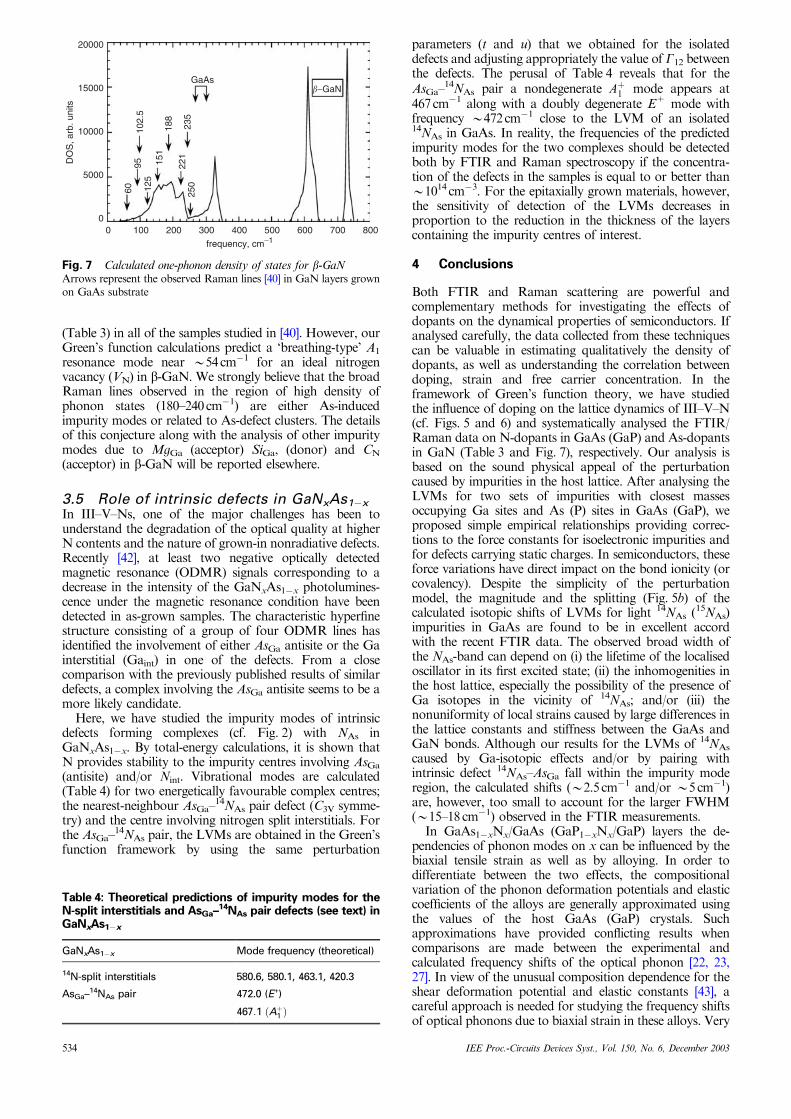
used Green’s function theory and calculated the impuritymodes of AsN in b–GaN by solving (5) (Table 3).The perusal of Table 3 reveals that five of the Raman linesnear 94cm�1 (11.9meV), 125cm�1 (15.6meV), 151cm�1
(18.7meV), 235cm�1 (29.4meV) and 250cm�1 (31.2meV),are in good agreement with the calculated impurity modesfor isolated AsN. It is also worth mentioning that four of thelines near 18.9, 23.7, 27.4 and 29.4meV fall in the acousticalmode region where the density of phonon states is high(Fig. 7) and two of the weaker Raman features near B60(7.5meV) and 102cm�1 (12.8meV) are not observed
Table 2: Exploring the possibility of Ga isotopic masses involved in different nearest-neighbour configurations of theGaAs:14N system responsible for a larger FWHM of the N-local mode
System Symmetry Modes Probability factor for each LVM withC¼0.604
69Ga4�14N Td F2 C4 0.13369Ga3�14N�71Ga1 C3v A1, E 4
Considering the abundance of the 69Ga as 60.4 at.%, the probability of the LVMs appearing in each configuration is also given. The shift inLVMs of 14NAs caused by Ga isotopes is B2.5cm�1 which is too small to account for the larger FWHM B18cm�1 observed in the FTIRmeasurements [21].
Table 3: Comparison of calculated and experimental in-band modes of ASN (Td symmetry) in b-GaN
System Mode frequency (cm�1)
Modetype
Theoretical Experimental* u, relativechange inforce constant
b-GaN: As 60 (w) 0.18
F2 94 95 (s)
102 (w)
A1 128 125 (s)
F2 154 151 (s)
188 (b)
221 (s)
A1 231 235 (b)
F2 256 250 (s)
*From [40]Terms (w), (s), and (b) describe weak, sharp, and broad lines,respectively, in the Raman studies after [40]
(Table 3) in all of the samples studied in [40]. However, ourGreen’s function calculations predict a ‘breathing-type’ A1
resonance mode near B54cm�1 for an ideal nitrogenvacancy (VN) in b-GaN. We strongly believe that the broadRaman lines observed in the region of high density ofphonon states (180–240cm�1) are either As-inducedimpurity modes or related to As-defect clusters. The detailsof this conjecture along with the analysis of other impuritymodes due to MgGa (acceptor) SiGa, (donor) and CN
(acceptor) in b-GaN will be reported elsewhere.
3.5 Role of intrinsic defects in GaNxAs1�xIn III–V–Ns, one of the major challenges has been tounderstand the degradation of the optical quality at higherN contents and the nature of grown-in nonradiative defects.Recently [42], at least two negative optically detectedmagnetic resonance (ODMR) signals corresponding to adecrease in the intensity of the GaNxAs1�x photolumines-cence under the magnetic resonance condition have beendetected in as-grown samples. The characteristic hyperfinestructure consisting of a group of four ODMR lines hasidentified the involvement of either AsGa antisite or the Gainterstitial (Gaint) in one of the defects. From a closecomparison with the previously published results of similardefects, a complex involving the AsGa antisite seems to be amore likely candidate.Here, we have studied the impurity modes of intrinsic
defects forming complexes (cf. Fig. 2) with NAs inGaNxAs1�x. By total-energy calculations, it is shown thatN provides stability to the impurity centres involving AsGa(antisite) and/or Nint. Vibrational modes are calculated(Table 4) for two energetically favourable complex centres;the nearest-neighbour AsGa–
14NAs pair defect (C3V symme-try) and the centre involving nitrogen split interstitials. Forthe AsGa–
14NAs pair, the LVMs are obtained in the Green’sfunction framework by using the same perturbation
parameters (t and u) that we obtained for the isolateddefects and adjusting appropriately the value of G12 betweenthe defects. The perusal of Table 4 reveals that for theAsGa–
14NAs pair a nondegenerate Aþ1 mode appears at
467cm�1 along with a doubly degenerate E+ mode withfrequency B472cm�1 close to the LVM of an isolated14NAs in GaAs. In reality, the frequencies of the predictedimpurity modes for the two complexes should be detectedboth by FTIR and Raman spectroscopy if the concentra-tion of the defects in the samples is equal to or better thanB1014 cm�3. For the epitaxially grown materials, however,the sensitivity of detection of the LVMs decreases inproportion to the reduction in the thickness of the layerscontaining the impurity centres of interest.
4 Conclusions
Both FTIR and Raman scattering are powerful andcomplementary methods for investigating the effects ofdopants on the dynamical properties of semiconductors. Ifanalysed carefully, the data collected from these techniquescan be valuable in estimating qualitatively the density ofdopants, as well as understanding the correlation betweendoping, strain and free carrier concentration. In theframework of Green’s function theory, we have studiedthe influence of doping on the lattice dynamics of III–V–N(cf. Figs. 5 and 6) and systematically analysed the FTIR/Raman data on N-dopants in GaAs (GaP) and As-dopantsin GaN (Table 3 and Fig. 7), respectively. Our analysis isbased on the sound physical appeal of the perturbationcaused by impurities in the host lattice. After analysing theLVMs for two sets of impurities with closest massesoccupying Ga sites and As (P) sites in GaAs (GaP), weproposed simple empirical relationships providing correc-tions to the force constants for isoelectronic impurities andfor defects carrying static charges. In semiconductors, theseforce variations have direct impact on the bond ionicity (orcovalency). Despite the simplicity of the perturbationmodel, the magnitude and the splitting (Fig. 5b) of thecalculated isotopic shifts of LVMs for light 14NAs (
15NAs)
impurities in GaAs are found to be in excellent accordwith the recent FTIR data. The observed broad width ofthe NAs-band can depend on (i) the lifetime of the localisedoscillator in its first excited state; (ii) the inhomogenities inthe host lattice, especially the possibility of the presence ofGa isotopes in the vicinity of 14NAs; and/or (iii) thenonuniformity of local strains caused by large differences inthe lattice constants and stiffness between the GaAs andGaN bonds. Although our results for the LVMs of 14NAs
caused by Ga-isotopic effects and/or by pairing withintrinsic defect 14NAs–AsGa fall within the impurity moderegion, the calculated shifts (B2.5 cm�1 and/or B5 cm�1)are, however, too small to account for the larger FWHM(B15–18cm�1) observed in the FTIR measurements.In GaAs1�xNx/GaAs (GaP1�xNx/GaP) layers the de-
pendencies of phonon modes on x can be influenced by thebiaxial tensile strain as well as by alloying. In order todifferentiate between the two effects, the compositionalvariation of the phonon deformation potentials and elasticcoefficients of the alloys are generally approximated usingthe values of the host GaAs (GaP) crystals. Suchapproximations have provided conflicting results whencomparisons are made between the experimental andcalculated frequency shifts of the optical phonon [22, 23,27]. In view of the unusual composition dependence for theshear deformation potential and elastic constants [43], acareful approach is needed for studying the frequency shiftsof optical phonons due to biaxial strain in these alloys. Very
15000
10000
20000
5000
00
DO
S, a
rb. u
nits
100 200 300 400 500 600 700 800
frequency, cm−1
6095
125
151
221
250
235
188
102.
5
GaAs�−GaN
Fig. 7 Calculated one-phonon density of states for b-GaNArrows represent the observed Raman lines [40] in GaN layers grownon GaAs substrate
Table 4: Theoretical predictions of impurity modes for theN-split interstitials and AsGa–
recently, Goldman et al. [44] studied stress evolution inGaAs1�xNx films using a combination of in-situ and ex-situmeasurements. They have found evidence for significantnon substitutional (mostly interstitial) N incorporation forxZ0.015. Based on total energy calculations, the presenceof an isolated N-interstitial (Nint) in GaAs1�xNx is quiteunlikely at higher compositions (x40.015). However, theformation of the nonradiative microstructures involving Nand/or intrinsic defects are energetically favourable. In theepitaxially grown GaNxAs1�x/GaAs (xr0.03} samples, thepredicted impurity mode frequencies of the N split-interstitials and AsGa–
14NAs pair should be detected byFTIR and Raman spectroscopy provided the concentrationof defect centres in the MBE-grown materials is equal to orbetter than B1014 cm�3.Our Green’s function calculations for the vibrational
properties of heavier AsN impurities in b-GaN comparefavourably with the Raman data on GaN layers grown onGaAs substrates as well as on GaN samples intentionallydoped with As [40]. On the cation/anion sites in GaN(Fig. 6), the other dopants of interest are BeGa (a
�), BGa (i),AlGa (i), MgGa (a
�), and SiGa (d+)/CN (a�). In the absence
of experimental data, we have predicted the possibilities ofLVMs as well as gap modes as a function of t for some ofthese defects. If the changes in force constants for suchdefects in GaN are assumed to be the same as in GaAs,then the vibrational modes of these dopants will exhibitstrong hybridisation with the optical phonons of the hostlattice. This might be the reason why local modes of Si, Mgand Al, etc. in GaN have not been reported in the literatureeither by FTIR or by Raman spectroscopy.
5 Acknowledgments
The work performed at Indiana University of Pennsylvaniawas supported in part by the grants from National ScienceFoundation (NSF: ECS-9906077) and Research Corpora-tion (Cottrell College Science Award #CC 4600). Theauthor has benefitted from very fruitful discussions on thesubject matter with Prof. B. M. Arora of Tata Institute ofFundamental Research, Mumbai, India; Dr. D. Look ofthe Wright State University, Dayton, Ohio; and Prof. A. R.Adams of the University of Surrey, UK.
6 References
1 Ager, J.W. III, and Walukiewicz, W.: ‘Current status of research anddevelopment of III–V–N semiconductor alloys’, Semicond. Sci.Technol., 2002, 17, pp. 741–745
2 Welty, R.J., Xin, H.P., Mochizuki, K., Tu, C.W., and Asbeck, P.M.:‘GaAs/Ga0.89In0.11N0.02As0.98/GaAs NpN double heterojunctionbipolar transistor with low turn-on voltage’, Solid-State Electron.,2002, 46, pp. 1–5
3 Buyanova, I.A., Chen, W.M., and Monnar, B.: ‘Electronic propertiesof Ga(In)NAs alloys’, MRS Internet J. Nitride Semicond. Res., 2001,6, pp. 2–19
4 Tu, C.W.: ‘III-N-V low bandgap nitrides and their device applica-tions’, J. Phys., Condens. Matter, 2001, 13, pp. 7169–7182
5 Brinkman, W.F., Koch, T.L., Lang, D.V., and Wilt, D.P.: ‘The lasersbehind the communications revolution’, Bell Labs Tech. J., Jan.–Mar.2000, pp. 150–166
6 Harris, J.S., Jr., and Gambin, V.: ‘GaInNAs : a new material in thequest for communication lasers’, Mater. Res. Soc. Symp. Proc., 2002,722, pp. 117–133
8 Fischer, M., Gollub, D., Reinhardt, M., and Forchel, A.: ‘Advances inGaInNAs edge emitting laser diodes’. Presented at 8th Micro-opticsConf. (MOC ‘01), M4, Osaka, Japan, 2001
9 Barnham, K.W.J., Abbott, P., Ballsrd, I., Bushnell, D.B., Chatten,A.J., Mazzer, M., Hills, G., Roberts, J.S., Malik, M.A., and O’Brien,P.: ‘Future applications of low dimensional structures in photo-voltaics’, Electrochem. Soc. Proc., 2001, 10, pp. 30–46
10 Allerman, A.A., Follstaedt, D.M., Gee, J.M., Jones, E.D., Kurtz,S.R., and Modine, N.A.: ‘InGaAsN: a novel material for high-
efficiency solar cells and advanced photonic devices’. Sandia NationalLab Rep. SAND 99-0922
11 Kaplar, R.J., Kwon, D., Ringel, S.A., Allerman, A.A., Kurtz, S.R.,and Jones, E.D.: ‘Deep levels in p and n-type InGaAsN for highefficiency multi-junction III-V cells’, Sol. Energy Mater. Sol. Cells,2001, 66, pp. 85–91, (http://www.nrel.gov/ncpv/pdfs/tsuo.pdf)
12 Kaplar, R.J., Ringel, S.A., Kurtz, S.R., Klem, J.F., and Allerman,A.A.: ‘Deep-level defects in InGaAsN grown by molecular-beamepitaxy’, Appl. Phys. Lett., 2002, 80, pp. 1–4
14 Kaplar, R.J., Arehart, A.R., Ringel, S.A., Allerman, A.A., Sieg, R.M.,and Kurtz, S.R.: ‘Deep levels and their impact on generation currentin Sn-doped InGaAsN’, J. Appl. Phys., 2001, 90, pp. 3405–3408
15 Kurtz, S., Webb, J., Gedvilas, L., Friedman, D., Geisz, J.,Olson, J., King, R., Joslin, D., and Karam, N.: ‘Structural changesduring annealing of GaInAsN’, Appl. Phys. Lett., 2001, 78,pp. 748–750
16 Xin, H.P., Welty, R.J., and Tu, C.W.: ‘GaNP/GaP double-hetero-structure red light-emitting diodes directly grown on GaP substrates’,IEEE Photonics Technol. Lett., 2000, 12, pp. 960–962
17 Baldassarri, G., Bissiri, H.V. H. M., Polimeni, A., Capizzi, M.,Fischer, M., Reinhardt, M., and Forchel, A.: ‘Hydrogen-induced bandgap tuning of InGaAsN/GaAs single quantum wells’, Appl. Phys.Lett., 2001, 78, pp. 3472–3474
18 Polimeni, A., Baldassarri, G., Bissiri, H.V. H.M., Capizzi, M., Fischer,M., Reinhardt, M., and Forchel, A.: ‘Effect of hydrogen on theelectronic properties of InxGa1�xAs1�yNy/GaAs quantum wells’,Phys. Rev. B, Condens. Matter., 2001, 63, p. R201304
19 Kozhevnikov, M., Narayanamurti, V., Reddy, C.V., Xin, H.P., Tu,C.W., Mascarenhas, A., and Zhang, Y.: ‘Evolution of GaAs1�xNx
conduction states and giant Au/GaAs1�xNx Schottky barrier reduc-tion studied by ballistic electron emission spectroscopy’, Phys. Rev. B,Condens. Matter., 2000, 61, pp. R7861–7864
20 Kitani, T., Kondow, M., Kikawa, T., Yazawa, Y., Okai, M., andUomi, K.: ‘Analysis of band offset in GaNAs/GaAs by X-rayphotoelectron spectroscopy’, Jpn. J. Appl. Phys., 1999, 38, p. 5003
21 Alt, H.CH., Egorov, A.YU., Riechert, H., Wiedemann, B., Meyer,J.D., Michelmann, R.W., and Bethge, K.: ‘Infrared absorption studyof nitrogen in N-implanted GaAs and epitaxially grown GaAs1-xN(x)layers’, Appl. Phys. Lett., 2000, 77, pp. 3331–3333
22 Leibiger, G., Gottschalch, V., Schwabe, R., Bendorf, G., andSchubert, M.: ‘Phonon modes and critical points of GaPN’, Phys.Status Solidi B, 2001, 228, pp. 279–282
23 Leibiger, G., Gottschalch, V., Schwabe, R., Bendorf, G., andSchubert, M.: ‘Phonon modes of GaN(y)P(1�y) (0.006ryr0.0285)measured by midinfrared spectroscopic ellipsometry’, Appl. Phys.Lett., 2001, 79, pp. 3407–3409
24 Leibiger, G., Gottschalch, V., Rheinl.ander, B., $Sik, J., and Schubert,M.: ‘Model dielectric function spectra of GaAsN for far-infrared andnear-infrared to ultraviolet wavelengths’, J. Appl. Phys., 2001, 89,pp. 4927–4938
25 Prokofyeva, T., Sauncy, T., Seon,M., Holtz, M., Qiu, Y., Nikishin, S.,and Temkin, H.: ‘Raman studies of nitrogen incorporation inGaAs1�xNx’, Appl. Phys. Lett., 1998, 73, pp. 1409–1411
26 Soni, R.K., Katiyar, R.S., Asahi, H., Tampo, H., and Gonda, S.:‘Raman scattering in GaN-rich ternary GaNP alloys’. Proc. Int. 17thConf. on Raman spectroscopy, Peking University, Beijing, China, 20–25 August 2000
27 Buyanova, I.A., Chen, W.M., Xin, H.P., and Tu, C.W.: ‘Disorder-activated resonant Raman scattering in GaNAs/GaAs structures’.Proc. 25th Int. Conf. on the Physics of semiconductors, Osaka, Japan,17–22 Sept. 2000
28 Buyanova, I.A., Chen, Goldys, E.M., Xin, H.P., and Tu, C.W.:‘Structural properties of a GaNxP(1-x) alloy: Raman studies’, Appl.Phys. Lett., 2001, 78, pp. 3959–3961
29 Seong, M.J., Hanna, M.C., and Mascarenhas, A.: ‘Compositiondependence of Raman intensity of the nitrogen localized vibrationalmode in GaAs1�xNx’, Appl. Phys. Lett., 2001, 79, pp. 3974–3976
30 Cheong, H.M., Zhang, Y., Mascarenhas, A., and Geisz, J.F.:‘Nitrogen-induced levels in GaAs1�x Nx studied with resonant Ramanscattering’, Phys. Rev. B, Condens. Matter, 2000, B61, pp. 13687–13690
31 Baroni, S., De Girncoli, S., Dal Corso, A., and Gianozzi, P.: ‘Phononsand related crystal properties from density-functional perturbationtheory’, Rev. Mod. Phys., 2001, 73, pp. 515–562
32 Talwar, D.N.: ‘Site selectivity of defects in III-V compounds by localmode spectroscopy and model calculations’, in Di Bartolo, B.and Chen, X. (Eds.): ‘Advances in energy transfer processes’ (WorldScientific, 2001), p. 487
33 Talwar, D.N.: ‘Dispersion of optical and acoustical phonons in thezinc-blende group III-nitride superlattices’, Microelectron. Eng., 1998,43–44, pp. 309–318
34 Harrison, W.A.: ‘Electrical structure and the properties of solids – thephysics of chemical bond’ (Dover, 1980)
35 Karch, K., Wagner, J.M., and Bechstedt, F.: ‘Ab initio study ofstructural, dielectric and dynamical properties of GaN’, Phys. Rev. B,Condens. Matter, 1998, B57, pp. 7043–7049
36 Strauch, D., and Dorner, B.: ‘Phonon dispersion in GaAs’, J. Phys.,Condens. Matter, 1990, 2, pp. 1457–1474
37 Yarnell, J.L., Warren., J.L., and Wenzer, R.G.: ‘Neutron inelasticscattering’ (IAEA, Vienna, 1968), Vol. 1, p. 301
38 Ramsteiner, M., Menninger, J., Brandt, Yang, O.H., and Ploog, K.H.:‘Shallow donors in GaN studied by electronic Raman scattering inresonance with yellow luminescence transitions’, Appl. Phys. Lett.,1996, 69, pp. 1276–1278
39 Jiang De-Sheng, Ramsteiner, M., Ploog, K.H., Tews, H.,Graber, A., Averbeck, R., and Riechert, H.: ‘Defect-induced Ramanscattering in resonance with yellow luminescence transitions inhexagonal GaN on a sapphire substrate’, Appl. Phys. Lett., 1998,72, pp. 365–367
40 Siegle, H., Kaschner, A., Hoffman, A., Broser, I., and Thomsen, C.:‘Raman scattering from defects in GaN: the question of vibrational or
41 Wagner, J., K.ohler, K., Ganser, P., and Herres, N.: ‘GaAsNinterband transitions involving localized and extended states probedby resonant Raman scattering and spectroscopic ellipsometry’, Appl.Phys. Lett., 2000, 77, pp. 3592–3594
42 Thinh, N.Q., Buyanova, I.A., Hai, P.N., Chen, W.M., Xin, H.P., andTu, C.W.: ‘Signature of an intrinsic point defect in GaNxAs1�x’, Phys.Rev. B, Condens. Matter, 2001, B63, p. 033203
43 Zhang, Y., Mascarenhas, A., Xin, H.P., and Tu, C.W.: ‘Valence-bandsplitting and shear deformation potential of dilute GaAs1�xNx alloys’,Phys. Rev. B, Condens. Matter, 2000, B61, pp. 4433–4436