NASA/TP-2000-210096 Characterization of Advanced Avalanche Photodiodes for Water Vapor Lidar Receivers Tamer F. Refaat Old Dominion University, Norfolk, Virginia Gary E. Halama and Russell J. DeYoung Langley Research Center, Hampton, Virginia July 2000 https://ntrs.nasa.gov/search.jsp?R=20000075199 2020-04-02T23:04:09+00:00Z
Development of advanced differential absorption lidar (DIAL)
receivers is very important to increase the accuracy of atmospheric
water vapor measurements. A major component of such receivers is
the optical detector. In the near-infrared wavelength range avalanche
photodiodes (APD's) are the best choice for higher signal-to-noise
ratio, where there are many water vapor absorption lines. In this
study, characterization experiments were performed to evaluate a
group of silicon-based APD's. The APD's have different structures
representative of different manufacturers. The experiments include set-
ups to calibrate these devices, as well as characterization of the effects
of voltage bias and temperature on the responsivity, surface scans,
noise measurements, and frequency response measurements. For each
experiment, the setup, procedure, data analysis, and results are givenand discussed. This research was done to choose a suitable APD
detector for the development of an advanced atmospheric water vapor
differential absorption lidar detection system operating either at
720, 820, or 940 rim. The results point out the benefits of using the
super low ionization ratio (SLIK) structure APD for its lower
noise-equivalent power, which was found to be on the order of 2 to
4 fW/Hz 1/2, with an appropriate optical system and electronics. The
water vapor detection systems signal-to-noise ratio will increase by a
factor of lO.
1. Introduction
Water vapor is an important molecular species in the Earth's atmosphere, which is primarily located
in the troposphere (part of the atmosphere extending from the surface of the Earth to an altitude of about
18 kin). Although the distribution of atmospheric water vapor is highly variable in both time and loca-
tion, its measurement is very important for understanding the Earth's water cycle, greenhouse effect,
and weather phenomena (refs. 1 and 2).
The water cycle involves interactions among the Earth's global systems; the atmosphere, hydro-
sphere, cryosphere, lithosphere, and biosphere. Water is considered the main media for energy transfer
between most of these systems. Although the amount of atmospheric water vapor represents only a
small percent of the Earth' s water reservoir, it is very dynamic and its latent heat transformation is con-
sidered the main energy source that maintains the atmospheric general circulation (refs. 1 and 2).
Water vapor and clouds affect the incident solar radiation by reflecting solar radiation back to space
and also absorbing some of this energy within the atmosphere, which substantially moderates the
Earth's climate. On the other hand, water vapor and clouds affect infrared radiation released by theEarth's surface. Some of this radiation is reflected back to the surface and some is absorbed and reemit-
ted at a lower temperature which contributes to the global warming problem or greenhouse effect
(ref. 2).
Water vapor has a direct role in most weather phenomena and natural disasters such as hurricanes.
The latent heat of water vapor was found to be the main energy source for hurricanes (ref. 3). The mea-
surement of water vapor flow into a hurricane associated with other observations aids in estimating the
hurricanedirectionandstrength(ref.3).Therefore,theinterestin measuringatmosphericwatervaporhasincreased and leads to developing various techniques to accurately measure its density.
1.1. Water Vapor Measurement
Several techniques are used to measure atmospheric water vapor such as balloon radiosondes, air-
craft in situ, and ground- or aircraft-based laser remote sensing. For global measurement of the distribu-
tion of water vapor, the most effective method is space-based laser remote sensing. A future goal is to
apply laser remote sensing on a space-based platform to continuously measure the water vapor density
of the Earth (ref. 4).
Laser remote sensing is a technique used for measuring a molecular density without any physical
contact between the sensing device and the atmospheric molecule under observation. It is basically used
for applications where direct measurement is very difficult to achieve because of large distances. The
technique usually is reliable and fast and does not disturb the measured quantity. Two main classes of
laser remote sensing systems are routinely used. One uses the Raman technique and the other uses dif-
ferential absorption lidar (DIAL) (ref. 4). In the Raman technique, the laser radiation is scattered inelas-
tically from the observed molecule with a frequency shift characteristic of the molecule. The
disadvantage of this technique is the complexity of the Raman spectrum. The DIAL technique is more
typically used because it is a relatively simpler measurement with higher accuracy (refs. 4, 5, and 6).
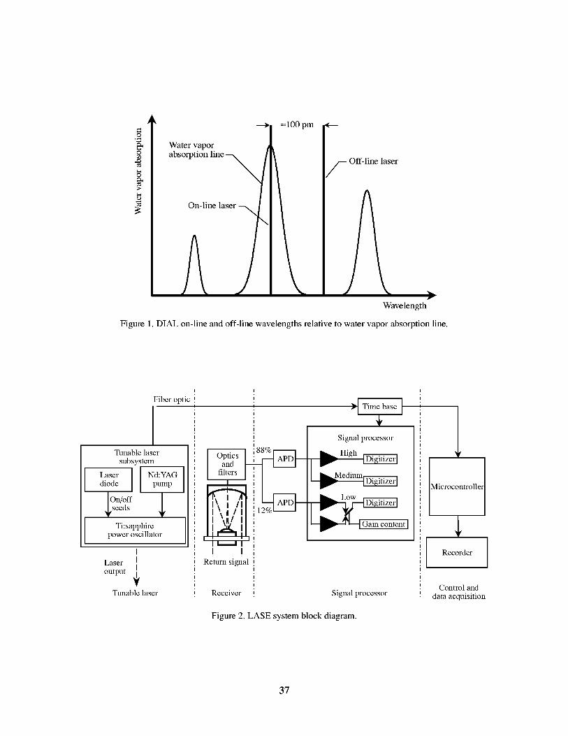
1.2. DIAL Technique for Measuring Water Vapor
Light detection and ranging (lidar) is an active remote sensing technique which uses a pulsed laser
and a colocated receiver to measure the density of atmospheric gases and aerosols as a function of
range. In the DIAL technique, two laser pulses at slightly different wavelengths are transmitted into the
atmosphere. The transmitted laser pulses are subjected to scattering and absorption because of the mol-
ecules and particles in the atmosphere; therefore, the light backscattered to a telescope receiver contains
some information about these molecules and particles which can be evaluated by using the lidar equa-
tion (refs. 4, 6, 7, and 8).
When looking at the lidar signals in terms of the received power and if the transmitted laser pulse
has an initial optical power Po, the backscattered received power from a range r is given by (refs. 7and 8)
Usingequation(1) to formaratioof theon-andoff-powerreturnsallowstheability to measurewatervaporasafunctionof range.If thewavelengthdifferencebetweentheon-lineandtheoff-linesignalsis lessthan0.1nm,_on(r)= _off(r)andkon(r) = kof f (r) can be assumed, and the number density
where r 2 - r 1 is the range cell for the average concentration, (Yon - (Yoff is the differential absorption
cross section for the two wavelengths, Pon is the power received from range r for the on-line wave-
length, and Poff is the power received from range r for the off-line wavelength. One can then convert thenumber density profile to a mass mixing ratio by dividing the gas number density by the ambient
atmospheric number density (refs. 4, 7, and 8).
2. Background
A critical component in any remote sensing technique is the detector. Water vapor DIAL detection
systems typically use avalanche photodiodes (APD's). Compared with a photomultiplier tube (PMT),
an APD is much more compact, lightweight, and mechanically rugged and has a lower bias voltage
which is suitable for compact size detection systems. Also, an APD has higher quantum efficiency close
to 90 percent at wavelengths of 720, 820, and 940 nm, which are water vapor DIAL absorption bands of
interest where PMT quantum efficiency is usually very low. APD's typically use a lower bias voltage
(hundred of volts) than is required for a PMT (kilovolt range) (refs. 9 and 10).
Compared with p-i-n photodiodes, APD's include an internal gain mechanism which increases their
signal-to-noise ratio (SNR). APD's have excellent linearity with respect to incident light intensity. Withsome structures, an APD can have very low noise in the range of a few fW/Hz 1/2. For these reasons,
water vapor DIAL detection systems use APD's to measure the backscattered light signals (refs. 10
to 13).
2.1. Lidar Atmospheric Sensing Experiment
The lidar atmospheric sensing experiment (LASE) is shown in the block diagram of figure 2. LASE
is an instrument that detects water vapor by using the 815-nm water vapor absorption line. LASE mea-
surements were found to have an accuracy better than 6 percent or 0.01 g/kg, whichever is greateracross the entire troposphere (refs. 14 and 15).
The LASE transmitter was designed to generate two laser pulses of 30 ns duration each separated by
400 bts at a frequency of 5 Hz with a pulse energy output of 150 mJ. A Ti:sapphire (Ti:A1203) power
oscillator was constructed with an Nd:YAG laser as the pump source. Narrow line width and wave-
length tuning of the Ti:A1203 laser is achieved by a continuous-wave 100-mW single mode diode laser
performing as an injection seed source. This injected seeding allows control of the spectral line width to
within 1 pm and provides wavelength tuning stability to _+0.25 pm. The diode laser wavelength is locked
TheAPDdetectoroutputsignalis appliedto a transimpedanceamplifierstagewhichlimits thesignalbandwidthto 2.5MHz.A 1.5-MHzlow-passfilter is usedto setthesignalbandwidth,thenthesignalsareappliedto 12-bit,10-MHzdigitizers.Boththeamplifierandthedigitizerstagesaremountedin a CAMAC(computerautomatedmeasurementsandcontrol)cratewhichcommunicateswith anonboardcomputerfor datarecording.Thewholesystemis synchronizedby a time-basedgeneratedtriggersignal(ref.14).
The main goal of this research is to increase the signal-to-noise ratio of the water vapor DIAL detec-
tion system by a factor of 10 compared with the current LASE detection system. Also, the system must
be compact in size suitable for placing it directly on the receiver telescope. These goals are achievable
with state-of-the-art electronic components, a newly evaluated very low noise APD detector, and the
construction of a 14-bit, 10-MHz waveform digitizer, which will be placed as close as possible to this
detector (refs. 17 to 20). The new DIAL receiver system is shown schematically in figure 3. The analog
circuit will condition the APD output signal and also control its bias voltage and temperature; the digital
circuit will convert the analog signal into a digital form. The basis for the APD selection is discussed.
3. Avalanche Photodiodes
APD's are solid state quantum detectors suitable for low light detection in the visible and near infra-
red regions. These devices are commercially available from many manufacturers and are fabricated with
different solid state structures. They have several applications including backscatter lidar, DIAL, and
fiber-optic communication. Although they are widely used, few papers in the literature have discussedtheir characterization.
3.1. APD Structure and Theory of Operation
The basic structures of a p-i-n diode and three other APD's and their electric field distribution are
shown in figure 4. The p-i-n diode shown in figure 4(a) is a p-n junction with an intrinsic or lightly
doped layer sandwiched between the p and n layers. This structure serves to extend the width of the
depletionregionwhichincreasesthevolumeavailablefor absorbingthe incidentphotons.Also itreducesthejunctioncapacitance;thereby,theRC time constantis reduced,whichresultsin higherdetectionbandwidth.Thustheresponsetimeof thesedevicesis in therangeof tensof picoseconds,whichcorrespondsto bandwidthsof gigahertz(refs.10to 13).A disadvantageof p-i-ndetectorsis thattheyhaveno internalgainmechanism.TheAPDstructure,similarto thep-i-ndiodestructure,hasagainmechanismwithin the devicecalledthe impactionizationprocessin whichthephotoelectricchargecarriers,becauseoftheirhighenergy,canimpactandcauseionizationof latticeatomsleadingtoanavalanchebreakdownor internalgain(refs.10to 13and21).
Asshownin figure4(b)thebeveled-edgeAPDhasthesimpleststructureof theonesused.It con-sistsof a p+-njunctionwith a highresistivityn layerwhichincreasesthebreakdownvoltageof thedeviceinto therangeof kilovolts.Breakdownat theedgesis preventedbybevelingandmakingthejunctionverydeepin therangeof 50 btm. Therefore, the dead part of the p+ layer is usually etched away
to reduce the device depth. Because the n layer is much deeper than the p+ layer, electrons produced
there are more likely to be multiplied than holes. This reduces the dark-current noise which is mostly
generated by hole current. The disadvantage, however, is that only light absorbed in the p layer leads to
effective multiplication, and this layer has the lowest electric field. Therefore, charge accumulates
slowly, which leads to a longer response time typically in the range of tens of nanoseconds (ref. 21).
The reach-through structure APD with its electric field distribution is shown in figure 4(c). This
structure consists of an absorption region and, separated from it, a multiplication region. In the absorp-
tion region, the p+ layer at the active surface is followed by an intrinsic wide layer, which increases the
photon absorption depth. The emitted photoelectrons drift and reach a constant velocity. In the multipli-
cation region, the p-n + layers form a thin junction with a high internal field, which enhances the impact
ionization process (refs. 21, 22, and 23). Recently, an enhancement of the reach-through structure,
known as the "super low ionization ratio _:" (SLIK) geometry, has become available and is shown in
figure 4(d) (ref. 24). The ability of electrons and holes to "impact ionize" to generate additional charge
carriers is characterized by the ionization coefficients czand [3 for electrons and holes, respectively. The
ionization coefficient represents the ionization probabilities per unit length. An important parameter is
the ionization ratio _:given by
In APD's, it is desirable to reduce _: as much as possible so that the multiplication process is only due to
electrons, since hole current leads to high dark-current noise (ref. 10). This reduction was achieved in
the SLIK structure by increasing the absorption region electric field and merging this region with the
multiplication region (ref. 24). Typically, the value of _: is in the range of 0.02 for the reach-through
structure, whereas it is 0.002 for the SLIK structure (ref. 24). The structure types and the manufacturer's
data for the characterized APD's are given in appendix A.
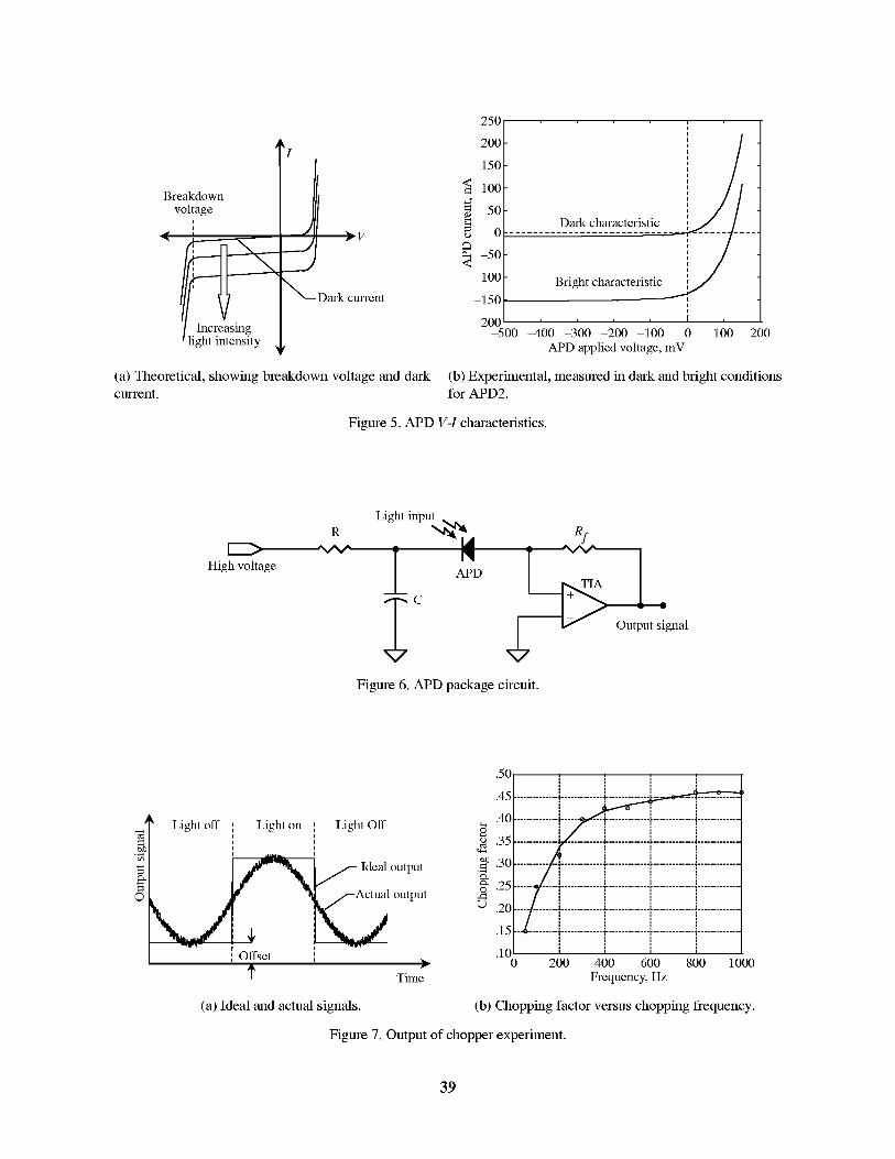
3.2. APD Characteristics and Applied Circuit
An APD with no incident light has V-I characteristics similar to a rectifier diode as shown theoreti-
cally in figure 5(a). However, when the device absorbs photons due to incident light, the characteristics
will be shifted downward. Fortunately, this shift is highly linear with the intensity of the absorbed light.
Furthermore,thenewshiftedcurvesareparallelwith theoriginalcurvesasshownin figure5(b).TheV-I relation of the device can be given by (refs. 10 and 11)
I = Is(e qv/kT- 1]-I d (4)
where I is the current through the device, I s is the saturation current, q is the electron charge, V is theapplied voltage, k is the Boltzmann constant, and T is the temperature. Equation (4) resembles the diode
equation with the first term representing the dark current and the additional term I d representing thephotocurrent given by (refs. 10 and 11)
I d = qG _c _'P (5)
where q is the quantum efficiency, G is the APD internal gain, h is Planck constant, c is the light speedin vacuum, _ is the incident light wavelength, and P is the incident optical power. By knowing the APD
sensitive area A, the optical power can be related to the light intensity I (W/m 2) by
P = IA (6)
By definition the detector responsivity 9_ (A/W) can be obtained from equation (5) and is defined by
(refs. 10 and 11)
I d (19_ - - qG _ _ (7)
P //6'
Because APD's can source current through the internal photoeffect, they may operate without the
need of an external power source. However, speed of response and gain can be improved by using an
externally applied bias voltage. Thus, in most applications an external reverse voltage bias is applied to
the APD. The APD current variation, representing the change in the light intensity, is then converted to
a voltage variation by a current-to-voltage converter or transimpedance amplifier (TIA). This configura-
tion is shown in figure 6 where R is the amplifier feedback resistance, and R and C act as a low-passf
filter which eliminates any bias voltage ripple noise. A disadvantage of this technique is the additional
noise associated with the TIA as well as the limitation in the frequency response (refs. 10 and 25).
4. Responsivity Calibration
The APD spectral response was measured over a wavelength range from 600 to 1100 nm by com-
parison with a reference detector calibrated by the NIST (National Institute of Standards and Technol-
ogy. (See appendix B.) Each detector was placed in the same uniform light field at the same position;
this allowed the APD's to be calibrated at certain wavelengths in the specified range. Because the APD
response is dependent on its bias voltage and temperature, both dependencies were characterized rela-
tive to the reference detector and were maintained constant during the calibration. At each wavelength,
the test APD responsivity 9_d was calculated by substituting equation (6) into (7) to obtain
I d(8)
_d - 1Ad
where I d and A d are the test APD output current and sensitive area, respectively, and I is the intensity
of the uniform field. The light intensity can be obtained from
11 .
I - (9)9irA r
where I r is the reference detector output current, A r is the sensitive area, and _Rr is the responsivity at
the same wavelength. Combining equations (8) and (9) gives
I d A r
% - -i7,. % (lO)
Furthermore, the test and reference detector output currents were determined by dividing the feed-
back resistance into the measured voltage output of a TIA. Substituting this result into equation (10)results in
V d R r A r(11)
where R r and R d are the feedback resistances for the reference and test detectors, respectively, and V r
and Vcl are the TIA output voltages for the reference and test detectors, respectively.
As indicated from equation (4), the APD output signal is associated with a dc offset due to its dark
current. Another offset is also added due to the background and thermal radiation. A good practice in
such experiments is to use an optical chopper to modulate the input light signal to the detector. The dc
offsets can then be eliminated with a high-pass filter at the APD output. This technique allows one to
measure very small photocurrents in a range of nanoamperes with sensitive instruments such as lock-in
amplifiers. In this case, the chopping factor CF must be considered for correcting the APD output read-
ing obtained from this instrument Vlock in to its peak-to-peak value Vp_ which is the true indication ofthe light intensity. Thus, the chopping factor is given by
Vlock inCF-
Vp p(12)
Because of ac coupling, the operating frequency of the chopper is chosen to maximize the output
signal. The typical chopped output response and that of the ideal square wave response are shown in
figure 7(a). A good practice is to obtain the variation of the chopping factor against the chopping
frequency as shown in figure 7(b). For this particular case, the chopping factor was maximized at
frequencies above 700 Hz.
If CF r and CF d are the chopping factors for the reference and test detectors, respectively, equa-
tion (11) can be modified to
(Vd)lockin CF r R r A r(13)
Equation (13) was used for absolute calibration of the tested APD's in terms of the calibrated referencedetector.
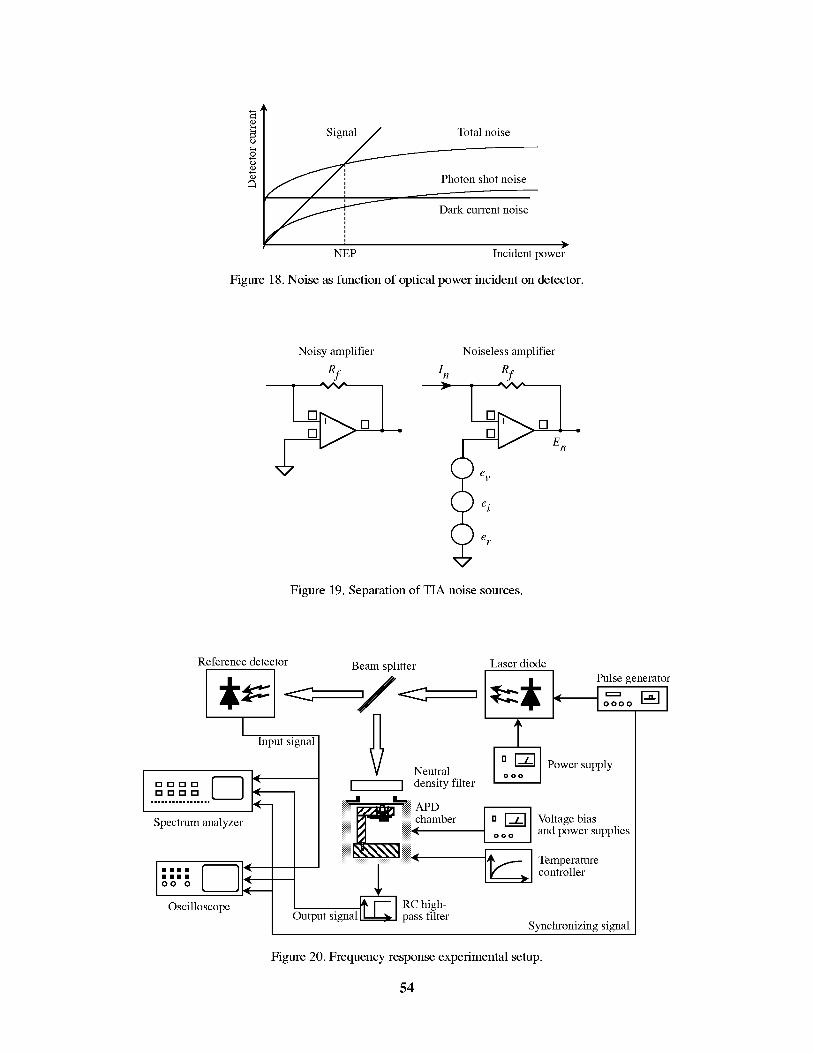
4.1. Experimental Setup
The experimental setup for the APD responsivity calibration is shown in figure 8. The light source
was a halogen lamp supplied by a stabilized power supply to ensure a stable spectrum and intensity. The
lamp output was filtered by a 600-nm high-pass filter to prevent higher order dispersion of shorter
wavelengths from being collected in first-order dispersion in the range of 600 to 1100 nm. The chopper
was used to modulate the optical signal. For most of the APD's, a 200-Hz chopping frequency was suf-
ficient to optimize the chopping factor. The monochromator was used to separate the light input into its
spectral components. An integrating sphere was used to diffuse the exiting light to ensure intensity uni-
formity at the detector, which is especially important for large area detectors. A disadvantage of using
the integrating sphere is the considerable reduction in light intensity. For small area detectors, where a
higher intensity was required, the integrating sphere was replaced by a diffuser; or in some cases, the
light was applied directly to the detector. For these cases, the field intensity was measured to determine
its uniformity.
The APD output was filtered by a high-pass filter to eliminate any dc offsets, as discussed in
section 2. An oscilloscope was used to check the detected signal and to obtain its peak-to-peak value,
and a lock-in amplifier was used to measure the signal root-mean-square (rms) value.
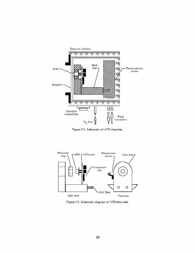
The test detector was placed on an electrical board and put inside a cooling chamber (appendix C).
The chamber was located on a three-axis translation stage for alignment purposes. A temperature con-
troller and a thermoelectric cooler (TEC) were used to fix the temperature of the APD under test. This
temperature was measured with a temperature sensor and a digital voltmeter. A stable high-voltage sup-
ply biased the APD, and a _+15-V power supply was used to bias the TIA.
The chopper controller adjusted the chopping frequency and supplied synchronization signals for
the other instruments. A personal computer sent commands to the monochromator to adjust the grating
position that sets the wavelength for the spectral scan, and it acquired the lock-in amplifier and the tem-
perature readings with a GPIB data acquisition card. Appendix B gives the model numbers, manufac-
tures, and descriptions of the instruments used in this setup.
4.2. Experimental Procedure
The reference and test detectors required accurate positioning because the output of the integrating
sphere, diffuser, and the light source have intensities that decrease by the inverse of the square of the
distance between the source and the detector. The distance between the light outlet and the detector
active area was 75 to 150 mm. A microscope with a depth of focus measured to be 200 btm was used to
position both detectors as shown in figure 9. Applying the inverted square function, the worst case devi-
ation of the intensity at the detector was _+0.53 percent. Errors due to positioning of the detectors will
cause absolute calibration uncertainty of less than 1 percent. The microscope was placed on a kinematic
mount (1 btm placement precision) so that it could be removed from the optical path and precisely
replaced in the path for detector positioning.
The monochromator was set at 690 nm, because the halogen spectral output was a maximum at this
value, and the chopping factor and measurement system range were determined for both the reference
and test detectors. The slits of the monochromator were adjusted to have a wavelength band pass of10nm.
4.3. Data Analysis and Results
The results from the measurements were analyzed with the Mathworks MATLAB software. The
MATLAB software uses vector and array processing that simplifies the analysis of large repetitive data
sets. (See appendix D.) By referring to equation (13), we can define a normalized calibration vector
{cal } given by
{_r()_)} R r A r
{cal} = {(Vr)lockin()_)} Rd Ad CF r(14)
This vector was calculated for each APD and used for converting its output voltage variation, measured
by the lock-in amplifier, into a responsivity variation with respect to wavelength.
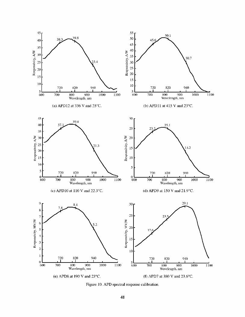
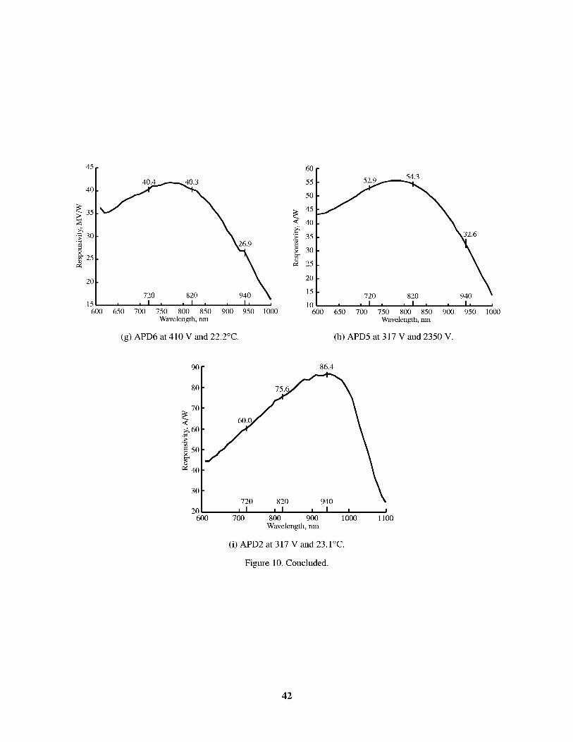
The spectral response of the test detectors is shown in figure 10. To compare the results with the
manufacturer data sheets, room temperature and manufacturer-specified bias vokage were used as indi-cated in the figure. The responsivity at wavelengths of interest to water vapor DIAL measurements are
also given. In some detectors with a built-in TIA, the value of the feedback resistance was unknown,
and the responsivity was given in V/W.
According to equation (7), the APD responsivity is directly proportional to the wavelength of the
incident light; this is true, as indicated in figure 10, for wavelengths starting at 600 nm up to the point
where the response begins to roll off. Ideally, the roll-off point would be sharp and correspond to the
energy bandgap of silicon which is 1000 nm. At this cutoff wavelength, the responsivity decreases
sharply because of insufficient energy in the incident photons for the generated electrons to overcome
the energy bandgap; this results in a reduction of the APD quantum efficiency. The deviation from the
ideal cutoff found in our characterized APD's was mainly due to charge collection inefficiency of pho-
tons outside the depletion region of the APD, which was dependent on the type and level of the dopingmaterials used to manufacture the device (refs. 10, 21, and 23).
5. Temperature Dependent Responsivity
At fixed bias voltage and wavelength, the responsivity of an APD detector increases with decreas-
ing temperature. Low temperature operation of an APD leads to an increased output signal due to the
increase in the responsivity and also a decreased noise level due to the reduction of the dark current.
This low temperature operation results in an increased signal-to-noise ratio (refs. 10, 11, 26, and 27).
This experiment investigates the effect of temperature on the APD spectral response. Empirical
relationships for the responsivity versus temperature were determined at the water vapor absorption
lines near wavelengths of 720, 820, and 940 nm. Parasitic heat load from the electronics and a nitrogen
gas purge allowed the APD operating temperature to be adjusted from near 0°C up to room temperature
(appendix C). The nitrogen gas flow was used to avoid condensation and icing inside the cooling cham-
ber. Remember that a lower operating temperature causes the detector breakdown voltage to also
decrease. Therefore, this bias must be chosen carefully while performing this test to avoid destroyingthe APD.
5.1. Experimental Procedure
The responsivity calibration setup, shown in figure 8, was used in this experiment but only for the
test detectors. During the experiment, the detector bias voltage was kept constant to ensure that the
For each APD, the following characterization results are presented:
1. The APD detector output voltage variation with wavelength {Vn(_,) }
2. The APD temperature variation with wavelength { Tn(_,) }
Ideally, the temperature should be constant with respect to wavelength. This relationship was not true in
our investigation because of some deficiencies in the temperature controller used in the experiment.
Therefore, the temperature had to be recorded for each wavelength increment {Tn(), )}. To obtain the
APD temperature Tn, this data set was averaged according to
T n = {Tn()_)} (15)
At the same temperature Tn and using equation (14), the detector output voltage variation was con-verted to a responsivity variation with respect to wavelength according to the relation
{v_0_)}
{9tn()_)} - CF n {cal} (16)
This procedure was repeated for every temperature setting giving the spectral response variation with
temperature shown in figure 11 for all APD's.
Again we used MATLAB software to analyze the results because of its ability to efficiently handle
vector and matrix operations. A responsivity vector { 9t(T)} and a temperature vector {T} were con-
stmcted, at a certain wavelength )_x, as shown in the following equations:
When applying a polynomial curve fit, the responsivity variation with temperature at )_xtook the form
M
_(T)I)_ = _ a,r,T'r' (19)m 0
10
whereM is the curve fit order and N in equation (18) is the index for maximum temperature. The
responsivity versus temperature for all APD's at the water vapor DIAL wavelengths of interest is shown
in figure 11. Table 1 gives the curve fitting results and conditions for each APD.
The responsivity with respect to the temperature relationship allowed us to determine the optimum
APD operating temperature for the future DIAL detection system. It also determined the control temper-
ature stability requirements. As an example, let us assume APD12 is the chosen detector, and it will
operate at 820 nm with 336 V and 0°C. The responsivity derivative (table 1) with respect to temperature
is given by
agl(T)aT )v 820 = -8.23 + 0.82T-23.7 x 10 3T2(20)
Thus, a temperature deviation of AT = 0.1°C, near T = 0°C, results in a responsivity deviation of
Agt =-0.823 A/W with a relative error Agt/gt = -0.72 percent. Thus, the temperature controller and
heat sinking requirements were established for the design of the final detection system.
6. Bias Voltage Dependent Responsivity
At fixed temperature and wavelength, the responsivity of an APD increases with increasing bias
voltage up to the breakdown voltage. This increase in responsivity is due to the increase of the internal
electric field leading to the transfer of more energy to the photocharge carriers, which enhances the
impact ionization process. Bias voltages above breakdown cause rapid charge carrier generation which
usually leads to device damage if applied for long periods of time (refs. 21, 23, and 24). This experiment
investigates the effect of the APD bias voltage variation on the spectral response of interest and obtains
responsivity versus bias voltage relations at the water vapor DIAL wavelengths.
6.1. Experimental Procedure
Similar to the previous experiment, the responsivity calibration setup was used only for the test
APD's. During the experiment, the APD temperature was kept constant at room temperature to ensure
that the spectral response variation is only due to the bias voltage. The detector position with respect to
the light source was adjusted to the same value as for the responsivity calibration experiment to ensure
the same light intensity input.
With the high-voltage supply shown in figure 8, the detector bias is set to a certain value, and the
temperature was stabilized by the controller to room temperature. The output peak-to-peak voltage was
then measured with the oscilloscope, and its rms value was measured with the lock-in amplifier in order
to calculate the chopping factor. Next, the wavelength was scanned from 600 to 1100 nm with a step
increment of 10 nm. For each step increment, the wavelength, output voltage, and temperature were
recorded with the computer. Finally, the experiment was repeated for a set of different bias voltages.
This procedure was repeated for each APD under investigation.
6.2. Data Analysis and Results
At the end of this experiment, each APD had a group of data files describing its output voltage vari-
ation with wavelength at a given bias voltage. The data analysis was performed once again by using
MATLAB software. The value of the bias voltage VBn was measured directly from the high-voltagesupply. For a certain APD at a given bias voltage, the available data were as follows:
By using a polynomial curve fit, the responsivity variation with bias voltage is given by
M
N(V)I;% = Z art,Vrr' (23)m 0
where M is the curve fit order and N is the index for maximum voltage bias. This analysis was applied to
each APD at wavelengths of 720, 820, and 940 nm.
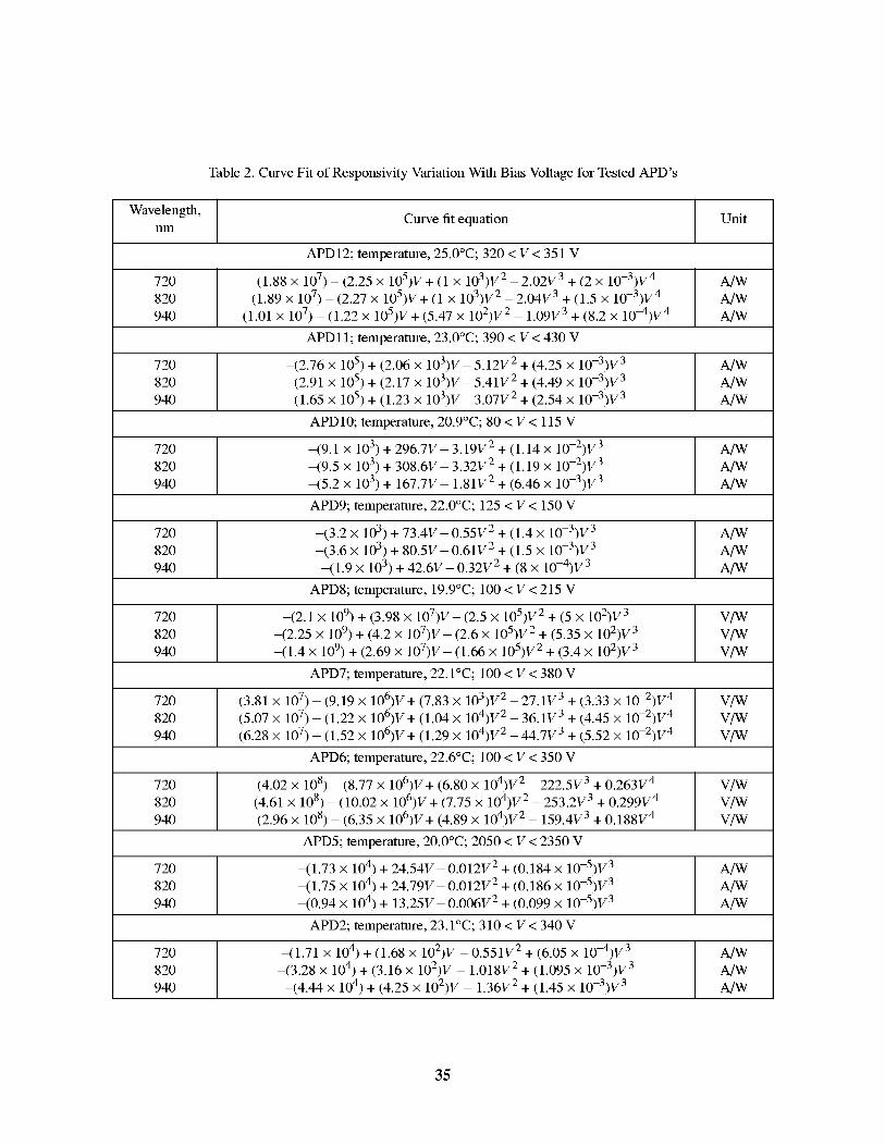
The experimental results are shown in figure 12. For each detector, the spectral response variation
with bias voltage is shown on the set of curves to the left, and the responsivity variation with bias
voltage is shown to the right. Table 2 shows the curve fit coefficients and the test conditions for eachdetector.
The responsivity-bias voltage relation can be used for determining the APD operating bias in the
final DIAL detection system, and it gives an error estimate which helps in evaluating the system accu-
racy. As an example, assume APD12 is the chosen detector, and it operates at 820 nm with a bias volt-
age of 336 V and a temperature of 25°C. When referring to figure 12(b), we find that any small variation
in the bias voltage around 336 V will cause a small variation in its responsivity relative to higher voltage
bias, but the value of the responsivity is relatively stable. On the other hand, table 2 shows that the
responsivity derivative with respect to bias voltage is given by
0N(V) = -2.27 x 10⁵ + 2 x 10³V - 6.12V 2 + 6 x 10 3V33V 820
(24)
Thus, a bias voltage deviation of AV = 1 V near the bias of 336 V bias results in a responsivity deviation
of An = 1.8034 A/W which will lead to a relative error of AN/N = 4 percent.
12
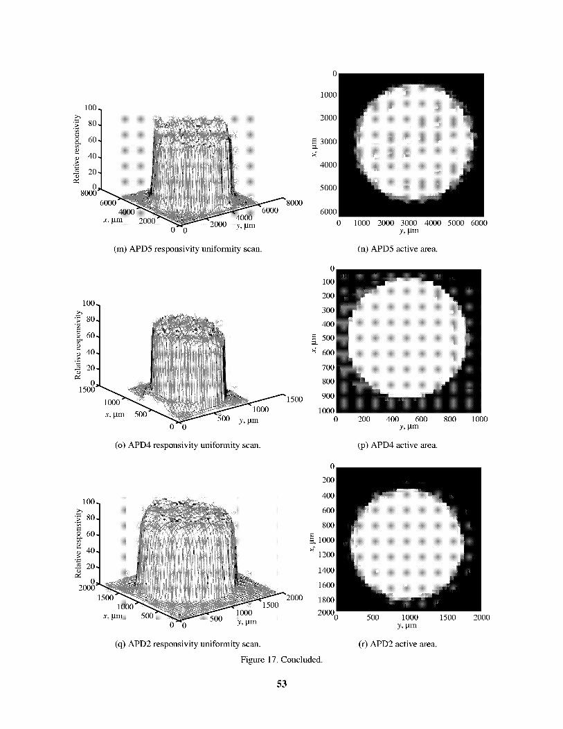
7. Responsivity Uniformity Scan
The APD sensitive area can be considered a group of point detectors distributed along the surface.
Ideally, this distribution is uniform with each of these detectors having the same responsivity for similaroperating conditions, and therefore, the responsivity distribution is constant along the APD surface.
Practically, this condition is not true because of defects developed in the APD manufacturing processes.
In this experiment, we investigated the uniformity of APD responsivity across its surface and deter-
mined its active area. This measurement required a relatively small-spot-size light source and the ability
to scan it across the detector area. Measuring the APD output voltage as a function of light spot position
results in a responsivity map of the APD area.
7.1. Experimental Setup and Procedure
The small-spot-size light source was achieved with the setup shown in figure 13. A 633-nm He:Ne
laser output was focused by using a microscope objective. The position of the detector was adjusted
with a computer-controlled two-dimensional translation stage. The motion of the detector was adjusted
so that the focused laser beam spot and the APD sensitive area remained in the same plane. A neutral
density filter was used to avoid APD saturation.
The laser focusing optical system was calibrated to determine the displacement between the laser
focus at its minimum waist and the visual focus of the microscope system shown in figure 14. In order
to obtain this calibration, a pinhole was mounted on a three-dimensional translation stage, as shown in
figure 15. The laser focus was determined by positioning the pinhole such that the maximum laser out-
put was observed on the detector. The laser focus was measured with the micrometer on the translation
stage. The visual focus was determined by viewing the best focus of the pinhole through the eyepiece.
The test detectors were positioned by finding the visual focus of the detector surface and then translat-
ing to the laser focus by the calibrated displacement described previously. During the scan sequence the
detector moves in a two-dimensional raster scanning sequence with a fixed step size. The data are then
plotted and analyzed with MATLAB.
7.2. Data Analysis and Results
The focused laser spot intensity profile was characterized by scanning a 10-gm-diameter hole in the
plane of the laser focus. The results of this scan are displayed in figure 16, and the full width half maxi-
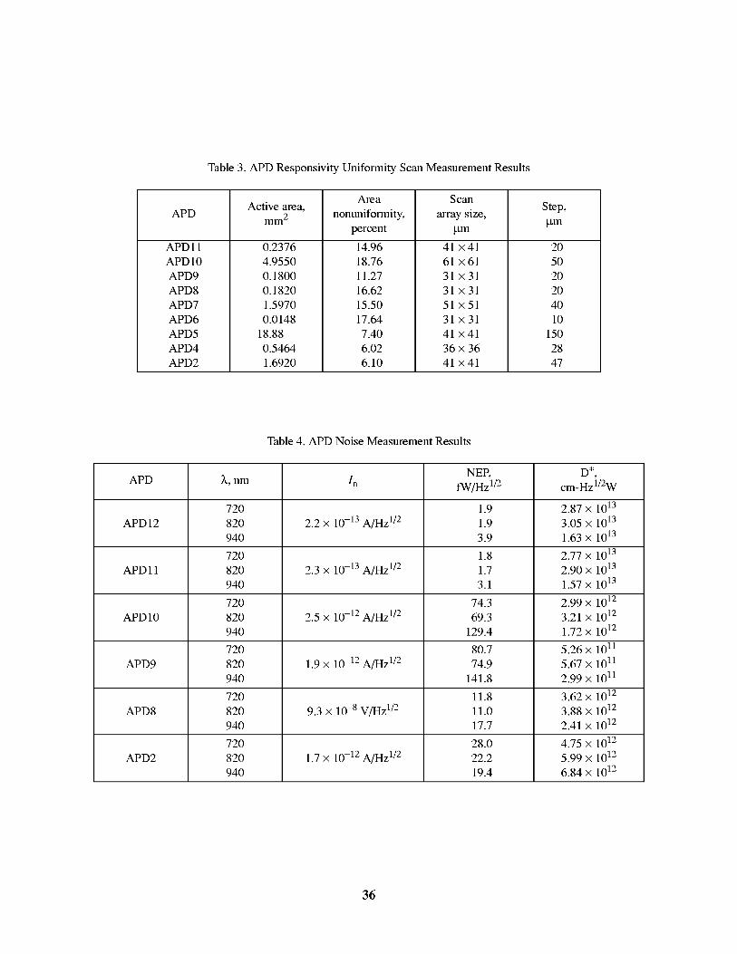
mum (FWHM) of the laser spot was 8 gm. Table 3 lists the results of each APD active area, percentage
nonuniformity, scanned array step format, and the step size. The active area was defined by the FWHM
points in the uniformity scans. The nonuniformity is defined by
StdNonuniformity - Mean 100 (25)
where Std and Mean are the standard deviation and the mean of the surface scan data, respectively.
The normalized surface scan results for the tested APD's (three-dimensional plots shown to the left)
and the surface images (shown to the right) are shown in figure 17. In the surface images, darker areas
represent lower responsivity, whereas brighter areas represent higher responsivity.
Noise signals can be divided into two kinds: systematic noise and natural device noise. Systematic
noise is mainly due to conduction and interference from the wiring associated with the detector and the
surrounding instruments (such as power supplies and pulse generators), and it is independent of the
detection process. It can be successfully reduced by proper shielding of the connecting wires, ground-
ing, differential measurement technique, or measuring it in dark condition and subtracting it from the
detector output with light applied. The natural device noise is fundamental in nature and is mainly due
to the operation of the optical detector itself. It is due to random processes and, thus, can be reduced by
averaging. The dominant types of natural device noise are the signal-induced shot noise, the dark
current shot noise, and the Johnson noise. In this section, we will discuss these dominant natural noise
sources associated with APD operation and its TIA circuit and how it can be measured (refs. 10, 11,
and 21).
8.1. Types of APD Inherent Noise
The first type of APD inherent noise is signal-induced shot noise. It is generated by the randomness
in photon arrival times which leads to fluctuations in the detector output signal. Because of the internal
gain in the APD, an additional noise is added to the optical shot noise; this is known as the multiplica-
tion gain noise, which is mainly due to the randomness in the impact ionization process. The total shot
noise current in this case is given by (refs. 10, 11, 12, 28, and 29)
. 2 = P_,On)shot 2qq2BG2 hc (26)
where B is the effective bandwidth of the detector and G is the device internal gain.
The second type of APD noise is the dark current shot noise. The APD dark current is given by the
first term in equation (4) which contributes a dc offset to the detected current signal. This dc offset can
be reduced by proper filtering or by adding another offset with opposite polarity. The problem with dark
current lies in the shot noise it creates which is independent of the operating frequency. The dark currentnoise can be obtained from (refs. 10, 11, and 12)
. 2(/n)dark = 2qidarkGB (27)
14
Thenoisesourcesdescribedaboveareindependent;thereforethenoisepowerscanbeaddedtogether.TheresultingequivalentnoisecurrentI n of the APD is given by combining the noise currents
of each noise source obtained from equations (26) and (27) as
_. 2 . 2I n = (/n)shot + (/n)dark (28)
and the signal-to-noise ratio is given by
2S Id
N 12n
(29)
The noise and signal as a function of the input optical power are shown in figure 18. Only the optical
shot noise depends on the input power. The power independent noise is plotted as a straight horizontal
line and represents the dark current. The photon shot noise increases as the square root of the optical
power. This shot noise power term adds directly to the other noise power of the system. The signal cur-
rent increases linearly with input power as shown in figure 18. The power at which the signal current
equals the total noise current is called the noise equivalent power (NEP), which is the minimum power
required to achieve a unity signal-to-noise ratio used to define the detector minimum detectable signal.The NEP (in W/Hz 1/2) can be evaluated from
I n
NEe = - (30)9¢
where In is the noise current spectral density in A/Hz 1/2 and _Rin A/W. Another figure of merit useful incomparing APD's in terms of noise is called the detectivity D* (in cm-Hzl/2/W). This figure of merit is
independent of the detector area A and is given by
D*- ff_ (31)NEP
An additional noise source introduced to the APD output photocurrent is due to the current-to-
voltage conversion process of the TIA. The operational amplifier noise at its output may be considered a
combination of the effects of several independent noise sources at its input as shown in figure 19.
The first noise source is the amplifier equivalent noise voltage generator with spectral density
e v (V/Hzl/2). The second noise source is the noise voltage generated by the amplifier input current noise
flowing through the feedback resistor ei (V/Hzl/2). Usually values for these two noise sources are given
in the amplifier data sheet. The last noise source is the Johnson noise er (in V/Hz 1/2) due to the feedback
resistance Rf and is given by
(32)
where kB is Boltzmann constant and T is the temperature in Kelvins. The total noise at the amplifier out-put is then given by the sum of the individual noise powers plus the APD noise itself as shown in the
following equation (ref. 25):
_/2 2 2 2E n = ev+e i +e r+(InR f) (33)
15
8.2. APD Noise Measurement and Results
The APD noise measurements were performed by using a spectrum analyzer with a 1-Hz normal-
ized spectrum at a spectral resolution bandwidth of 10 kHz. Appropriate care was taken to ensure that
the detector dark current and preamplifier noise were the dominant noise sources. The measured power
spectral noise n (in dBm) was converted to the APD noise current spectral density In by the equation
Io0"lnRL x 10 3(34)
where R L is the APD load resistance and G A is a preamplifier gain. This quantity was observed to beconstant over the APD bias vokage and temperature operating range. Table 4 gives the noise current
spectral density, NEP, and D* for the tested detectors at their responsivity calibration bias voltage and
temperature.
The results of this experiment are very important since they directly indicated that APD12 and
APD11 were the best detectors for the water vapor DIAL detection system; APD2 represents the detec-
tor that is currently used in the LASE detection system.
The APD excess noise factor F as a function of its gain G and ionization ratio _; is given by
(refs. 29, 30, and 31)
F = _¢G+(1-_¢)(2 -1) (35)
For SLIK APD's, APD12 and APD11, the gain is in the range of 500, whereas for a reach-through
structure, such as APD2, the gain is 150. Substituting the gain and the ionization factor values given in
section 1.2, we find that the SLIK structure has a 40-percent reduction in the excess noise factor over
the reach-through structure. A quick comparison (table 4) agrees with this statement and indicates the
lower noise content of APD12 and APD11, which helps in achieving our goal of increasing the signal-
to-noise ratio of the DIAL detection system by a factor of 10 over the current detection system (APD2).
9. Frequency Response
The frequency response of an APD is determined by the device time response. The time response of
an APD is the time interval between the event of photon absorption and the event of photocurrent gener-
ation at its output. This time is dependent on the transient time spread, the diffusion time, the RC time
constant, and the avalanche buildup time.
Transient time spread is the time interval between photocharge carrier generation and its detection.
The charge delivered to the external circuit, contributing to the photocurrent, by carrier motion in the
APD material is not provided instantaneously but consumes a time interval because of the drift of the
carrier. This time interval is known as the transient time spread. Since holes are much slower than
electrons, the transient time spread is dominated by the hole mobility.
Carriers generated outside the depletion region, but sufficiently close to it, take time to diffuse into
it. These carriers will contribute to the photocurrent. But since the diffusion is a slow process relative to
These characterization experiments provided the basis for the design of an advanced 14-bit atmo-
spheric water vapor detection system, with the APD and its operating parameters indicated in the above
table. These detectors represent the best available APD's for the near infrared detection of atmospheric
water vapor even with their smaller sensitive area.
19
Appendix A
APD Manufacturer's Data
The manufacturer's data for the APD's investigated are given in the following table.
20
I,_ _,-_ _ _ _ {'q _ _ _ {'q
{'q X X _ _ _ _
N N _ N N _
_ {'q _ {'q {-q {'q
{.q {'q {'q
i
_ _ _ _ _ _ _._
21
Appendix B
Characterization Instruments
The reference detector was an ORIEL K7034 detector. It was a p-i-n diode, with a sensitive area of100 mm 2. The TIA feedback resistor associated with the detector was set to 106 £2. Figure B1 gives the
detector spectral response which was used to calibrate all the test APD's.
The test instruments were as follows:
Light source: ORIEL 66181
Optical chopper: ORIEL 75152
Integrating sphere: ORIEL 70451
Temperature controller: Amherst Scientific 7600
High voltage supply: Stanford Research System PS350
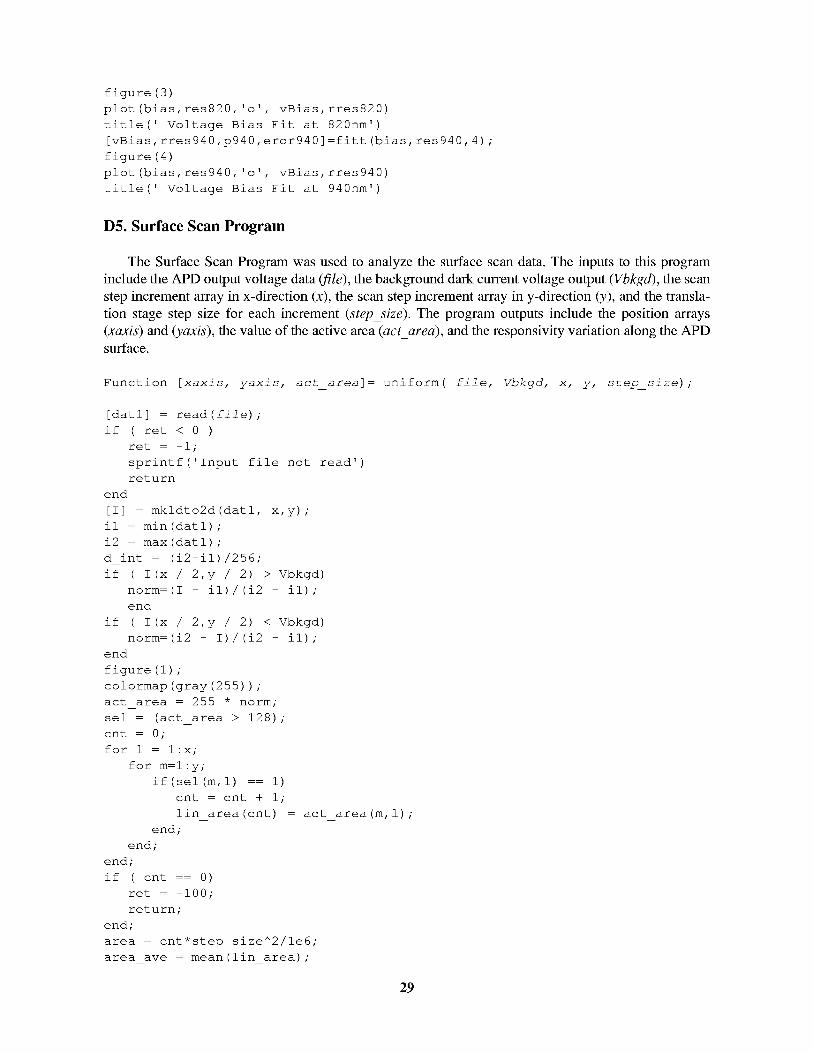
The Surface Scan Program was used to analyze the surface scan data. The inputs to this program
include the APD output voltage data _le), the background dark current voltage output (Vbkgd), the scan
step increment array in x-direction (x), the scan step increment array in y-direction (y), and the transla-
tion stage step size for each increment (step_size). The program outputs include the position arrays
(xaxis) and (yaxis), the value of the active area (act_area), and the responsivity variation along the APDsurface.
Function [xaxis, yaxis, act_area] = uniform( file, Vbkgd, x, y, step_size) ;
[datl] = read(file) ;
if ( ret < 0 )
ret = -i ;
sprintf('Input file not
return
end
[I] = mkldtold(datl, x,y) ;
il = min(datl) ;
i2 = max (datl) ;
d int = (il-il)
if ( I (x / 2,y
norm = (I - il
end
if ( I (x / 2,y
norm = (i2 - I
end
figure(1) ;
colormap (gray (255) ) ;
act area = 255 * norm;
sel = (act area > 128);
cnt = 0 ;
for 1 = 1 :x;
for m=l :y;
if(sel (re,l) == i)
cnt = cnt + i;
lin area(cnt) = act
end;
end;
end;
if ( cnt == 0)
ret = -i00;
return;
end;
area = cnt*step_size^2/le6;
area ave = mean(lin area);
256;
2) > Vbkgd)
/ (i2 - il) ;
2) < Vbkgd)
/ (i2 - il) ;
read')
area (m, i) ;
29
area std = std(lin area);
per_area : area_std*100/area_ave;
xaxis : step_size* (l:x) ;
yaxis : step_size* (l:y) ;
v : act area*d int+il;
maxv : max (max(v)) ;
minv: rain(rain(v)) ;
for I : 1 :x;
for j = 1 :y;
v(i, j) = v(i, j)-minv;
v(i, j) : (i00/ (maxv-minv))*v(i, j) ;
end
end
mesh (xaxis, yaxis, v) ;
title( [file, ' : Active Area Response
Percent ' ] ) ;
zlabel ('Relative Responsivity') ;
xlabel ('Y-Position in microns') ;
ylabel ('X-Position in microns') ;
colormap ( 'default ' ) ;
CM : colormap;
TiffFile = 'name num.ext';
TiffFile : strrep( TiffFile, 'name', file);
TiffFile : strrep( TiffFile, 'num', 'i');
TiffFile = strrep( TiffFile, 'ext', 'tif');
figure (2) ;
colormap (gray (255) ) ;
u = act area;
maxu : max (max(u)) ;
minu : rain(rain(u)) ;
image (xaxis, yaxis, u) ;
title( [file, ' : Active Area ',
xlabel ('Y-Position in microns') ;
ylabel ('X-Position in microns') ;
CM : colormap;
axis ( 'square ' ) ;
TiffFile = 'name num.ext';
TiffFile : strrep( TiffFile, 'name', file);
TiffFile : strrep( TiffFile, 'num', '2');
TiffFile = strrep( TiffFile, 'ext', 'tif');
Uniformity ' num2str(per area), ' STD
num2str(area), ' mm^2']);
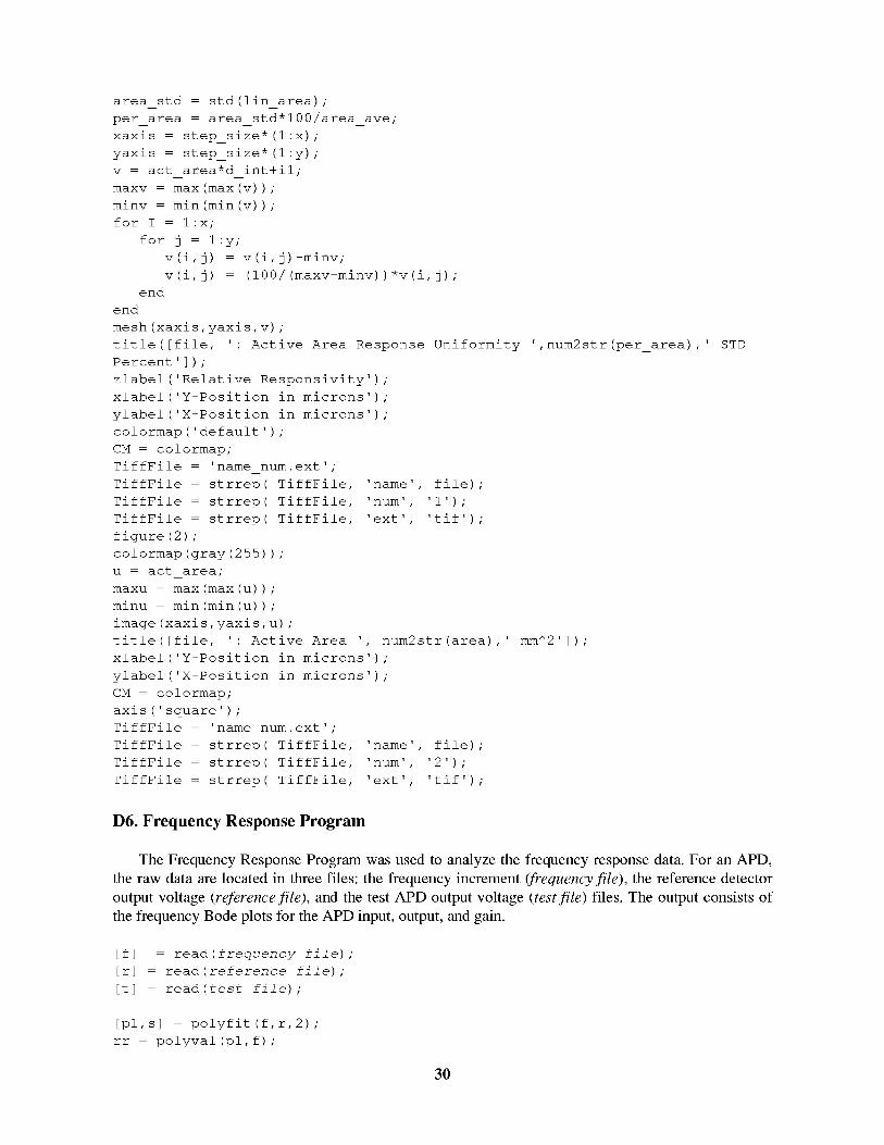
D6. Frequency Response Program
The Frequency Response Program was used to analyze the frequency response data. For an APD,
the raw data are located in three files: the frequency increment (frequency file), the reference detectoroutput voltage (reference file), and the test APD output voltage (test file) files. The output consists of
the frequency Bode plots for the APD input, output, and gain.
[f]
[r]
[t]
= read (frequency file) ;
= read(reference file);
= read(test file ;
[pl,s] = polyfit (f,r 2) ;
rr = polyval (pl, f) ;
30
figure (1 )
semilogx (f, r, 'o', f, rr)
grid
xlabel('Frequency in Hz')
ylabel ('Input in dB')
[p2,s] = polyfit (f,t,2),
tt = polyval (p2, f) ;
figure (2)
semilogx (f, t, 'o',f, tt)
grid
xlabel ('Frequency in Hz')
ylabel ('Output in dB')
for I = 1:35;
g(I) = t (I)-r(I) ;
end
g=g';
figure (3 )
[p3,s] = polyfit (f,g,2)
gg = polyval (p3, f) ;
semilogx (f, g, 'o ' , f, gg)
grid
xlabel ('Frequency in Hz')
ylabel ('Gain in dB')
31
References
1. Christopherson, Robert W.: Geosystems: An Introduction to Physical Geography. Maxwell Macmillan Int.,1992.
2.
3.
4.
Starr, D. O'C.; and Melfi, S. H., eds.: The Role of Water Vapor in Climate A Strategic Research Plan for the
Proposed GEWEX Water Vapor Project (GVaP). NASA CP-3120, 1991.
Zhang, Z.; and Krishnamurti, T. N.: Ensemble Forecasting of Hurricanes Tracks. Bull. Am. Meteorol. Soc.,
1997, pp. 2785-2695,
Measures, Raymond M.: Laser Remote Sensing: Fundamentals and Applications. John Wiley & Sons, Inc.,1984.
5.
.
Whiteman, D. N.; Melfi, S. H.; and Ferrare, R. A.: Raman Lidar System for the Measurement of Water Vapor
and Aerosols in the Earth's Atmosphere. Appl. Opt., vol. 31, no. 16, June 1992, pp. 3068-3082.
Grant, William B.: Differential Absorption and Raman Lidar for Water Vapor Profile Measurements: A
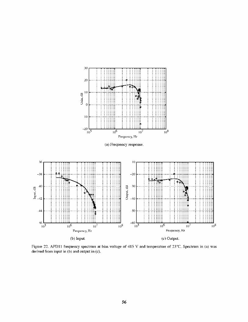
Figure 22. APDll frequency spectrum at bias voltage of 415 V and temperature of 23°C. Spectrum in (a) was
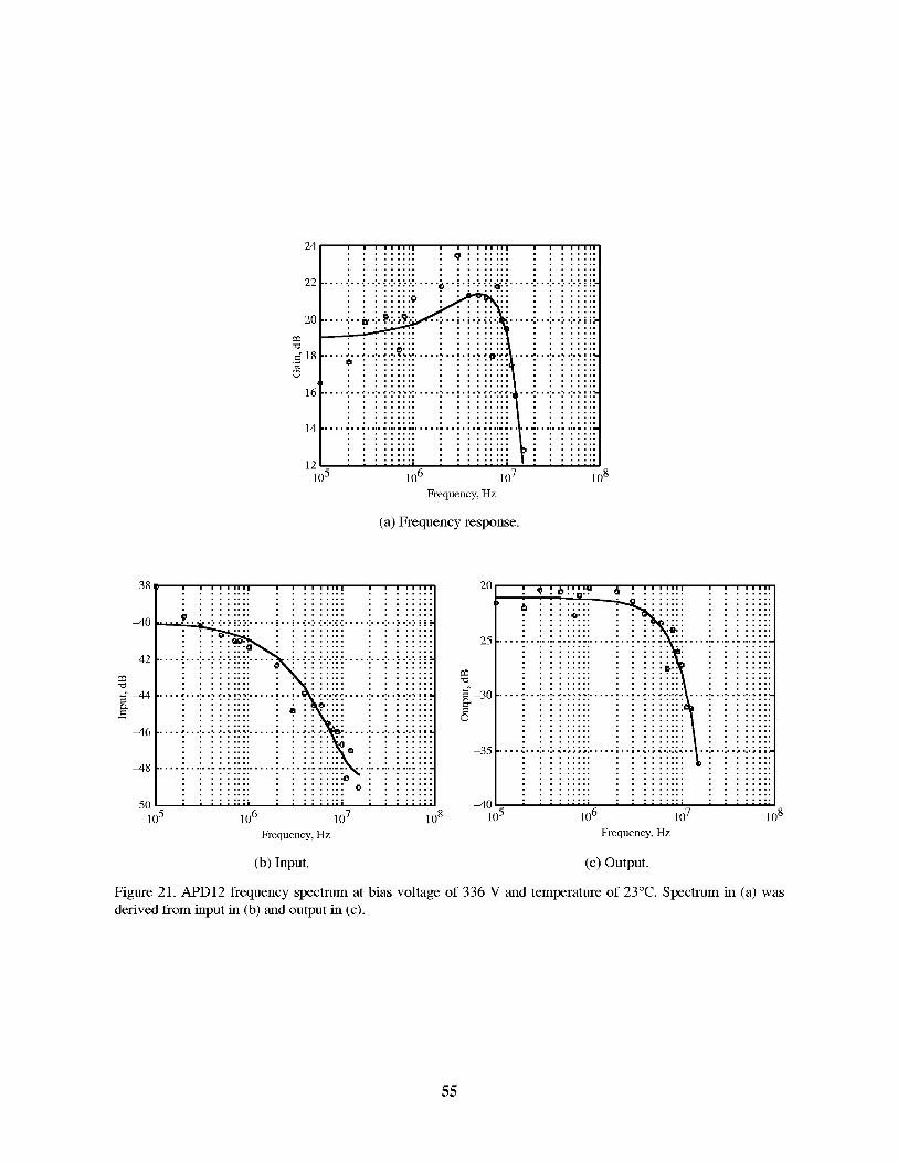
derived from input in (b) and output in (c).
56
Form ApprovedREPORT DOCUMENTATION PAGE OMBNo.0704-0188
Public reporting burden for this collection of information is estimated to average 1 hour per response, including the time for reviewing instructions, searching existing data sources,gathering and maintaining the data needed, and completing and reviewing the collection of information. Send comments regarding this burden estimate or any other aspect of thiscollection of information, including suggestions for reducing this burden, to Washington Headquarters Services, Directorate for Information Operations and Reports, 1215 JeffersonDavis Highway, Suite 1204, Arlington, VA 22202-4302, and to the Office of Management and Budget, Paperwork Reduction Project (0704-0188), Washington, DC 20503.
1. AGENCY USE ONLY (Leave blank ]2. REPORT DATE 3. REPORTTYPE AND DATES COVERED
I July 2000 Technical Publication4. TITLE AND SUBTITLE 5. FUNDING NUMBERS
Characterization of Advanced Avalanche Photodiodes for Water Vapor LidarReceivers WU 622-63-13-70
6. AUTHOR(S)
Tamer F. Refaat, Gary E. Halama, and Russell J. DeYoung
7. PERFORMING ORGANIZATION NAME(S) AND ADDRESS(ES)
NASA Langley Research CenterHampton, VA 23681-2199
9. SPONSORING/MONITORING AGENCY NAME(S) AND ADDRESS(ES)
National Aeronautics and Space AdministrationWashington, DC 20546-0001
8. PERFORMING ORGANIZATION
REPORT NUMBER
L-17936
10. SPONSORING/MONITORING
AGENCY REPORT NUMBER
NASA/TP-2000-210096
11. SUPPLEMENTARY NOTES
Refaat: Old Dominion University, Norfolk, VA; Halama and DeYoung: Langley Research Center, Hampton, VA.
12a. DISTRIBUTION/AVAILABILITY STATEMENT
Unclassified-Unlimited
Subject Category 33 Distribution: StandardAvailability: NASA CASI (301) 621-0390
12b. DISTRIBUTION CODE
13. ABSTRACT (Maximum 200 words)
Development of advanced differential absorption lidar (DIAL) receivers is very important to increase the accuracyof atmospheric water vapor measurements. A major component of such receivers is the optical detector. In the near-infrared wavelength range avalanche photodiodes (APD's) are the best choice for higher signal-to-noise ratiowhere there are many water vapor absorption lines. In this study, characterization experiments were performed toevaluate a group of silicon-based APD's. The APD's have different structures representative of different manufac-turers. The experiments include setups to calibrate these devices, as well as characterization of the effects ofvoltage bias and temperature on the responsivity, surface scans, noise measurements, and frequency responsemeasurements. For each experiment, the setup, procedure, data analysis, and results are given and discussed. Thisresearch was done to choose a suitable APD detector for the development of an advanced atmospheric water vapordifferential absorption lidar detection system operating either at 720, 820, or 940 nm. The results point out thebenefits of using the super low ionization ratio (SLIK) structure APD for its lower noise-equivalent power, which
1/2was found to be on the order of 2 to 4 fW/Hz , with an appropriate optical system and electronics. The watervapor detection systems signal-to-noise ratio will increase by a factor of 10.
14. SUBJECT TERMS
APD; Reach-through structure; SLIK structure; Beveled-edge structure15. NUMBER OF PAGES