Page 1
Graduate Theses, Dissertations, and Problem Reports
2015
Characterization of Defects on MOCVD Grown Gallium Nitride Characterization of Defects on MOCVD Grown Gallium Nitride
Using Transient Analysis Techniques Using Transient Analysis Techniques
Sujan Phani Kumar Kasani
Follow this and additional works at: https://researchrepository.wvu.edu/etd
Recommended Citation Recommended Citation Kasani, Sujan Phani Kumar, "Characterization of Defects on MOCVD Grown Gallium Nitride Using Transient Analysis Techniques" (2015). Graduate Theses, Dissertations, and Problem Reports. 7100. https://researchrepository.wvu.edu/etd/7100
This Thesis is protected by copyright and/or related rights. It has been brought to you by the The Research Repository @ WVU with permission from the rights-holder(s). You are free to use this Thesis in any way that is permitted by the copyright and related rights legislation that applies to your use. For other uses you must obtain permission from the rights-holder(s) directly, unless additional rights are indicated by a Creative Commons license in the record and/ or on the work itself. This Thesis has been accepted for inclusion in WVU Graduate Theses, Dissertations, and Problem Reports collection by an authorized administrator of The Research Repository @ WVU. For more information, please contact [email protected] .
Page 2
Characterization of Defects on MOCVD Grown Gallium Nitride
Using Transient Analysis Techniques
Sujan Phani Kumar Kasani
Thesis submitted to the
Benjamin M. Statler College of Engineering and Mineral Resources
at West Virginia University
in partial fulfillment of the requirements for the degree of
Master of Science
in
Electrical Engineering
Lawrence A. Hornak, Ph.D., Chair
Dimitris Korakakis, Ph.D.
Jeremy Dawson, Ph.D.
Ayyakkannu Manivannan, Ph.D.
Lane Department of Computer Science and Electrical Engineering
Morgantown, West Virginia
2015
Keywords: Traps, Energy Levels, Capacitance transient, Schottky diode
Copyright 2015 Sujan Kasani
Page 3
ABSTRACT
CHARACTERIZATION OF DEFECTS ON MOCVD GROWN GALLIUM NITRIDE
USING TRANSIENT ANALYSIS TECHNIQUES
Sujan Phani Kumar Kasani
Since the invention of the first visible spectrum (red) LED by Holonyak in 1962, there has been a
need for more efficient, more reliable and less expensive LEDs. The III-nitrides revolutionized
semiconductor technology with their applications in the blue LED’s. However the internal
quantum efficiency of LED’s are limited by the deep level traps in GaN substrate. Traps are
defects in the crystal lattice, which depends on growth parameters. These traps act as non-
radiative centers where non-radiative recombination occurs without conversion of available
energy into light. Characterization of these traps in a material is necessary for better
understanding of the material growth quality and resulting device performance. In this work
Capacitance-Voltage (C-V) and Deep Level Transient Spectroscopy (DLTS) are conducted
which provide electronic properties of trap centers like activation energy, doping concentration
and capture cross-section. In n-GaN grown by Metalorganic Chemical Vapor Deposition
(MOCVD) on Sapphire two defects types are detected and are characterized by Capacitance-
Voltage and Deep Level Transient Spectroscopy. Two deep levels E1 and E2 are typically
observed in n-GaN with the activation energies of 0.21eV and 0.53eV at 125°K and 325°K,
respectively. The deep level E1 is caused by linear line defects along dislocation cores while
deep level E2 is related to point defects. The characterization techniques, experimental systems
and preliminary characterization results are discussed in detail.
Page 4
ACKNOWLEDGEMENTS
It’s my pleasure, to thank all the people involved in my thesis.
I would like to express my deepest gratitude to my advisor Dr. Hornak, for his invaluable
assistance, support and encouragement throughout my research. This thesis would not have been
possible without his intellectual support and the resources he made available to me.
I am thankful to my committee members, Dr. Korakakis, Dr. Dawson and Dr. Manivannan for
their encouragement, technical discussions and feedback.
I sincerely acknowledge Dr. Kolin Brown for his support in the cleanroom. Immense thanks to
my labmates Anand Kadiyala, Lekha Kuchipudi, Joshua Justice, Vishal Narang, Gadde Akshitha
and Vamsi Kumbham for their help and knowledge exchange.
I owe my sincere thanks and dedicate this thesis to my parents Mr. K.V. Ramana Rao (M.A.),
Mrs.K.Padhma Latha (M.A.), my sister K. Naga Pavani (M.Sc.) and my girlfriend V.Sarika
(M.S) whose love and sacrifice for me is beyond anything I will ever understand.
Special thanks to my friends N. Athul Madhur, P. Surekha, Rinjumon C. Abhraham, N. Dileep,
K. Shiva, B. Sri Divya and my Friendship is Ocean group mates.
Page 5
iv
Table of Contents Chapter 1: Introduction ................................................................................................................................ 1
1.1 Overview ............................................................................................................................................. 1
1.2 Effects of traps in p-n junction ............................................................................................................ 2
1.3 Defect characterizing techniques ....................................................................................................... 3
1.3.1 DLTS (Deep Level Transient Spectroscopy): .............................................................................. 4
1.3.2 C-V (Capacitance – Voltage): ...................................................................................................... 4
1.3.3 Hall Effect .................................................................................................................................... 4
Chapter 2: Literature Review ........................................................................................................................ 6
2.1 Overview: ............................................................................................................................................ 6
2.2 Gallium Nitride (GaN) .......................................................................................................................... 6
2.3 Growth of GaN on MOCVD: ................................................................................................................ 8
2.4 Traps .................................................................................................................................................... 8
2.4.1Classification of defects ................................................................................................................ 9
2.5 Charging and Discharging of Traps in space charge region .............................................................. 11
Chapter 3: DEEP LEVEL TRANSIENT SPECTROSCOPY OF GaN ..................................................................... 14
3.1 Overview ........................................................................................................................................... 14
3.2 Capacitance – Voltage (CV) measurements ...................................................................................... 14
3.2.1 Schottky diodes in n-type GaN .................................................................................................. 17
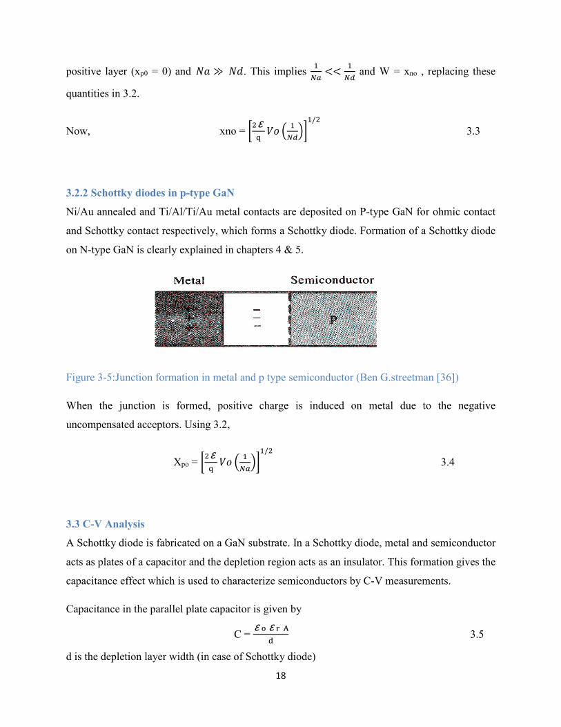
3.2.2 Schottky diodes in p-type GaN .................................................................................................. 18
3.3 C-V Analysis ....................................................................................................................................... 18
3.4 Deep Level Transient Spectroscopy (DLTS) ....................................................................................... 20
Chapter 4: Metal Contacts on GaN ............................................................................................................. 23
4.1 Schottky Contact ............................................................................................................................... 23
4.1.1 Schottky contact on n-type ......................................................................................................... 23
4.1.2 Schottky contact on p-type ......................................................................................................... 25
4.1.3 Forward and reverse bias characteristics of Schottky contacts ................................................. 27
4.2 Ohmic Contacts ................................................................................................................................. 29
4.2.1 Ohmic contacts on n-type GaN .................................................................................................. 29
4.2.2 Ohmic contacts on p-type GaN .................................................................................................. 30
Page 6
v
4.3 Conduction mechanisms in metal-semiconductor contacts ............................................................. 31
Chapter 5: Schottky Diode fabrication ........................................................................................................ 34
5.1 Sample Annealing ............................................................................................................................. 34
5.2 Surface cleaning ................................................................................................................................ 35
5.3 Photolithography .............................................................................................................................. 36
5.3.1 Spinning:..................................................................................................................................... 37
5.3.2 Soft bake: ................................................................................................................................... 37
5.3.3 Mask Alignment and Exposure .................................................................................................. 37
5.3.4 Hard bake or post exposure bake .............................................................................................. 39
5.3.5 Flood Exposure: .......................................................................................................................... 39
5.4 Development ..................................................................................................................................... 40
5.5 Metal Deposition .............................................................................................................................. 40
5.6 Lift Off ............................................................................................................................................... 41
5.7 Contacts Annealing ........................................................................................................................... 42
Chapter 6: DLTS Setup and DLTS Study of GaN .......................................................................................... 45
6.1Overview ............................................................................................................................................ 45
6.2 DLTS Hardware: ................................................................................................................................. 45
6.2.1 Refrigerator system: ................................................................................................................... 45
6.2.2 Temperature Controller .............................................................................................................. 46
6.2.3 Pulse Signal generator ................................................................................................................ 46
6.2.4 Capacitance meter ...................................................................................................................... 46
6.2.5 Oscilloscope ............................................................................................................................... 46
6.2.6 Package and connectors: ............................................................................................................ 47
6.3 Experimental Work ........................................................................................................................... 47
6.3.1 Schottky diode on GaN .............................................................................................................. 47
6.3.2 CV study on GaN ........................................................................................................................ 47
i. CV analysis on n-GaN: ................................................................................................................. 48
ii. CV analysis on p-GaN: ................................................................................................................. 49
6.3.3 DLTS study on GaN ......................................................................................................................... 50
Conclusion and Future Work .................................................................................................................. 53
References .................................................................................................................................................. 54
Page 7
vi
List of Figures
Figure 1.1: a) Recombination without traps b) Recombination with traps .................................................. 2
Figure 1.2: Hall effect on n-type device [38] ................................................................................................ 5
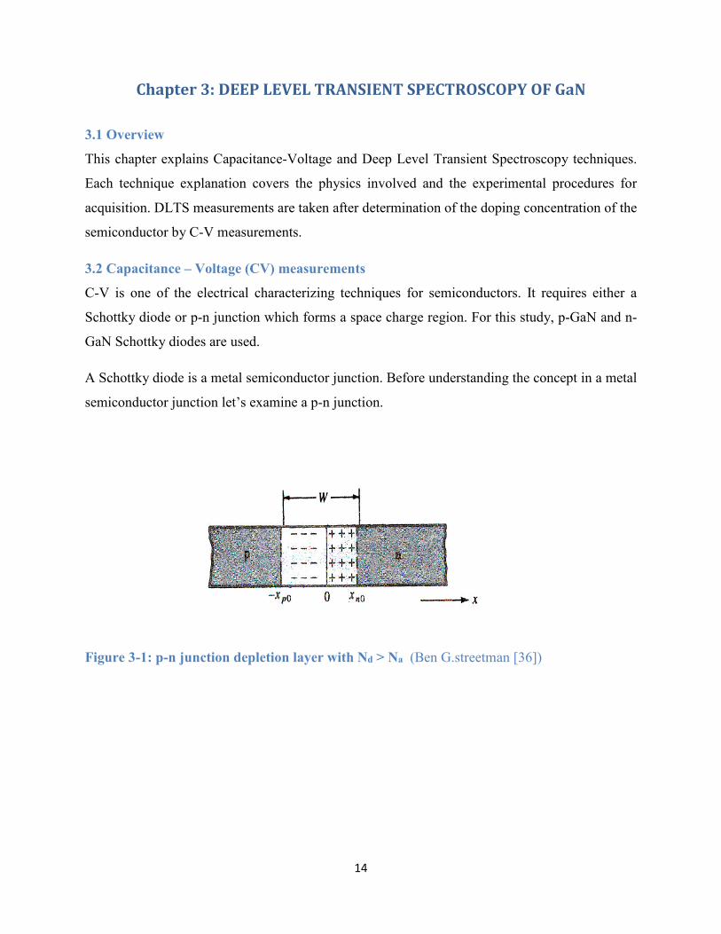
Figure 3-1: p-n junction depletion layer with Nd > Na (Ben G.streetman [36]) ......................................... 14
Figure 3-2: charge density with in depletion region neglecting free carriers (Ben G.Streetman [36]) ....... 15
Figure 3-3: a) Metal semiconductor before contact b) Metal semiconductor after contact (Gísli Jóhann
Grétarsson[31]) ........................................................................................................................................... 17
Figure 3-4: Junction formation in metal and n type semiconductor (Ben G.streetman [36]) ..................... 17
Figure 3-5:Junction formation in metal and p type semiconductor (Ben G.streetman [36]) ...................... 18
Figure 4-1: Energy band diagram of metal and n-type semiconductor (Øm > Øs ) a) before contact b) just
in contact c) thermal equilibrium (B. Van Zeghbroeck, 2011) [59] ........................................................... 24
Figure 4-2: Current Voltage characteristics of Schottky contact on n-type GaN ....................................... 25
Figure 4-3:Energy band diagram of metal and p-type semiconductor a) before b) just in contact c) thermal
equilibrium (B. Van Zeghbroeck, 2011)[59] .............................................................................................. 26
Figure 4-4: Current Voltage characteristics of Schottky contact on p-type GaN ....................................... 26
Figure 4-5: Energy band diagram of metal semiconductor in forward bias [67] ........................................ 27
Figure 4-6: Energy band diagram of metal semiconductor in reverse bias [67] ......................................... 27
Figure 4-7: Typical current-voltage characteristics of Schottky diode (Ben G.streetman[68]) .................. 28
Figure 4-8: Current Voltage characteristics of ohmic contact on p-type GaN ............................................ 31
Figure 4-9: Thermionic emission band diagram and I-V curve[66] ........................................................... 32
Figure 4-10: Thermionic-field emission [66] .............................................................................................. 32
Figure 4-11: Field emission [66] ................................................................................................................. 33
Figure 5-12: Side and top view of p-GaN substrate .................................................................................... 34
Figure 5-13: Side and Top view of p-GaN with oxide layer after annealing .............................................. 34
Figure 5-14: Oxide layer removal in surface cleaning process .................................................................. 35
Figure 5-15: Flow chart of Schottky diode fabrication. .............................................................................. 36
Figure 5-16: AZ 5214 photoresist coating on GaN substrate ..................................................................... 37
Figure 5-17: Contact, proximity and projection exposure methods (ece,gatech) [74] ................................ 38
Figure 5-18: a) mask with ring pattern b) side view and top view of GaN during exposure in mask aligner
.................................................................................................................................................................... 38
Figure 5-19: side and top view of GaN after hard bake .............................................................................. 39
Figure 5-20: side and top view of GaN in flood exposure .......................................................................... 39
Figure 5-21: side and top view of GaN after development ......................................................................... 40
Figure 5-22: side and top view of GaN after metal deposition ................................................................... 41
Figure 5-23: Side and top view of GaN after lift off................................................................................... 41
Figure 5-24: Mask with dot pattern............................................................................................................ 42
Figure 5-25: Schottky contact fabrication process ...................................................................................... 43
Figure 5-26: Au sputtered layer on contacts ............................................................................................... 44
Figure 27-31: Capacitance-Voltage measurement process setup ................................................................ 48
Page 8
vii
List of Tables
Table 4-1: Ohmic metal contact parameters of on GaN. ............................................................................ 31
Table 4-2: Schottky metal contact parameters on GaN. ............................................................................. 31
Page 9
1
Chapter 1: Introduction
1.1 Overview
The field of Semiconductors has revolutionized the world with its devices in everyday life. In
recent years III-Nitrides, due to their wide band gaps covering the whole visible region and
extending into the UV, has become a driving force for technological advancements. Its
applications in many fields attracted attention. Tremendous progress has been made in solid state
devices, semiconductor based LEDs and photodiodes. Despite this advancement, the high defect
densities in the semiconductor remain an issue. These defects affect the electronic properties of
semiconductors and in turn limit the device performance. Defects cause non-radiative
recombination, which reduce the intensity of light in LEDs and impact the generation of dark
current in photo detectors. Defects also reduce carrier mobility which can impact high frequency
operation. Thus knowledge of the mechanisms for carrier recombination is crucial to
understanding the performance limits of a particular semiconductor before making it into a
device. Hence the electrical properties of traps are of major interest for the design of electronic
devices. This work establishes a Capacitance-Voltage (C-V) and Deep Level Transient
Spectroscopy (DLTS) setup and presents initial characterization results from the application of
these techniques on GaN.
In semiconductor technology, reduction of intrinsic and process induced defects in the
crystalline, polycrystalline and amorphous layers is an important goal. Defects arising from
impurities, grain boundaries and interfaces result in the creation of traps which capture free
electrons and holes. Even at very low concentrations, these trapping centers can dramatically
alter device performance [36]. To characterize these defects, a powerful tool is needed. Deep
Level Transient Spectroscopy (DLTS) is a well-established technique for the determination of all
parameters associated with traps such as density, energy level and thermal cross selection. This
method is the most sensitive (1 defect in 1010 atoms) among the defect characterizing techniques.
The DLTS technique requires doping concentration to characterize defects, which is generally
provided by C-V profiling and Hall measurements. Application of the method led to the
discovery of new phenomena and provided a unique tool for the understanding of materials
processing for semiconductor devices [37].
Page 10
2
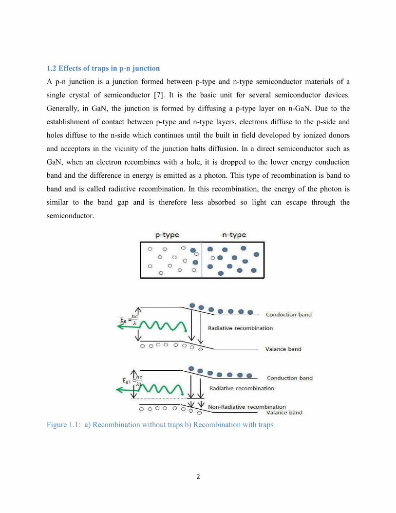
1.2 Effects of traps in p-n junction
A p-n junction is a junction formed between p-type and n-type semiconductor materials of a
single crystal of semiconductor [7]. It is the basic unit for several semiconductor devices.
Generally, in GaN, the junction is formed by diffusing a p-type layer on n-GaN. Due to the
establishment of contact between p-type and n-type layers, electrons diffuse to the p-side and
holes diffuse to the n-side which continues until the built in field developed by ionized donors
and acceptors in the vicinity of the junction halts diffusion. In a direct semiconductor such as
GaN, when an electron recombines with a hole, it is dropped to the lower energy conduction
band and the difference in energy is emitted as a photon. This type of recombination is band to
band and is called radiative recombination. In this recombination, the energy of the photon is
similar to the band gap and is therefore less absorbed so light can escape through the
semiconductor.
Figure 1.1: a) Recombination without traps b) Recombination with traps
Page 11
3
The wavelength of photon can be calculated by E = ���
E is the difference between valence and conduction band
h is planks constant; ℎ = 6.62606 10� � kg m2/s
λ is the wavelength of the emitted light
This is not the case when deep level defects are present in a semiconductor. These act like trap
centers at intermediate states in the band gap for electrons/holes. These traps prevent band to
band recombination of electrons with holes; rather recombination may take place at intermediate
levels with random wavelengths reducing intensity of light produced. This type of recombination
is called Shockley-Read-Hall recombination [48]. In this type of recombination, both radiative
and non-radiative recombination takes place. This does not occur in a perfectly pure
semiconductor. Intermediate recombination reduces the internal quantum efficiency of an LED.
The presence of deep level impurities is responsible for the current-voltage characteristic
collapse seen in III-nitride field effect transistors (FETs) [16-18].
1.3 Defect characterizing techniques
Many characterizing techniques for III-nitride semiconductors have been in use since researchers
found defects needing characterization. These techniques started in 1945 with the magnetic
resonance method called Electron Spin Resonance (ESR) [10]. ESR is used to find the
symmetry, nature and environment of paramagnetic defects. This method has been used for
several years to study defects in many semiconductors [11-14]. The sensitivity of ESR is on the
order of 1012 ions. Optically Detected Magnetic resonance (ODMR) is similar to ESR in
studying the nature and symmetry of traps except for the technique used. It is successfully used
in II-VI , III-V and amorphous Si [15]. Electrically detected magnetic resonance (EDMR)
observed spin dependent electrical properties of the semiconductor, which is mainly used for
GaN based devices. Later, positron annihilation spectroscopy is used to detect vacancy defects.
Thermalized positrons are trapped in vacant lattice sites, which reduce electron density and
increase lifetime. Detection of these quantities gives information like charge state, concentration
and defect atomic structure. This technique is especially used to detect vacancy defect states in
GaN epitaxial layers. In an effort to characterize different types of traps against a single variable,
find information about concentration, energy levels and capture rates of traps, distinguish
between majority and minority carrier traps and analyze both radiative and non-radiative centers,
a new technique Deep Level Transient Spectroscopy was developed by D.V. Lang [19]
Page 12
4
1.3.1 DLTS (Deep Level Transient Spectroscopy): DLTS investigates deep level traps in
semiconductor P-N junctions or Schottky barriers’ space charge region [20]. Capacitance
transients produced by pulsing the Schottky diode junction at different temperatures results in, a
spectrum being generated which exhibits a peak for each deep level. The height of the peak is
proportional to trap density, its sign allows one to distinguish between minority and majority
traps and the position of the peak leads to the determination of fundamental parameters
governing thermal emission, activation energy and cross section.
1.3.2 C-V (Capacitance – Voltage): “C-V measurements are well recognized for the valuable
information they yield about device and material characteristics” [6]. Capacitance measurement
with varying voltage across the p-n or the Schottky diode junction gives the C-V profile.
Semiconductor parameters like doping concentration, oxide charges and thickness, threshold
voltages and mobile ions can be determined by C-V measurements. Generally C-V is done on
Metal-Semiconductor junction, which creates a variable capacitance on applying voltage.
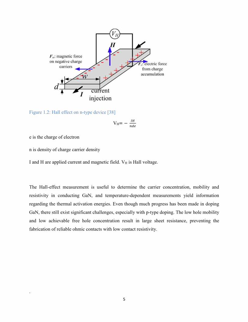
1.3.3 Hall Effect
Magnetic field exerts a transverse force on moving charges, or Lorentz force [39]. When a
current carrying material is placed in a magnetic field, the magnetic field exerts force on both
charges (semiconductor) in opposite directions. This accumulation of charges develops a voltage
difference across a conductive material called the Hall voltage and this effect is called the Hall
effect.
Page 13
5
Figure 1.2: Hall effect on n-type device [38]
VH= − �����
e is the charge of electron
n is density of charge carrier density
I and H are applied current and magnetic field. VH is Hall voltage.
The Hall-effect measurement is useful to determine the carrier concentration, mobility and
resistivity in conducting GaN, and temperature-dependent measurements yield information
regarding the thermal activation energies. Even though much progress has been made in doping
GaN, there still exist significant challenges, especially with p-type doping. The low hole mobility
and low achievable free hole concentration result in large sheet resistance, preventing the
fabrication of reliable ohmic contacts with low contact resistivity.
.
Page 14
6
Chapter 2: Literature Review
2.1 Overview: This chapter covers a brief history of Gallium nitride growth, defects, structure,
the study of traps and their formation.
The initial attempt to synthesize GaN was made by Juza and Hahn [43]. Later, Ammonia was
passed over hot gallium to synthesize the small needles of GaN. Using chemical vapor
deposition, Maruska and Titjen succeeded in growing GaN on sapphire substrates in 1969[2].
But there was not much technological advancement due to the p-type doping and poor
conductivity restrictions. It then became obvious that doping and defects would play a vital role
in the future development of GaN. The early unintentionally doped GaN was believed to be n-
type because of the nitrogen vacancies, which are reduced by the AlN buffer layer [23]. The
dislocation density for GaN ranges from 108 to 1012 cm-3[24]. The major defects in the GaN
epitaxial layer include stacking faults, small angle grain boundaries and nano pipes [25, 27].
Until the 1980s, the importance of carefully optimizing the geometry around defects and the
magnitudes of the relaxation energies were not fully realized [40].
The formation of defects depend on many factors, including growth conditions, level of doping,
type of impurities, substrate and buffer layer. The GaN grown by Metal-Organic Vapor Phase
Epitaxy (MOVPE) on the bulk platelets have a low density of defects [28] with proper cleaning
and growth conditions. The AlN/sapphire interface contains a high density of misfit dislocations,
which release almost all the misfit between their crystalline lattices at the growth temperature
[29]. The lateral overgrowth in III-nitrides is based on the difference in growth rates of GaN in
different crystallographic directions.
2.2 Gallium Nitride (GaN)
Gallium nitride is a III-V direct bandgap semiconductor. GaN generally exists in two different
crystal structures, as hexagonal Wurtzite and Cubic Zincblende. The former Wurtzite structure is
the stable one and the second Zincblende structure is a metastable one. Gallium nitride (GaN)
and its ternary and quaternary compounds are prime candidates for fabrication of visible,
ultraviolet high-power, high-performance optoelectronic and electronic devices. The physical
properties like wide energy band gap and good thermal stability of GaN make it an important
semiconductor material for high temperature and high power electronics. High thermal
Page 15
7
conductivity compared to silicon and GaAs, makes GaN a better material for heat dissipation in
devices.
Figure 2.1: Gallium nirtride Wurtzite crystal structure (Wikipedia [47])
Figure 2.2: Properties of GaN (Edgar 1994)
Page 16
8
Epitaxy or epitaxial growth is a technique in which a single crystal layer is grown on a substrate.
There are many ways to grow GaN. Metal organic Chemical Vapor deposition (MOCVD),
Molecular beam epitaxy (MBE) and Liquid Phase Epitaxy (LPE) are generally used. This DLTS
characterization is done on GaN grown by Korakakis’s group [56] using MOCVD.
2.3 Growth of GaN on MOCVD:
MOCVD is a fast and precise growth technique for many III-N materials. Metal organic
chemical vapor deposition (MOCVD) involves a dynamic flow in which gaseous reactants pass
over a heated substrate and react chemically to form a semiconductor layer. III-N materials were
grown using Trimethylgallium (TMGa), Trimethylaluminum (TMAl), Trimethylindium (TMIn),
Silane (SiH4) and Ammonia (NH3) as precursors. In (TF-MOCVD) technique, there are two gas
flows, main flow and sub flow [1]. The main flow carries reactant gases parallel to the substrate,
whereas sub flow gases are inactive and travel perpendicular to the substrate. This sub flow
gasses change the direction of the main flow, so that precursors come into contact with the
substrate.
Sapphire is used as a substrate with (0001) orientation. Trimethylgallium and Ammonia were
used as precursors. N2 and H2 gasses are used to carry metal organic precursors to the substrate,
which is heated to 1020°C in the stream of H2, and made to react on the surface to form films.
All this process requires a controlled vapor pressure and flow rate of reactants. Many concepts
have been developed to accomplish and optimize laminar flow of reactants.
The principal reaction to form GaN is
Ga (CH3)3(v) + NH3 GaN(s) + 3CH4 (v)
2.4 Traps
Traps are undesirable defects in the crystal lattice of semiconductor which have different energy
levels. Under a non-equilibrium state of a semiconductor, electron-hole pairs are generated.
After some time they return to equilibrium by electron-hole pair recombination. If the
recombination is between the electron in the conduction band and the hole in valence band then
it is called band to band recombination. If one of the carriers (electron or hole) is trapped
Page 17
9
between the bands and other carrier is free then this is called recombination on localized states.
This capture center of free carrier is called a trap.
Figure 2.3: Transitions in semiconductors a) band to band recombination b) recombination levels
c) trapping levels ( ASDN.NET eductional webportal[49])
LR1 , LR2 are local recombination levels.
Etn , Epn are trapping levels near conduction and valence band respectively.
Nt , Pt are concentrations of trapping levels near conduction and valence band respectively.
2.4.1Classification of defects
There are two types of traps, shallow traps and deep level traps. They are distinguished based on
the energy levels. Shallow traps exist in the band gap near the bottom of the conduction band or
near the top of the valence band. Generally for shallow traps, thermal ionization yields a free
carrier and an empty trap. Deep trap is defined by an energy level of trapped carriers whose
energy difference between it and the conduction band (for electrons) or valence band (for holes)
is much greater than the energy of thermal excitation of the solid at a given temperature.
Impurities, point defects, vacancies, interstitial defects, surface states and interface stresses can
act as trapping centers. Dislocation defects, which propagate from the substrate during epitaxy to
active region, cause a more rapid degradation of the device, which are not traps. The density of
Page 18
10
dislocations in active area can be reduced by small geometry and incorporation of the appropriate
buffer layer, which acts as dislocation filters [54].
All these defects which occur in GaN, can be characterized as follows [53]
a. Point defects, which are also called as zero dimensional defects associated with a single
atomic size.
b. Line defects, which are also called One-dimensional defects associated with a direction.
c. Planar defects, which are also called Two-dimensional defects associated with a plane or
area.
d. Volume defects, which are also called Three-dimensional defects associated with the
volume.
a. Point defects
There are three types of point defects, vacancies, interstitials and substitutional atom defects. If
an atom does not occupy a regular crystal site, but occupies a site between regular atoms, it is
called an interstitial impurity atom. When an impurity atom substitutes an atom of the host
crystal, it is a substitutional impurity. Substitutional impurity is introduced into the crystal either
by controlled doping or by contaminants. Oxygen and Carbon are generally the most common
contaminants that cause substitutional impurities. Point defects can be characterized as intrinsic
and extrinsic point defects. Intrinsic point defects occur due to vacancies, self- interstitial
impurities and antisites, as those impurities come from the crystal itself. Extrinsic point defects
involve foreign atoms, which occur due to substitutional impurities and interstitial impurities.
b. Line defects
Line defects occur due to the dislocations of atoms. Dislocations occur due to misalignment of
atoms or presence of vacancies along a dislocation line in the solid. Dislocations create elastic
deformations of the lattice at large distances that cause lattice distortion centered around a line.
There are three types of dislocations namely Edge dislocation, Screw dislocation and Mixed
dislocation which is both edge and screw dislocations.
c. Planar defects
Planar defects are related to Stacking faults, Stacking mismatch boundaries, Grain boundaries
and Twins. Stacking faults are partial displacements, which upset the regular sequence of lattice
planes stacking. Stacking mismatch boundaries originate at the substrate or film interface.
Page 19
11
Surface steps on a substrate that cause nucleation and growth of separate III-nitrides at different
levels create them. Grains of single crystals are present in Polycrystalline materials with different
crystallographic orientation. A layer of interconnecting boundary atoms surrounds each grain and
it is called a grain boundary. A twin is a defect area, in which a mirror image of the regular
lattice is formed. The twin boundary is the mirror plane of the twin formation. The atomic
displacements during the twinning increase with the distance from the boundary.
d. Volume defects
The volume defects are related to Inversion domains and Nano pipes. This defect originates from
the nucleation layer and has a filamentary nature. Defects due to nanopipes are tunnel like
defects that are always aligned along the growth direction of the crystal. The majority of defects
are generated at the interfaces with the substrate and the buffer layer. Lattice matching in
epitaxial growth is essential between epitaxial layers and the substrate/material on which
material is growing. It can be done by choosing substrate/material with a same lattice constant.
This can also be done by growing a buffer layer in between material and substrate/material. Here
through MOCVD grown GaN, AlN is used as a buffer layer to match the lattice. The structural
quality of the GaN layer can be controlled by the growth conditions, especially during the first
growth stages.
2.5 Charging and Discharging of Traps in space charge region
Traps charge and discharge with bias. When the bias V0 is applied to Schottky diode for time tp
the traps fill exponentially with electrons. Traps spill out electrons exponentially under lower
bias Vb, which is also referred to as the electron emission from traps. The exponential decay
depends on the concentration of filling traps (�� ,t=0) and the emission rate (en). [51]
����� = ���� = 0� �����
The time constant τ of the thermal emission is governed by the thermal emission rate en, which
depends on the trap energy Et and on the temperature T
Page 20
12
Figure 2.4: Filling and emptying of deep level traps with different bias a)higher bias V0 b)lower
bias Vb ( [50])
The emission probability per second en is given by
en = � =
!"#$% �&'()*+*
Where σ is the trap’s capture cross section, v is the average thermal velocity of electrons, Nc is
the effective density of states in the conduction band, and ET
is the energy difference between the
trap level and the conduction band [52].
Figure 2.5: Band diagram of n-type GaN with trap levels
Page 21
13
Table 2.1: Typical Trap properties of MOCVD grown GaN(Hadis Markoc[55])
Trap
number
Trap peak temp (T) in
°K
Concentration(cm-3)
Energy(eV)
Capture cross section(cm2)
1.
150
2.4*1013
0.246
2.4*10-13
2.
325
6.6*1015
0.536
5*10-16
3.
520
9.6*1013
0.92
1*10-15
The two traps shown in Figure 2.5 are commonly observed in n- GaN. Trap E1 concentrations
are lower in n-GaN grown on an n+ GaN substrate, suggesting its correlation with dislocations
[56]. The DLTS peak amplitude of trap E1 varies with filling pulse time tp. This is due to the line
defect formed by dislocations. On the other hand, E2 is a dominant peak and the peak increases
with increase in Si doping concentration, which induces point defects. This peak can be reduced
by doping with In which reduce point defects including native defects.
Page 22
14
Chapter 3: DEEP LEVEL TRANSIENT SPECTROSCOPY OF GaN
3.1 Overview
This chapter explains Capacitance-Voltage and Deep Level Transient Spectroscopy techniques.
Each technique explanation covers the physics involved and the experimental procedures for
acquisition. DLTS measurements are taken after determination of the doping concentration of the
semiconductor by C-V measurements.
3.2 Capacitance – Voltage (CV) measurements
C-V is one of the electrical characterizing techniques for semiconductors. It requires either a
Schottky diode or p-n junction which forms a space charge region. For this study, p-GaN and n-
GaN Schottky diodes are used.
A Schottky diode is a metal semiconductor junction. Before understanding the concept in a metal
semiconductor junction let’s examine a p-n junction.
Figure 3-1: p-n junction depletion layer with Nd > Na (Ben G.streetman [36])
Page 23
15
Figure 3-2: charge density with in depletion region neglecting free carriers (Ben
G.Streetman [36])
When a junction is formed, free carriers diffuse and recombine across the junction to form a
depletion layer which is void of free carriers. This region is also called a space charge region.
Considering no free carriers in the space charge region, the charge density in the n-type volume
within the space charge region is given by q multiplied by the donor concentration Nd and
similarly the charge on p side is –q multiplied by the acceptor concentration Na. Depending on
the concentration, the depletion region may vary its distance into p or n type. In the above p-n
junction, doping on the n-side is more than the p-side i.e. Na < Nd so depletion layer extends
more into p-side. Generalizing charge density for a junction with a cross sectional area A, charge
on either side of the dipole is equal and can be written as
q A xno Nd = q A xpo Na 3.1
xno is distance encroachment by depletion layer into n-side.
xpo is distance encroachment by depletion layer into P-side.
A potential difference develops over the space charge region from n-side to p-side due to the
barrier caused by no charge carriers in this region. Using Poisson’s equation (∇. E = ./0 ) the
gradient of the electric field is define as
�1�2 = 3
ε Nd , 0 < x < xno
�1�2 = 3
ε Na, – xpo < x < 0
Where, 45 is free charge density.
Page 24
16
Considering E is zero at the edges of depletion layer, and maximum at center since all electric
lines passes thorough x=0 plane. Let E0 be the maximum electric field.
6 789:; = 3
ε Nd 6 7&>?;9 , 0 < x < xno
6 781@9 = – 3
ε Nd 6 7&9�BC@ , – xpo < x < 0
The maximum value of electric field is E0 = − 3ε Nd xno = − 3
ε Na xpo
By using the relation between voltage and electric field, V0 = − 6 8�&�B�@�BC@ 7&
V0 = − �D 8E F = �
D3ε xno Nd W = − �
D3ε xp0 Na
We know W = xpo + xno and solving for W using 3-1
V0 = �D
3ε #G#�
#GH#� FD
W = IDεJ KE L �
#G + �#�NO
�/D 3.2
This shows that the depletion width of a p-n junction is dependent on the contact potential and
doping concentrations. Since we are taking C-V measurements on a Schottky diode, the above
equation 3.2 is transformed such that it satisfies Schottky diode properties. The major differences
between a Schottky barrier and a p-n junction are its typically lower junction voltage, and
decreased (almost nonexistent) depletion width in the metal [32]. Since the depletion layer in the
metal is so small it can be neglected, and therefore all the depletion and potential difference
occur in the semiconductor.
Page 25
17
3.2.1 Schottky diodes in n-type GaN
Ni/Au unannealed and Ti/Al/Ti/Au annealed metal contacts are deposited on n-type GaN for
Schottky contact and ohmic contact respectively, which forms a Schottky diode. Formation of a
Schottky diode on N-type GaN is clearly explained in chapters 4 & 5.
Figure 3-3: a) Metal semiconductor before contact b) Metal semiconductor after contact
(Gísli Jóhann Grétarsson[31])
Figure 3-4: Junction formation in metal and n type semiconductor (Ben G.streetman [36])
The electric field and bending of bands within a depletion layer are similar to p-n junction. Here
a depletion layer only formed in the semiconductor. Negative charge on the metal is formed
because of the positive charge of uncompensated donor ions near the junction. So, W can be
calculated by p+- n approximation using 3.2. In a p+- n junction, neglecting the thin sheet of the
Page 26
18
positive layer (xp0 = 0) and QR ≫ Q7. This implies �
#G << �#� and W = xno , replacing these
quantities in 3.2.
Now, xno = IDεJ KE L �
#�NO�/D
3.3
3.2.2 Schottky diodes in p-type GaN
Ni/Au annealed and Ti/Al/Ti/Au metal contacts are deposited on P-type GaN for ohmic contact
and Schottky contact respectively, which forms a Schottky diode. Formation of a Schottky diode
on N-type GaN is clearly explained in chapters 4 & 5.
Figure 3-5:Junction formation in metal and p type semiconductor (Ben G.streetman [36])
When the junction is formed, positive charge is induced on metal due to the negative
uncompensated acceptors. Using 3.2,
Xpo = IDεJ KE L �
#GNO�/D
3.4
3.3 C-V Analysis
A Schottky diode is fabricated on a GaN substrate. In a Schottky diode, metal and semiconductor
acts as plates of a capacitor and the depletion region acts as an insulator. This formation gives the
capacitance effect which is used to characterize semiconductors by C-V measurements.
Capacitance in the parallel plate capacitor is given by
C = ε ; ε U V
W 3.5
d is the depletion layer width (in case of Schottky diode)
Page 27
19
εr is relative permittivity
ε0 is the permittivity of free space
Let’s consider n-type first, When a reverse bias voltage Vr is applied to a Schottky diode the built
in voltage increases which is equal to V0 + Vr and here d = xno . From 3.3 and 3.5, and
substituting these quantities we get
Nd = −2 XYZ3[U [9\Y = −2 X]
3[U [9\Y L �X�Z^N��
3.6
Similarly for p-type
Na = −2 XYZ3[U [9\Y = −2 X]
3[U [9\Y L �X�Z^N��
3.7
This is the most useful form, deduced by Hilibrand and Gold. This is used to calculate bulk
doping concentration of a semiconductor. By calculating the slope of the graph � �XY� versus V,
the doping concentration of the semiconductor is known. V0 , built in voltage can also be
calculated by finding the x-intercept of the graph. [33]
Figure 3-6: C-V measurement graph ( Miron J. Cristea[33])
Page 28
20
3.4 Deep Level Transient Spectroscopy (DLTS)
DLTS is based on the fact that the capacitance of the space charge region in time depends on the
charge state of deep level traps in that region [34]. From 3.6 we can write the capacitance of the
junction is
_E = ` a[[;J�bW�DZ 3.8
V= Vo + Vr
Where Vo is the built in voltage and Vr is the reverse bias voltage.
Nd is ionized donor in the space charge region.
Including concentration of traps in the math, let Nt is the trap concentration present in n-sample.
Capacitance of the junction now changes due to the extra traps in the depletion region.
Ct = ` a[[;J�bWHbc�D�d; H dU� 3.9
Thus the change in capacitance due to recharging these levels is given by
ΔC = ` a [[;J�bW�D�d; H dU� − ` a[[;J�bWHbc�
D�d; H dU�
≡ C0 #�
D�#�� when Nt << Nd 3.10
From 3.10 traps concentration can be calculated
Nt = DefX@ Q7 3.11
Page 29
21
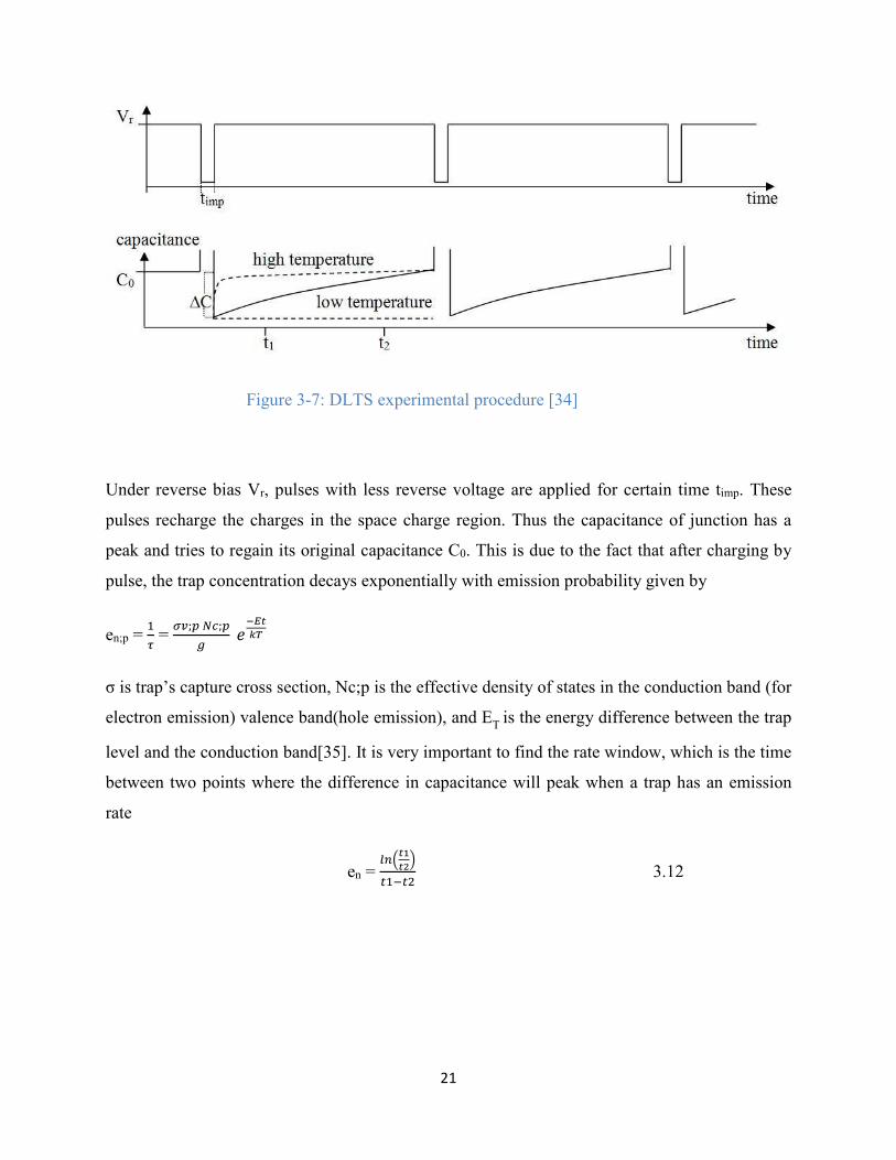
Figure 3-7: DLTS experimental procedure [34]
Under reverse bias Vr, pulses with less reverse voltage are applied for certain time timp. These
pulses recharge the charges in the space charge region. Thus the capacitance of junction has a
peak and tries to regain its original capacitance C0. This is due to the fact that after charging by
pulse, the trap concentration decays exponentially with emission probability given by
en;p = �g =
h";C #�;C% �()j
+*
σ is trap’s capture cross section, Nc;p is the effective density of states in the conduction band (for
electron emission) valence band(hole emission), and ET
is the energy difference between the trap
level and the conduction band[35]. It is very important to find the rate window, which is the time
between two points where the difference in capacitance will peak when a trap has an emission
rate
en = k�Ljl
jYN����D 3.12
Page 30
22
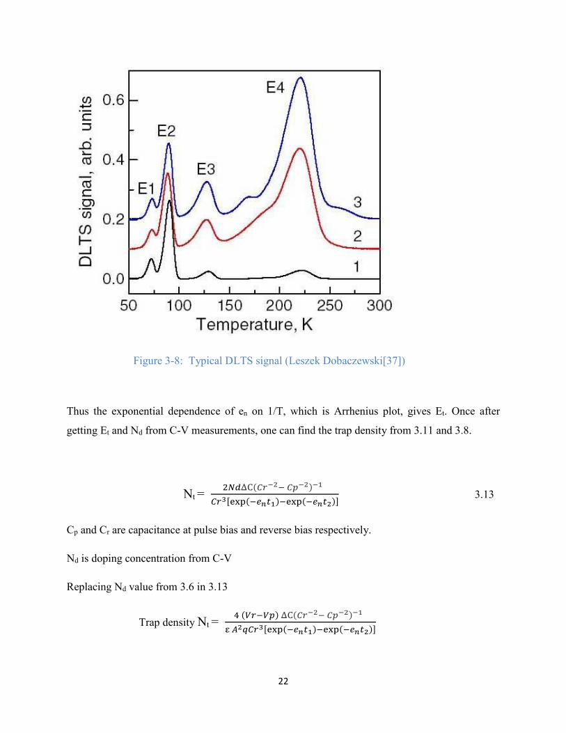
Figure 3-8: Typical DLTS signal (Leszek Dobaczewski[37])
Thus the exponential dependence of en on 1/T, which is Arrhenius plot, gives Et. Once after
getting Et and Nd from C-V measurements, one can find the trap density from 3.11 and 3.8.
Nt = D#�ef�X^(Y� XC(Y�(l
X^]mnop�����l��nop�����Y�q 3.13
Cp and Cr are capacitance at pulse bias and reverse bias respectively.
Nd is doping concentration from C-V
Replacing Nd value from 3.6 in 3.13
Trap density Nt = � �Z^�ZC� ef�X^(Y� XC(Y�(l
[ \Y3X^]mnop�����l��nop�����Y�q
Page 31
23
Chapter 4: Metal Contacts on GaN
Metal contacts are essential to form a space charge region for defect characterization using
DLTS. p-n junction properties can be achieved by simple metal semiconductor contact.
Moreover they are useful when high speed rectification is needed and sometimes metal
semiconductor junctions are unavoidable in semiconductors. This chapter deals with Schottky
and Ohmic contacts on both n-GaN and p-GaN.
4.1 Schottky Contact
The Schottky barrier is the rectifying barrier for electrical conduction across heterojunction
[64]. Schottky contacts are formed between metal and semiconductor materials if there is a large
barrier height and also very low doping concentration in the semiconductor material that is less
than the density of states in the conduction band or the valence band [58]. The current-voltage
characteristics of rectifying metal semiconductor junctions are similar to p-n junction. They
differ in current flow and carrier participation. A p-n junction is a bipolar device, whereas
Schottky diodes are unipolar devices [62]. The current in Schottky diode is mainly due to the
thermionic emission [65], which will be discussed later in this chapter, of carriers over the
potential barrier at metal-semiconductor junction [63].
4.1.1 Schottky contact on n-type
When a metal with work function qØm is brought in contact with semiconductor having work
function qØs, the semiconductor Fermi level is higher than metal Øm > Øs so few electrons move
from semiconductor to lower energy states in the metal until Fermi levels align at equilibrium.
As a result band bending occurs. Then there exists a potential barrier (qØi) which prevents
electrons and holes from passing one side to another, which is the difference in work function
potentials q(Øm – Øs). Similarly barrier height Øb prevents electron injection from the metal into
a semiconductor conduction band which is q(Øm – χ )
Due to charge neutrality, positively ionized donors in the depletion region of semiconductor are
balanced by a sheet of electrons in the metal at the junction. The potential barrier is increased or
decreased by applying bias voltage. Schottky contacts, conduct for one bias polarity so they are
also called rectifying contacts. The reduction of work function due to the induced positive charge
Page 32
24
in metals by negative charges in the semiconductor causes barrier lowering which is referred to
as the Schottky effect.
The Energy band diagrams below clearly show the contact characteristics.
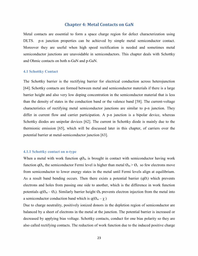
Figure 4-1: Energy band diagram of metal and n-type semiconductor (Øm > Øs ) a) before
contact b) just in contact c) thermal equilibrium (B. Van Zeghbroeck, 2011) [59]
Øb is the barrier height, which is the potential difference between the Fermi energy of the metal
and the majority carrier band edge.
Øm is the work function of metal.
Øi is the built in potential which is the difference between the Fermi energy of metal and that of
semiconductors.
For an n-type semiconductor the barrier height is given by Øb = Øm – χ.
Built in potential Vb is the difference between the Fermi energy of the metal and the
semiconductor.
Vb = ØM – χ – �1r�1s,��
3 , n-type
Where ‘χ ‘ is electron affinity of semiconductor. Therefore a metal-semiconductor junction forms
a barrier when the Fermi energy of metal is somewhere between the conduction and valence
band edge. [59]
a) b)
c)
Page 33
25
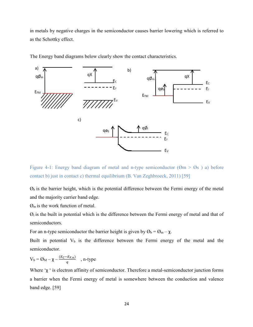
Figure 4-2: Current Voltage characteristics of Schottky contact on n-type GaN
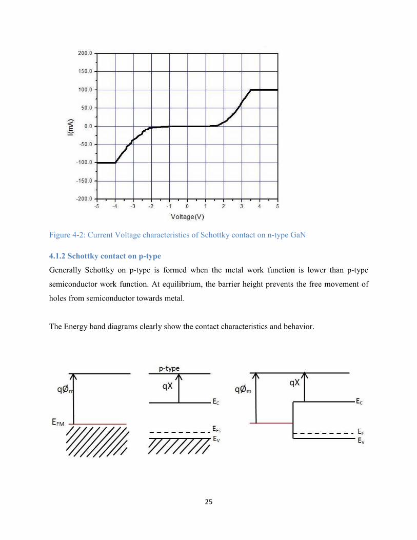
4.1.2 Schottky contact on p-type
Generally Schottky on p-type is formed when the metal work function is lower than p-type
semiconductor work function. At equilibrium, the barrier height prevents the free movement of
holes from semiconductor towards metal.
The Energy band diagrams clearly show the contact characteristics and behavior.
Page 34
26
Figure 4-3:Energy band diagram of metal and p-type semiconductor a) before b) just in contact
c) thermal equilibrium (B. Van Zeghbroeck, 2011)[59]
For p-type material, the barrier height is the difference between the valence band edge, and the
Fermi energy in the metal is given by Øb = Eg/2 + χ – Øm, where ‘χ ‘ is electron affinity of
semiconductor.
Vb = χ + �1r�1s,��
3 – ØM , p-type
Figure 4-4: Current Voltage characteristics of Schottky contact on p-type GaN
Page 35
27
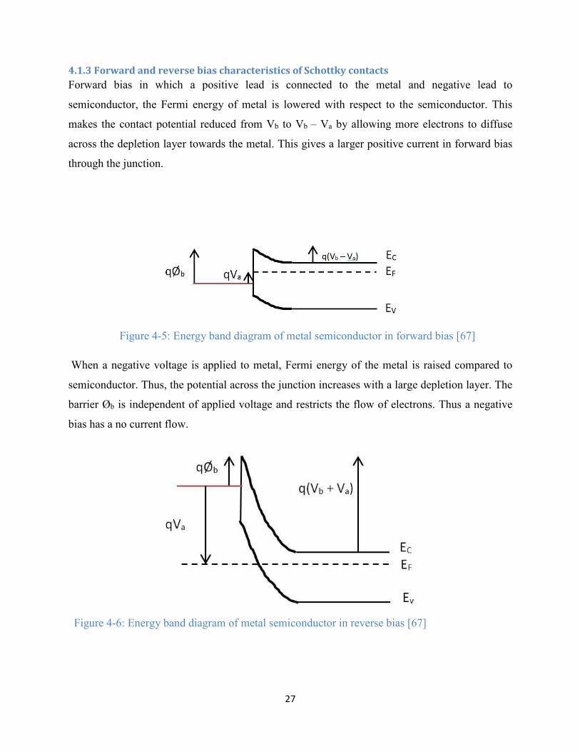
4.1.3 Forward and reverse bias characteristics of Schottky contacts
Forward bias in which a positive lead is connected to the metal and negative lead to
semiconductor, the Fermi energy of metal is lowered with respect to the semiconductor. This
makes the contact potential reduced from Vb to Vb – Va by allowing more electrons to diffuse
across the depletion layer towards the metal. This gives a larger positive current in forward bias
through the junction.
Figure 4-5: Energy band diagram of metal semiconductor in forward bias [67]
When a negative voltage is applied to metal, Fermi energy of the metal is raised compared to
semiconductor. Thus, the potential across the junction increases with a large depletion layer. The
barrier Øb is independent of applied voltage and restricts the flow of electrons. Thus a negative
bias has a no current flow.
Figure 4-6: Energy band diagram of metal semiconductor in reverse bias [67]
Page 36
28
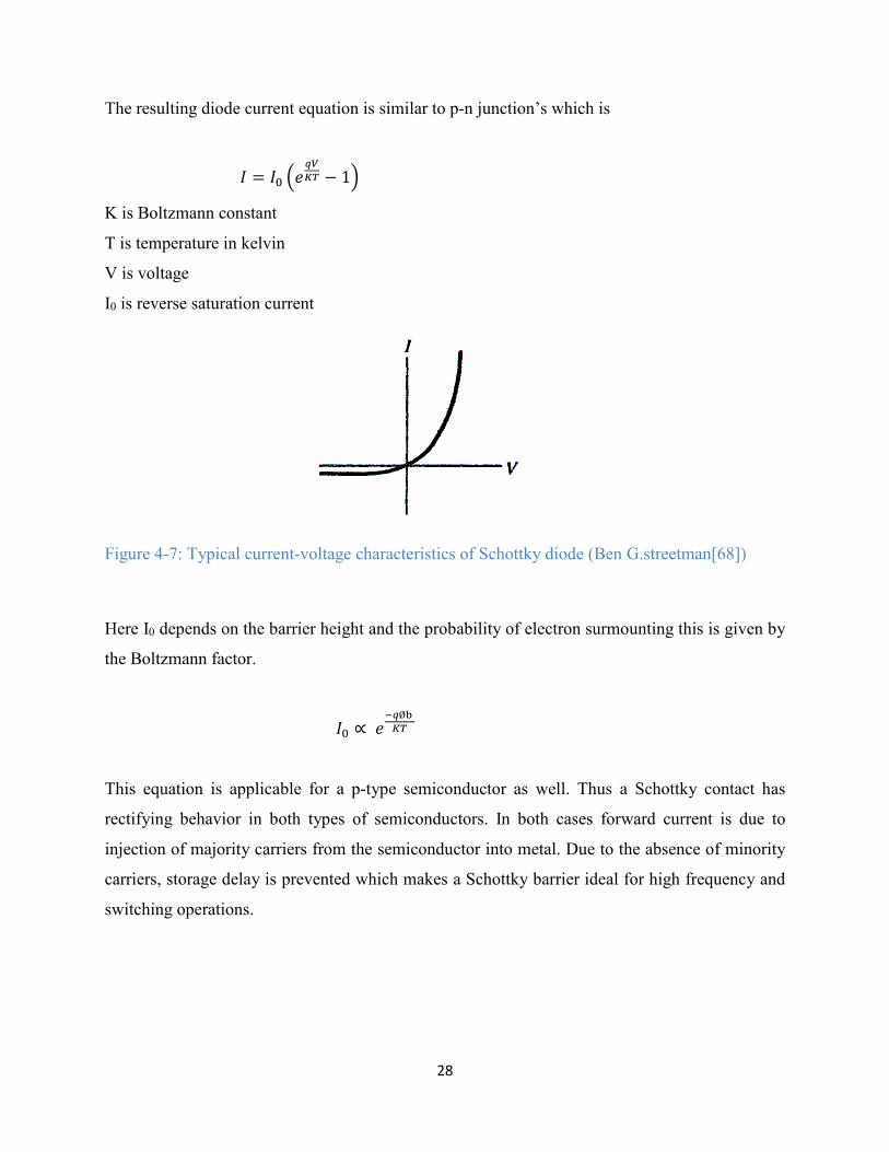
The resulting diode current equation is similar to p-n junction’s which is
t = t9 L�uvw* − 1N
K is Boltzmann constant
T is temperature in kelvin
V is voltage
I0 is reverse saturation current
Figure 4-7: Typical current-voltage characteristics of Schottky diode (Ben G.streetman[68])
Here I0 depends on the barrier height and the probability of electron surmounting this is given by
the Boltzmann factor.
t9 ∝ �(uØz w*
This equation is applicable for a p-type semiconductor as well. Thus a Schottky contact has
rectifying behavior in both types of semiconductors. In both cases forward current is due to
injection of majority carriers from the semiconductor into metal. Due to the absence of minority
carriers, storage delay is prevented which makes a Schottky barrier ideal for high frequency and
switching operations.
Page 37
29
4.2 Ohmic Contacts
Regardless of the application, voltage and current signals must be brought into, and taken out of
the semiconductors through electrical contacts, which must play a critical role of exhibiting a
linear relation with respect to applied voltage. These contacts are Ohmic contacts with low
contact resistance which does not hinder performance, especially at high frequency and high
power where parasitic contact resistance will limit both frequency and power handling [60,61].
There are many requirements in which I-V characteristics should be linear in both biasing
conditions and this can be achieved with ohmic contacts. Ohmic contacts are formed when the
work function of metal Øm is close to the semiconductors Fermi level Øs.
4.2.1 Ohmic contacts on n-type GaN
The energy band diagram below clearly shows the contact characteristics.
Figure 4-8: Ohmic metal n-type semiconductor contact band diagram a) Before contact b) At
equilibrium (Streetman [68])
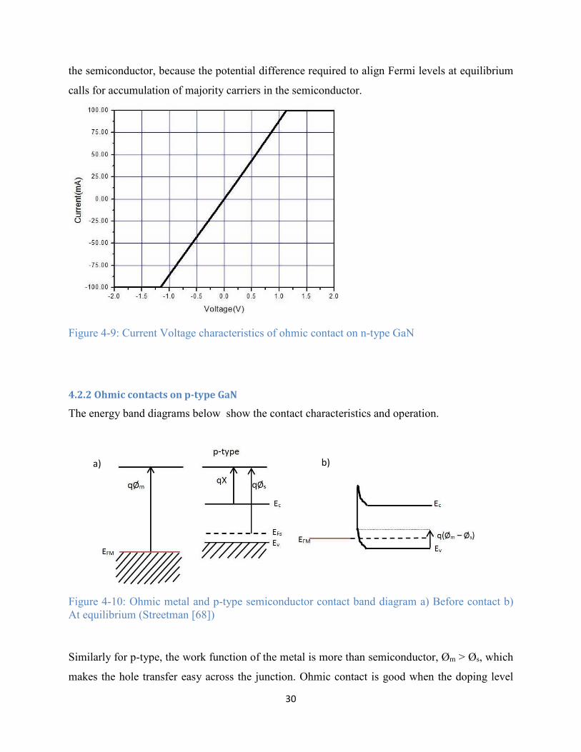
For n-type material when the work function of the metal is less than the work function of the
semiconductor i.e. Øm < Øs, at equilibrium, electrons transfer from metal to semiconductor. This
makes the metal Fermi level move downward. Here the barrier to electron flow from metal to
semiconductor is small and can be overcome by a small voltage. There is no depletion region in
a) b)
Page 38
30
the semiconductor, because the potential difference required to align Fermi levels at equilibrium
calls for accumulation of majority carriers in the semiconductor.
Figure 4-9: Current Voltage characteristics of ohmic contact on n-type GaN
4.2.2 Ohmic contacts on p-type GaN
The energy band diagrams below show the contact characteristics and operation.
Figure 4-10: Ohmic metal and p-type semiconductor contact band diagram a) Before contact b)
At equilibrium (Streetman [68])
Similarly for p-type, the work function of the metal is more than semiconductor, Øm > Øs, which
makes the hole transfer easy across the junction. Ohmic contact is good when the doping level
a) b)
Page 39
31
near the semiconductor surface is as high as possible. This causes the tunneling with low contact
resistance. For p-type, it is difficult to find metals with large enough work function (most metals
have less than 5V) to form a good ohmic contact.
Figure 4-8: Current Voltage characteristics of ohmic contact on p-type GaN
Table 4-1: Ohmic metal contact parameters of on GaN.
metallizatio
n scheme
Layer thickness Condition
to form
Ohmic
contact
Work
function(eV)
Specific
contact
resistivity
Ohm.cm2
Annealed
contacts
n-GaN Ti/Al/Ti/Au 30nm(Ni),
200nm(Au)
Øm close
to Øs
Øm= 4.33
Øs = 4.2-4.3
5.43E-5 Yes
p-GaN Ni/Au 2nm(Ti),100nm(Al),
30nm(Ti),200nm(Au)
Øm close
to Øs
Øm= 5.35
Øs = 7.3
1.34E-2 Yes
Table 4-2: Schottky metal contact parameters on GaN.
metallizatio
n scheme
Layer thickness Condition to
form Schottky
contact
Work
function(eV)
Built in
potential(eV)
Annealed
contacts
n-GaN Ni/Au 30nm(Ni),
200nm(Au)
Øm > Øs Øm= 5.35
Øs = 4.2-4.3
V0 = 1.1 No
p-GaN Ti/Al/Ti/Au 2nm(Ti),100nm(Al),
30nm(Ti),200nm(Au)
Øm < Øs Øm= 4.33
Øs = 7.3
V0 = 3 No
4.3 Conduction mechanisms in metal-semiconductor contacts
There are different ways in which conduction takes place in a Schottky contact.
Page 40
32
1. Thermionic emission: Thermionic emission is one in which electrons emit over the
barrier. It assumes the electron has greater energy than the barrier to overcome it. This
happens when the doping level is low, on the order Nd < 1017 cm-3. Due to low doping
the chance of tunneling is very much less. [66]
Figure 4-9: Thermionic emission band diagram and I-V curve[66]
2. Thermionic field emission: Thermionic field emission is another type of conduction, in
which electrons use thermal energy to tunnel through the thin barrier of upper end of the
conduction band. This is more likely when doping level is intermediate 1017 cm-3 < Nd <
1018 cm-3.
Figure 4-10: Thermionic-field emission [66]
3. Field emission: Field emission exists when the doping is very high. Here the conduction
is almost ohmic-like due to the direct tunneling, which is caused by a narrow depletion
layer. The doping concentration is Nd > 1018 cm-3
Page 41
33
Figure 4-11: Field emission [66]
From simulation results, Fig.4-15 shows that with increase in the doping concentration, the
depletion width of the junction decreases. For Nd > 1018, the depletion width is on the order of
few hundreds of nm. Here tunneling is easy and the conduction mechanism is field emission.
Figure 4-15: Plot of Depletion width against bias voltage for different doping concentrations.
Page 42
34
Chapter 5: Schottky Diode fabrication
Deep Level Transient Spectroscopy (DLTS) measurements require both Ohmic and Schottky
contacts. A Schottky diode for DLTS characterization is designed using the Circular
Transmission Line Method (CTLM) and fabricated. All the steps, materials and equipment used
for this fabrication are explained in this chapter.
5.1 Sample Annealing
Rapid Thermal Annealing (RTA) is a semiconductor process step used for activation of dopants
and interfacial reaction of metal contacts. The thermal treatment reduces resistivity by up to six
orders of magnitude, thus increasing conductivity [76]. The resistivity of the p-GaN was lowest
when O2 was intentionally introduced during activation [77].
For activation of Mg dopants, p-GaN is annealed at 800°C in N2 ambient for 5minutes. During
annealing there may be chances of forming a thin oxide layer over the substrate.
Figure 5-12: Side and top view of p-GaN substrate
Figure 5-13: Side and Top view of p-GaN with oxide layer after annealing
RTA is used only for p-GaN processing due to its characteristic high resistivity. At room
temperature, all dopants in n-type GaN are activated so no RTA is required for n-type GaN.
Page 43
35
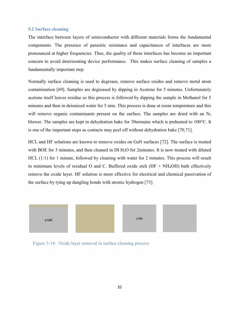
5.2 Surface cleaning
The interface between layers of semiconductor with different materials forms the fundamental
components. The presence of parasitic resistance and capacitances of interfaces are more
pronounced at higher frequencies. Thus, the quality of these interfaces has become an important
concern to avoid deteriorating device performance. This makes surface cleaning of samples a
fundamentally important step.
Normally surface cleaning is used to degrease, remove surface oxides and remove metal atom
contamination [69]. Samples are degreased by dipping in Acetone for 5 minutes. Unfortunately
acetone itself leaves residue so this process is followed by dipping the sample in Methanol for 5
minutes and then in deionized water for 5 min. This process is done at room temperature and this
will remove organic contaminants present on the surface. The samples are dried with an N2
blower. The samples are kept in dehydration bake for 30minutes which is preheated to 100°C. It
is one of the important steps as contacts may peel off without dehydration bake [70,71].
HCL and HF solutions are known to remove oxides on GaN surfaces [72]. The surface is treated
with BOE for 3 minutes, and then cleaned in DI H2O for 2minutes. It is now treated with diluted
HCL (1:1) for 1 minute, followed by cleaning with water for 2 minutes. This process will result
in minimum levels of residual O and C. Buffered oxide etch (HF + NH4OH) bath effectively
remove the oxide layer. HF solution is more effective for electrical and chemical passivation of
the surface by tying up dangling bonds with atomic hydrogen [73].
Figure 5-14: Oxide layer removal in surface cleaning process
Page 44
36
Figure 5-15: Flow chart of Schottky diode fabrication.
Layer1
5.3 Photolithography
Photolithography is the micro fabrication process of transferring geometric shapes on a mask to
the surface of semiconductor wafer [74]. The process uses light to transfer patterns from mask to
light-sensitive chemical called photoresist followed by a series of chemical treatments, to
develop the photoresist pattern exposed to light [75] which finally forms patterns on
semiconductor.
Page 45
37
There are many steps involved depending on the type of photo resist used: Photoresist
application or spinning, soft baking, mask alignment, hard baking, exposure and development.
5.3.1 Spinning: It is a process in which photoresist is uniformly deposited to a specified
thickness on surface of substrate. A small quantity of photoresist is usually applied on the center
of the wafer and the spun on a spinner which makes the photoresist spread uniformly. The
thickness depends on the viscosity of photoresist, spinning speed and time. There are two types
of photo resists - positive and negative. For positive resists, the resist is exposed to UV light
wherever the underlying material is to be removed. In these resists, exposure to the UV light
changes the chemical structure of the resist so that it becomes more soluble in the developer [78].
Negative resists behave just in the opposite manner. There are special photoresists which are
used in “lift off” techniques which call for a negative wall profile. Even though they are positive
resists they are capable of image reversal (IR) resulting in negative patterns on the mask. In this
work, a Laurel Technologies 400 spinner is used for spinning image reversal photoresist AZ
5214 for 30 seconds with speed 4000RPM. The thickness obtained for photoresist applied in
those conditions is 1.4μm.
Figure 5-16: AZ 5214 photoresist coating on GaN substrate
5.3.2 Soft bake: The photo resist coated wafer is prebaked to drive off the excess photoresist
solvent on a hot plate at 95°C for 1 minute. This is a critical step as excessive baking destroys
photoactive compound and reduces sensitivity. [79]
5.3.3 Mask Alignment and Exposure: It is the next step after soft bake, in which UV light is
exposed through a mask on the resist to change the solubility properties. The mask is a square
plate with a patterned emulsion of metal film on one side. There are three primary exposure
methods - contact, proximity and projection depending on the alignment gap between wafer and
mask.
Page 46
38
Figure 5-17: Contact, proximity and projection exposure methods (ece,gatech) [74]
For the process used here, the soft baked substrate is placed in proximity exposure in a
Suss MA6 Mask Microtech Aligner and UV light (i-line) of intensity 50mJ/cm2 is illuminated for
the time given by
� = {9|��|}�}"}�~ s
Figure 5-18: a) mask with ring pattern b) side view and top view of GaN during exposure in
mask aligner
Page 47
39
5.3.4 Hard bake or post exposure bake: In a hard bake, the substrate is baked on a hotplate for
1minute at 120°C-130°C. Image reversal capability to resist is obtained by a crosslinking agent
in the resist which becomes active at temperatures above 110°C for areas which are exposed in
mask aligner. After hard bake the exposed areas become insoluble and no longer light sensitive
while the unexposed areas still behave like normal photoresist.
Figure 5-19: side and top view of GaN after hard bake
5.3.5 Flood Exposure: A flood exposure of UV light in which no mask is used with intensity
2000 mJ/cm2 will now cause all previously unexposed areas of the resist to undergo chemical
reaction to make them soluble in developer. OAI UV flood exposure is used to illuminate 365nm
UV light. The exposure time is approximately
� = D999|��|}�}"}�~s.
Figure 5-20: side and top view of GaN in flood exposure
Page 48
40
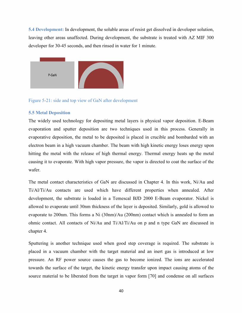
5.4 Development: In development, the soluble areas of resist get dissolved in developer solution,
leaving other areas unaffected. During development, the substrate is treated with AZ MIF 300
developer for 30-45 seconds, and then rinsed in water for 1 minute.
Figure 5-21: side and top view of GaN after development
5.5 Metal Deposition
The widely used technology for depositing metal layers is physical vapor deposition. E-Beam
evaporation and sputter deposition are two techniques used in this process. Generally in
evaporative deposition, the metal to be deposited is placed in crucible and bombarded with an
electron beam in a high vacuum chamber. The beam with high kinetic energy loses energy upon
hitting the metal with the release of high thermal energy. Thermal energy heats up the metal
causing it to evaporate. With high vapor pressure, the vapor is directed to coat the surface of the
wafer.
The metal contact characteristics of GaN are discussed in Chapter 4. In this work, Ni/Au and
Ti/Al/Ti/Au contacts are used which have different properties when annealed. After
development, the substrate is loaded in a Temescal BJD 2000 E-Beam evaporator. Nickel is
allowed to evaporate until 30nm thickness of the layer is deposited. Similarly, gold is allowed to
evaporate to 200nm. This forms a Ni (30nm)/Au (200nm) contact which is annealed to form an
ohmic contact. All contacts of Ni/Au and Ti/Al/Ti/Au on p and n type GaN are discussed in
chapter 4.
Sputtering is another technique used when good step coverage is required. The substrate is
placed in a vacuum chamber with the target material and an inert gas is introduced at low
pressure. An RF power source causes the gas to become ionized. The ions are accelerated
towards the surface of the target, the kinetic energy transfer upon impact causing atoms of the
source material to be liberated from the target in vapor form [70] and condense on all surfaces
Page 49
41
including the substrate. In this the material is released from the source at a much lower
temperature than evaporation.
A Magnetic field can be used to confine electrons near the target surface to greatly increase the
possibility of ionizing collisions with the argon gas molecules.
Figure 5-22: side and top view of GaN after metal deposition
5.6 Lift Off
Lift off is an additive technique with photoresist as a sacrificial material. Metal is applied over
the patterned photoresist. During this process, the substrate is dipped in acetone for 15 minutes.
Photoresist and the metal deposited above it will be removed completely, leaving the metal in a
mask pattern shape on the underlying substrate.
Figure 5-23: Side and top view of GaN after lift off
Page 50
42
5.7 Contacts Annealing
Rapid thermal annealing is also used for contact annealing to modify its structural properties.
AnnealSys AS-Micro Rapid Thermal Annealer has a process chamber made of a quartz tube with
water cooled stainless steel flanges. An infrared halogen lamp is used as a heating source [data
sheet]. The chamber is coated with reflective coatings to reduce thermal loss and improve
uniformity [81]. For contacts annealing the recipe used is 600°C in O2 ambient for 3 minutes.
Second layer: For the second layer Schottky dot fabrication, all steps are similar to the first layer
starting from spinning to lift. For the Schottky dot a new mask shown in fig. 5-13 and
Ti/Al/Ti/Au metal composition are used.
Figure 5-24: Mask with dot pattern
Page 51
43
Figure 5-25: Schottky contact fabrication process
Page 52
44
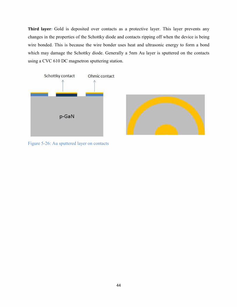
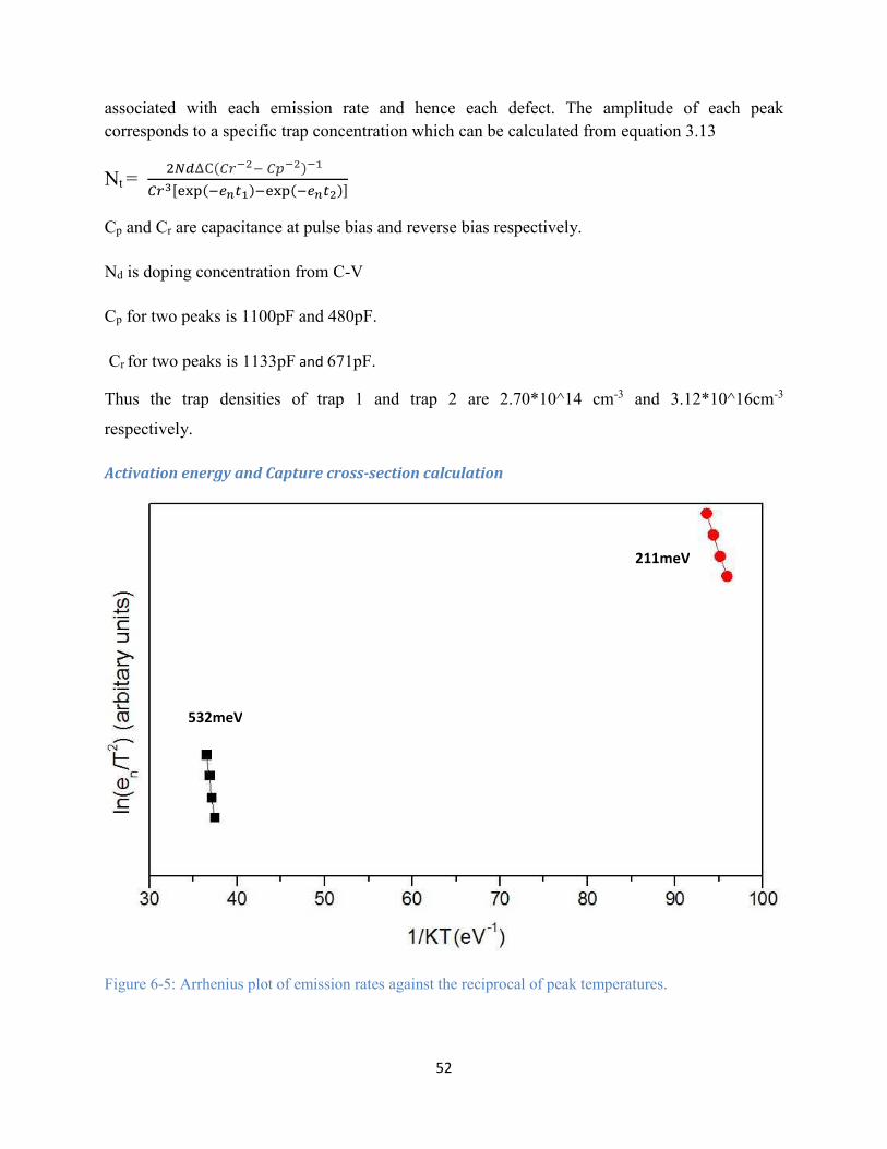
Third layer: Gold is deposited over contacts as a protective layer. This layer prevents any
changes in the properties of the Schottky diode and contacts ripping off when the device is being
wire bonded. This is because the wire bonder uses heat and ultrasonic energy to form a bond
which may damage the Schottky diode. Generally a 5nm Au layer is sputtered on the contacts
using a CVC 610 DC magnetron sputtering station.
Figure 5-26: Au sputtered layer on contacts
Page 53
45
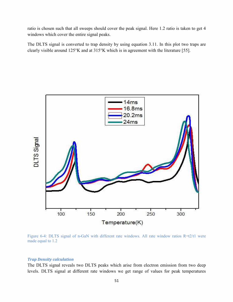
Chapter 6: DLTS Setup and DLTS Study of GaN
6.1Overview
This chapter deals with the instrumentation and setup in DLTS study. Technically, Deep level
transient spectroscopy is a C-V measurement over a temperature range. All the hardware
equipment used in C-V measurements is used for DLTS along with the temperature variation and
controlling equipment. A cryo-refrigerator system is used to bring the temperature down to as
low as 15°K in an open loop manner. A temperature controller along with heater wire on the
refrigerator sample cold head is used to control the actual temperature of the cold head and
sample in the chamber. A pulse generator, capacitance meter and oscilloscope are used to apply
bias pulses and to measure capacitance across the Schottky diode respectively to analyze the
DLTS-signal.
Figure 6-1: Deep Level Transient Spectroscopy (DLTS) hardware system.
6.2 DLTS Hardware:
6.2.1 Refrigerator system:
The refrigerator used in this work is Model 22 CTI Cryodyne refrigerator, which is a closed
cycle helium refrigeration system. It uses helium gas from the helium compressor (cryogenics
8200) to attain low temperatures. High pressure helium gas from a compressor comes through a
supply gas line to the regenerator. The regenerator cools the incoming gas and finally the gas
exits the cold head through the exit gas line. Using helium adsorbed this system can go down to
10 °Kelvin.
Page 54
46
The space around the cold head is evacuated to thermally isolate the cold head from room
temperature. No moisture should form on the refrigerator while running, which ensures there is
vacuum and no leak in the system. Air is sucked out from the chamber with a vacuum pump. A
Leybold trivac vacuum pump is used for this purpose. It is capable of exerting 10-3 Torr pressure
which can be read on a vacuum gauge attached to the pump.
6.2.2 Temperature Controller
The temperature controller (TC) is used to maintain a particular temperature in the chamber.
The TC system has a sensor and heater wire to attain a specified temperature. The DRC 91C is
the TC used in this experiment. A sensor is mounted as close as possible to the sample package
and the cold head mount to reduce the error in actual temperature and measured temperature. The
DT-670C-CU-HT is a silicon diode sensor used for measuring the temperature of the cold head.
The temperature range of the silicon diode used is 1.4K to 500K. A heater wire is wound around
the cold head. The heater wire used is 32AWG nichrome heater wire, which is capable of
handling 50W power supplied from the temperature controller. After selection of set point, the
TC attains a particular temperature (Set point) in the chamber by parallel cooling and heating
effect. It measures the temperature of the cold head using the sensor and adjusts accordingly the
current to a heater or not based on this feedback signal.
6.2.3 Pulse Signal generator
The pulse generator’s main purpose is to supply the filling pulse to the Schottky diode. An
Agilent 33220A signal generator is used for generating bias pulses in this study. The Agilent
33220A is an arbitrary waveform generator which is free from periodic noise. Pulses with
different time period and voltage peaks can be generated. For this study, a pulse with 2Vp-p for
100μs is generated in a 1ms waveform.
6.2.4 Capacitance meter
A Boonton 7200 capacitance meter is used for measuring the capacitance of semiconductor
devices, which is capable of measuring capacitance in the order of pico Farads. It has a fast
response and a recovery time of less than 50μs after an overload condition. This capacitance
meter is connected across the Schottky diode to measure the capacitance transient. It has both
digital and analog capacitance output. Since DLTS measures transient capacitance, an analog
capacitance is output from the meter and is displayed on an oscilloscope for measuring change in
capacitance over different time windows. This output presents a calibrated, real time reference
voltage proportional to the capacitance of the semiconductor under test.
6.2.5 Oscilloscope
An HP 54602B Oscilloscope is used to view the input and output waveforms. Pulse bias input
and analog capacitance output display on an oscilloscope. The change in capacitance value is
easily measured between rate windows in this oscilloscope using cursors.
Page 55
47
6.2.6 Package and connectors:
The GaN sample is mounted on the cold head using a Small Outline Integrated Circuit (SOIC)
package. The package is thermally conductive as the sample should be at the same temperature
of the cold head. The package is attached firmly to the cold head with silver paste and
mechanical clamp setup. The GaN sample is firmly attached to the package with silver paste.
Schottky diode contacts are wire bonded to the package.
36AWG Quad twist wires are used as signaling wires through which bias voltage is applied and
capacitance values are measured. Twisted pair wires are used to reduce noise due to
electromagnetic interference in wires which is cancelled out by comparing signals from both
ends.
6.3 Experimental Work
6.3.1 Schottky diode on GaN
Schottky diode has both ohmic and Schottky contacts for DLTS measurements. Electron beam
deposited Ni/Au dot contacts, act as Schottky and Ti/Al/Ti/Au rings annealed act as ohmic on n-
type. The dots range from 100 to 400μm in radius, while the surrounding inner ring radius is 50
μm greater than the dot radius, to reduce the series resistance as much as possible. The
fabrication of the Schottky diode is discussed in chapter 5 in detail.
6.3.2 CV study on GaN
Initially C-V measurements are taken with varying voltage across the Schottky diode and reading
capacitance values. From C-V results Nb, the background concentration of the GaN sample is
calculated which is explained in section 3.3.
Page 56
48
Figure 27-31: Capacitance-Voltage measurement process setup
i. CV analysis on n-GaN:
Shown in Figure 6-32, is a plot of (1/C2) versus voltage of a n-GaN (1651) sample. The slope of
the curve (1/C2) versus voltage is used in equation 3.7 to determine Nd.
The slope of the curve is calculated using a linear fit between the marked points, which is
1.0275*1019.
Using equation, Nd = −2 XYZ3[U [9\Y , the donor concentration, Nd = -1.844*1017/cm-3.
Page 57
49
Figure 6-32: Capacitance-Voltage measurement on n-GaN
ii. CV analysis on p-GaN:
Shown in Figure 6-33, is a plot of (1/C2) versus voltage of a p-GaN (1652) sample. The slope of
curve (1/C2) versus voltage is used in equation 3.7 to determine Na.
The slope of the curve between the marked points is 1.53*1020.
Using equation, Na = 2 XYZ3[U [9\Y , the acceptor concentration, Na = 1.229*1016/cm-3.
Page 58
50
Figure 6-33: Capacitance-Voltage measurement on p-GaN
6.3.3 DLTS study on GaN
DLTS measurement involves analysis of junction capacitance following a bias pulse over a range
of temperature. Initially the vacuum pump valve is opened to pump down the chamber and fully
isolate it from the atmosphere. The helium compressor enables the cold head temperature to drop
to 15°K. The temperature controller maintains chamber temperature equal to the set point. Set
point is increased in intervals of 1°K starting from 25°K to 400°K. At each point of the interval,
with pulse generator is in the ON position, the change in capacitance is measured on an
oscilloscope. This is done for different rate windows which are selected based on the
requirement�cDc� = K�. The capacitance transients are converted into the DLTS-signal by
correlating them. The simplest DLTS correlation is the 2-point correlation, where the capacitance
is measured at two times t1 and t2 after the end of each filling pulse, and the difference between
these two values is displayed:
( ) )C(t-)C(ta DLTS 12=
The difference is divided with C0 (capacitance at steady state) to get the normalized values which
is discussed in 3.10 and plotted as a function of temperature gives DLTS signal. Rate window
Page 59
51
ratio is chosen such that all sweeps should cover the peak signal. Here 1.2 ratio is taken to get 4
windows which cover the entire signal peaks.
The DLTS signal is converted to trap density by using equation 3.11. In this plot two traps are
clearly visible around 125°K and at 315°K which is in agreement with the literature [55].
Figure 6-4: DLTS signal of n-GaN with different rate windows. All rate window ratios R=t2/t1 were
made equal to 1.2
Trap Density calculation
The DLTS signal reveals two DLTS peaks which arise from electron emission from two deep
levels. DLTS signal at different rate windows we get range of values for peak temperatures
Page 60
52
associated with each emission rate and hence each defect. The amplitude of each peak
corresponds to a specific trap concentration which can be calculated from equation 3.13
Nt = D#�ef�X^(Y� XC(Y�(l
X^]mnop�����l��nop�����Y�q
Cp and Cr are capacitance at pulse bias and reverse bias respectively.
Nd is doping concentration from C-V
Cp for two peaks is 1100pF and 480pF.
Cr for two peaks is 1133pF and 671pF.
Thus the trap densities of trap 1 and trap 2 are 2.70*10^14 cm-3 and 3.12*10^16cm-3
respectively.
Activation energy and Capture cross-section calculation
Figure 6-5: Arrhenius plot of emission rates against the reciprocal of peak temperatures.
532meV
211meV
Page 61
53
For each measurement the value of en = ln(�D���/ � is calculated for each trap observed. An
Arrhenius plot is plotted for values of ln (���Y) as a function of 1/KT. The plot can be seen in
figure 6-5, where Ea is the slope and ln (γ σ) is the y-intercept. It is found that 211meV and
532meV are the observed activation energies of the traps from the Arrhenius plot.
Conclusion and Future Work
The I-V measurement on Schottky diode shows it is almost an ideal diode. Capacitance-Voltage
results quantify the doping concentrations of n-GaN and p-GaN which are 1.844*1017/cm-3 and
1.229*1016/cm-3 respectively. Deep level traps in GaN effect the performance of LED and other
devices made out of the GaN. Deep Level Transient Spectroscopy (DLTS) characterizes GaN
grown by MOCVD, which reveals two traps in temperature range of 50°K to 400°K. These two
traps are commonly observed in n- GaN. The DLTS peak amplitude of trap E1 varies with filling
pulse time tp. This is due to the line defect formed by dislocations. On the other hand, E2 is
dominant peak and the peak increases with increase in Si doping concentration, which induces
point defects. The traps with thermal activation energies 211meV and 532meV were observed.
However, DLTS for p-GaN is difficult to analyze. The specific contact resistivity of n-GaN
(5.43E-5 Ohm.cm2) is less compared to p-GaN (1.34E-2 Ohm.cm2). The limitation in maximum
concentration of Mg that can be doped during growth and atoms ionized at room temperature
make it difficult to fabricate a tunneling ohmic contact to p-GaN, which caused the DLTS signal
distorted.
With cooler growth temperatures surface stress, forming dislocation densities can be reduced
which decrease the E1 defect levels. With the decrease in Si concentration during doping, E2
trap densities can be minimized in n-GaN.
Page 62
54
References
[1]Novel metalorganic chemical vapor deposition system for GaN growth Shuji
Nakamura,Tokushima 774, Japan.
[2]. H.P. Maruska and J.J. Tietjen, Appl. Phys. Lett., 15 (1969) 327
[3] History of Gallium–Nitride-Based Light-Emitting Diodes for Illumination by Shuji
Nakamura and Michael R. Krames, Senior Member IEEE
[4] S. Nakamura, T. Mukai, and M. Senoh, ‘‘Candera-class high-brightness InGaN/AlgaN
double-heterostructure blue-light-emitting diodes,’’ 1687–1689, 1994.
[5] M. J. Cich, R. I. Aldaz, A. ‘‘Bulk GaN based violet light-emitting diodes with high efficiency
at very high current density,’’ Appl. Phys. Lett., vol. 101, 2012, 223509.
[6] Lee Stauffer, Keithley Instruments, Inc, “Fundamentals of Semiconductor C-V
Measurements”
[7] http://en.wikipedia.org/wiki/P%E2%80%93n_junction
[8] Solid state electronic devices by Streetman
[9] H. Hellmann, MRS Internet J. Nitride Semicond. Res. 1, 33 (1996)
[10] E. Zavoiski, J. Phys. USSR 9, 211, 245, 447 (1945).
[11] H.H. Woodbury and G.W. Ludwig, Phys. Rev. 117, 102 (1960).
[12] W. Low, Paramagnetic resonance in solids. In: F. Seitz, D. Turnbull (Eds.), Solid Satate
Phys., Suppl. 2, 1960.
[13] G.W. Ludwig and H.H. Woodbury, Solid State Phys. 13, 223 (1962).
[14] J.W Allen, Semicond. Sci. Technol. 10, 1049 (1995).
[15] B.C. Cavenett, Adv. Phys. 30, 475 (1981)
Page 63
55
[16] N. Nakamura and G. Fasol, The Blue Laser Diode, Springer-Verlag, Berlin, 1997.
[17] S.C. Binari, W. Kruppa, H.B. Dietrich, G. Kelner, A.E. Wickenden and J.A. Freitas Jr.,
Solid State Electron. 41, 1549 (1997).
[18] RB. Klein, J.A. Freitas Jr., S.C. Binari and A.E. Wickenden, Appl. Phys. Lett. 75, 4016
(1999).
[19] D. V. Lang, Bell Laboratories, Murray Hill, New Jersey 07974
Deep-level transient spectroscopy: A new method to characterize traps in semiconductors
[20] N. M. Johnson, Mater. Res. Sot. Symp. Proc. 69, 7.5 (1986)
[21] H.P. Maruska and J.J. Teitjen, Appl. Phys. Lett. 15, 367 (1969).
[22] H. Amano, N. Sawaki, I. Akasaki and Y. Toyoda, Appl. Phys. Lett. 48, 353 (1986).
[23] I. Akasaki, H. Amano, Y. Koide, K. Hiramnatsu and N. Sawaki, J. Crystal Growth 98, 209
(1989)
[24] F.A. Ponce, MRS Bull. 22, 51 (1997).
[25] Z. Liliental-Weber, C. Kisielowski, S. Ruvimov, Y. Chen and J. Washburn, J. Electron.
Mat. 25, 1545 (1996).
[26] X.H. Wu, L.M. Brown, D. Kapolnek and S., Keller et al., J. Appl. Phys. 80, 3228 (1996).
[27] Z. Liliental-Weber, S. Ruvimov, T. Suski, J.W. Ager III, W Swider, J. Washburn, H.
Amano, I. Akasaki and W Imler, Mat. Res. Soc. Symp. Proc. 423, 487 (1996).
[28] Z. Liliental-Weber, J. Washburn, K. Pakula and J. Baranowski, Microsc. Microanal (1997).
[29] C. Kisielowski, J. Kriiger, S. Ruvimov, R.F. Davis, Phys. Rev. B 54, 17745 (1996).
[30] H. Amano, N. Sawasaki, I. Akasaki and Y. Toyoda, Appl. Phys. Lett. 48, 353 (1986)
[32] "Schottky barrier", Wikipedia, The Free Encylopedia. 20.April 2006
Page 64
56
[33] Miron J. Cristea ‘Politehnica’ University of Bucharest, 313 Spl. Independentei, Bucharest
Capacitance-voltage profiling techniques for characterization of semiconductor materials and
devices
[34] O. Breitenstein 2003, DLTS manual
[35] 23 N.M. Johnson, Opt. Eng. 25, 698 (1986)
[36, 37] Sula technologies, Deep Level Transient Spectroscopy.
[38] Jian Sun and Jürgen Kosel, Finite-Element Modelling and Analysis of Hall Effect and
Extraordinary Magnetoresistance Effect
[39] E. Ramsden, 2006Hall-effect Sensors: Theory and Applications. Oxford: Newnes.
[40] T. L. Estle, S. K. Estreicher, D. S. Marynick: Hyp. Inter. 32, 637 (1986) 14,16
[41] T. L. Estle, S. K. Estreicher, D. S. Marynick: Phys. Rev. Lett. 58, 1547 (1987)
[42] A. M. Stoneham: Theory of Defects in Solids (Clarendon, Oxford 1985
[43] [18] Juza R, Hahn H. Zeitschrift für Anorganische und Allgemeine Chemie, 1938;234:282
1940;244:133.
[44] Grimmeiss H, Koelmans ZH. Nature 1959;14a:264
[45] Nakamura S, Pearton S, Fasol G. The Blue Laser Diode: The Complete Story 2000
[46] L.Liu, J.H. Edgar , Substrates for a gallium nitride epitaxy.
[47] "Wurtzite polyhedra" by Solid State - Own work. Licensed under Public domain via
Wikimedia Commons.
[48] Shockley W, Read WT. Statistics of the Recombinations of Holes and Electrons. Physical
Review [Internet]. 1952 ;87:835. http://link.aps.org/doi/10.1103/PhysRev.87.835
[49] http://www.asdn.net/asdn/physics/traps.shtml
[50] Dieter K. Schroder, Semiconductor Material and Device Characterization, Wiley Inter
Science.
[51] Deep Level transient spectroscopy, university of Melbourne, may 2005.
Page 65
57
[52] N.M. Johnson, Opt. Eng. 25, 698 (1986)
[53] Fong kwong Yam, Li Li low, GaN: An overview of structural defects, Universiti sains
Malaysia.
[54] Pallab Bhattacharya, Semiconductor optoelectronic devices, University of Michigan,Ann
Arbor.
[55] Hadis Morkoc, Handbook of Nitride semiconductors and devices, WILEY-VCH.
[56] Z-Q. Fang et al., Appl. Phys. Lett. 78, 332 (2001).
[57] H. K. Cho, C. S. Kim, and C.-H. Hong, Semiconductor Physics Research Center(2003).
[58] www.iue.tuwien.ac.at/phd/ayalew/node56.html
[59] http://ece-www.colorado.edu/~bart/book Van Zeghbroeck, 2011
[60] Heime, K., InGaAs Field-Effect Transistors, Research Studies Press LTD, England (1989)
[61] Christianson, K. A., Moglestue, C., and Anderson, W. T., Solid-State Elec., 38:1623 (1995)
[62] Pallab Bhattacharya, Semiconductor optoelectronic devices. Prentice-Hall, 1994.
[63] Rhoderick,E.H. Metal-Semiconductor contacts. Clarendon Press, Oxford, 1978.
[64] J. Bardeen,"Surface States and Rectification at a Metal Semiconductor Contact,"(1947).
[65] D. A. Neamen, Semiconductor physics & devices. 2nd Ed. (McGraw-Hill, 1997).
[66] Saraswat, Meatl semiconductor ohmic contacts, Stanford. f
[67] Metal-Semiconductor Contacts, Institute of EECS, Berkeley.
[68] Ben G. Streetman, Solid State Electronic Devices.
[69] L.L Smith, S.W.King, “Cleaning of GaN surfaces” Davis materials research center NCSU.
[70] J. S. Kwak, K. Y. Lee, J. Y. Han, J. Cho Appl. Phys. Lett. 79 (20) 2001
[71] Ja-Soon Jang, Kyung- Hyun Park, Hong-Kyu Jang, J. Vac. Sci. Technol. B. 16 (6), 1998
Page 66
58
[72] R. Williams,Modern GaAs Processing Techniques (Norwood, MA: Artech House, 1990).
[73] E. Yablonovitch, D.L. Allara, C.C. Chang, T. Gmitter Phys. Rev. Lett. 57, 249 (1986)
[74] http://www.ece.gatech.edu/research/labs/vc/theory/photolith.html
[75] http://en.wikipedia.org/wiki/Photolithography
[76] W. Götz, N. M. Johnson, J. Walker, D. P. Bour and R. A. Street Activation of acceptors in
Mg‐doped GaN grown by metalorganic chemical vapor deposition
[77] B. A. Hull, S. E. Mohney,” Influence of oxygen on the activation of p-type GaN”
[78] http://www.ece.gatech.edu/research/labs/vc/theory/photolith.html
[79] Cornell nano scale science and technology facility.
http://www.cnf.cornell.edu/cnf_process_photo_resists.html#manual spin
[80] R. Behrisch (ed.) (1981). Sputtering by Particle bombardment:. Springer, Berlin
[81] Vamsi Krishna kumbham , “Synthesis and Characterization of electrodes for III-Nitride
Resonant Cavity Light Emitting Diode Applications”.