Characterization of Electrostatic Potential and Trapped Charge in Semiconductor Nanostructures using Off-Axis Electron Holography by Zhaofeng Gan A Dissertation Presented in Partial Fulfillment of the Requirements for the Degree Doctor of Philosophy Approved April 2015 by the Graduate Supervisory Committee: Martha R. McCartney, Co-Chair David J. Smith, Co-Chair Jeffery Drucker Peter A. Bennett ARIZONA STATE UNIVERSITY May 2015
Transcript
Characterization of Electrostatic Potential and Trapped Charge in
Semiconductor Nanostructures using Off-Axis Electron Holography
by
Zhaofeng Gan
A Dissertation Presented in Partial Fulfillment of the Requirements for the Degree
Doctor of Philosophy
Approved April 2015 by the Graduate Supervisory Committee:
Martha R. McCartney, Co-Chair
David J. Smith, Co-Chair Jeffery Drucker Peter A. Bennett
ARIZONA STATE UNIVERSITY
May 2015
ABSTRACT
Off-axis electron holography (EH) has been used to characterize electrostatic
potential, active dopant concentrations and charge distribution in semiconductor
nanostructures, including ZnO nanowires (NWs) and thin films, ZnTe thin films, Si NWs
with axial p-n junctions, Si-Ge axial heterojunction NWs, and Ge/LixGe core/shell NW.
The mean inner potential (MIP) and inelastic mean free path (IMFP) of ZnO NWs
have been measured to be 15.3V±0.2V and 55±3nm, respectively, for 200keV electrons.
These values were then used to characterize the thickness of a ZnO nano-sheet and gave
consistent values. The MIP and IMFP for ZnTe thin films were measured to be 13.7±0.6V
and 46±2nm, respectively, for 200keV electrons. A thin film expected to have a p-n
junction was studied, but no signal due to the junction was observed. The importance of
dynamical effects was systematically studied using Bloch wave simulations.
The built-in potentials in Si NWs across the doped p-n junction and the Schottky
junction due to Au catalyst were measured to be 1.0±0.3V and 0.5±0.3V, respectively.
Simulations indicated that the dopant concentrations were ~1019cm-3 for donors and ~1017
cm-3 for acceptors. The effects of positively charged Au catalyst, a possible n+-n--p junction
transition region and possible surface charge, were also systematically studied using
simulations.
Si-Ge heterojunction NWs were studied. Dopant concentrations were extracted by
atom probe tomography. The built-in potential offset was measured to be 0.4±0.2V, with
the Ge side lower. Comparisons with simulations indicated that Ga present in the Si region
was only partially activated. In situ EH biasing experiments combined with simulations
i
indicated the B dopant in Ge was mostly activated but not the P dopant in Si. I-V
characteristic curves were measured and explained using simulations.
The Ge/LixGe core/shell structure was studied during lithiation. The MIP for LixGe
decreased with time due to increased Li content. A model was proposed to explain the
lower measured Ge potential, and the trapped electron density in Ge core was calculated to
be 3×10¹⁸ electrons/cm3. The Li amount during lithiation was also calculated using MIP
and volume ratio, indicating that it was lower than the fully lithiated phase.
ii
DEDICATION
To my parents
iii
ACKNOWLEDGMENTS
First of all, I would like to express my deepest gratitude to my supervisors,
Professor Martha R. McCartney and Regents’ Professor David J. Smith, for their support,
guidance and encouragement that made everything I achieved possible during my PhD
study. Their enthusiasm, meticulous attitudes, precise insight and great patience in doing
research and teaching students have deeply impressed me and educated me as good
characteristics for my future career.
I would like to thank Professors Jeff Drucker and Peter Bennett for helpful
suggestions and for serving on my dissertation committee. I am grateful for the use of
facilities in the John M. Cowley Center for High Resolution Electron Microscopy. Special
thanks to Karl Weiss, Dr. Zhenquan Liu and Dr. Toshihiro Aoki for their technical support
and assistance throughout my research. The financial support from US Department of
Energy (Grand No. DE-FG02-04ER46168) is gratefully acknowledged.
I also would like to express my deep appreciation to Dr. S. Tom Picraux, Dr.
Jinkyoung Yoo of Los Alamos National Lab, Dr. Daniel E. Perea, Dr. Chongmin Wang of
Pacific Northwest National Lab, and Professor Hongbin Yu, Yonghang Zhang of Arizona
State University for their collaboration and for providing the samples characterized in this
dissertation.
Particular thanks to our research group members- Dr. Lin Zhou, Dr. Kai He, Dr.
Luying Li, Dr. Wenfeng Zhao, Dr. Lu Ouyang, Dr. Jaejin Kim, Dr. Michael Johnson, Dr.
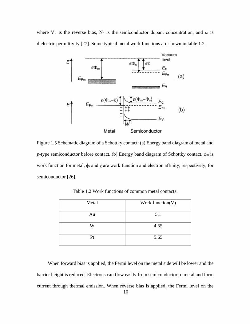
where VR is the reverse bias, Nd is the semiconductor dopant concentration, and εs is
dielectric permittivity [27]. Some typical metal work functions are shown in table 1.2.
Figure 1.5 Schematic diagram of a Schottky contact: (a) Energy band diagram of metal and
p-type semiconductor before contact. (b) Energy band diagram of Schottky contact. ϕm is
work function for metal, ϕs and χ are work function and electron affinity, respectively, for
semiconductor [26].
Table 1.2 Work functions of common metal contacts.
Metal Work function(V)
Au 5.1
W 4.55
Pt 5.65
When forward bias is applied, the Fermi level on the metal side will be lower and the
barrier height is reduced. Electrons can flow easily from semiconductor to metal and form
current through thermal emission. When reverse bias is applied, the Fermi level on the 10
metal side will be higher and the barrier height as well as the depletion region width are
increased. There is no current through the Schottky contact under this condition. Therefore,
the Schottky contact shows similar rectifying effect as the p-n junction, although the
current across the Schottky contact is mainly due to majority carriers [25].
1.2.2.2 Ohmic Contact
Figure 1.6 shows the schematic diagram of an ohmic contact between a metal and an
n-type semiconductor. The metal and p-type ohmic contact is similar and is not described
here. In this case, the Fermi level on the metal side is higher than for the semiconductor
and electrons flow from metal to semiconductor. Because of these extra electrons, the
semiconductor becomes more n-type and there are extra surface electrons at the metal-
semiconductor interface. As positive bias is applied to the metal, electrons flow easily to
the metal from the semiconductor. When negative bias is applied, electrons can also go
easily through the barrier and flow to the semiconductor. Therefore, the current through
the contact is proportional to the voltage [25].
11
Figure 1.6 Schematic diagram of a metal-semiconductor ohmic contact: (a) Band structure
of metal and semiconductor before contact. (b) Band structure of metal-semiconductor
ohmic contact at thermal equilibrium. (c) Band structure of metal-semiconductor ohmic
contact with positive bias on metal. (d) Band structure of metal-semiconductor ohmic
contact with negative bias on metal [25].
Another type of metal-semiconductor contact is based on a tunneling effect. As
shown in Figure 1.7, due to heavy dopant concentrations in the n-type semiconductor, the
depletion region near the semiconductor surface is very narrow and electrons can easily
tunnel through the barrier, forming an ohmic contact [25].
12
Figure 1.7 Schematic energy band structure diagram of metal and heavily doped n-type
semiconductor [25].
1.2.3 Heterojunction
The heterojunction is formed by connecting two semiconductors of different energy
band gaps. The energy band alignment (both of conduction and valence band) is usually
not continuous across the heterojunction interface, due to the differences in energy band
gap, electron affinity and Fermi level. Moreover, the lattice mismatch between the two
materials must be small to avoid interface strain, defects and trap states. The heterojunction
can also be realized by using pseudomorphic (strain layer) structures. The lattice constants
and energy band gaps for common semiconductors are shown in figure 1.8. The main
advantages of heterojunctions are controlling the energy barriers and potential variations
at the interface in order to control the charge carrier transport, and to confine the optical
radiation, which is important for optoelectronic devices [25,26].
13
Figure 1.8 Energy band gaps and lattice constants for Si, Ge and several III-V compound
semiconductors [2].
There are three different types of energy band alignment at heterojunctions, as shown
in Figure 1.9. Figure 1.9a is usually referred to as type I or straddling band alignment,
where one of the materials has lower Ec and higher Ev, compared to the other material, so
that electrons and holes are confined in the same material. Figure 1.9b is usually referred
to as type II or staggered band alignment, where the locations of lower Ec and higher Ev
are displaced so that the electrons and holes are confined in different materials. Figure 1.9c
is usually referred to as type III or broken-gap band alignment. Its conduction band
overlaps with the valence band at the interface. Si-Ge has type II band alignment [25].
Figure 1.9 Schematic energy band diagrams for different types of heterojunctions [25]. 14
Figure 1.10 shows a schematic energy band diagram for alignment at the
heterojunction. There are several theories of band alignment for heterojunctions and the
major issue is whether the band-gap discontinuities are determined by the bulk properties
or by the interface properties. The electron-affinity model suggests that by using the
vacuum level as the reference, the conduction-band discontinuity ∆𝐸𝐸𝑐𝑐 at the interface can
be calculated from the difference in electron affinities of the two materials.
∆𝐸𝐸𝑐𝑐 = 𝑒𝑒(𝜒𝜒1 − 𝜒𝜒2) (1.4)
The discontinuity at the valence band ∆𝐸𝐸𝑣𝑣 can be calculated by [2,25]:
∆𝐸𝐸𝑣𝑣 = �𝑒𝑒𝜒𝜒2 + 𝐸𝐸𝑔𝑔2� − (𝑒𝑒𝜒𝜒1 + 𝐸𝐸𝑔𝑔1) (1.5)
Moreover, when the two different materials are in contact, the Fermi levels line up to
restore thermal equilibrium. In this case, the electrons (holes) in n-type (p-type) material
diffuse into the other side, forming a depletion region at the interface. The resultant electric
field will bend the band structure in n-type (p-type) material upward (downward), forming
the discontinuity at the interface. The built-in potential 𝑉𝑉𝑏𝑏𝑖𝑖 can then be described by [26]:
𝑒𝑒𝑉𝑉𝑏𝑏𝑖𝑖 = 𝐸𝐸𝑔𝑔1 + ∆𝐸𝐸𝑐𝑐 − ∆𝐸𝐸𝐹𝐹1 − ∆𝐸𝐸𝐹𝐹2 (1.6)
15
Figure 1.10 Schematic energy band diagram for heterojunctions before and after contact
[26].
1.3 Growth of Semiconductor Nanostructures
1.3.1 Epitaxial Growth Techniques
Semiconductor nanowires can be grown by a wide variety of epitaxial growth
techniques, which include chemical-vapor deposition (CVD) and molecular-beam expitaxy
(MBE).
CVD is a technique that enables thin film growth on a suitable substrate material
using chemical reaction of vapor-phase precursors to form the desired deposit. The
substrate is usually used as the seed crystal, and because it uses a chemical reaction as the
deposit-forming mechanism, the growth temperature can be much lower relative to the thin
film melting point. The conventional CVD process can be described as follows: (a) the
16
precursors are evaporated and transported from the bulk gas region into the reactor chamber,
using carrier gas; (b) reactive intermediates and gaseous by-products are produced from
gas-phase precursor reactions; (c) reactants are transported and adsorbed by the substrate
surface; (d) reactants diffuse to the growth site, and the thin film is grown by surface
nucleation and chemical reactions; (e) the remaining decomposition materials are desorbed
and transported out of the chamber [1,28]. The Si, Ge, Si/Ge heterojunction NWs
characterized in Chapters 4, 5 and 6 were gown using a cold-wall CVD reactor using the
VLS growth mechanism described below.
MBE is an epitaxial growth technique that uses the interaction of molecular or atomic
beams on a heated crystal substrate surface under ultrahigh-vacuum condition. The growth
rate in MBE is usually low (~1 monolayer per second) and this technique thus enables
precise control of film thicknesses, compositions, dopants, and morphology. The absence
of carrier gas and ultrahigh-vacuum can help to reduce the level of impurities during
growth. Moreover, reflection-high-energy electron diffraction can be used for monitoring
the crystal layer growth for better structure and thickness control. The MBE growth process
can be described as follows: (a) solid-source atoms or homo-atomic molecules of the
growth material in separate quasi-Knudsen diffusion cells are evaporated, transported and
condensed on the heated crystal substrate surface. (b) atoms diffuse on the surface and react
with other atoms to form the epitaxial layer [29,30]. The ZnTe thin film characterized in
Chapter 3 was grown using the MBE method.
1.3.2 Nanowire Growth
Three different methods are most commonly used for growing freestanding NWs
originating from the substrate surface: these are vapor-liquid-solid (VLS) [20,31-33],
17
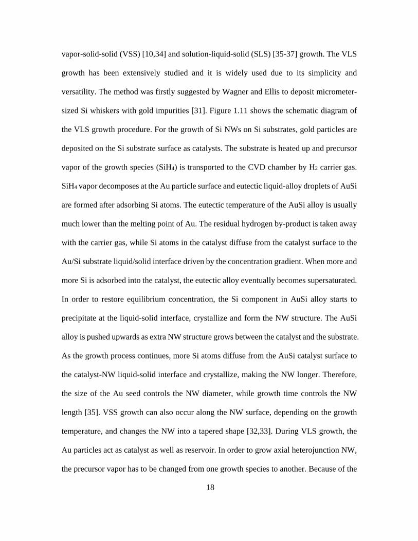
vapor-solid-solid (VSS) [10,34] and solution-liquid-solid (SLS) [35-37] growth. The VLS
growth has been extensively studied and it is widely used due to its simplicity and
versatility. The method was firstly suggested by Wagner and Ellis to deposit micrometer-
sized Si whiskers with gold impurities [31]. Figure 1.11 shows the schematic diagram of
the VLS growth procedure. For the growth of Si NWs on Si substrates, gold particles are
deposited on the Si substrate surface as catalysts. The substrate is heated up and precursor
vapor of the growth species (SiH4) is transported to the CVD chamber by H2 carrier gas.
SiH4 vapor decomposes at the Au particle surface and eutectic liquid-alloy droplets of AuSi
are formed after adsorbing Si atoms. The eutectic temperature of the AuSi alloy is usually
much lower than the melting point of Au. The residual hydrogen by-product is taken away
with the carrier gas, while Si atoms in the catalyst diffuse from the catalyst surface to the
Au/Si substrate liquid/solid interface driven by the concentration gradient. When more and
more Si is adsorbed into the catalyst, the eutectic alloy eventually becomes supersaturated.
In order to restore equilibrium concentration, the Si component in AuSi alloy starts to
precipitate at the liquid-solid interface, crystallize and form the NW structure. The AuSi
alloy is pushed upwards as extra NW structure grows between the catalyst and the substrate.
As the growth process continues, more Si atoms diffuse from the AuSi catalyst surface to
the catalyst-NW liquid-solid interface and crystallize, making the NW longer. Therefore,
the size of the Au seed controls the NW diameter, while growth time controls the NW
length [35]. VSS growth can also occur along the NW surface, depending on the growth
temperature, and changes the NW into a tapered shape [32,33]. During VLS growth, the
Au particles act as catalyst as well as reservoir. In order to grow axial heterojunction NW,
the precursor vapor has to be changed from one growth species to another. Because of the
18
residue of previous species in the catalyst, there is a transition region at the heterojunction
interface until the residue has all precipitated. The transition length is typically about the
same size as the NW diameter, as the volume of catalyst is proportional to R3 and the
diffusion interface area between liquid catalyst and solid NW is proportional to R2, where
R is the NW radius. Different metal catalysts together with the VSS method can thus be
used to lower solubility in the catalyst to reduce the width of transition region [10,20,38].
Figure 1.11 Schematic diagram of VLS NW growth [39].
1.4 Outline of Dissertation
In this dissertation research, the technique of off-axis electron holography has been
used to study a range of common semiconductors, including NW homojunctions and
heterojunctions. The technique was first used to measure the mean inner potentials (MIPs)
and inelastic mean free paths (IMFPs) for ZnO NW and ZnTe thin films. Characterization
of the electrostatic potential across Si NW with p-n junction, Au-Si Schottky junction in Si
19
NW, Si-Ge axial heterojunction NW, as well as Ge/LixGe core/shell NW structure were
also performed using this technique and compared with SilvacoTM device simulation and/or
Poisson equation calculation to determine the active dopant concentrations and trapped
charges in the nanostructures. Transmission electron microscopy (TEM), scanning
transmission electron microscopy (STEM) and electron-energy-loss spectrum (EELS)
technique were also used to characterize the morphology and structure of the
nanostructures, while atom probe tomography (APT) was used to determine the total
dopant concentrations and distributions in Si-Ge axial heterojunction NWs.
In Chapter 2, the background, theory and experiment setup for off-axis electron
holography are briefly described. An outline procedure for electron hologram
reconstruction is discussed, followed by reconstructed phase and thickness images
interpretation, definition and calculation of MIPs. The basis of EELS and high-angle
annular-dark-field imaging (HAADF) are also briefly discussed. Finally, the sample
preparation methods used in this thesis are described.
In Chapter 3, the morphology of ZnO NWs characterized using TEM is described.
The MIP and IMFP are measured using off-axis electron holography and applied to ZnO
thin films for the measurement of thickness. MIP and IMFP of ZnTe thin films are also
measured by combining off-axis electron holography and CBED thickness measurements.
The dynamic effects due to tilting and thickness are systematically studied for ZnTe thin
film by using simulations. Electrostatic potential across p-n junction in ZnTe thin film is
then measured using electron holography.
In Chapter 4, measurement of electrostatic potential across p-n junction and Schottky
junction in Si NW is performed using off axis electron holography. The built-in potential
20
is then extracted and compared with SilvacoTM simulations to determine the active dopant
concentrations. The influence of surface charge, transition region length and charging in
the Au catalyst particle are systematically studied by comparing experiment with
simulation results.
In Chapter 5, TEM and STEM HAADF are used to characterize the Si-Ge axial
heterojunction NW interface, and geometry phase analysis is performed based on HAADF
images. Characterization of electrostatic potential across Si-Ge axial heterojunction NWs
with/without in situ biasing using off-axis electron holography is presented. APT is also
performed to measure the total dopant concentrations and distributions. The SilvacoTM
simulations with/without biasing are compared with holography and APT results to
determine the active dopant amounts in Si-Ge NW.
In Chapter 6, the lithiation of Ge NWs to form Ge/LixGe core/shell structure is
outlined. The core/shell structure was characterized using TEM, STEM and EELS.
Electron holography experiments were then performed on the core/shell structure during
the lithiation process to measure the electrostatic potential. The measured potential was
compared with Poisson equation calculation to determine the amount of trapped charge in
the core/shell structure.
In Chapter 7, the important results and conclusions in the thesis are summarized, and
possible topics for further investigation are briefly described.
21
References
[1] S. M. Sze, Semiconductor devices, physics and technology, 2nd ed. Wiley, New York, (2002).
[2] S. M. Sze, Physics of semiconductor devices, 2nd ed. Wiley, New York, (1981).
[3] M. Faraday, Experimental researches in electricity. R. and J.E. Taylor, London, (1839).
[4] G. E. Moore, Proceedings of the IEEE 86 82 (1998).
[5] International Technology Roadmap for Semiconductors 2013, available online at http://www.itrs.net.
[6] R. Agarwal, Small 4 1872 (2008).
[7] Y. Wu, Y. Cui, L. Huynh, C. J. Barrelet, D. C. Bell, and C. M. Lieber, Nano letters 4 433 (2004).
[8] W. Lu, P. Xie, and C. M. Lieber, IEEE Transactions on Electron Devices 55 2859 (2008).
[9] W. Lu, J. Xiang, B. P. Timko, Y. Wu, and C. M. Lieber, Proc. Nat. Acad. Sci. 102 10046 (2005).
[10] C. Y. Wen, M. C. Reuter, J. Bruley, J. Tersoff, S. Kodambaka, E. A. Stach, and F. M. Ross, Science 326 1247 (2009).
[11] V. Schmidt, H. Riel, S. Senz, S. Karg, W. Riess, and U. Gosele, Small 2 85 (2006).
[12] J. Goldberger, A. I. Hochbaum, R. Fan, and P. Yang, Nano letters 6 973 (2006).
[13] J. Xiang, W. Lu, Y. Hu, Y. Wu, H. Yan, and C. M. Lieber, Nature 441 489 (2006).
[14] Y. Hu, H. O. Churchill, D. J. Reilly, J. Xiang, C. M. Lieber, and C. M. Marcus, Nature nanotechnology 2 622 (2007).
[15] I. Kimukin, M. S. Islam, and R. S. Williams, Nanotechnology 17 S240 (2006).
[16] Y. Cui, Q. Wei, H. Park, and C. M. Lieber, Science 293 1289 (2001).
[17] L. J. Lauhon, M. S. Gudiksen, C. L. Wang, and C. M. Lieber, Nature 420 57 (2002).
[18] O. Hayden, A. B. Greytak, and D. C. Bell, Advanced Materials 17 701 (2005).
22
[19] F. Qian, Y. Li, S. Gradecak, D. L. Wang, C. J. Barrelet, and C. M. Lieber, Nano letters 4 1975 (2004).
[20] D. E. Perea, N. Li, R. M. Dickerson, A. Misra, and S. T. Picraux, Nano letters 11 3117 (2011).
[21] L. Li, D. J. Smith, E. Dailey, P. Madras, J. Drucker, and M. R. McCartney, Nano letters 11 493 (2011).
[22] L. Chen, W. Y. Fung, and W. Lu, Nano letters 13 5521 (2013).
[23] U. K. Mishra, J. Singh, Semiconductor device physics and design. Springer, Dordrecht, The Netherlands, (2008).
[24] S. Dimitrijev, Understanding semiconductor devices. Oxford University Press, New York, (2000).
[25] D. A. Neamen, Semiconductor physics and devices : basic principles, 2nd ed. Irwin, Chicago, (1997).
[26] B. G. Yacobi, Semiconductor materials : an introduction to basic principles. Kluwer Academic/Plenum Publishers, New York, (2003).
[27] D. A. Neamen, Semiconductor physics and devices : basic principles, 3rd ed. McGraw-Hill Higher Education, London, (2003).
[28] A. C. Jones, M. L. Hitchman, and Knovel (Firm), Chemical vapour deposition precursors, processes and applications. Royal Society of Chemistry, Cambridge, UK, (2009).
[29] J. Y. Tsao, Materials fundamentals of molecular beam epitaxy. Academic Press, Boston, (1993).
[30] M. A. Herman and H. Sitter, Molecular beam epitaxy : fundamentals and current status, 2nd, rev. and updated ed. Springer, New York, (1996).
[31] R. S. Wagner and W. C. Ellis, Applied Physics Letters 4 89 (1964).
[32] J. W. Dailey, J. Taraci, T. Clement, D. J. Smith, J. Drucker, and S. T. Picraux, J Appl Phys 96 7556 (2004).
[33] S. A. Dayeh, J. Wang, N. Li, J. Y. Huang, A. V. Gin, and S. T. Picraux, Nano letters 11 4200 (2011).
[34] Y.-C. Chou, C.-Y. Wen, M. C. Reuter, D. Su, E. A. Stach, and F. M. Ross, ACS Nano 6 6407 (2012).
23
[35] V. Schmidt, J. V. Wittemann, S. Senz, and U. Gösele, Advanced Materials 21 2681 (2009).
[36] M.-S. Kim and Y.-M. Sung, Chem Mater 25 4156 (2013).
[37] A. T. Heitsch, D. D. Fanfair, H.-Y. Tuan, and B. A. Korgel, J Am Chem Soc 130 5436 (2008).
[38] N. Li, T. Y. Tan, and U. Gösele, Applied Physics A 90 591 (2008).
[39] G.-C. Yi, Semiconductor Nanostructures for Optoelectronic Devices Processing, Characterization and Applications, Springer, Heidelberg, (2012).
24
CHAPTER 2
EXPERIMENTAL DETAILS
This chapter begins by providing some background and basic theory of off-axis
electron holography. The procedures used for hologram reconstruction are then described,
followed by details of reconstructed phase and thickness image interpretation, definition
and calculation of mean inner potential (MIP), and the experimental setup used for
recording electron holograms. The basis of electron-energy-loss spectroscopy (EELS) and
high-angle annular-dark-field (HAADF) imaging are also briefly discussed. Finally, the
sample preparation methods used for the research of this dissertation are illustrated.
2.1 Off-Axis Electron Holography
2.1.1 Introduction
Transmission electron microscopy (TEM) has been widely used to characterize
nanostructured materials. However, conventional TEM only provides spatial intensity
information about the sample, while the phase and amplitude of the specimen exit-surface
electron wavefunction are unavailable. The phase and amplitude information are directly
related to the electrostatic and magnetic fields of the sample, which are very important for
characterization of semiconducting and magnetic materials.
Electron holography is an electron-interference technique that can provide amplitude
and phase information about the sample with nanoscale spatial resolution [1]. By
overlapping the exit-surface electron wave with a reference wave, an interference pattern
(hologram) is formed, which allows retrieval of phase and amplitude information. The
25
technique of in-line holography was first proposed by Gabor as a method for correcting the
spherical aberration of the objective lens, thus overcoming the interpretable resolution limit
[2]. Leith and Upatnieks proposed the off-axis electron holography geometry as a way to
solve the twin-image problem of in-line holography, by overlapping the sample wave with
the vacuum (reference) wave using an electrostatic biprism [3]. However, the approach
was not effectively realized experimentally until the development of the field emission gun
(FEG). The FEG provides a high brightness and highly coherent electron beam, which is
critical for hologram interference [4,5]. The holograms were originally recorded on
photographic plates with non-linear response and the hologram reconstruction was done
using a light optical system [6]. The emergence of digital recording devices, such as the
slow-scan charge-coupled-device (CCD), which provides linear response over a wide
dynamical range of electron counts, has enabled quantitative reconstruction of electron
hologram using computer processing [7].
Since the initial realization of electron holography, the technique has been
extensively developed and over twenty different approaches for the realization of electron
holography have been identified [8]. Among these approaches, off-axis electron
holography with operation in the TEM imaging mode is the most widely used and most
successful technique for obtaining sample phase and amplitude information [9]. This setup
has been exclusively used for the holography experiments described in this dissertation
research.
2.1.2 Theory and Hologram Reconstruction
A schematic diagram for off-axis electron holography with operation in the TEM
imaging mode is shown in Figure 2.1. Parallel (coherent) electron illumination from the
26
field emission gun (FEG) electron source is provided using the condenser lens system.
When the electron wave passes the specimen plane, it can be considered as being split into
two different parts. Part of the electron wave passes through the specimen, and will contain
phase and amplitude information that can be related to the sample. This object wave can
be described by the following equation:
𝛹𝛹(𝑟𝑟) = 𝐴𝐴(𝑟𝑟)exp (𝑖𝑖𝑖𝑖(𝑟𝑟)) (2.1)
where 𝐴𝐴(𝑟𝑟) and 𝑖𝑖(𝑟𝑟) are the amplitude and phase, respectively, at the two-dimensional
exit-surface of the sample. Part of the electron wave passes only through vacuum and
serves as the reference wave 𝛹𝛹𝑟𝑟(𝑟𝑟).
Figure 2.1 Schematic diagram showing the TEM components essential for the technique
of off-axis electron holography [9]. 27
When the electrostatic biprism below the specimen is positively charged, the object
and reference waves are deflected towards each other and overlap, eventually forming an
interference hologram in the final image plane where the CCD is located.
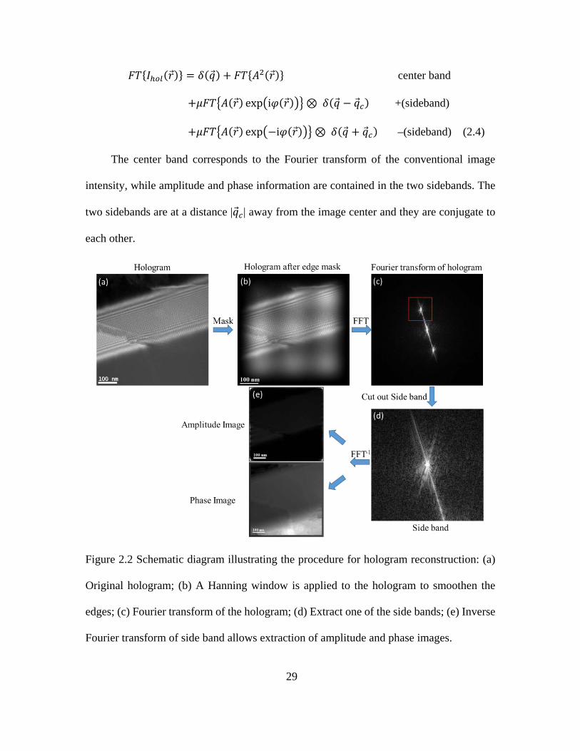
The hologram intensity 𝐼𝐼ℎ𝑜𝑜𝑜𝑜(𝑟𝑟) recorded by the CCD can be described by the
The dynamical effects were simulated and compared for several different crystalline
materials in the [011] projection, while the other parameters were kept constant. Values
taken off the zone and the Kikuchi band (Position 1), and at a minor Kikuchi band (Position
2), are shown in Table 3.4. The dynamical effects at these positions are still low and ~4%
of the phase due to MIP only. However, the phase change across the Kikuchi bands become
more visible when changing from Si to ZnTe, which indicates that the dynamical effects
become more important for heavier material. These results confirm that the dynamical
effects increase as the average atomic number increases. Therefore, for higher Z materials,
such as ZnTe, it is necessary to examine thinner areas to reduce diffraction effects.
3.2.4 Conclusions
The MIP of ZnTe was measured to be V0=13.7±0.6 V and the IMFP for 200keV
electron beam was measured to be λi=46±2 nm, using CBED and off-axis electron
holography. The measured MIP and IMFP were then used to investigate a ZnTe thin film
expected to have a pn junction. However, no change in signal due to built-in potential
across a junction was observed. The reasons might be: (a) Al dopants were not activated;
(b) the junction was beyond the field of view of the holography experiment. Dynamical
69
effects were systematically studied by using Bloch wave simulations. Choosing thinner
samples, avoiding low-index zone axes and careful tilting will all help to minimize
dynamical effects.
70
References
[1] Z. L. Wang, Journal of Physics: Condensed Matter 16 R829 (2004).
[2] M. H. Huang, S. Mao, H. Feick, H. Yan, Y. Wu, H. Kind, E. Weber, R. Russo, and P. Yang, Science 292 1897 (2001).
[3] B. Pal and M. Sharon, Mater Chem Phys 76 82 (2002).
[4] C. J. Lee, T. J. Lee, S. C. Lyu, Y. Zhang, H. Ruh, and H. J. Lee, Applied Physics Letters 81 3648 (2002).
[5] N. Ohashi, K. Kataoka, T. Ohgaki, T. Miyagi, H. Haneda, and K. Morinaga, Applied Physics Letters 83 4857 (2003).
[6] G. Sberveglieri, S. Groppelli, P. Nelli, A. Tintinelli, and G. Giunta, Sensors and Actuators B: Chemical 25 588 (1995).
[7] S. Baosheng, Y. Akira, and K. Makoto, Japanese Journal of Applied Physics 37 L206 (1998).
[8] J. J. Lee, Y. B. Kim, and Y. S. Yoon, Applied Surface Science 244 365 (2005).
[9] U. Özgür, Y. I. Alivov, C. Liu, A. Teke, M. A. Reshchikov, S. Doğan, V. Avrutin, S. J. Cho, and H. Morkoç, Journal of Applied Physics 98 041301 (2005).
[10] Y. Li, G. W. Meng, L. D. Zhang, and F. Phillipp, Applied Physics Letters 76 2011 (2000).
[11] Y. C. Kong, D. P. Yu, B. Zhang, W. Fang, and S. Q. Feng, Applied Physics Letters 78 407 (2001).
where CE is an electron-energy-dependent interaction constant with the value of 0.00728
rad V-1 nm-1 for 200-keV electrons, V0 is the mean inner potential (MIP) of the sample, Vbi
is the built-in potential and t is the diameter of NW served as the projected thickness.
In the case of a single p-n junction without bias, the built-in junction potential can be
calculated using the expression:
𝑉𝑉𝑏𝑏𝑖𝑖 = 𝑘𝑘×𝑘𝑘𝑒𝑒
× ln (𝑁𝑁𝐴𝐴×𝑁𝑁𝐷𝐷𝑛𝑛𝑖𝑖2 ) (4.2)
where k is Boltzmann’s constant, T is the absolute temperature, e is the electron charge, ni
is the intrinsic carrier concentration, and NA and ND are the acceptor and donor 75
concentrations [13]. Multiple junctions that are not far apart may cause the carriers to be
redistributed, such as for the case where a Schottky contact is located close to the p-n
junction. Furthermore, trap states at the native surface oxide/NW interface or within the
oxide itself will form a surface depletion region which further complicates transport
analysis [14,15]. Thus, more comprehensive simulations are necessary when charge
distributions and any changes in the sample geometry (eg. local NW thickness) are taken
into consideration. Careful comparison between simulation and experiment could then give
information about the distribution and concentration of the active dopants. In this study,
electron holography has been used to map the electrostatic field across the axial p-n
junction and the Au catalyst Schottky contact of a Si NW and estimates of the active dopant
concentrations have been extracted based on comparisons with simulations.
4.2 Experimental Details
Figure 4.1 Schematic diagram of the Si NW growth procedure: (a) Au particles were
deposited on Si substrate as catalysts; (b) n-type Si segment was grown using P as dopant;
(c) P source was switched off and a p-type Si segment was grown due to unintentional
dopant. 76
Figure 4.1 shows a schematic diagram of the Si NW growth procedure. The Si NWs
with axial p-n junctions were grown in a cold-wall chemical vapor deposition reactor via
the vapor-liquid-solid (VLS) method using 30-60 nm diameter Au colloid nanoparticle
catalysts on silicon (111) substrates. The growth sequence is as follows. A ~10-μm-long
phosphorus-doped (n-type) Si segment was initially grown using the gas mixture of SiH4
and PH3 at a growth temperature of 550°C and total pressure of 3 Torr. A partial pressure
ratio of PH3/SiH4 = 5.3 × 10⁻³ was used which would result in an estimated doping
concentration of ~1019 cm-3. The PH3 gas was then turned off, and a ~300-nm segment of
pure unintentionally-doped Si was grown before termination of growth. For unintentional
doping, the pure Si segment tends to be p-type as a result of electrical trap defects near the
interface due to the presence of a thin oxide layer on the NW surface; the corresponding
dopant concentration was estimated to be roughly 1017 to 1018cm-3 [Ref. 15]. A p-n junction
should thus be formed in the Si NW at a distance of about 300 nm away from the Au
catalyst at the tip of the NW. For TEM analysis, the NWs were ultrasonicated in isopropyl
alcohol and transferred via pipette to TEM copper mesh grids with holey carbon support
films, and air-dried before observation.
Electron microscopy and off-axis electron holography characterization were carried
out using FEI CM200 and Tecnai F20 TEMs equipped with electrostatic biprisms and
operated at 200 kV. Holograms were taken using the Lorentz mini-lens with the objective
lens switched off to obtain a larger field of view. The typical biprism voltage was 120 V
giving a fringe spacing of about 5nm at the usual magnification of 20kX. The exposure
time for hologram recording was 2s.
77
4.3 Results and Discussions
Electron micrographs taken from near the catalyst tip show the as-grown NW to have
excellent crystallinity with a diameter of 80 nm (Figure 4.2). A slightly tapered morphology
is observed and attributed to unintentional vapor-solid-solid growth during synthesis [16].
The change of doping during NW growth did not appear to introduce any kinking or defects.
A close look at faint dark spots near the NW tip indicated that some small Au particles
were present on the NW surface, due to Au surface diffusion from the catalyst particle
during growth [17,18]. However, these particles were limited to a region of ~80 nm from
the NW tip, and their amount was small with a concentration of ~1011cm-2 as estimated
from the images, so that they were not expected to have a significant effect on the
measurements of electrostatic potential profile.
Figure 4.2 Electron micrographs showing the morphology of a typical Si NW, with p-n
junction location estimated to be ~300nm from top end of the NW. 78
Figure 4.3 (a) Hologram of doped Si NW supported on holey carbon film; (b)
Reconstructed phase image visualized with pseudo-color; (c) Phase profile along blue
arrow in (b); (d) Phase profile across width of NW along the red arrow in (b) and fitting
result (red line) using cylindrical NW model.
Electron holography from across the diameter and upper end of a different NW
(Figure 4.3) reveals the effect of the Au catalyst tip and surface charge on the resultant
phase profile. In this case, the NW is about 62nm in diameter and it is grounded with the
n-type segment base via contact with the carbon grid, while the upper p-type segment with
Au catalyst protrudes out into vacuum. Figures 4.3a and 4.3b show the original hologram
79
and the reconstructed phase image respectively, using pseudo-colorization to emphasize
the phase change. The phase profile in Figure 4.3c, taken along the NW (blue arrow in
Figure 4.3b), shows a monotonic decrease in phase to zero moving away from the tip. This
higher phase in the vacuum outside the Au particle suggests that the catalyst is positively
charged, most likely due to secondary electron emission under the high-energy electron
beam used during imaging. The phase profile across the NW shown in Figure 4.3d (red
arrow in Figure 4.3b), indicates that the NW cross-section is approximately round, by
comparing the experimental result (black dots) with the fitting result using a cylindrical
NW shape (red line). The flat phase in the surrounding vacuum region suggests that any
NW surface charge is small [10]. The thickness profile extracted from the reconstructed
thickness image along the white arrow in Figure 4.3b suggests that the projected thickness
of NW is constant with a value of ~60nm, which is consistent with the width measurement
of the NW and confirms the assumption of cylindrical NW shape.
Figure 4.4 Thickness profile along white arrow in Figure 4.3b showing the NW has a
constant projected thickness of ~60nm.
80
Figure 4.5 (a) Vacuum-subtracted phase line profile along white arrow in Figure 4.3b; (b)
Built-in potential before and after application of Gaussian filter.
The phase profile along the length of the NW, as shown in Figure 4.5a, reveals the
electrostatic potential profile of the p-n junction (white arrow in Figure 4.3b). The
approximate position of the p-n junction is indicated by the arrow. In order to remove the
phase shift due to the projection of the electric field in vacuum caused by charging at the
Au catalyst tip, a similar line profile is also extracted from the vacuum region along the
edge of the NW and then subtracted from the NW profile. The difference is the phase
profile due only to the NW, as shown in the subtracted phase of Figure 4.5a. By comparing
the original phase and the subtracted phase, it appears that charging at the Au particle most
strongly influences the phase near the tip, whereas the phase around the region of the p-n
junction remains unchanged because the fringing electrostatic field from the Au particle
has been attenuated.
Based on the subtracted phase, an average built-in potential profile was calculated
using equation (4.2) and shown in Figure 4.5b, taking the NW thickness of 62 nm, as
measured from its diameter, and a mean inner potential for intrinsic Si of 12.1 V [19]. A 81
Gaussian filter is then applied to the profile to remove high frequency noise. The small
peaks in the profile shown in Figure 4.5b may still be due to noise rather than electrostatic
field because of the low signal-to-noise ratio. The potential step located at ~300 nm is
consistent with the position of the p-n junction, while the potential drop located near ~100
nm possibly represents a Schottky contact formed between the Au catalyst and the Si NW
[12]. The built-in potential at the p-n junction drops from 1.82±0.15 V at the n-type
segment to 0.82±0.14V at the p-type segment so that the p-n junction height is estimated
to be 1.0±0.3 V. The error estimates are based on the standard deviations of each separate
potential measurement. In contrast, the built-in potential at the Schottky contact goes from
0.82±0.14 V at the p-type segment to 1.32±0.14V at the Au particle, giving a barrier height
of 0.5±0.3V. We note that the apparent drop in potential visible at ~25 nm from the Au
catalyst is likely to be due to a Fresnel fringe originating from the edge of the Au particle.
We attribute the steep increase in potential within the NW at distances of less than 25 nm
as being due to the much higher MIP of Au compared with that of Si.
82
Figure 4.6 (a) Schematic showing cross section of model used for simulations consisting
of Si NW with p-n junction, grounded on the n-side and biased on the Au particle at the
end of the p-doped region; (b) Experimental built-in potential profile and simulated profiles
for different dopant concentrations at p-n junction, work function 𝜙𝜙 =4.6 V; (c) Simulated
built-in potential profiles with different gradient widths, dopant concentrations NA=1017
cm-3, ND=1019 cm-3, and work function 𝜙𝜙 =4.6 V. Two layers in the dopant concentrations
of ND=1018 cm-3 and ND=1017 cm-3, respectively, are added after n-type region with layer
widths as shown in the legend.
In order to better interpret the electrostatic potential profiles, simulations of the NW
potential distribution were performed using the SilvacoTM software package. The
parameters for the simulation are schematically illustrated in Figure 4.6a. The Si NW was
simulated as a cylinder with a diameter of 62 nm and an SiO2 shell of 5 nm. The SiO2 was
used to define surface charge so that its thickness should not influence the results. Since 83
the effect of the surface charge was not apparent in the experimental results, the surface
charge in the simulation was defined to be zero at the interface between Si and SiO2. The
validity of this assumption was tested by additional simulations with varying surface
charges, as discussed below. The n-type segment of the Si NW was connected to ground,
while the p-type segment was connected to Au via a Schottky contact with bias applied to
the Au contact. An abrupt junction model was initially used in the simulations, but a non-
abrupt junction was later tested and did not affect the overall trend of the results. The donor
concentration, acceptor concentration, Au work function and bias were then systematically
adjusted in order to find a match with the experimental electrostatic profile.
As shown by the magenta hexagrams in Figure 4.6b, a donor concentration of ~1019
cm-3, an acceptor concentration of ~1017 cm-3, a work function of 4.6 V and 0 V bias gave
the best fit to the experimental profile. The corresponding simulated built-in potential
height and depletion length for the p-n junction were 0.93 V and 120 nm, respectively, and
0.51 V and 100 nm for the Schottky contact, respectively. These values are consistent with
the experimental values. Most of the depletion region was located on the lower
concentration, p side. Since the distance between the p-n junction and the Schottky contact
is ~250 nm, they should not have any significant effect on each other. By using Equation
4.3, the built-in potential due to single p-n junction can also be calculated to be ~1V with
a depletion region width of ~112nm, which confirms the simulation results above. When
the simulated acceptor concentration is lower than 1017 cm-3 (refer to colored points) or the
donor concentration is lower than 1019 cm-3 (refer to colored points), then the depletion
regions across the p-n junction and the Schottky contact are larger and the built-in potential
changes less rapidly, resulting in a higher potential in the p-type region than measured
84
experimentally. Conversely, when the simulated acceptor concentration is greater than 1017
cm-3 (refer to colored points) or donor concentration is greater than 1019 cm-3 (refer to
colored points), the depletion region of the p-n junction and the Schottky contact are
smaller and the built-in potential changes more rapidly, giving deeper potential in the p-
type region than measured.
Any change in dopant concentration during VLS growth usually results in an
exponentially-decreasing gradient at the interface [20-22], with a length that is comparable
to the NW diameter, which is ~60 nm in this case, forming an n+-n--p junction. To assess
the effect of such gradients, two n-type segments with concentrations of 1018 cm-3 and 1017
cm-3, respectively, were added in the simulations between the n-type and p-type segments,
as shown in Figure 4.6c. The simulations suggest that the short n- portion is fully depleted
and has only a small effect on the p-n junction, making the junction slightly flatter in the
middle. As the gradients become longer, the flatter part is extended further into the p-type
segment. Because the total depletion length is very long compared to the gradient due to
low concentration on the p side, the gradients do not have a significant effect on the
junction height nor the total depletion width.
85
Figure 4.7 (a) Simulated built-in potential profiles with different surface charges and
experimental potential profile, dopant concentrations NA=1017 cm-3, ND=1019 cm-3, work
function 𝜙𝜙 =4.6V; (b) Simulated built-in potential profiles with different bias on a single
Schottky diode, dopant concentrations NA=1017 cm-3, work function 𝜙𝜙 =5V.
A conformal native oxide is usually observed on Si NW surfaces resulting in interface
charge or surface states around the NWs [14,15]. However, the flat phase observed in
vacuum near the NW indicated that the interface charge was too small to be directly
detected by phase change in the present measurements. To investigate possible effects of
the interface charge on the inferred dopant profiles, various surface charges were added to
the simulations. A charge density of 1011 electron/cm2 did not have a significant effect on
the results, as shown in Figure 4.7a. As the surface charge was increased, the built-in
potential went either slightly higher or lower in the p-type Si, depending on the sign of the
charge. A closer look at the phase image at the edge of the NW shows that the edge is
equal-phase or equipotential across the p-n junction, suggesting that the potential is pinned
at mid-gap at the NW surface, which could indicate a small depletion region at the NW
86
surface due to surface states [23]. This depletion region may also cause somewhat lower
measured dopant concentrations since averaged values are being measured through the
thickness.
Si NWs with Au contacts have been reported to form Schottky barriers due to their
differences in Fermi level [12,24], which is consistent with our observations. The built-in
potential height and depletion region width of the Schottky barrier depend on the active
dopant concentration, the bias applied to the barrier, interface oxide charge and surface
states. If only active dopant and bias are considered, the built-in potential can be expressed
as:
𝑉𝑉𝑏𝑏𝑖𝑖 = 𝜒𝜒 + 𝐸𝐸𝑐𝑐−𝐸𝐸𝑓𝑓𝑞𝑞
− 𝜙𝜙 + 𝑉𝑉𝑏𝑏𝑖𝑖𝑠𝑠𝑠𝑠 (4.3)
where χ is the electron affinity for silicon, Ec is the conduction band energy, Ef is the Fermi
level, q is the electron charge, 𝜙𝜙 is the Au work function and Vbias is the bias applied to Au
[13]. The Au work function and bias both contribute to the height of the built-in potential
of the barrier according to this equation.
Simulation results for a biased Schottky diode with 0.4 V bias without p-n junction
are given in Figure 4.7b, and these show a very good fit with the experimental profile.
Since the Au is positively charged, the Schottky contact is in reverse bias. The Fermi level
on the Au side will be lower, increasing the height of the built-in Schottky potential. If the
Si p side remains grounded and its Fermi level stays flat, the bias will only change the
Fermi level across the Schottky contact, rather than the whole Si NW, which is equivalent
to applying bias to a single Schottky diode without p-n junction. Simulations with a lower
work function of 4.6 V, compared to values reported in the literature of around 5V [25],
give the best fit here with experiment. Therefore, in Figures 4.6b, 4.6c and 4.7a, such bias 87
can be considered as a change of work function in the simulation that keeps the Fermi level
flat across the p-n junction.
4.4 Conclusions
Si NWs have been grown with axial p-n junctions using the VLS method. A Schottky
junction is formed at the end of the NW due to the presence of the Au catalyst particle. The
electrostatic potential profile measured by electron holography shows that the built-in
potentials across the p-n junction and the Schottky junction, have values of 1.0±0.3 V and
0.5±0.3 V, respectively. Simulations indicate that the dopant concentrations are ~1019cm-3
for donor and ~1017 cm-3 for acceptor. The positively charged Au particle at the end of the
grounded NW is considered to account for the lower work function in the simulation. The
effects of a possible transition region forming n+-n--p junction and possible surface charge
were also systematically studied by simulations. Overall, these results demonstrated that
the off-axis electron holography technique can provide valuable information on the
electrically active dopant distributions in NW device structures.
88
References
[1] Z. Gan, D. E. Perea, J. Yoo, S. Tom Picraux, D. J. Smith, and M. R. McCartney, Applied Physics Letters 103 153108 (2013).
[2] V. Schmidt, J. V. Wittemann, S. Senz, and U. Gösele, Advanced Materials 21 2681 (2009).
[3] Y. Cui, Q. Wei, H. Park, and C. M. Lieber, Science 293 1289 (2001).
[4] J. Goldberger, A. I. Hochbaum, R. Fan, and P. Yang, Nano letters 6 973 (2006).
[5] P. M. Voyles, D. A. Muller, J. L. Grazul, P. H. Citrin, and H. J. Gossmann, Nature 416 826 (2002).
[6] T. Tanaka, N. Murata, K. Saito, M. Nishio, Q. Guo, and H. Ogawa, physica status solidi (b) 244 1685 (2007).
[7] D. E. Perea, E. R. Hemesath, E. J. Schwalbach, J. L. Lensch-Falk, P. W. Voorhees, and L. J. Lauhon, Nature nanotechnology 4 315 (2009).
[8] M. R. McCartney and D. J. Smith, Annual Review of Materials Research 37 729 (2007).
[9] M. R. McCartney, N. Agarwal, S. Chung, D. A. Cullen, M.-G. Han, K. He, L. Li, H. Wang, L. Zhou, and D. J. Smith, Ultramicroscopy 110 375 (2010).
[10] M. I. den Hertog, H. Schmid, D. Cooper, J.-L. Rouviere, M. T. Björk, H. Riel, P. Rivallin, S. Karg, and W. Riess, Nano letters 9 3837 (2009).
[11] L. Li, D. J. Smith, E. Dailey, P. Madras, J. Drucker, and M. R. McCartney, Nano letters 11 493 (2011).
[12] H. Kai, C. Jeong-Hyun, J. Yeonwoong, S. T. Picraux, and C. John, Nanotechnology 24 115703 (2013).
[13] S. M. Sze, Physics of semiconductor devices. Wiley-Interscience, New York, (1969).
[14] I. Kimukin, M. S. Islam, and R. S. Williams, Nanotechnology 17 S240 (2006).
[15] S. Ingole, P. Manandhar, S. B. Chikkannanavar, E. A. Akhadov, and S. T. Picraux, Electron Devices, IEEE Transactions on 55 2931 (2008).
[16] S. A. Dayeh, J. Wang, N. Li, J. Y. Huang, A. V. Gin, and S. T. Picraux, Nano letters 11 4200 (2011).
89
[17] S. A. Dayeh, N. H. Mack, J. Y. Huang, and S. T. Picraux, Applied Physics Letters 99 023102 (2011).
[18] J. E. Allen, E. R. Hemesath, D. E. Perea, J. L. Lensch-Falk, Z. Y. Li, F. Yin, M. H. Gass, P. Wang, A. L. Bleloch, R. E. Palmer, and L. J. Lauhon, Nature nanotechnology 3 168 (2008).
[19] J. Li, M. R. McCartney, and D. J. Smith, Ultramicroscopy 94 149 (2003).
[20] T. E. Clark, P. Nimmatoori, K.-K. Lew, L. Pan, J. M. Redwing, and E. C. Dickey, Nano letters 8 1246 (2008).
[21] D. E. Perea, N. Li, R. M. Dickerson, A. Misra, and S. T. Picraux, Nano letters 11 3117 (2011).
[22] N. Li, T. Y. Tan, and U. Gösele, Applied Physics A 90 591 (2008).
[23] D. Cooper, C. Ailliot, J.-P. Barnes, J.-M. Hartmann, P. Salles, G. Benassayag, and R. E. Dunin-Borkowski, Ultramicroscopy 110 383 (2010).
[24] E. Koren, N. Berkovitch, O. Azriel, A. Boag, Y. Rosenwaks, E. R. Hemesath, and L. J. Lauhon, Applied Physics Letters 99 223511 (2011).
[25] P. A. Tipler, Modern physics. Worth Publishers, New York, (1978).
90
CHAPTER 5
MEASUREMENT OF ACTIVE DOPANTS IN AXIAL Si-Ge NANOWIRE
HETEROJUNCTIONS USING OFF-AXIS ELECTRON HOLOGRAPHY AND
ATOM-PROBE TOMOGRAPHY
This chapter describes the measurement of active dopants in axial Si-Ge nanowire
(NW) heterojunctions using off-axis electron holography and atom-probe tomography. The
axial Si-Ge NWs were grown using the vapor-liquid-solid method, and were provided by
Daniel Perea from Pacific Northwest National Laboratory, Jinkyoung Yoo and Tom
Picraux from Los Alamos National Laboratory. The atom-probe tomography experiment
was performed by Daniel Perea. My role in this work included preparation of TEM samples,
characterization of the NW structures, measurements of electrostatic and built-in potential
profiles across the hererojunction and Schottky junctions in axial Si-Ge NWs using off-
axis electron holography, and device simulations for active dopant determination. The main
results of this work have been submitted for publication [1].
5.1 Introduction
Semiconductor heterostructures have many novel and attractive applications
compared with individual semiconductors such as Si due to their ability to tune electronic
transport properties by varying composition in addition to dopant type and concentration
[2]. Si-Ge axial heterojunction nanowires (NWs) are considered as potential high-
performance transistor devices because Ge has low effective mass, high mobility and small
band gap compared with Si [3]. Moreover, the NW geometry can reduce the density of
91
dislocations caused by lattice mismatch [2], and also provide new options for 3D device
integration [4,5]. Axial Si/Ge NW heterojunctions with abrupt interfaces have been grown
using the vapor-liquid-solid (VLS) [6] and vapor-solid-solid (VSS) methods [7]. Changes
in electronic transport properties have been achieved with different dopant profiles by
growing Ge NWs on Si pillars formed by etching [8]. To improve the engineering and
performance of Si-Ge NW integrated devices, it is necessary to understand their charge
transport mechanisms. In particular, knowledge of active dopant profiles and the resultant
built-in potential can play a critical role.
The present study has used off-axis electron holography (EH) to measure the built-in
electrostatic potential across doped Si-Ge NW heterojunctions with/without in situ bias, in
combination with atom-probe tomography (APT) to measure the total dopant distributions.
The active dopant profiles were then extracted by comparing the experimental results with
TCAD simulations.
5.2 Experimental Details
Figure 5.1 shows a schematic diagram of the NW growth procedure. The axial Si-Ge
heterojunction NWs were grown using the VLS method in a cold-wall CVD reactor [6].
The growth process was as follows. First, Si (111) substrates were solvent-cleaned and
native-oxide-etched. Then Au colloid nanoparticles were dispersed as catalysts on the
substrate surface. Germane (GeH4) diluted in hydrogen (H2) with a concentration of 30%
was introduced into the chamber, while the total pressure was maintained at 3 Torr. The Ge
<111> NW growth was initiated at 340℃ for 3min followed by further growth at 280℃ for
20−30mins. 100 ppm diborane (B2H6) diluted in H2 was also introduced to provide a p-
92
type dopant during growth. To form the AuGa alloy catalyst and to reduce Ge solubility in
the catalyst prior to formation of the heterojunction, trimethylgallium (TMGa) at ~90
μmol/min was introduced into the chamber for 15s using H2 as carrier gas while the GeH4
was still on and B2H6 gas shut off. Both TMGa and GeH4 were then turned off, while silane
(SiH4) diluted in H2 with a concentration of 50%, and 5000 ppm phosphine (PH3) diluted
in H2, were introduced to start the Si <111> segment growth with n-type doping, thereby
forming the axial Si-Ge NW heterostructure. The growth temperature was increased to
495℃, while the total pressure was reduced to 0.5Torr. Some NWs were specifically grown
on microfabricated Si micropost substrates for APT analysis [9]. For transmission electron
microscopy (TEM), scanning TEM (STEM) and EH analysis, the NWs were ultrasonicated
in isopropanol and transferred via pipette to TEM copper mesh grids with thin carbon films,
and then air-dried before observation.
Figure 5.1 Schematic diagram of the axial Si-Ge NW growth procedure: (a) Au particles
were deposited on Si substrate as catalysts; (b) p-type Ge segment was grown using B as
dopant; (c) Ga was added to catalyst, forming AuGa alloy, and i-type Ge segment was
grown; (d) n-type Si segment was grown using P as dopant. 93
Atom probe tomography (APT) is currently the only technique that can directly
quantify the relative composition and distribution of dopants within nanowires [10]. Here
we have used APT to measure the total dopant profile along the nanowire growth axis
across the Si-Ge heterojunction. Due to a combined limitation in detection efficiency and
spatial resolution, APT analysis cannot provide information about the bonding
environment of the dopants, and thus cannot provide information about whether dopants
are interstitially (electrically inactive) or substitutionally (electrically active) incorporated.
Thus, APT only provides the total dopant composition. However, when combined with EH
which can be used to estimate the composition of electrically active dopants, any
differences between the two techniques can lead to an estimate of doping efficiency.
Determination of the electrically active dopants in the Si-Ge NWs is an important
step towards useful device applications. Off-axis electron holography is an interferometric
TEM technique that can provide amplitude and phase information about the sample under
observation [11,12]. By using the reconstructed phase image, the electrostatic potential
profile and thus the built-in potential of the sample, can be measured and compared with
simulations to estimate the active dopant concentrations. For a non-magnetic sample and
assuming that the potentials are distributed uniformly across the projected thickness, the
phase shift in a reconstructed phase image can be simplified to:
where CE is an electron-energy-dependent interaction constant having the value of 0.00653
rad. V-1. nm-1 for 300-keV electrons, V0 is the mean inner potential (MIP) of the sample
caused by incomplete screening of atomic cores, Vbi is the built-in electrostatic potential
resulting from any electric field and/or charge accumulation in the sample and t is the
94
projected sample thickness [12]. The EH technique has been widely used for characterizing
electrostatic potential profiles in nanoscale semiconductors [13-15].
TEM, STEM and EH studies were done using an FEI Titan 80-300 equipped with a
Schottky field-emission electron gun, probe corrector, Lorentz mini-lens and electrostatic
biprism. The EH experiments were performed using the Lorentz mini-lens with the normal
objective lens switched off in order to obtain a larger field of view. The biprism voltage
was typically 120 V, giving 2.5-nm interference-fringe spacing, and the hologram exposure
time was 2 s. APT analysis was performed using a LEAP 4000X-HR. A 355-nm UV laser
pulsed at 200 kHz was used to initiate thermally-assisted field evaporation at a detection
rate of 0.005 ions/pulse. A more detailed description of the APT analysis of NWs is given
in reference [10].
5.3 Results and Discussions
Figures 5.2a and 5.2c show STEM HAADF images of a typical straight axial Si-Ge
NW, which was grown using the same procedure but at different temperature. The tapered
Ge segment is not obvious in this case. The grey region at the Si-Ge heterojunction
indicates that the Ge-Si transition region is short and faceted. Catalyst materials are
observable as small bright dots on the Ge surface, which is likely due to diffusion from the
catalyst particle during the growth. EDX profiles were extracted across the Si-Ge
heterojunction (Figure 5.2b) and the Si-catalyst interface (Figure 5.2d), along the blue
arrows in Figures 5.2a and 5.2c, respectively. The EDX profile across the heterojunction
suggests that the Si-Ge transition region is ~50nm long, which is short compared to growth
using Au catalysts, which are usually on the size of the NW diameter (~110nm) [16]. The
95
short transition region confirms that the AuGa alloy reduced the amount of Ge in the
catalyst because of the lower solubility, forming a much sharper Ge-Si interface [6]. The
Ga content in the Si segment is not detectable. The EDX profile across the Si-catalyst
interface indicates that the catalyst consists Au, Ga, Si and residual Ge, confirming that an
AuGa alloy had been formed to grow the Si segment.
Figure 5.2 STEM HAADF images of axial Si-Ge NW (a) and (c), and EDX profiles across
Si-Ge heterojunction (b) and Si-catalyst interface (d).
Figure 5.3 shows TEM and STEM images of a typical tapered axial Si-Ge NW
heterostructure as used for holography and APT experiments. The NW structure includes a
long tapered Ge base (~10 µm long), an untapered ~70-nm-diameter segment of Si (~300
nm long) and the AuGa catalyst particle located at the NW tip. From the growth conditions,
96
the Ge is doped with boron (B) at a nominal concentration of 4×1018 cm-3, while the Si is
doped with phosphorus (P) at a nominal concentration of 2×1019 cm-3. The tapered Ge base
resulted from VSS growth on the Ge surface at the growth temperature of 280℃ [17]. Small
particles are also present on the NW surface and likely result from catalyst material at the
NW tip being left behind during growth of the Ge segment and the transition from Ge to
Si [18,19]. These small particles can serve as catalysts for dendritic NW growth
perpendicular to the Ge surface, as visible in the images. A short Ge-Si transition region
(~20nm in length) is also observable in this example, as shown by the blue arrow in Figure
5.3b. The EELS mapping shown in Figure 5.4 indicates a complicated Si-Ge facetted
interface, similar to Figure 5.2.
Figure 5.3 (a) TEM image showing the morphology of a typical Si-Ge heterojunction NW;
(b) STEM HAADF image showing the morphology of a different Si-Ge heterojunction
NW from the same growth substrate.
97
Figure 5.4 EELS mapping of axial Si-Ge NW: (a) and (b) STEM HAADF images; (c)
EELS mapping of Si (red) and Ge (green) at Si-Ge interface.
Interfacial strain may affect the device electrical performance. In order to understand
the strain distribution and relaxation at the Si-Ge heterojunction, Geometric Phase Analysis
(GPA) was performed on a STEM HAADF image of Si-Ge NW, as shown in Figure 5.5
[20]. The diffraction spots chosen for analysis are indicated by the blue arrows in the
inserted image of Figure 5.5a and the out-of-plane Exx strain is shown in Figure 5.5b, which
is along the [111] growth direction. The left Ge end was assumed to be unstrained and used
as reference. The Exx can also be calculated by using the equation below:
𝐸𝐸𝑚𝑚𝑚𝑚 = 𝑐𝑐𝑆𝑆𝑖𝑖−𝑐𝑐𝐺𝐺𝑟𝑟𝑐𝑐𝐺𝐺𝑟𝑟
(5.2)
where cSi and cGe are the lattice spacing along the [111] growth direction for Si and Ge,
respectively. For relaxed Si and Ge, the lattice constants are 0.5431 nm and 0.5658 nm,
respectively. Thus, the Exx is calculated to be 4% for unstrained Si-Ge interface. The strain
profile shown in Figure 5.5c was extracted along the white arrow in Figure 5.5b, where the
blue line roughly indicates the Si-Ge interface. From ~30nm to ~55nm, the Exx value drops
from 0 to ~4%, which indicates that this is the strained or unstrained but chemically mixed
Si-Ge transition region. Away from this region, the Exx values for Si and Ge go to 4% and 98
0%, respectively, indicating that they are completed relaxed. The length of the strained
region is consistent with the Si-Ge transition region measured from the HAADF image in
Figure 5.3b. This strained region causes diffraction contrast, as shown by the darker
contrast at the Si-Ge interface in Figure 5.3a.
Figure 5.5 Geometric Phase Analysis of axial Si-Ge NW: (a) STEM HAADF image, with
the diffraction spots chosen for analysis arrowed in the inserted diffractogram; (b)
Calculated out-of-plane strain Exx mapping; (c) Exx Strain profile extracted along white
arrow in (b).
99
Figure 5.6 (a) and (b) Typical holograms of Si-Ge NW heterojunction; (c) and (d)
Reconstructed phase images from holograms in (a) and (b), respectively.
Figures 5.6a and 5.6b show two holograms of a typical Si-Ge NW heterojunction,
where the fringes that are visible result from interference of the object wave and the
vacuum (reference) wave. Figures 5.6c and 5.6d show the corresponding phase images
after hologram reconstruction, using pseudo-color to indicate the magnitude of the phase
100
change. The observed change in phase not only results from accumulated charge and/or
internal electric field, but also from changes in specimen thickness and chemistry. In Figure
5.6c, the phase within the Ge segment increases towards the left, because of the increasing
NW diameter. Some small dendritic growth is also visible on the Ge surface, which adds
significant noise to the analysis carried out below. No dendrite growth is observed on the
Si side in Figure 5.6d. Instead, the diameter of the Si NW increases slightly towards the
catalyst. The phase at the NW center also increases slightly, as shown by the red color.
The change in width as a function of distance for the Ge and Si segments, as well as
the corresponding phase profile, were extracted from left to right at the center of the NW,
along the white arrows in Figures 5.6c and 5.6d, respectively. These results were then
combined together, as shown in Figure 5.7a, where the phase is shown in black and the
width is shown in red. In order to reduce the effect of noise caused by the surface dendrite
growth, linear fitting is applied to the measured Ge width profile while constant width is
used for the Si part (shown by the blue line). By assuming that the NW has a cylindrical
shape, then its width can be used as the NW thickness projected along the electron-beam
direction. The change of phase is proportional to the change in width, where a monotonic
decrease in the phase profile with decreasing width is observed in the Ge segment,
consistent with the tapered NW geometry. A deviation in the phase profile is observed at
the heterointerface position of ~400nm, which is attributed to the difference in MIP
between Ge (14.3V) [21] and Si (12.1V) [22], in addition to the built-in potential. The Si
portion has almost constant diameter and phase except for the NW part located near the
catalyst, where these increase slightly.
101
Figure 5.7 (a) Phase and width line profiles extracted from along white arrows in Figure
5.6c and 5.6d and combining results; (b) Potential profile calculated using phase line profile
and width line profile after fitting (blue) in (a).
The total potential profile, which includes contributions from the MIP and the built-
in potential, can be calculated using equation (1). The result is shown in Figure 5.7b, after
dividing the phase line profile in Figure 5.7a by CE and the width profile. Direct correlation
of the total potential profile due to changes in the dopant type and the MIP difference
between Si and Ge can be complicated by strain and electron diffraction affects near the
heterointerface, thus making it difficult to determine the built-in potential profile. Instead,
focus is directed towards regions away from the interface. Figure 5.7b shows that despite
the potential on the Ge side being noisy, likely as a result of small dendrite growth on the
surface which perturbs the phase, the potential is relatively constant and measured to be
13.5±0.2V. The potential on the Si side is initially 11.7±0.1V for roughly the first ~100nm,
and then increases up to 12.4 V moving towards the position of catalyst. This increase in
potential near the catalyst is discussed below. The total potential offset across the Ge-Si
heterojunction is calculated to be 1.8V±0.2 V, with the Si side lower, using the larger 102
measurement error of 0.2V as the potential offset error. The total potential profile and the
total potential offset in Figure 5.7b are due to a combination of built-in potential and the
difference in MIP. The built-in potential offset across the Ge-Si interface is calculated by
subtracting the MIP difference of 2.2 V between Ge and Si from the measured 1.8 V total
potential offset between Ge and Si. Thus, the actual built-in potential offset of 0.4V±0.2V,
with the Ge side lower, is opposite that of the total potential offset obtained from Figure
5.7b, which is primarily due to the higher mean inner potential of Ge. This built-in potential
offset will be compared later with simulations to determine the active dopant (Ga, P and B)
concentrations.
In order to characterize the electrical properties of Si-Ge NWs under working
conditions, an in situ biasing experiment was carried out using a NanofactoryTM biasing
holder and the same EH configuration. To more easily make electrical contacts to the Si-
Ge heterojunction NWs for biasing purposes, NWs were grown with n-Si segments that
were approximately three times greater in length. Considering that the NWs used for the
biasing experiments were grown using the same growth procedure described above, the
compositions of these NWs are expected to be consistent with those discussed above. As
shown in Figure 5.8a, the upper end of the Si segment is kinked, which could be due to
twin formation arising from defect formation as well as change in growth direction from
[111] to [112], possibly caused by strain relaxation in the Si region [17]. The Ge and Si
ends of the NW were connected separately in situ to tungsten needle wires. The specific
NW visible in Figure 5.8a, has a diameter of 61nm on the Si side. The Ge end was kept
connected to ground, while bias was applied to the Si end, and holograms were recorded
while the bias was kept at fixed values. A hologram taken at +4V bias is shown in Figure
103
5.8b, and the corresponding reconstructed phase image is shown in Figure 5.8c, again using
pseudo-color to represent the magnitude of the phase change.
Figure 5.8 (a) TEM image showing the Si-Ge heterojunction NW after in situ mounting to
biasing holder. (b) Typical hologram of the Si-Ge heterojunction NW with +4V bias on Si
side. (c) Reconstructed phase image from (b).
To compare the electrostatic potentials across the Si-Ge heterointerface under
different bias conditions, phase line profiles were extracted along the line of the white
arrow from Ge to Si, as shown on the left vertical axis in Figure 5.9a. Since only the
potential changes in the Si segment and across the Si-Ge heterointerface matter, but not for
the grounded Ge taper base because of the high doping concentrations and short depletion
104
region, these phase profiles were divided by the width of the Si segment (61nm) and CE,
and then converted to potential, as also shown in Figure 5.9a, using the right vertical axis
for reference. The bias conditions are shown in the legend. In Figure 5.9a, the potentials
on the Ge side under different bias conditions are very similar because the Ge end is
connected to ground. The linear change of phase and potential on the Ge side is caused by
the tapered Ge NW shape which is not considered here. On the Si side, the potential is
observed to increase in proportion to an increase in bias for applied positive voltage. For
example, the potential on Si side increases by 5V, when +5 V bias is applied to the NW.
The slope of potential change near the SiGe heterointerface also increases as the positive
bias is increased. However, when negative bias is applied, the potential on the Si side
decreases only slightly as the bias becomes more negative, although the slope change is
not obvious. The dip in potential at ~250 nm is caused by the difference in MIP between
Ge, Si and mixed region, offset by the built-in potential. When positive bias is applied, the
bottom of the dip and the nearby mixed interface region and Ge segment also increase by
small amounts as the bias increases, whereas this area remains almost constant when
negative bias is applied. The slight bending in the potential and phase profiles is similar
under different bias conditions and could be caused by small bending of the NW in the Si
segment and/or diffraction effects, which can be seen in the darker contrast of Si in Figure
5.8b.
The corresponding current−voltage (I-V) characteristic curve measurement is shown
in Figure 5.9b. When positive bias is applied to Si, the I-V curve shows a rectifying effect
and the current starts to increase rapidly when the bias exceeds ~2 V. When negative bias
is applied, the current starts to increase when the bias is greater than ~-2V and the I-V curve
105
in Figure 5.9b again shows a rectifying effect. The current changes faster under negative
bias, relative to positive bias, while the on-voltages are very similar in value. These trends
in measured potential profiles as a function of distance and bias together with the no-bias
case are compared below with simulations in order to estimate the active dopant
concentrations.
Figure 5.9 (a) Phase line profiles extracted from along white arrow in Figure 5.8c under
different biasing conditions and potential profiles calculated from phase line profiles using
a constant width of 61nm. (b) IV characteristic curve from measurement.
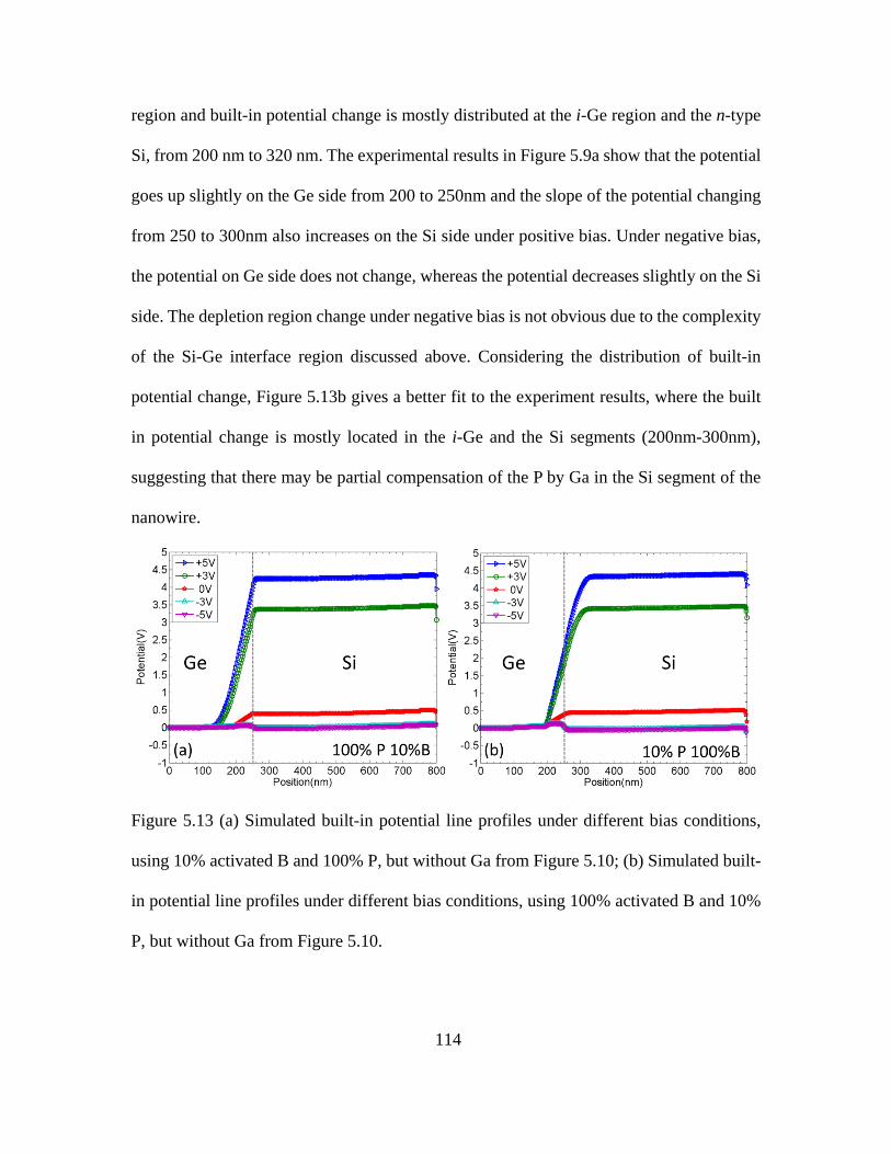
The results of APT measurement for a Ge-Si NW are shown in Figure 5.10. Within
the Ge segment, the B distribution decreases from a doping density of ~1019cm-3 at ~50 nm,
to background levels at ~200 nm, followed by i-Ge growth for ~50 nm which results from
the continued Ge NW growth in the absence of the B source during the lag time preceding
the catalyst alloying step. The heterointerface between Ge and Si occurs at a position of
~250nm, with a width of ~10 nm consistent with the same heterointerface width measured
previously by x-ray dispersive spectroscopy for very similar NWs [6]. Within the Si
106
segment, the P concentration increases monotonically from a dopant density of ~4×10¹⁸
cm-3 at the heterointerface, to 2×1020 cm-3 at the catalyst location. In addition to P,
unintentional incorporation of Ga is also observed in the Si segment. A spike in Ga
composition to ~6×1019 cm-3 is found at the heterointerface, followed by a relatively
constant profile of ~2×1019 cm-3 throughout the Si segment. A detailed discussion of the
reasons for the measured dopant profiles is outside the scope of this work, and will be the
subject of a separate paper.
Figure 5.10 B, P and Ga dopant profiles, and Si, Ge compositions of a typical Si-Ge
heterojunction NW measured using APT.
The controlled incorporation of dopants within the NW was intended to modulate the
carrier type and concentration to achieve desired transport characteristics. However, the
incorporation of unintentional impurities will complicate transport, especially when it has
the potential to compensate intentional carriers, such as in the current case for p-type Ga
107
and n-type P within the Si segment. From the profiles measured by APT, a constant Ga
doping density of 1-2×1019 cm-3 is observed in Si. If all dopants (B, P and Ga) are
considered to be electrically active, then all of the Ga in Si would act as a p-type dopant
and compensate the n-type P dopant, and the higher concentration dopant would determine
the effective type of dopant.
Figure 5.11 (a) Simulated built-in potential line profiles using different fractions of active
Ga, fully activated B and P from Figure 5.10, where legend shows the amount of active Ga;
(b) Simulated built-in potential line profiles using different fractions of active B and P, but
without Ga from Figure 5.10, where legend shows the amount of active B and P.
In order to estimate the active dopant distributions, SilvacoTM TCAD simulations
were performed for comparison with the APT and EH experiments. An abrupt Si-Ge
interface was assumed, and the dopant profiles (B, P and Ga) from APT shown in Figure
5.10 were used for the device simulation. This result suggests that this structure should
consist of n-type Si, to p-type Si, and then to i-Ge and finally p-type Ge. The simulated
potential profile assuming 100% dopant activation is shown by the blue line of Figure 5.11a.
108
The built-in potential of the n-type Si would be ~0.5V (at ~600nm), while the potential of
the p-type Si would be ~-0.4V (at ~400nm), relative to Ge (at ~0nm). Thus, this dopant
profile would result in a potential drop of ~0.9V in Si from the n-type segment to the p-
type segment and another 0.4V potential step across the SiGe interface with the Ge side
being higher. The slow potential decrease in Si from 600nm to ~800nm is caused by the P
dopant concentration decrease.
The unintentional Ga dopant in the Si part of the NW might incorporate interstitially,
or it could form Ga-vacancy defects or other small defect clusters and not be fully activated.
Thus, simulations with partially activated Ga are also shown in Figure 5.11a, where the
legend shows the fraction of activated Ga. With lower active Ga concentrations, the p-type
segment length in Si is reduced, while the potential offset between n-type Si and p-type Si
decreases slightly (less than 0.1V from 100% to 30%). When the active Ga is reduced to
concentrations lower than that of P (~20% of Ga dopant), the p-type Si segment disappears
and only one potential drop of ~0.5V is visible within Ge at ~250nm, effectively forming
an nip-like Si-Ge heterojunction. The experimental EH result from Figure 5.7b indicated
that the built-in potential had 0.4V offset across the Si-Ge interface and the potential for
the Ge side was always lower than for Si. Moreover, if there is a p-type Si segment, either
the Si-Ge heterointerface or the np junction in the Si segment would always be in reverse
bias and the current should be small until the junction breaks down. This situation is not
consistent with the I-V curve measurements, as shown in Figure 5.9b. These comparisons
suggest that the Ga is less than 20% activated. According to the literature [23], the solubility
of Ga in Si is lower than 1×1019 cm-3. Also, Ga dopants in Si have only been reported to be
active up to ~1018 cm-3 with only partial activation at higher concentrations due to the
109
relatively high activation energy [24-26]. Therefore, we conclude that only a small fraction
of the Ga atoms present are activated at most, and since the active Ga concentration must
be lower than that of the active P, its influence can be included in the simulations below
by the active P level.
In order to determine the activation of the P and B dopants, the built-in potentials
across the Si-Ge heterojunction were simulated using varying amounts of active P and B,
as shown in Figure 5.11b. These simulations show that the built-in potential offset between
Si and Ge is ~0.48V (at ~400nm relative to Ge at 0nm), with the Ge side lower, if both P
and B are fully activated (100% P and 100% B). If the active B is 100% and P is only 10%,
then the potential offset is reduced to 0.44V and if the active B is only 10% and P is 100%,
then the potential offset is 0.39V. Further reductions of the active P and B concentrations
by an order of magnitude did not affect the built-in potential offset by very much. Moreover,
most of the depletion and built-in potential change across the Si-Ge heterojunction
remained in the region from 200 nm to 250 nm so that the length of the depletion region
stayed at about the same size as the i-Ge segment (~50 nm). Since most of the built-in
potential increase from Ge to Si is in the i-Ge region, from 200 nm to 250 nm, a phase
increase in the Ge segment right before the Si-Ge interface would be expected at ~400nm
in Figure 5.7b. However, this signal was not observed in the experiment, possibly because
of the complexity of the SiGe interface and differences in MIP discussed above. The built-
in potential offset measured from the holography experiment was ~0.4±0.2 V, which
closely fitted the cases simulated for 10% B in Ge and 100% P in Si, and for 100% B in Ge
and 10% P in Si. However, the potential profile from the holography experiments was noisy
because of the NW surface irregularities and cannot readily distinguish the ~0.2 V
110
difference. Therefore, the amount of active P and B dopants cannot be accurately
determined under these experimental conditions, and it can only be concluded that either
100% active P and 10% B, or 10% P and 100% B give the closest fit between experiment
and simulations. A further comparison with simulation under biasing conditions is most
likely needed to determine the active dopant concentrations.
In Figure 5.7b, the total change of potential in the Si segment from 500nm to 650nm
is ~0.7 V, whereas the change of Si NW width, measured from the width profile in Figure
5.7a and 5.6d, is only 3%, which would only cause about 0.3 V difference. Moreover, the
potential in the Si segment extending from 450nm to 800nm in Figure 5.11b increases by
0.1 V because the dopant level increases close to the catalyst. Au has been reported to form
a Schottky contact with Si [13]. However, because the P dopant concentration near the
catalyst is so high, the built-in potential change due to the Schottky contact is limited to a
very small area adjacent to the catalyst and should not influence measurements across the
Si-Ge heterojunction, as shown at ~800nm in Figure 5.11b. Thus, the increase of potential
from 550nm to 650nm in Figure 5.7b can be partially explained by the combined effect of
diameter increase and P dopant concentration increase. The extra potential offset could be
due to diffraction near the catalyst.
111
Figure 5.12 Simulated band structure using 100% activated B and 10% P, but without Ga
from Figure 5.10.
To better understand the carrier transport properties of the NW, Figure 5.12 shows
the simulated band structure alignment using dopant profiles of 100% B and 10% P, as
measured from APT. The Fermi level is in the valence band on the Ge side due to the high
level of p-type dopant, while it is under but close to the conduction band on the Si side.
When the dopant level towards the catalyst increases to 1019 cm-3, the Fermi level on the
Si side gets closer to the conduction band. For a typical tunneling transistor, the Fermi level
on Si side should be in the conduction band and it should be in the valence band on the Ge
side across the Si-Ge interface. However, because the dopant level in Si near the SiGe
interface is not high enough, the Fermi level near the SiGe interface is still in the forbidden
band and electrons cannot easily tunnel through the interface. When the positive bias on Si
is increased, the band structure on the Si side is lower and electrons can then tunnel from
the Ge valence band to the Si conduction band. When negative bias is applied to Si, the
112
band structure on the Si side is higher so that electrons can move easily from the Si
conduction band to the Ge conduction band.
In order to interpret the in situ EH biasing experiments, further simulations were done
for a similar device structure, connecting the Si end to tungsten, forming a Schottky contact,
and connecting Ge to an ohmic contact. Bias from -5V to +5V was then applied on the Si
side, with the Ge side kept grounded. The simulated built-in potential profiles under bias
are shown in Figures 5.13a and 5.13b, where Figure 5.13a uses active dopants of 100% P
and 10% B, as measured from the APT results, and Figure 5.13b uses active dopants of 10%
P and 100% B. In both cases, the simulated built-in potential offset increases as the applied
positive bias increases, whereas it only decreases slightly under different negative bias. The
built-in potential of the Ge intrinsic region increases to a smaller amount as positive bias
is applied, whereas it only decreases slightly as negative bias is applied, which would cause
the change of dip observed in Figure 5.9a. The slope in potential, moving from Ge (200
nm) to Si (250 nm), also increases under positive bias, whereas the slope of the potential
decreases slightly under negative bias. Moreover, the depletion region and built-in potential
change under negative bias is mostly distributed in the i-Ge region, from 200nm to 250nm.
However, the distribution of depletion region and built-in potential change between the two
cases is different under positive bias. In Figure 5.13a, because of the high dopant
concentration of P in Si and relatively low concentration of B in Ge, most of the depletion
region and built-in potential change is in part of the p-type Ge region and the i-Ge region,
from 120 nm to 250 nm. There is only a very small built-in potential change region located
at the n-type Si segment, from 250 to 270nm. On the other hand, in Figure 5.13b, there is
a relative low concentration of P in Si and high concentration of B in Ge. The depletion
113
region and built-in potential change is mostly distributed at the i-Ge region and the n-type
Si, from 200 nm to 320 nm. The experimental results in Figure 5.9a show that the potential
goes up slightly on the Ge side from 200 to 250nm and the slope of the potential changing
from 250 to 300nm also increases on the Si side under positive bias. Under negative bias,
the potential on Ge side does not change, whereas the potential decreases slightly on the Si
side. The depletion region change under negative bias is not obvious due to the complexity
of the Si-Ge interface region discussed above. Considering the distribution of built-in
potential change, Figure 5.13b gives a better fit to the experiment results, where the built
in potential change is mostly located in the i-Ge and the Si segments (200nm-300nm),
suggesting that there may be partial compensation of the P by Ga in the Si segment of the
nanowire.
Figure 5.13 (a) Simulated built-in potential line profiles under different bias conditions,
using 10% activated B and 100% P, but without Ga from Figure 5.10; (b) Simulated built-
in potential line profiles under different bias conditions, using 100% activated B and 10%
P, but without Ga from Figure 5.10.
114
With positive bias applied, the Schottky contact is in forward bias and has low
resistance, while the Si-Ge heterojunction is in reverse bias and has high resistance. Thus,
most of the positive voltage would be distributed across the Si-Ge heterojunction. The
built-in potential offset across the heterojunction will increase as the bias increases. When
the bias exceeds a certain value, the Si conduction band will become low enough. Thus,
electrons from the Ge valence band can tunnel through the Si-Ge interface into the Si
conduction band, giving a rectifying effect in the IV curve, as shown in Figure 5.9b. With
negative bias, the Schottky contact is in reverse bias and has high resistance, while the Si-
Ge heterojunction is in forward bias. The resistance of the heterojunction is low compared
to the Schottky and ohmic contacts, and most of the negative voltage is distributed on the
contacts. Therefore, the built-in potential offset across the heterojunction will be close to
the one without bias and will not change much under different negative bias. Due to the
high dopant level in Si near the catalyst, electrons can tunnel through the Schottky contact
and thus there is still a rectifying effect due to the Si-Ge heterojunction, which is visible in
the IV curve in Figure 5.9b. Therefore, the change of dip and nearby Ge segment, as well
as the Si segment in Figure 5.9a, can be explained and the simulation results match well
with the in situ holography biasing experiment.
5.4 Conclusions
Doped Si-Ge heterojunction NWs have been grown using the VLS method, and APT
measurements were made to extract the B, P and Ga dopant concentrations as well as the
Si, Ge composition profiles. The electrostatic potential profile measured by electron
holography showed that the total potential offset across the Si-Ge heterojunction had the
115
value of 1.8±0.2V, with the Si side lower, whereas the built-in potential offset had the value
of 0.4±0.2V, with the Ge side lower because of the difference in MIP between Ge and Si.
Comparisons with simulations indicated that the Ga present in the Si region was, at most,
only partially activated and that its effect could be ignored. The P and B active dopants
could not be determined accurately due to noise from the irregular NW surface and
insensitivity in the depletion region length because of the i-Ge region. In situ biasing
experiments combined with electron holography were also performed. With positive bias
on Si, most of the voltage was distributed across the Si-Ge heterojunction and its built-in
potential increased to the same amount as the applied bias, whereas most of the voltage
was distributed on the contacts with negative bias on Si and the built-in potential across
the heterojunction was not changed much. Comparisons between biasing EH results and
simulations indicated that the B dopant in Ge is mostly activated but not the P dopant in Si,
possibly due to partial compensation by Ga in the Si region. The I−V characteristic curve
was measured and could also be explained using simulations. Overall, these results
demonstrated that off-axis electron holography, APT and TCAD simulations provide a
powerful combination for understanding the electrically active dopant distributions in
doped NW device heterostructures.
116
References
[1] Z. Gan, D. Perea, J. Yoo, Y. He, R. Colby, B. Barker, M. Gu, S. Mao, C. Wang, S. Tom Picraux, D. Smith, and M. McCartney, Unpublished (2015).
[2] M. S. Gudiksen, L. J. Lauhon, J. Wang, D. C. Smith, and C. M. Lieber, Nature 415 617 (2002).
[3] S. M. Sze, Physics of semiconductor devices, 2nd ed. Wiley, New York, (1981).
[4] V. Schmidt, H. Riel, S. Senz, S. Karg, W. Riess, and U. Gosele, Small 2 85 (2006).
[5] J. Goldberger, A. I. Hochbaum, R. Fan, and P. Yang, Nano letters 6 973 (2006).
[6] D. E. Perea, N. Li, R. M. Dickerson, A. Misra, and S. T. Picraux, Nano letters 11 3117 (2011).
[7] C. Y. Wen, M. C. Reuter, J. Bruley, J. Tersoff, S. Kodambaka, E. A. Stach, and F. M. Ross, Science 326 1247 (2009).
[8] L. Chen, W. Y. Fung, and W. Lu, Nano letters 13 5521 (2013).
[9] D. E. Perea, E. Wijaya, J. L. Lensch-Falk, E. R. Hemesath, and L. J. Lauhon, Journal of Solid State Chemistry 181 1642 (2008).
[10] D. E. Perea, E. R. Hemesath, E. J. Schwalbach, J. L. Lensch-Falk, P. W. Voorhees, and L. J. Lauhon, Nature nanotechnology 4 315 (2009).
[11] M. R. McCartney and D. J. Smith, Annual Review of Materials Research 37 729 (2007).
[12] M. R. McCartney, N. Agarwal, S. Chung, D. A. Cullen, M.-G. Han, K. He, L. Li, H. Wang, L. Zhou, and D. J. Smith, Ultramicroscopy 110 375 (2010).
[13] Z. Gan, D. E. Perea, J. Yoo, S. Tom Picraux, D. J. Smith, and M. R. McCartney, Applied Physics Letters 103 153108 (2013).
[14] L. Li, Z. Gan, M. R. McCartney, H. Liang, H. Yu, W. J. Yin, Y. Yan, Y. Gao, J. Wang, and D. J. Smith, Adv Mater 26 1052 (2014).
[15] M. I. den Hertog, H. Schmid, D. Cooper, J. L. Rouviere, M. T. Bjork, H. Riel, P. Rivallin, S. Karg, and W. Riess, Nano letters 9 3837 (2009).
[16] N. Li, T. Y. Tan, and U. Gösele, Applied Physics A 90 591 (2008).
[17] S. A. Dayeh, J. Wang, N. Li, J. Y. Huang, A. V. Gin, and S. T. Picraux, Nano letters 11 4200 (2011).
117
[18] S. A. Dayeh, N. H. Mack, J. Y. Huang, and S. T. Picraux, Applied Physics Letters 99 023102 (2011).
[19] J. E. Allen, E. R. Hemesath, D. E. Perea, J. L. Lensch-Falk, Z. Y. Li, F. Yin, M. H. Gass, P. Wang, A. L. Bleloch, R. E. Palmer, and L. J. Lauhon, Nature nanotechnology 3 168 (2008).
[20] M. J. Hytch, E. Snoeck, and R. Kilaas, Ultramicroscopy 74 131 (1998).
[21] J. Li, M. R. McCartney, R. E. Dunin-Borkowski, and D. J. Smith, Acta Crystallographica Section A 55 652 (1999).
[22] J. Li, M. R. McCartney, and D. J. Smith, Ultramicroscopy 94 149 (2003).
[23] F. A. Trumbore, Bell System Technical Journal 39 205 (1960).
[24] T. Hoshikawa, X. Huang, K. Hoshikawa, and S. Uda, Japanese Journal of Applied Physics 47 8691 (2008).
[25] K. B. Wolfstirn, Journal of Physics and Chemistry of Solids 16 279 (1960).
[26] N. Sclar, Electron Devices, IEEE Transactions on 24 709 (1977).
118
CHAPTER 6
CHARACTERIZATION OF TRAPPED CHARGES IN Ge/LixGe CORE/SHELL
STRUCTURE DURING LITHIATION USING OFF-AXIS ELECTRON
HOLOGRAPHY
This chapter describes the lithiation of Ge nanowires (NWs) and the measurement of
trapped charges in Ge/LixGe core/shell NWs using off-axis electron holography. The Ge
NWs were grown using the vapor-liquid-solid (VLS) method, and were provided by
Chongmin Wang and Meng Gu from Pacific Northwest National Laboratory. My
contribution to this work has included characterization of the NW lithiation process,
measurement of electrostatic profiles across the core/shell structures, and simulations for
estimation of the trapped charge.
6.1 Introduction
Lithium ion batteries (LIBs) have important applications as energy-storage systems
for portable electronics, electric vehicles, and sources of renewable energy such as wind
and solar [1,2]. Graphite is currently used as the anode material in commercial LIBs.
However, graphite has a limited theoretical capacity of 372 mAhg-1 and it cannot meet the
growing demands for high energy density and long life-time [3,4]. Novel materials such as
other group IV materials (Si, Ge and Sn), with higher theoretical capacities, are being
considered as possible alternatives [3]. Si has received most attention because of its greatest
theoretical capacity of 3579 mAhg-1 and 8334AhL-1 for Li15Si4 at room temperature, as
well as its abundance [5,6]. Relative to Si, Ge has lower theoretical capacities of 1384
119
mAhg-1 and 7366 AhL-1 for Li15Ge4 at room temperature, and it is more expensive [3,7].
However, Ge has higher intrinsic electronic conductivity because of its smaller band gap
(0.6eV) compared to Si (1.1eV) [8]. Moreover, the Li ion diffusivity in Ge is about two
times larger, compared to Si [9,10]. Thus, Ge has high charging/discharging rates in LIBs,
compared to Si, which is also an important consideration for LIB applications. Despite
these advantages, a major drawback of using Si or Ge is the huge volume change upon full
lithiation/delithiation (281% for Si and 246% for Ge), which may lead to degradation of
electrodes and the solid electrolyte interface (SEI), causing irreversible loss of LIB capacity
[11-15]. Nanostructures have been developed to accommodate the strain during lithiation
and to increase rate capability by shortening the Li ion diffusion length [16-18].
In situ transmission electron microscopy (TEM) has been used to characterize the
microstructure and phase transition behavior during lithiation/delithiation for several
materials, including Si, Ge and Sn, by using open cell structures with liquid or solid
Figure 6.5 Model for trapped charges in Ge/LixGe core/shell structure: (a) Schematic
diagram of the model; (b) Experimental data (black) and best fitted results (red).
Using the fitted charge density, the built-in potential distribution across the core/shell
structure can be plotted, as shown in Figure 6.6a, using pseudo-color to show the change
of potential. A potential profile is also extracted along the y=0 axis and shown in Figure
6.6b. This profile indicates that there is ~-2V potential difference between the shell and the
surface of the core, which fits with the bias experiment conditions. Extra electrons are
127
accumulated at the Ge core and thus reduced the measured total potential. The apparent
lower value of the mean inner potential described earlier can therefore be explained.
Figure 6.6 Simulation of potential distribution in Ge/LixGe core/shell NW: (a) Potential
distribution in NW cross section, shown in pseudo-color with scale bar on the right in units
of V; (b) Potential profile along Y=0 in (a).
The amount of Li (x) in the LixGe shell can also be estimated by using the volume
ratio and measured mean inner potential. The proposed equation is described below:
𝑚𝑚∙𝑉𝑉𝐿𝐿𝑖𝑖+𝑉𝑉𝐺𝐺𝑟𝑟𝑉𝑉𝐺𝐺𝑟𝑟
∙ � 𝑉𝑉𝑜𝑜𝑜𝑜𝐺𝐺𝑟𝑟𝑉𝑉𝑜𝑜𝑜𝑜𝐿𝐿𝑖𝑖𝑚𝑚𝐺𝐺𝑟𝑟
� = 𝑉𝑉𝐿𝐿𝑖𝑖𝑚𝑚𝐺𝐺𝑟𝑟𝑉𝑉𝐺𝐺𝑟𝑟
(6.1)
where VGe and VLixGe are the mean inner potentials for crystal Ge and LixGe, respectively,
VolGe and VolLixGe are the volumes for Ge and LixGe, respectively, and VLi is the mean
inner potential changed when one Li atom is added to Ge and the total volume is unchanged.
This equation also assumes that the MIP for Ge does not change during phase change.
The measured radius for core and the whole NW are shown in table 6.2, where case
A is before lithiation, case B, C and D are at the time corresponding to Figure 6.4a, 6.4d
and 6.4g, respectively. The case D at Figure 6.4g is used for calibration, where x is 128
approximated to be 3.75 for the fully lithiated phase and the volume ratio 𝑉𝑉𝑜𝑜𝑜𝑜𝐺𝐺𝑟𝑟𝑉𝑉𝑜𝑜𝑜𝑜𝐿𝐿𝑖𝑖𝑚𝑚𝐺𝐺𝑟𝑟
was
calculated to be 0.13. The value for VLi is then calculated to be 6.27V, using 14.3V MIP
for crystal Ge [26] and Equation 6.1. Since the core disappeared, there should be no trapped
charge in the NW structure, which might influence the result.
Table 6.2 Measured radius for NW core and whole NW.
Case Core (nm) Whole NW (nm) A - 66 B 45 88 C - 110 D - 129
After the calibration, the amount of Li x in LixGe can be calculated, again using
Equation 6.1. For case B at Figure 6.4a, the x in the NW shell is calculated to be 2.4 for
the measured MIP of 7.6V, where the effect of trapped charge was ignored, while x is
calculated to be 2.9 for the measured MIP of 8.4V, where effect of trapped charge was
included by using the best fitted model discussed above. These results indicate that the
intermediate lithiated state for NW shell is LixGe, where x is significantly lower than 3.75.
As the lithiation process continued, more Li might be diffused into the LixGe shell structure
and thus x was increased until it reached 3.75 and the NW was fully lithiated. The case C
cannot be calculated to confirm this result because the core is faceted and its cross section
area cannot be calculated. Further experiments and other methods might be necessary for
further investigation.
129
6.4 Conclusions
A Ge NW was lithiated in situ by applying 2V bias between its two ends, and TEM,
STEM and EELS were used to characterize the changes in the Ge/LixGe core/shell structure.
Electron holograms were taken during the lithiation process to determine the charge
distribution inside the NW. The mean inner potential for LixGe decreased during the
process, due to an increase of the Li content in the shell. Lower potential at the Ge core
was also discovered, and attributed to accumulation of trapped charge. A model was
proposed to explain the lower measured Ge potential, and the amount of trapped charge in
the Ge core was calculated to be 3×10¹⁸ electrons/cm3. The amount of Li during lithiation
was calculated using MIP and volume ratio. It suggests that the Li amount in LixGe during
lithiation might be lower than the fully lithiated phase and increased during the lithiation
process.
130
References
[1] M. Armand and J. M. Tarascon, Nature 451 652 (2008).
[2] A. S. Arico, P. Bruce, B. Scrosati, J.-M. Tarascon, and W. van Schalkwijk, Nature materials 4 366 (2005).
[3] D. Larcher, S. Beattie, M. Morcrette, K. Edstrom, J.-C. Jumas, and J.-M. Tarascon, Journal of Materials Chemistry 17 3759 (2007).
[4] Y.-M. Chiang, Science 330 1485 (2010).
[5] M. N. Obrovac and L. Christensen, Electrochemical and Solid-State Letters 7 A93 (2004).
[6] M. N. Obrovac and L. J. Krause, Journal of The Electrochemical Society 154 A103 (2007).
[7] L. Baggetto and P. H. L. Notten, Journal of The Electrochemical Society 156 A169 (2009).
[8] S. M. Sze, Physics of semiconductor devices, 2nd ed. Wiley, New York, (1981).
[9] C. Fuller and J. Severiens, Physical Review 96 21 (1954).
[10] J. Graetz, C. C. Ahn, R. Yazami, and B. Fultz, Journal of The Electrochemical Society 151 A698 (2004).
[11] X. H. Liu, Y. Liu, A. Kushima, S. Zhang, T. Zhu, J. Li, and J. Y. Huang, Advanced Energy Materials 2 722 (2012).
[12] L. Y. Beaulieu, K. W. Eberman, R. L. Turner, L. J. Krause, and J. R. Dahn, Electrochemical and Solid-State Letters 4 A137 (2001).
[13] C. K. Chan, H. Peng, G. Liu, K. McIlwrath, X. F. Zhang, R. A. Huggins, and Y. Cui, Nat Nano 3 31 (2008).
[14] X. H. Liu, H. Zheng, L. Zhong, S. Huang, K. Karki, L. Q. Zhang, Y. Liu, A. Kushima, W. T. Liang, J. W. Wang, J. H. Cho, E. Epstein, S. A. Dayeh, S. T. Picraux, T. Zhu, J. Li, J. P. Sullivan, J. Cumings, C. Wang, S. X. Mao, Z. Z. Ye, S. Zhang, and J. Y. Huang, Nano letters 11 3312 (2011).
[15] B. Key, R. Bhattacharyya, M. Morcrette, V. Seznéc, J.-M. Tarascon, and C. P. Grey, J Am Chem Soc 131 9239 (2009).
[16] P. G. Bruce, B. Scrosati, and J.-M. Tarascon, Angewandte Chemie International Edition 47 2930 (2008).
131
[17] L. Ji, Z. Lin, M. Alcoutlabi, and X. Zhang, Energy & Environmental Science 4 2682 (2011).
[18] H. Wu and Y. Cui, Nano Today 7 414 (2012).
[19] X. H. Liu, J. W. Wang, S. Huang, F. Fan, X. Huang, Y. Liu, S. Krylyuk, J. Yoo, S. A. Dayeh, A. V. Davydov, S. X. Mao, S. T. Picraux, S. Zhang, J. Li, T. Zhu, and J. Y. Huang, Nature nanotechnology 7 749 (2012).
[20] X. H. Liu, L. Q. Zhang, L. Zhong, Y. Liu, H. Zheng, J. W. Wang, J. H. Cho, S. A. Dayeh, S. T. Picraux, J. P. Sullivan, S. X. Mao, Z. Z. Ye, and J. Y. Huang, Nano letters 11 2251 (2011).
[21] Y. Liu, X. H. Liu, B. M. Nguyen, J. Yoo, J. P. Sullivan, S. T. Picraux, J. Y. Huang, and S. A. Dayeh, Nano letters 13 4876 (2013).
[22] X. H. Liu and J. Y. Huang, Energy & Environmental Science 4 3844 (2011).
[23] X. H. Liu, S. Huang, S. T. Picraux, J. Li, T. Zhu, and J. Y. Huang, Nano letters 11 3991 (2011).
[24] Y. Liu, S. Zhang, and T. Zhu, ChemElectroChem 1 706 (2014).
[25] M. Gu, H. Yang, D. E. Perea, J. G. Zhang, S. Zhang, and C. M. Wang, Nano letters 14 4622 (2014).
[26] J. Li, M. R. McCartney, R. E. Dunin-Borkowski, and D. J. Smith, Acta Crystallographica Section A 55 652 (1999).
132
CHAPTER 7
SUMMARY AND FUTURE WORK
7.1 Summary
The research of this dissertation has involved quantitative analysis of electrostatic
potential profiles and charge distributions in semiconductor nanostructures using off-axis
electron holography.
ZnO nanowires (NWs) and thin films have been investigated. The mean inner
potential (MIP) and inelastic mean free path (IMFP) of ZnO has been measured using ZnO
NWs. The MIP at 200keV was measured to be 15.3V±0.2V and the IMFP was measured
to be 55±3nm. The measured MIP agreed closely with the value reported in the literature.
The MIP and IMFP values were then used to measure the thickness of a ZnO nano-sheet
and gave consistent results for thicknesses in the range of 14nm-18nm.
ZnTe thin films have also been studied. The MIP was measured using intrinsic ZnTe
thin films and convergent beam electron diffraction (CBED). The MIP at 200keV was
measured to be 13.7±0.6V and the IMFP was measured to be 46±2nm. The MIP
measurement matched the value obtained by calculations. The measured MIP and IMFP
were then used to study a ZnTe thin film expected to have a p-n junction. However, no
change in signal due to built-in potential was observed across a junction. Possible reasons
might be: (a) the Al dopants were not activated; or (b) the junction was outside the field of
view of the holography experiment. Dynamical effects were systematically studied using
Bloch wave simulations. Thinner samples, avoiding low-index zone axes and careful
sample tilting will all help to minimize these effects.
133
Si NWs with axial p-n junctions and Schottky junction were investigated [1]. The
Schottky junctions were formed at the end of the NW due to the presence of Au catalyst
particles. The electrostatic potential profile measured by electron holography showed that
the built-in potentials across the p-n junction and the Schottky junction, had values of
1.0±0.3V and 0.5±0.3V, respectively. Simulations indicated that the dopant concentrations
were ~1019cm-3 for donors and ~1017 cm-3 for acceptors. The positively charged Au particle
at the end of the grounded NW had to be considered in order to account for the lower work
function in the simulation. The effects of a possible transition region forming an n+-n--p
junction, and possible surface charge, were also systematically studied using simulations.
Doped Si-Ge heterojunction NWs were investigated using off-axis electron
holography, while atom probe tomography (APT) measurements were made to extract the
B, P and Ga dopant concentrations as well as the Si, Ge composition profiles [2]. The
electrostatic potential profile measured by holography showed that the total potential offset
across the Si-Ge heterojunction had the value of 1.8±0.2V, with the Si side lower, whereas
the built-in potential offset had the value of 0.4±0.2V, with the Ge side lower because of
the difference in MIP between Ge and Si. Comparisons with simulations indicated that the
Ga dopant present in the Si was, at most, only partially activated and that its effect could
be ignored. The P and B active dopants could not be determined accurately due to noise
from the irregular NW surface and insensitivity in the depletion region length because of
the i-Ge region. In situ biasing experiments combined with electron holography were also
performed. With positive bias on Si, most voltage was distributed across the Si-Ge
heterojunction and its built-in potential increased to the same amount as the applied bias,
whereas most of the voltage was distributed on the contacts with negative bias on Si and
134
the built-in potential across the heterojunction was not much changed. Comparisons
between EH biasing results and simulations indicated that the B dopant in Ge was mostly
activated but not the P dopant in Si, possibly due to partial compensation by Ga in the Si
region. The I−V characteristic curve was measured and could also be explained using
simulations.
Ge/LixGe core/shell structures were studied during lithiation using S/TEM, EELS and
holography. The Ge NW was lithiated in situ by applying 2V bias between the two ends.
Electron holograms were taken during the lithiation process to determine the charge
distribution inside the NW. The MIP for LixGe decreased during the process, due to an
increase of the Li content in the shell. Lower potential at the Ge core was also discovered,
and attributed to accumulation of trapped charge. A model was proposed to explain the
lower measured Ge potential, and the amount of trapped electrons in the Ge core was
calculated to be 3×10¹⁸ electrons/cm3. The amount of Li during lithiation was calculated
using MIP values and the volume ratio. The results suggest that the amount of Li in LixGe
during lithiation might be lower than the fully lithiated phase but increased during the
lithiation process.
Overall, this dissertation research has reiterated that off-axis electron holography is
an effective technique for quantitative characterization of nanostructure thickness and
electrostatic potential profiles with nanoscale resolution. Combining electron holography
and simulations provides information about electrically active dopant and trapped charge
distributions in semiconductor nanostructures, which are important for understanding
electrical mechanisms and for developing future semiconductor devices. Moreover,
electron holography coupled with in situ biasing can be used to characterize devices under
135
working conditions and to extract information which is not shown under unbiased
conditions.
7.2 Remarks on Possible Future Work
This dissertation research has clearly demonstrated that electron holography is an
effective technique for quantitative characterization of built-in potential, and active dopants,
as well as trapped charges, with nanoscale resolution. However, electron holography only
gives two-dimensional projected-phase information about the sample. Uniform
composition and built-in potential distributions in the sample along the electron beam
direction were assumed in this dissertation research for calculations of active dopant
concentration. For semiconductor devices, the built-in potential may vary along the beam
direction due to surface effects or inhomogeneous dopant distributions. Therefore, it is
important to obtain three-dimensional phase information and hence the built-in potential
distribution in order to make accurate measurements of dopant amounts.
This problem can be solved by taking holograms at different tilt angles and using
tomographic reconstruction [3]. 3-D holography characterization of Si thin films with p-n
junctions has been reported [4], and it was found that the surface active dopant
concentrations were lower, whereas the central ones were very close, compared to bulk
material. NWs have a large surface-to-volume ratio and the surface may play an important
role in overall dopant distributions. A preliminary tomography experiment has been
performed on Si-Ge axial heterojunction NWs using HAADF STEM tilt image series, as
shown in Figure 7.1. The tilt series were taken using FEI Titan G2 80-300 operated at
300kV. The sample was tilted from -70˚ to 70˚ and the HAADF images were taken every
136
2˚. Figure 7.1a shows a typical image that was taken at 0˚ tilt angle. The intensity from
HAADF image is directly related to the atomic number and thickness of the sample, and
therefore it satisfies the tomography reconstruction requirements. The data was
reconstructed by INSPECT3DTM using the simultaneous iterative reconstruction technique
(SIRT) algorithm with 20 iterations. The result is shown in Figure 7.1b, using pseudo-color
to show the change of intensity, and the cross section of the NW is shown in Figure 7.1c.
From the HAADF image tomography reconstruction, the composition distribution is
almost uniform in cross section and the NW grown along <111> direction has a hexagonal
cross section. However, the HAADF image is not sensitive to the dopant concentrations
nor the built-in potential. Further tomographic holography experiments are necessary so
that the three-dimensional phase as well as the built-in potential distribution can be
extracted. The active dopants in all three dimensions could thus be determined by
comparison with simulations.
137
Figure 7.1 Tomography of Si-Ge NWs: (a) HAADF image at 0˚ tilt; (b) Tomography
reconstruction result shown in pseudo color; (c) Cross section of NW.
138
References
[1] Z. Gan, D. E. Perea, J. Yoo, S. Tom Picraux, D. J. Smith, and M. R. McCartney, Applied Physics Letters 103 153108 (2013).
[2] Z. Gan, D. Perea, J. Yoo, Y. He, R. Colby, B. Barker, M. Gu, S. Mao, C. Wang, S. Tom Picraux, D. J. Smith, and M. R. McCartney, submitted (2015).
[3] J. Frank, Electron tomography : three-dimensional imaging with the transmission electron microscope. Plenum Press, New York, (1992).
[4] A. C. Twitchett-Harrison, T. J. Yates, R. E. Dunin-Borkowski, and P. A. Midgley, Ultramicroscopy 108 1401 (2008).
139
LIST OF REFERENCES
A. C. Twitchett-Harrison, T. J. Yates, R. E. Dunin-Borkowski, and P. A. Midgley, Ultramicroscopy 108 1401 (2008).
A. C. Jones, M. L. Hitchman, and Knovel (Firm), Chemical vapour deposition precursors, processes and applications. Royal Society of Chemistry, Cambridge, UK, (2009).
A. Lubk, D. Wolf, and H. Lichte, Ultramicroscopy 110 438 (2010).
A. S. Arico, P. Bruce, B. Scrosati, J.-M. Tarascon, and W. Van Schalkwijk, Nature materials 4 366 (2005).
A. Sekar, S. H. Kim, A. Umar, and Y. B. Hahn, Journal of Crystal Growth 277 471 (2005).
A. T. Heitsch, D. D. Fanfair, H.-Y. Tuan, and B. A. Korgel, J Am Chem Soc 130 5436 (2008).
A. Tonomura, Reviews of Modern Physics 59 639 (1987).
A. Umar and Y. B. Hahn, Nanotechnology 17 2174 (2006).
A. Umar, S. H. Kim, Y. S. Lee, K. S. Nahm, and Y. B. Hahn, Journal of Crystal Growth 282 131 (2005).
A. Umar, S. Lee, Y. S. Lee, K. S. Nahm, and Y. B. Hahn, Journal of Crystal Growth 277 479 (2005).
A. V. Crewe and J. Wall, Journal of Molecular Biology 48 375 (1970).
B. G. Yacobi, Semiconductor materials : an introduction to basic principles. Kluwer Academic/Plenum Publishers, New York, (2003).
B. Key, R. Bhattacharyya, M. Morcrette, V. Seznéc, J.-M. Tarascon, and C. P. Grey, J Am Chem Soc 131 9239 (2009).
B. P. Zhang, N. T. Binh, K. Wakatsuki, Y. Segawa, Y. Yamada, N. Usami, M. Kawasaki, and H. Koinuma, Applied Physics Letters 84 4098 (2004).
B. Pal and M. Sharon, Mater Chem Phys 76 82 (2002).
C. C. Ahn, Transmission electron energy loss spectrometry in materials science and the EELS atlas, 2nd ed. Wiley, Weinheim, Germany, (2004).
C. Fuller and J. Severiens, Physical Review 96 21 (1954).
140
C. J. Lee, T. J. Lee, S. C. Lyu, Y. Zhang, H. Ruh, and H. J. Lee, Applied Physics Letters 81 3648 (2002).
C. K. Chan, H. Peng, G. Liu, K. McIlwrath, X. F. Zhang, R. A. Huggins, and Y. Cui, Nat Nano 3 31 (2008).
C. Y. Wen, M. C. Reuter, J. Bruley, J. Tersoff, S. Kodambaka, E. A. Stach, and F. M. Ross, Science 326 1247 (2009).
D. A. Neamen, Semiconductor physics and devices : basic principles, 2nd ed. Irwin, Chicago, (1997).
D. A. Neamen, Semiconductor physics and devices : basic principles, 3rd ed. McGraw-Hill Higher Education, London, (2003).
D. B. Williams and C. B. Carter, Transmission electron microscopy : a textbook for materials science, 2nd ed. Springer, New York, (2009).
D. C. Ghiglia and M. D. Pritt, Two-dimensional phase unwrapping : theory, algorithms, and software. Wiley, New York, (1998).
D. Cooper, C. Ailliot, J.-P. Barnes, J.-M. Hartmann, P. Salles, G. Benassayag, and R. E. Dunin-Borkowski, Ultramicroscopy 110 383 (2010).
D. E. Perea, E. R. Hemesath, E. J. Schwalbach, J. L. Lensch-Falk, P. W. Voorhees, and L. J. Lauhon, Nature nanotechnology 4 315 (2009).
D. E. Perea, E. Wijaya, J. L. Lensch-Falk, E. R. Hemesath, and L. J. Lauhon, Journal of Solid State Chemistry 181 1642 (2008).
D. E. Perea, N. Li, R. M. Dickerson, A. Misra, and S. T. Picraux, Nano letters 11 3117 (2011).
D. Gabor, Proceedings of the Royal Society of London. Series A. Mathematical and Physical Sciences 197 454 (1949).
D. Larcher, S. Beattie, M. Morcrette, K. Edstrom, J.-C. Jumas, and J.-M. Tarascon, Journal of Materials Chemistry 17 3759 (2007).
E. Koren, N. Berkovitch, O. Azriel, A. Boag, Y. Rosenwaks, E. R. Hemesath, and L. J. Lauhon, Applied Physics Letters 99 223511 (2011).
E. Müller, P. Kruse, D. Gerthsen, M. Schowalter, A. Rosenauer, D. Lamoen, R. Kling, and A. Waag, Applied Physics Letters 86 154108 (2005).
E. N. Leith and J. Upatnieks, J. Opt. Soc. Am. 52 1123 (1962).
F. A. Trumbore, Bell System Technical Journal 39 205 (1960). 141
F. M. Ross and W. M. Stobbs, Philosophical Magazine A 63 37 (1991).
F. Qian, Y. Li, S. Gradecak, D. L. Wang, C. J. Barrelet, and C. M. Lieber, Nano letters 4 1975 (2004).
G. E. Moore, Proceedings of the IEEE 86 82 (1998).
G. Mandel, Physical Review 134 A1073 (1964).
G. Möllenstedt and H. Wahl, Naturwissenschaften 55 340 (1968).
G. Radi, Acta Crystallographica Section A 26 41 (1970).
G. Sberveglieri, S. Groppelli, P. Nelli, A. Tintinelli, and G. Giunta, Sensors and Actuators B: Chemical 25 588 (1995).
G.-C. Yi, Semiconductor Nanostructures for Optoelectronic Devices Processing, Characterization and Applications, Springer, Heidelberg, (2012).
H. Bethe, Ann. Phys. 87 55 (1928).
H. Kai, C. Jeong-Hyun, J. Yeonwoong, S. T. Picraux, and C. John, Nanotechnology 24 115703 (2013).
H. Lichte, P. Formanek, A. Lenk, M. Linck, C. Matzeck, M. Lehmann, and P. Simon, Annual Review of Materials Research 37 539 (2007).
H. Wu and Y. Cui, Nano Today 7 414 (2012).
I. Kimukin, M. S. Islam, and R. S. Williams, Nanotechnology 17 S240 (2006).
I. W. Tao, M. Jurkovic, and W. I. Wang, Applied Physics Letters 64 1848 (1994).
International Technology Roadmap for Semiconductors 2013, available online at http://www.itrs.net.
J. C. H. Spence and J. M. Zuo, Electron microdiffraction. Plenum Press, New York, (1992).
J. E. Allen, E. R. Hemesath, D. E. Perea, J. L. Lensch-Falk, Z. Y. Li, F. Yin, M. H. Gass, P. Wang, A. L. Bleloch, R. E. Palmer, and L. J. Lauhon, Nature nanotechnology 3 168 (2008).
J. Frank, Electron tomography : three-dimensional imaging with the transmission electron microscope. Plenum Press, New York, (1992).
J. Goldberger, A. I. Hochbaum, R. Fan, and P. Yang, Nano letters 6 973 (2006).
142
J. Graetz, C. C. Ahn, R. Yazami, and B. Fultz, Journal of The Electrochemical Society 151 A698 (2004).
J. Ibers, Acta Crystallographica 11 178 (1958).
J. J. Lee, Y. B. Kim, and Y. S. Yoon, Applied Surface Science 244 365 (2005).
J. Li, M. R. McCartney, and D. J. Smith, Ultramicroscopy 94 149 (2003).
J. Li, M. R. McCartney, R. E. Dunin-Borkowski, and D. J. Smith, Acta Crystallographica Section A 55 652 (1999).
J. M. Cowley, Ultramicroscopy 41 335 (1992).
J. Q. Hu, Y. Bando, J. H. Zhan, Y. B. Li, and T. Sekiguchi, Applied Physics Letters 83 4414 (2003).
J. Spence, Acta Crystallographica Section A 49 231 (1993).
J. W. Dailey, J. Taraci, T. Clement, D. J. Smith, J. Drucker, and S. T. Picraux, J Appl Phys 96 7556 (2004).
J. Xiang, W. Lu, Y. Hu, Y. Wu, H. Yan, and C. M. Lieber, Nature 441 489 (2006).
J. Y. Tsao, Materials fundamentals of molecular beam epitaxy. Academic Press, Boston, (1993).
K. B. Wolfstirn, Journal of Physics and Chemistry of Solids 16 279 (1960).
K. Sato, M. Hanafusa, A. Noda, A. Arakawa, M. Uchida, T. Asahi, and O. Oda, Journal of Crystal Growth 214–215 1080 (2000).
L. Baggetto and P. H. L. Notten, Journal of The Electrochemical Society 156 A169 (2009).
L. Chen, W. Y. Fung, and W. Lu, Nano letters 13 5521 (2013).
L. J. Lauhon, M. S. Gudiksen, C. L. Wang, and C. M. Lieber, Nature 420 57 (2002).
L. Ji, Z. Lin, M. Alcoutlabi, and X. Zhang, Energy & Environmental Science 4 2682 (2011).
L. Li, D. J. Smith, E. Dailey, P. Madras, J. Drucker, and M. R. McCartney, Nano letters 11 493 (2011).
143
L. Li, Z. Gan, M. R. McCartney, H. Liang, H. Yu, W. J. Yin, Y. Yan, Y. Gao, J. Wang, and D. J. Smith, Adv Mater 26 1052 (2014).
L. Reimer, Transmission electron microscopy : physics of image formation and microanalysis, 4th ed. Springer, New York, (1997).
L. Y. Beaulieu, K. W. Eberman, R. L. Turner, L. J. Krause, and J. R. Dahn, Electrochemical and Solid-State Letters 4 A137 (2001).
MultiPrepTM operating manual of Allied High Tech Products, Inc.
M. A. Herman and H. Sitter, Molecular beam epitaxy : fundamentals and current status, 2nd, rev. and updated ed. Springer, New York, (1996).
M. Armand and J. M. Tarascon, Nature 451 652 (2008).
M. Faraday, Experimental researches in electricity. R. and J.E. Taylor, London, (1839).
M. Gajdardziska-Josifovska and A. H. Carim, Chapter 12, Introduction to electron holography, Kluwer Academic/Plenum Publishers, New York, (1999).
M. Gajdardziska-Josifovska, M. R. McCartney, W. J. de Ruijter, D. J. Smith, J. K. Weiss, and J. M. Zuo, Ultramicroscopy 50 285 (1993).
M. Gu, H. Yang, D. E. Perea, J. G. Zhang, S. Zhang, and C. M. Wang, Nano letters 14 4622 (2014).
M. H. Huang, S. Mao, H. Feick, H. Yan, Y. Wu, H. Kind, E. Weber, R. Russo, and P. Yang, Science 292 1897 (2001).
M. I. den Hertog, H. Schmid, D. Cooper, J. L. Rouviere, M. T. Bjork, H. Riel, P. Rivallin, S. Karg, and W. Riess, Nano letters 9 3837 (2009).
M. J. Hytch, E. Snoeck, and R. Kilaas, Ultramicroscopy 74 131 (1998).
M. Lehmann and H. Lichte, Microscopy and Microanalysis 8 447 (2004).
M. Lehmann, Ultramicroscopy 100 9 (2004).
M. N. Obrovac and L. Christensen, Electrochemical and Solid-State Letters 7 A93 (2004).
M. N. Obrovac and L. J. Krause, Journal of The Electrochemical Society 154 A103 (2007).
M. R. McCartney and D. J. Smith, Annual Review of Materials Research 37 729 (2007).
M. R. McCartney and M. Gajdardziska-Josifovska, Ultramicroscopy 53 283 (1994). 144
M. R. McCartney, N. Agarwal, S. Chung, D. A. Cullen, M.-G. Han, K. He, L. Li, H. Wang, L. Zhou, and D. J. Smith, Ultramicroscopy 110 375 (2010).
M. S. Gudiksen, L. J. Lauhon, J. Wang, D. C. Smith, and C. M. Lieber, Nature 415 617 (2002).
M. Schowalter, D. Lamoen, A. Rosenauer, P. Kruse, and D. Gerthsen, Applied Physics Letters 85 4938 (2004).
M. Y. Kim, J. M. Zuo, and J. C. H. Spence, physica status solidi (a) 166 445 (1998).
M.-S. Kim and Y.-M. Sung, Chem Mater 25 4156 (2013).
N. Li, T. Y. Tan, and U. Gösele, Applied Physics A 90 591 (2008).
N. Ohashi, K. Kataoka, T. Ohgaki, T. Miyagi, H. Haneda, and K. Morinaga, Applied Physics Letters 83 4857 (2003).
N. Sclar, Electron Devices, IEEE Transactions on 24 709 (1977).
O. Hayden, A. B. Greytak, and D. C. Bell, Advanced Materials 17 701 (2005).
O. Hiroshi, I. Gheyas Syed, N. Hitoshi, N. Mitsuhiro, and Y. Akira, Japanese Journal of Applied Physics 33 L980 (1994).
P. A. Doyle and P. S. Turner, Acta Crystallographica Section A 24 390 (1968).
P. A. Tipler, Modern physics. Worth Publishers, New York, (1978).
P. Becker and P. Coppens, Acta Crystallographica Section A 46 254 (1990).
P. G. Bruce, B. Scrosati, and J.-M. Tarascon, Angewandte Chemie International Edition 47 2930 (2008).
P. Hartel, H. Rose, and C. Dinges, Ultramicroscopy 63 93 (1996).
P. M. Voyles, D. A. Muller, J. L. Grazul, P. H. Citrin, and H. J. Gossmann, Nature 416 826 (2002).
R. Agarwal, Small 4 1872 (2008).
R. F. Egerton, Electron energy-loss spectroscopy in the electron microscope, 2nd ed. Plenum Press, New York, (1996).
R. S. Wagner and W. C. Ellis, Applied Physics Letters 4 89 (1964).
S. A. Dayeh, J. Wang, N. Li, J. Y. Huang, A. V. Gin, and S. T. Picraux, Nano letters 11 4200 (2011). 145
S. A. Dayeh, N. H. Mack, J. Y. Huang, and S. T. Picraux, Applied Physics Letters 99 023102 (2011).
S. Baosheng, Y. Akira, and K. Makoto, Japanese Journal of Applied Physics 37 L206 (1998).
S. Dimitrijev, Understanding semiconductor devices. Oxford University Press, New York, (2000).
S. Ingole, P. Manandhar, S. B. Chikkannanavar, E. A. Akhadov, and S. T. Picraux, Electron Devices, IEEE Transactions on 55 2931 (2008).
S. J. Pennycook, P. D. Nellist, Scanning Transmission Electron Microscopy Imaging and Analysis. Springer, New York, NY, (2011).
S. M. Sze, Physics of semiconductor devices, 2nd ed. Wiley, New York, (1981).
S. M. Sze, Physics of semiconductor devices. Wiley-Interscience, New York, (1969).
S. M. Sze, Semiconductor devices, physics and technology, 2nd ed. Wiley, New York, (2002).
S. Miyake, Proc. Phys. Math. Soc. Japan 22 666 (1940).
T. E. Clark, P. Nimmatoori, K.-K. Lew, L. Pan, J. M. Redwing, and E. C. Dickey, Nano letters 8 1246 (2008).
T. Hoshikawa, X. Huang, K. Hoshikawa, and S. Uda, Japanese Journal of Applied Physics 47 8691 (2008).
T. Tanaka, K. Hayashida, K. Saito, M. Nishio, Q. Guo, and H. Ogawa, physica status solidi (b) 243 959 (2006).
T. Tanaka, N. Murata, K. Saito, M. Nishio, Q. Guo, and H. Ogawa, physica status solidi (b) 244 1685 (2007).
T. Tanaka, Q. Guo, M. Nishio, and H. Ogawa, Journal of Physics: Conference Series 61 1162 (2007).
T. Teiji, M. Toyosaka, and T. Kiyoshi, Japanese Journal of Applied Physics 11 1024 (1972).
U. K. Mishra, J. Singh, Semiconductor device physics and design. Springer, Dordrecht, The Netherlands, (2008).
U. Özgür, Y. I. Alivov, C. Liu, A. Teke, M. A. Reshchikov, S. Doğan, V. Avrutin, S. J. Cho, and H. Morkoç, Journal of Applied Physics 98 041301 (2005).
146
V. Schmidt, H. Riel, S. Senz, S. Karg, W. Riess, and U. Gosele, Small 2 85 (2006).
V. Schmidt, J. V. Wittemann, S. Senz, and U. Gösele, Advanced Materials 21 2681 (2009).
W. D. Callister, T. L. Larsen, C. F. Varotto, and D. A. Stevenson, Journal of Physics and Chemistry of Solids 33 1433 (1972).
W. Lu, J. Xiang, B. P. Timko, Y. Wu, and C. M. Lieber, Proc. Nat. Acad. Sci. 102 10046 (2005).
W. Lu, P. Xie, and C. M. Lieber, IEEE Transactions on Electron Devices 55 2859 (2008).
X. H. Liu and J. Y. Huang, Energy & Environmental Science 4 3844 (2011).
X. H. Liu, H. Zheng, L. Zhong, S. Huang, K. Karki, L. Q. Zhang, Y. Liu, A. Kushima, W. T. Liang, J. W. Wang, J. H. Cho, E. Epstein, S. A. Dayeh, S. T. Picraux, T. Zhu, J. Li, J. P. Sullivan, J. Cumings, C. Wang, S. X. Mao, Z. Z. Ye, S. Zhang, and J. Y. Huang, Nano letters 11 3312 (2011).
X. H. Liu, J. W. Wang, S. Huang, F. Fan, X. Huang, Y. Liu, S. Krylyuk, J. Yoo, S. A. Dayeh, A. V. Davydov, S. X. Mao, S. T. Picraux, S. Zhang, J. Li, T. Zhu, and J. Y. Huang, Nature nanotechnology 7 749 (2012).
X. H. Liu, L. Q. Zhang, L. Zhong, Y. Liu, H. Zheng, J. W. Wang, J. H. Cho, S. A. Dayeh, S. T. Picraux, J. P. Sullivan, S. X. Mao, Z. Z. Ye, and J. Y. Huang, Nano letters 11 2251 (2011).
X. H. Liu, S. Huang, S. T. Picraux, J. Li, T. Zhu, and J. Y. Huang, Nano letters 11 3991 (2011).
X. H. Liu, Y. Liu, A. Kushima, S. Zhang, T. Zhu, J. Li, and J. Y. Huang, Advanced Energy Materials 2 722 (2012).
X. Y. Kong, Y. Ding, R. Yang, and Z. L. Wang, Science 303 1348 (2004).
Y. C. Kong, D. P. Yu, B. Zhang, W. Fang, and S. Q. Feng, Applied Physics Letters 78 407 (2001).
Y. Cui, Q. Wei, H. Park, and C. M. Lieber, Science 293 1289 (2001).
Y. Hu, H. O. Churchill, D. J. Reilly, J. Xiang, C. M. Lieber, and C. M. Marcus, Nature nanotechnology 2 622 (2007).
Y. Li, G. W. Meng, L. D. Zhang, and F. Phillipp, Applied Physics Letters 76 2011 (2000).
147
Y. Liu, S. Zhang, and T. Zhu, ChemElectroChem 1 706 (2014).
Y. Liu, X. H. Liu, B. M. Nguyen, J. Yoo, J. P. Sullivan, S. T. Picraux, J. Y. Huang, and S. A. Dayeh, Nano letters 13 4876 (2013).
Y. Wu, Y. Cui, L. Huynh, C. J. Barrelet, D. C. Bell, and C. M. Lieber, Nano letters 4 433 (2004).
Y.-C. Chou, C.-Y. Wen, M. C. Reuter, D. Su, E. A. Stach, and F. M. Ross, ACS Nano 6 6407 (2012).
Y.-M. Chiang, Science 330 1485 (2010).
Z. Gan, D. E. Perea, J. Yoo, S. Tom Picraux, D. J. Smith, and M. R. McCartney, Applied Physics Letters 103 153108 (2013).
Z. Gan, D. Perea, J. Yoo, Y. He, R. Colby, B. Barker, M. Gu, S. Mao, C. Wang, S. Tom Picraux, D. Smith, and M. McCartney, Unpublished (2015).
Z. L. Wang, Journal of Physics: Condensed Matter 16 R829 (2004).
Z. W. Pan, Z. R. Dai, and Z. L. Wang, Science 291 1947 (2001).