Characterization of multi-walled carbon nanotube–polymer nanocomposites by scanning spreading resistance microscopy This article has been downloaded from IOPscience. Please scroll down to see the full text article. 2012 Nanotechnology 23 405704 (http://iopscience.iop.org/0957-4484/23/40/405704) Download details: IP Address: 129.187.254.47 The article was downloaded on 21/03/2013 at 14:51 Please note that terms and conditions apply. View the table of contents for this issue, or go to the journal homepage for more Home Search Collections Journals About Contact us My IOPscience
Transcript
Characterization of multi-walled carbon nanotube–polymer nanocomposites by scanning
spreading resistance microscopy
This article has been downloaded from IOPscience. Please scroll down to see the full text article.
Received 4 June 2012, in final form 15 August 2012Published 20 September 2012Online at stacks.iop.org/Nano/23/405704
AbstractNanocomposites of aligned multi-walled carbon nanotubes (CNTs) embedded in a polymermatrix yield a unique combination of thermal and electrical properties and mechanicalstrength. These properties are intimately related to the composite nanostructure and to thegrowth and processing conditions. The alignment of the tubes, the filling fraction and thecontact junction between the nanotubes are key parameters controlling the compositeelectrical conductivity. For this purpose, a full description of the composite nanostructure isrequired. Among the non-destructive scanning probe techniques, scanning spreadingresistance microscopy is found to be a powerful technique in identifying the carbon nanotubeswith true nanometer resolution, thus competing with SEM and TEM imaging. Additionally,the technique provides valuable information about the electrical conduction mechanism withinthe composite structure. Indeed, by using a controlled contact force and an appropriate modelof conduction at the nanoscale, the tip–CNT contact resistance, the CNT intrinsic resistanceand the CNT–epoxy–CNT resistance junction are evaluated. This latter is found to be thefactor controlling the overall electrical conductivity of the composite.
(Some figures may appear in colour only in the online journal)
1. Introduction
There is a growing trend to incorporate nanostructuredmaterials, such as carbon nanotubes (CNTs), into polymericfilms to improve their overall performance [1–4]. Recentprogress in the manufacture of CNT–polymer nanocom-posites (CNT–PNCs), in particular those featuring alignednanotubes, promises a unique combination of optical,electrical, thermal and mechanical properties. The two majorapplications of nanocomposites with this set of characteristicsare (1) hybrid heterojunction solar cells [5, 6] which are basedon dispersed semiconducting CNTs and (2) nano-engineeredhybrid CNT based composites for the structural and aerospaceindustries [7–10]. Enhancement of the composite electricalproperties requires a high degree of CNT alignment, a highpacking density, and very small contact junctions betweennanotubes. The latter is the most critical since it leads to the
formation of tunneling junctions between the CNTs and thepolymer, leading to a significant decrease of the electricalconductivity by several orders of magnitude.
An in-depth description of the nanostructure correlatedwith an understanding of the transport phenomena isrequired to design and manufacture composites with thedesired properties. While it is critical to characterize thecomposite structure, only a few techniques are suitablefor this purpose. Structural studies commonly rely onscanning and transmission electron microscopy (SEM/TEM).Nevertheless, undesired structural changes can occur in thecharacterization process [11–13]. Alternatively, conductingprobe atomic force microscopy is used to characterize carbonnanotube and carbon nanofiber composites. Electrostaticforce microscopy (EFM) has been used for CNT networkmapping [14–16] and the dielectric response of CNT–polymercomposites [17]. Unfortunately, to date, the lateral resolution
reported in the literature is limited to 100 nm under ambientconditions [18–20]. Only under high vacuum can a lateralresolution of 10–20 nm be achieved by employing eitherfrequency modulation (FM) [21] or amplitude modulation(AM) [22, 23]. Kelvin probe force microscopy (KPFM) hasalso been used for structural and electrical characterizationof nanotubes in organic solar cells, but the technique ischaracterized by a similar lateral resolution to EFM due tothe long-range electrostatic force [24–26].
Current sensing atomic force microscopy (CS-AFM) andscanning spreading microscopy have been used to study thestructural ‘network and agglomeration’ of CNT and carbonnanofiber (CNF) based polymer composites [27–29]. To thebest of our knowledge, the CS-AFM and SSRM techniqueshave not been used to study the electrical transport behaviorof CNT–polymer composites. On the other hand, CS-AFMand SSRM have been used to probe the electrical propertiesof aligned CNFs [30] and CNTs [31, 32] encapsulated inSiO2 and dispersed multiwalled CNTs (MWCNTs) on goldfilm [33].
In this paper, we employ lateral force microscopy (LFM)and scanning spreading resistance microscopy (SSRM) toreveal the nanostructure and electrical characterization ofaligned multiwalled CNT–epoxy nanocomposites. The LFMis based on sensing the friction forces between the AFM tipand the sample, while the SSRM uses a similar CS-AFM setupbut with a specific amplifier allowing current sensing over 10orders of magnitude. This technique is extensively used tostudy semiconductor materials and devices [34]. The imagingcapabilities of the two techniques are compared to SEM andTEM imaging. Thanks to the high spatial resolution (∼4 nm),the SSRM technique yields an estimation of the CNT fillingfraction that is in agreement with what is obtained from SEMimages. Moreover the versatility of the technique (wide-rangecurrent sensing), in addition to providing the estimation ofthe tunneling resistance of CNT–epoxy junctions, allows usto investigate in-depth the electrical transport behavior withinCNT–polymer nanocomposites.
2. Material preparation
The composite material is made of a forest of verticallyaligned nanotubes embedded in an epoxy matrix. A schematicdescription of the process is given in figure 1. Firstly,the nanotubes are grown aligned on a quartz substrate bycatalytic chemical vapor deposition (CCVD) as describedin [35]. The resultant CNT forest (about 1.4 mm thick)is annealed at 2000 ◦C for 2 h in argon to produce highpurity MWCNTs. During this process, the iron impurities,observed in the CNT cores, are almost dissolved. In orderto form the composite, the CNT forest is impregnated byepoxy, making sure that the polymer infiltrates uniformlybetween the tubes. The epoxy used here is a mixture of47 wt% of Epon (Epon 812), 52.2 wt% of MNA (methyl-5-norbornene-2,3-dicarboxylic anhydride-C10H10O3) and 0.8wt% of DMP30 (2,4,6-Tris(dimethylaminomethyl)phenol-[(CH3)2NCH2]3C6H2OH). The resultant samples are cured at60 ◦C for four days, ground with SiC papers (400–4000) and
Figure 1. A schematic description of the manufacturing process ofCNT–polymer nanocomposites: (1) growth of the MWCNT forestusing CCVD with toluene as the carbon source and ferrocene as thecatalytic particles, (2) impregnation with epoxy resin in a vacuumchamber in order to improve the polymer infiltration between CNTs,(3) adjustment of the composite length by mechanical grinding from400 to 4000 SiC followed by fine diamond paste polishing.
finally polished using diamond paste of 1 and 0.25 µm. Thefinal composite thickness is 540 µm.
3. Results and discussion
3.1. Structural characterization of the CNT carpets
Figures 2(a) and (b) reveal the structure of the CNT forestwith low and high magnification SEM imaging (FEI 250Quanta FEG, under high vacuum and at 5 kV). On topof the forest, the CNTs have an entangled structure whichcorroborates the reported growth mechanism [35]. In contrast,the MWCNTs appear well aligned in the middle; onlythis region is used to form the nanocomposite. Howeverhigh magnification images reveal that the aligned CNTsare in contact with each other; also some short CNTs aregrown in the transverse direction creating T-junctions withaligned CNTs. These points of contact may form tunnelingjunctions between CNT and CNT or with an interlayingepoxy layer (after polymer encapsulation) decreasing furtherthe composite electrical conductivity. TEM imaging (FEITecnai G2) is also used to obtain the diameter distributionof the MWCNTs. For this purpose, a small piece of CNTforest is dispersed in an ethanol solution and then transferredto a TEM grid for observation and statistical investigation.Figures 3(a) and (b) show TEM images of the diameters of theMWCNTs before and after annealing. We note the existenceof iron nanowires encapsulated inside the cores of as-grownCNTs; after annealing almost all the particles are eliminated.These nanowires grow from catalyst particles [36, 37] duringthe CNT growth and are γ -Fe and/or FeC3. During heattreatment at 2000 ◦C, the nanowires migrate outside the tubesleaving the CNT-ends open. Figures 3(c) and (d) shows thestatistical distribution of the external diameters of the tubes.The annealing process does not involve strong modification ofthe CNT diameters. The obtained tube diameters are normallydistributed; the external diameters lie between 10 and 110 nmwith an average value of 48 nm, while the internal diametersvary from 3 to 10 nm with a mean value of 7 nm.
2
Nanotechnology 23 (2012) 405704 T Souier et al
Figure 2. (a) SEM images of the as-grown CNT forest on a quartz substrate, (b) high magnification SEM imaging of the central regions ofthe forest showing the CNT alignments. Point contacts between aligned CNTs and with short perpendicular CNTs are revealed.
Figure 3. (a), (b) TEM images of the diameters of the MWCNTs before and after annealing at 2000 ◦C, the scale bar is 200 nm. (c), (d) Thestatistical distribution of external diameter before and after the heating treatment. The annealing process appears to be of benefit in terms of(1) removing the iron nanowires, (2) decreasing the structural defects and enhancing the CNT crystallinity, while (3) the tube diameterremains stable.
3.2. Structural characterization of the composite
After the composite preparation, the as-polished sampleis characterized by means of SEM. Particular care ispaid in our analysis to the quality of the interface,i.e. CNT–external contact, as it is a main factor affectingelectrical conductivity measurements. It is worth mentioningthat the grinding/polishing was employed not only to adjust
the composite length but more importantly to (1) removethe forest’s top side that contains entangled CNTs structure,(2) remove the forest bottom side that contains the catalystparticles (base growth mechanism) and (3) protrude the CNTsfrom the polymer matrix.
Figures 4(a) and (b) show SEM images of the as-polishedcomposite surface in two cases where (1) the electron beamis perpendicular to the sample surface (figure 4(a)) and (2)
3
Nanotechnology 23 (2012) 405704 T Souier et al
Figure 4. SEM images of the as-polished composite surface (a) in top view showing CNT ends, (b) in inclined view showing the CNTsprotruding from the polymer matrix after mechanical polishing. The scale bar = 200 nm. The top view images allow estimation of theCNT packing density (∼15 vol%) while the inclined view gives an idea about the CNTs’ protruding length.
the sample is tilted by 42◦ (figure 4(b)). In the top view SEMimage, The CNT ends appear open and some of them are notfully circular; the missing parts are probably removed duringthe mechanical polishing procedure.
The diameters of individual CNTs observed by means ofSEM confirm the observation previously carried out by meansof TEM. However, the SEM images reveal the presence ofnano-objects with diameters greater than 150 nm. This canbe interpreted as agglomeration of some adjacent CNTs withthe polymer or formation of CNT bundles. In tilted views,the CNTs are protruding from the polymer matrix by aboutten nanometers which is probably due to the high mechanicalpolishing since the epoxy is very soft in comparison to theCNTs.
Since the electrical properties of the composite dependstrongly on the content and distribution of CNT fibers, astatistical analysis has been carried out on several SEMimages. The results show that the density of CNTs is 4.3 ×10¹³ CNT m−2 (±1.5 × 10¹³ CNT m−2) and their averagesurface fraction is about 15%.
In the following sections, SPM techniques are employedin order to complete the structural characterization of thecomposite. We aim to obtain information about the protrudinglength of the CNTs from the polymer matrix and also toestimate the packing density. Furthermore, the main questionthat we aim to address is whether or not the SPM techniquecan be used as an alternative and non-destructive method forprobing the properties of CNT filler composite. Moreover,we aim to address the question of whether the SPM allowsaccess to other information such as electrical properties andthe transport mechanism of aligned-CNT–PNCs.
a specific module for current measurements. The standardCS-AFM module [38] consists of a linear amplifier (withone gain, typically 1 G�) allowing current sensing from10 pA up to 10 nA. In order to study the wide rangeof conductivity in CNT–PNCs we used a transimpedancelogarithmic amplifier which allows current measurementsover 10 decades of magnitude, from 1 pA up to 1 mA [39, 40].This technique is called the SSRM technique especially whenhigh force is applied; the measured resistance is dominated bythe ‘spreading resistance’ which is proportional to the sampleelectrical resistivity [34, 39].
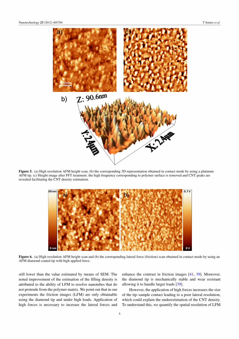
The height images reveal the existence of topographicpeaks that can be identified as individual CNTs (figures 5(a)and (b)). From the 2D representation of height image(figure 5(a)), the obtained CNT diameters agree with theestimation by SEM with an average value of 50 nm.The length of protruding CNTs is estimated from the 3Drepresentation (figure 5(b)) by using Igor software; it isshown that the CNTs protrude up to 80 nm and the averageprotruding length is 36 nm.
Our main concern is the estimation of the density andthe volume fraction of CNTs in the composite. Since theCNTs are aligned along the composite length, this fractionmay be approximated as the surface fraction. The first wayto obtain this value is to perform a fast Fourier transform(FFT) of the height images in order to subtract the polymerroughness and reveal the CNT peaks. Figure 5(c) showsthe resultant topography image after an FFT treatment offigure 5(a); the contrast in the new image is increased andthe CNTs are revealed. This method yields a CNT density of∼1013 CNT/m2–1.65×1013 CNT m−2 which is three or fourtimes lower than the density obtained by SEM imaging. Thisis most probably due to (1) the fact that some CNTs are notextending enough from the polymer matrix, and (2) the AFMtip not being sharp enough to distinguish between relativelyclose CNTs that form bundles or agglomerates.
In order to derive a correct reading of the CNT volumedensity, lateral force images are recorded by monitoringthe lateral movements of the cantilever. Note, for example,how figure 6(b) shows a better contrast in the friction scanswhen using a diamond tip. Here the average CNT densityis estimated as 2.5 × 10¹³ CNT/m2. This density is indeedhigher than the one obtained from the height images but
4
Nanotechnology 23 (2012) 405704 T Souier et al
Figure 5. (a) High resolution AFM height scan, (b) the corresponding 3D representation obtained in contact mode by using a platinumAFM tip. (c) Height image after FFT treatment: the high frequency corresponding to polymer surface is removed and CNT peaks arerevealed facilitating the CNT density estimation.
Figure 6. (a) High resolution AFM height scan and (b) the corresponding lateral force (friction) scan obtained in contact mode by using anAFM diamond coated tip with high applied force.
still lower than the value estimated by means of SEM. Thenoted improvement of the estimation of the filling density isattributed to the ability of LFM to resolve nanotubes that donot protrude from the polymer matrix. We point out that in ourexperiments the friction images (LFM) are only obtainableusing the diamond tip and under high loads. Application ofhigh forces is necessary to increase the lateral forces and
enhance the contrast in friction images [41, 39]. Moreover,the diamond tip is mechanically stable and wear resistantallowing it to handle larger loads [39].
However, the application of high forces increases the sizeof the tip–sample contact leading to a poor lateral resolution,which could explain the underestimation of the CNT density.To understand this, we quantify the spatial resolution of LFM
5
Nanotechnology 23 (2012) 405704 T Souier et al
Figure 7. (a) A schematic representation of the SSRM setup. (b) A schematic representation of the two terminal macroscopicmeasurements. (c) A 7 µm× 7 µm resistance image obtained with a low load (6 nN). (d) A high magnification image, 1.6 µm× 1.6 µm.The CNT backing densities estimated from SSRM scans match well those obtained from SEM imaging.
by measuring the tip–sample contact size through the Hertzformula [42]
a = (3RtipP/4E∗)1/3
1/E∗ = (1− υ2tip)/Etip + (1− υ2
s )/Es
where P is the contact force, Rtip = 100 nm is the tip radius,E∗ is the effective Young’s modulus, υtip = υs = 0.33 arethe Poison’s ratios of the tip and the sample, Es is the elasticmodulus of the CNT (1 TPa) and Etip is the Young’s modulusof the diamond tip (1.2 TPa).
For a given force of P ∼ 800 nN, a typical force usedfor LFM imaging, the mechanical contact size between thediamond tip and the CNT is approximately 2a ∼ 18 nm. Sincean MWCNT is composed of separated walls, only a tube withexternal diameter higher than 36 nm could be resolved. Takinginto account the diameter distribution of the annealed CNTsobtained by TEM, only 60% of the tubes can be resolved byLFM. This is exactly the ratio between the two CNT densitiesobtained by SEM and LFM.
A way to circumvent the above challenges relates tothe use of SSRM. With this technique both structural andelectrical properties (resistance) of the sample are acquiredsimultaneously in contact mode. In this mode, the images areobtained with a lower load that in turn improves the spatialresolution. Figure 7(a) shows a schematic representation ofthe SSRM setup used. The technique is a two terminalmeasurement, where one electrode is a conductive AFM tipand the second one is, in this case, a conductive sampleholder. Thus, the obtained spreading resistance images (R =V/I) correspond to the vertical resistance along the alignedCNTs. The SSRM imaging is carried out using the twoconductive tips. We present only the case of using a platinumtip where the most relevant results were obtained. Figures 7(c)and (d) show the typical resistance images obtained atdifferent magnifications with a low load (6 nN). The resistanceimages (figure 7(c)) reveal high resistance regions (black) thatcorrespond to the polymer matrix and high conducting ones(red–green–blue) corresponding to the CNTs. The averagediameter of the conductive spot is about 50 nm which isin good agreement with the TEM analysis. Furthermore,
C-AFM (resistance) scans give a CNT density of ≈4.8 ×10¹³ CNT/m2
± 0.5× 10¹³ CNT m−2. This agrees perfectlywith the value obtained from the SEM analysis. Indeed, if wetake a load of 6 nN and use the above equations applied tothe case of platinum tip (Rtip = 30 nm and Etip = 168 GPa),the corresponding size of the mechanical tip–CNT is 3.7 nm.With this value, all the nanotubes with an external diameterhigher than 10 nm are resolved in the images.
At even higher magnification, some features of thecomposite structure that are revealed by SEM can alsobe identified by SSRM. For instance, the open top CNTstructures are also observed in high resolution SSRM imageswhich are in concordance with the SEM results.
3.3. Electrical characterization of the composite
After a full structural characterization by means ofvarious techniques, the study can be directed towards thecharacterization of the electrical transport of the system,beginning at the macro-scale before the nanoscale. Themeasurement at macro-scale is based on two and four probeterminal electrical measurements (figure 7(b)). Crossed goldelectrodes ∼300 µm wide and 100 nm thick were evaporatedon both sides of the composite. The electrical conductancewas found to be of the order of 0.08 S in the vertical direction.Assuming that the electrical transport is mainly at the crossedarea of the two gold electrodes, the corresponding compositeelectrical conductivity can be estimated by using Ohm’s law,σcomp = CW2/L, where C is the measured conductance of∼0.08 S,W = 300 µm is the width of the gold electrodeand L = 540 µm is the length of the composite. This leadsto a composite electrical conductivity of 300 S m−1 whichis the highest resistivity in CNT–epoxy composites andamong the highest reported conductivities in CNT–polymercomposites [43–46].
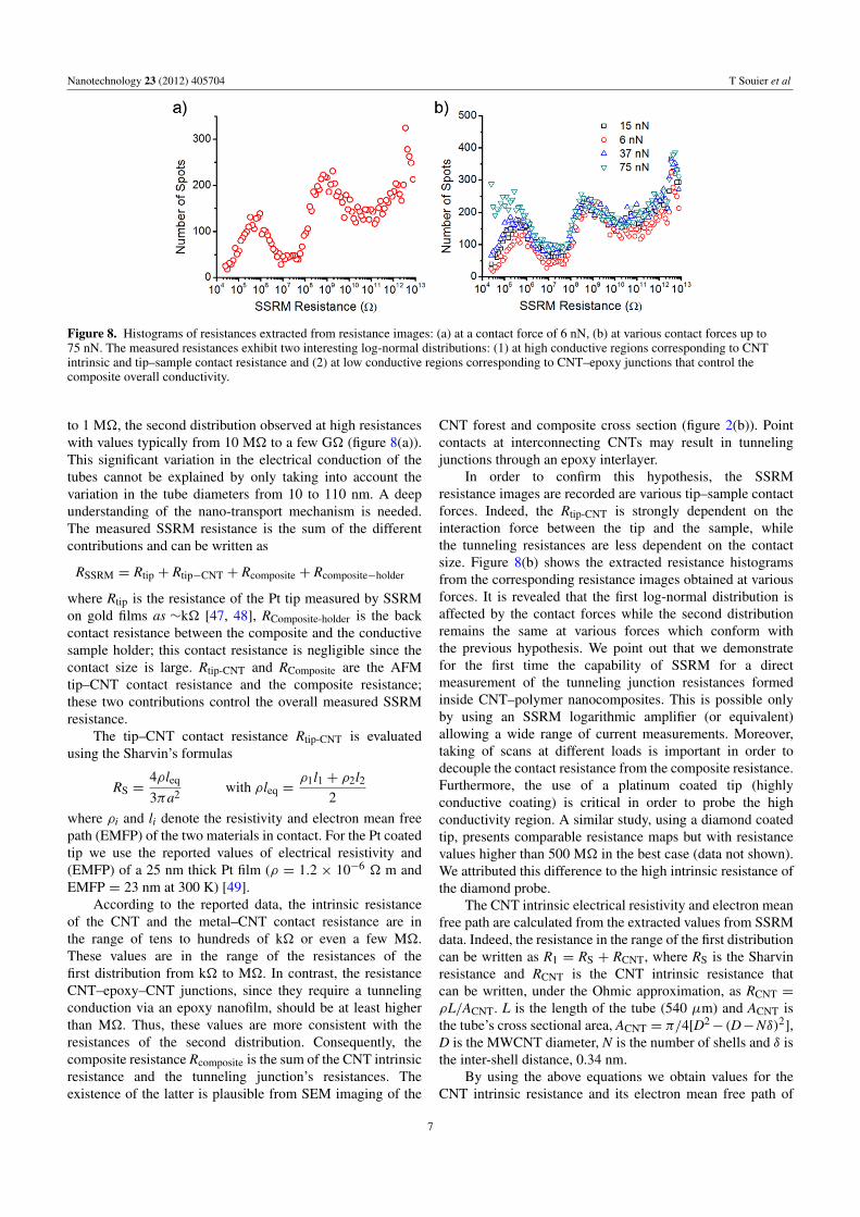
On the other hand, the electrical resistance of CNTsmeasured by SSRM at controlled contact force is foundto vary from 10 k� to 10 G�, thus more than 7 ordersof magnitude (figure 7(c)). Moreover, the histogram ofresistances extracted from figure 7(c) exhibits two log-normaldistributions: the first one at low resistances from a few k�
6
Nanotechnology 23 (2012) 405704 T Souier et al
Figure 8. Histograms of resistances extracted from resistance images: (a) at a contact force of 6 nN, (b) at various contact forces up to75 nN. The measured resistances exhibit two interesting log-normal distributions: (1) at high conductive regions corresponding to CNTintrinsic and tip–sample contact resistance and (2) at low conductive regions corresponding to CNT–epoxy junctions that control thecomposite overall conductivity.
to 1 M�, the second distribution observed at high resistanceswith values typically from 10 M� to a few G� (figure 8(a)).This significant variation in the electrical conduction of thetubes cannot be explained by only taking into account thevariation in the tube diameters from 10 to 110 nm. A deepunderstanding of the nano-transport mechanism is needed.The measured SSRM resistance is the sum of the differentcontributions and can be written as
where Rtip is the resistance of the Pt tip measured by SSRMon gold films as ∼k� [47, 48], RComposite-holder is the backcontact resistance between the composite and the conductivesample holder; this contact resistance is negligible since thecontact size is large. Rtip-CNT and RComposite are the AFMtip–CNT contact resistance and the composite resistance;these two contributions control the overall measured SSRMresistance.
The tip–CNT contact resistance Rtip-CNT is evaluatedusing the Sharvin’s formulas
RS =4ρleq
3πa2 with ρleq =ρ1l1 + ρ2l2
2
where ρi and li denote the resistivity and electron mean freepath (EMFP) of the two materials in contact. For the Pt coatedtip we use the reported values of electrical resistivity and(EMFP) of a 25 nm thick Pt film (ρ = 1.2 × 10⁻⁶ � m andEMFP = 23 nm at 300 K) [49].
According to the reported data, the intrinsic resistanceof the CNT and the metal–CNT contact resistance are inthe range of tens to hundreds of k� or even a few M�.These values are in the range of the resistances of thefirst distribution from k� to M�. In contrast, the resistanceCNT–epoxy–CNT junctions, since they require a tunnelingconduction via an epoxy nanofilm, should be at least higherthan M�. Thus, these values are more consistent with theresistances of the second distribution. Consequently, thecomposite resistance Rcomposite is the sum of the CNT intrinsicresistance and the tunneling junction’s resistances. Theexistence of the latter is plausible from SEM imaging of the
CNT forest and composite cross section (figure 2(b)). Pointcontacts at interconnecting CNTs may result in tunnelingjunctions through an epoxy interlayer.
In order to confirm this hypothesis, the SSRMresistance images are recorded are various tip–sample contactforces. Indeed, the Rtip-CNT is strongly dependent on theinteraction force between the tip and the sample, whilethe tunneling resistances are less dependent on the contactsize. Figure 8(b) shows the extracted resistance histogramsfrom the corresponding resistance images obtained at variousforces. It is revealed that the first log-normal distribution isaffected by the contact forces while the second distributionremains the same at various forces which conform withthe previous hypothesis. We point out that we demonstratefor the first time the capability of SSRM for a directmeasurement of the tunneling junction resistances formedinside CNT–polymer nanocomposites. This is possible onlyby using an SSRM logarithmic amplifier (or equivalent)allowing a wide range of current measurements. Moreover,taking of scans at different loads is important in order todecouple the contact resistance from the composite resistance.Furthermore, the use of a platinum coated tip (highlyconductive coating) is critical in order to probe the highconductivity region. A similar study, using a diamond coatedtip, presents comparable resistance maps but with resistancevalues higher than 500 M� in the best case (data not shown).We attributed this difference to the high intrinsic resistance ofthe diamond probe.
The CNT intrinsic electrical resistivity and electron meanfree path are calculated from the extracted values from SSRMdata. Indeed, the resistance in the range of the first distributioncan be written as R1 = RS + RCNT, where RS is the Sharvinresistance and RCNT is the CNT intrinsic resistance thatcan be written, under the Ohmic approximation, as RCNT =
ρL/ACNT. L is the length of the tube (540 µm) and ACNT isthe tube’s cross sectional area, ACNT = π/4[D2
− (D−Nδ)2],D is the MWCNT diameter, N is the number of shells and δ isthe inter-shell distance, 0.34 nm.
By using the above equations we obtain values for theCNT intrinsic resistance and its electron mean free path of
7
Nanotechnology 23 (2012) 405704 T Souier et al
ρ ∼ 10−6 �m and l ∼ 480 nm and these values are for all thecontact forces used. Also we deduce a CNT linear resistivityof 10 k� µm−1. These values are in the range of the reporteddata on high purity CNTs [50–52]. This result shows that thecomposite processing does not affect the electrical propertiesof individual MWCNTs.
Besides this, we can explain the variation of CNTresistances between a few k� and a few M� by taking intoaccount the tube diameter measured from TEM imaging.Indeed, by changing the tube diameter from 10 to 110 nmand using an MWCNT resistivity of ρ ∼ 10−6 � m, thecorresponding CNT resistance varies from a few M� to a fewk�.
The second distribution with resistance values of200 M�–2 G� corresponds to electrical conduction alongthe composite. The measured high resistance value of thecomposite is attributed to the tunneling junctions created atthe point contacts between the aligned CNTs as describedabove in the SEM analysis. Taking the resistance valueRcomposite in the range of 200 M�–2 G�, the compositeelectrical conductivity can be estimated locally using Ohm’slaw as ρcomposite = RL/A, where A is the cross sectionof the nanotube in contact with the AFM tip. For thecalculation, we take the cross section corresponding to theaverage CNT diameter of 48 nm (see the TEM analysis).The volume electrical resistivity of the composite is foundto vary from 100 to 900 S m−1 with an average valueof 350 S m−1. Despite the simplifications, the proposedmodel gives values of local conductivities that match wellthe composite resistivity measured by macroscopic probetechniques. A more detailed study based on the tunnelingmechanism through CNT–epoxy–CNT junctions is currentlyunderway in our group.
4. Conclusions
Structural characterization of aligned CNT–polymer compos-ite with a high packing density (15 vol%) is fully describedusing various techniques such as electron and scanningprobe microscopy. The AFM and LFM techniques yield anunderestimated value of the CNT filling density. The firstlimitation is due to the incapability of the AFM to resolveCNTs with short protruding length. The second limitationis due to the high forces required for LFM imaging thatlower the spatial resolution. However, thanks to the versatilityof the SSRM instrument and to the high spatial resolutionof ∼4 nm, the estimated filling density matches the SEManalysis perfectly, making SSRM an acceptable alternativeand non-destructive technique to characterize CNT basednanocomposites. In addition, SSRM is found to be a powerfultechnique to estimate the volume electrical conductivityof the composite in agreement with two and four probemacroscopic measurements. The information obtained fromthe investigation presented in our work has the potentialto help in understanding the conduction phenomena at thenanoscale, with an eye towards further improvement of thematerial processing of CNT–polymer nanocomposites.
References
[1] Chou T W, Gao L, Thostenson E T, Zhang Z andByun J H 2010 An assessment of the science andtechnology of carbon nanotube-based fibers and compositesCompos. Sci. Technol. 70 1–19
[2] Cebeci H, Guzman de Villoria R, Hart A J andWardle B L 2009 Multifunctional properties of high volumefraction aligned carbon nanotube polymer composites withcontrolled morphology Compos. Sci. Technol. 69 2649–56
[3] Breuer O and Sundararaj U 2004 Big returns from smallfibers: a review of polymer/carbon nanotube compositesPolym. Compos. 25 630–45
[4] Bauhofer W and Kovacs J Z 2009 A review and analysis ofelectrical percolation in carbon nanotube polymercomposites Compos. Sci. Technol. 69 1486–98
[5] Ren S, Bernardi M, Lunt R, Bulovic V, Grossman J C andGradecak S 2011 Toward efficient carbon nanotube/P3HTsolar cells: active layer morphology, electrical, and opticalproperties Nano Lett. 11 5316–21
[6] Gu H and Swager T M 2008 Fabrication of free-standing,conductive, and transparent carbon nanotube films Adv.Mater. 20 4433–7
[7] Megalini1 L, Saito D S, Garcia E J, Hart A J andWardle B L 2009 Impedance of aligned carbon nanotubearrays and polymeric nanocomposites J. Nano Syst.Technol. 1 1–16
[8] Prolongo S G, Campo M, Gude M R, Chaos-Moran R andUrena A 2009 Thermophysical characterisation of epoxyresin reinforced by amino-functionalized carbon nanofibersCompos. Sci. Technol. 69 349–57
[9] Prolongo S G, Gude M R, Sanchez J and Urena A 2009Nanoreinforced epoxy adhesives for aerospace industryJ. Adhes. 85 180–99
[10] Prolongo S G, Gude M R and Urena A 2009 Synthesis andcharacterisation of epoxy resins reinforced with carbonnanotubes and nanofibers J. Nanosci. Nanotechnol.9 6181–7
[11] Banhart F 1999 Irradiation effects in carbon nanostructuresRep. Prog. Phys. 62 1181
[12] Li J and Banhart F 2004 The engineering of hot carbonnanotubes with a focused electron beam Nano Lett.4 1143–6
[13] Yuzvinsky T D, Fennimore A M, Mickelson W,Esquivias C and Zettl A 2005 Precision cutting ofnanotubes with a low-energy electron beam Appl. Phys.Lett. 86 053109
[14] Jespersen T S and Nygard J 2007 Mapping of individualcarbon nanotubes in polymer/nanotube composites usingelectrostatic force microscopy Appl. Phys. Lett. 90 183108
[15] Kader M A, Choi D, Lee S K and Nah C 2005 Morphology ofconducting filler-reinforced nitrile rubber composites byelectrostatic force microscopy Polym. Test. 24 363–6
[16] Gu X, Knorr D B Jr, Wang G and Overney R M 2012 Layeredand interfacially blended polyelectrolyte multi-walledcarbon nanotube composites for enhanced ionicconductivity Thin Solid Films 520 1872–9
[17] Zhao M, Gu X, Lowther S E, Park C, Jean Y C andNguyen T 2010 Subsurface characterization of carbonnanotubes in polymer composites via quantitative electricforce microscopy Nanotechnology 21 225702
[18] Henning A K, Hochwitz T, Slinkman J, Never J, Hoffmann S,Kaszuba P and Daghlian C 1995 Two-dimensional surfacedopant profiling in silicon using scanning Kelvin probemicroscopy J. Appl. Phys. 77 1888
[19] Gaillard N, Gros-Jean M, Mariolle D, Bertin F andBsiesy A 2006 Method to assess the grain crystallographicorientation with a submicronic spatial resolution usingKelvin probe force microscope Appl. Phys. Lett. 89 154101
[20] Sinensky A K and Belcher A M 2007 Label-free andhigh-resolution protein/DNA nanoarray analysis usingKelvin probe force microscopy Nature Nanotechnol.2 653–9
[21] Zerweck U, Loppacher C, Otto T, Grafstrom S andEng L M 2007 Kelvin probe force microscopy of C60 onmetal substrates: towards molecular resolutionNanotechnology 18 084006
[22] Sommerhalter C, Glatzel T, Matthes T, Jager-Waldau A andLux-Steiner M C 2000 Kelvin probe force microscopy inultra high vacuum using amplitude modulation detection ofthe electrostatic Appl. Surf. Sci. 157 263–8
[23] Enevoldsen G H, Glatzel T, Christensen M C,Lauritsen J V and Besenbacher F 2008 Atomic scale kelvinprobe force microscopy studies of the surface potentialvariations on the TiO2(110) surface Phys. Rev. Lett.100 236104
[24] Liu L and Li G 2010 Electrical characterization ofsingle-walled carbon nanotubes in organic solar cells byKelvin probe force microscopy Appl. Phys. Lett. 96 083302
[25] Yu G, Gao J, Hummelen J C, Wudl F and Heeger A J 1995Polymer photovoltaic cells: enhanced efficiencies via anetwork of internal donor–acceptor heterojunctions Science270 1789–91
[26] Brunel D, Deresmes D and Melin T 2009 Determination of theelectrostatic lever arm of carbon nanotube field effecttransistors using Kelvin force microscopy Appl. Phys. Lett.94 223508
[27] Mdarhri A, Carmona F, Brosseau C and Delhaes P 2008Direct current electrical and microwave properties ofpolymer-multiwalled carbon nanotubes composites J. Appl.Phys. 103 054303
[28] Phang I Y, Liu T, Zhang W D, Schonherr H andVancso G J 2007 Probing buried carbon nanotubes withinpolymer–nanotube composite matrices by atomic forcemicroscopy Eur. Polym. J. 43 4136–42
[29] Trionfi A, Scrymgeour D A, Hsu J W P, Arlen M J, Tomllin D,Jacobs J D, Wang D H, Tan L S and Vaia R A 2008 Directimaging of current paths in multiwalled carbon nanofiberpolymer nanocomposites using conducting-tip atomic forcemicroscopy J. Appl. Phys. 104 083708
[30] Fourdrinier L, Poche H L, Chevalier N, Mariolle D andRouviere E 2008 Electrical properties measurements onindividual carbon nanofibers by scanning spreadingresistance microscopy J. Appl. Phys. 104 114305
[31] Li J, Ye Q, Cassell A, Ng H T, Stevens R, Han J andMeyyappan M 2003 Bottom-up approach for carbonnanotube interconnects Appl. Phys. Lett. 82 2491
[32] Li J, Stevens R, Delzeit L, Ng H T, Cassell A, Han J andMeyyappan M 2002 Electronic properties of multiwalledcarbon nanotubes in an embedded vertical array Appl. Phys.Lett. 81 910
[33] Dominiczak M, Otubo L, Alamarguy D, Houze F, Volz S,Noel S and Bai J 2011 Evaluation of the nanotube intrinsicresistance across the tip-carbon nanotube-metal substratejunction by atomic force microscopy Nanoscale Res. Lett.6 355
[34] Eyben P, Vandervorst W, Alvarez D, Xu M andFouchier M 2007 Probing semiconductor technology anddevices with scanning spreading resistance microscopyScanning Probe Microscopy 2nd edn, ed S Kalinin andA Gruverman (New York: Springer) pp 31–87
[35] Pinault M, Pichot V, Khodja H, Launois P, Reynaud C andMayne-L’Hermite M 2005 Evidence of sequential lift in
growth of aligned multiwalled carbon nanotube multilayersNano Lett. 5 2394–8
[36] Pinault M, Mayne-L’Hermite M, Reynaud C, Beyssac O,Rouzaud J N and Clinard C 2004 Carbon nanotubesproduced by aerosol pyrolysis: growth mechanisms andpost-annealing effects Diamond Relat. Mater. 13 1266–9
[37] Bouchet-Fabre B, Pinault M, Pichot V, Launois P,Mayne L’Hermite M, Parent Ph, Laffon K, Durand D andReynaud C 2005 NEXAFS and x-ray scattering study ofstructure changes after post-annealing treatments of alignedMWNTs Diamond Relat. Mater. 14 881–6
[38] Souier T, Martin F, Battalion C and Cousty J 2010 Localelectrical characteristics of passive films formed onstainless steel surfaces by current sensing atomic forcemicroscopy Appl. Surf. Sci. 256 2434–9
[39] Souier T, Li G, Santos S, Stefancich M and Chiesa M 2012Conductive scanning probe microscopy of nanostructuredBi2Te3 Nanoscale 4 600–6
[40] Souier T and Chiesa M 2012 Effect of surface conditions andstrain hardening on the passivity breakdown of 304stainless steel J. Mater. Res. 27 1580–8
[41] Bhushan B, Israelachvili J N and Landman U 1995Nanotribology: friction, wear and lubrication at the atomicscale Nature 374 607–16
[42] Johnson K L 1985 Contact Mechanics (Cambridge:Cambridge University Press)
[43] Kilbride B E, Coleman J N, Fraysse J, Fournet P, Cadek M,Drury A, Hutzler S, Roth S and Blau W J 2002Experimental observation of scaling laws for alternatingcurrent and direct current conductivity in polymer–carbonnanotube composite thin films J. Appl. Phys. 92 4024
[44] McNally T, Potschke P, Halley P, Murphy M, Martin D,Bell S E J, Brennan G P, Bein D, Lemoine P andQuinn J P 2005 Polyethylene multiwalled carbon nanotubecomposites Polymer 46 8222
[45] Ramasubramaniam R, Chen J and Liu H Y 2003Homogeneous carbon nanotube/polymer composites forelectrical applications Appl. Phys. Lett. 83 2928
[46] Bauhofer W and Kovacs J Z 2009 A review and analysis ofelectrical percolation in carbon nanotube polymercomposites Compos. Sci. Technol. 69 1486–98
[47] Alkhatib A, Souier T and Chiesa M 2011 Morphologydependent electrical transport behavior in goldnanostructures Thin Solid Films 520 656–61
[48] Alkhatib A, Souier T and Chiesa M 2011 Non-ohmic transportbehavior in ultra-thin gold films Mater. Sci. Eng. B176 840–5
[49] Zhang Q G, Zhang X, Cao B Y, Fujii M, Takahashi K andIkuta T 2006 Influence of grain boundary scattering on theelectrical properties of platinum nanofilms Appl. Phys. Lett.89 114102
[50] Li C, Thostenson E T and Chou T 2004 Dominant role oftunneling resistance in the electrical conductivity of carbonnanotube–based composites Appl. Phys. Lett. 91 223114
[51] Park J Y, Rosenblatt S, Yaish Y, Sazonova V, Uestuenel H,Braig S, Arias T A, Brouwer P W and McEuen P L 2004Electron–phonon scattering in metallic single-walledcarbon nanotubes Nano Lett. 4 517–20
[52] Javey A, Guo J, Paulsson M, Wang Q, Mann D,Lundstrom M and Dai H 2004 High-field quasiballistictransport in short carbon nanotubes Phys. Rev. Lett.92 106804