Charge Balance in OLEDs: Optimization of Transport Materials DOE SSL R&D Workshop Tampa, FL January 29, 2014 All references to “Merck” refer to Merck KGaA, Darmstadt, Germany. In North America Merck operates under the name EMD.
Transcript
Charge Balance in OLEDs: Optimization of Transport Materials DOE SSL R&D Workshop
Tampa, FL
January 29, 2014
All references to “Merck” refer to Merck KGaA, Darmstadt, Germany.
In North America Merck operates under the name EMD.
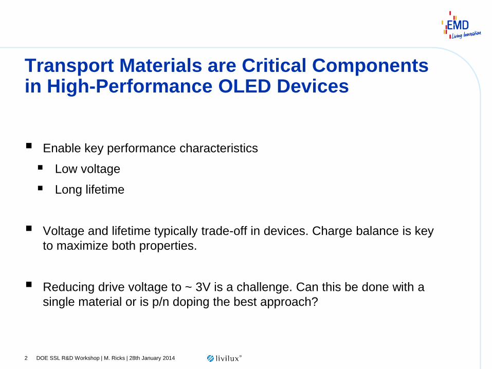
Transport Materials are Critical Components in High-Performance OLED Devices
Enable key performance characteristics
Low voltage
Long lifetime
Voltage and lifetime typically trade-off in devices. Charge balance is key
to maximize both properties.
Reducing drive voltage to ~ 3V is a challenge. Can this be done with a
single material or is p/n doping the best approach?
DOE SSL R&D Workshop | M. Ricks | 28th January 2014 2
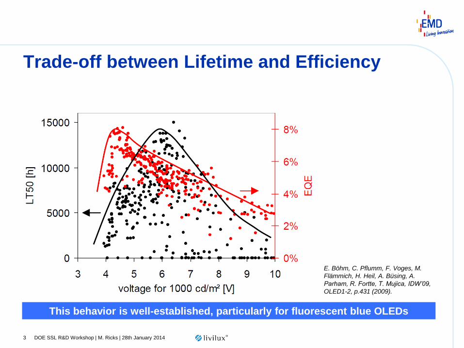
Trade-off between Lifetime and Efficiency
DOE SSL R&D Workshop | M. Ricks | 28th January 2014 3
E. Böhm, C. Pflumm, F. Voges, M.
Flämmich, H. Heil, A. Büsing, A.
Parham, R. Fortte, T. Mujica, IDW’09,
OLED1-2, p.431 (2009).
This behavior is well-established, particularly for fluorescent blue OLEDs
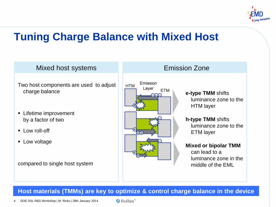
Tuning Charge Balance with Mixed Host
DOE SSL R&D Workshop | M. Ricks | 28th January 2014 4
Mixed host systems
Emission Zone
Two host components are used to adjust
charge balance
Lifetime improvement
by a factor of two
Low roll-off
Low voltage
compared to single host system
e-type TMM shifts
luminance zone to the
HTM layer
h-type TMM shifts
luminance zone to the
ETM layer
Mixed or bipolar TMM
can lead to a
luminance zone in the
middle of the EML
Host materials (TMMs) are key to optimize & control charge balance in the device
Tuning Charge Balance with Mixed Host
DOE SSL R&D Workshop | M. Ricks | 28th January 2014 5
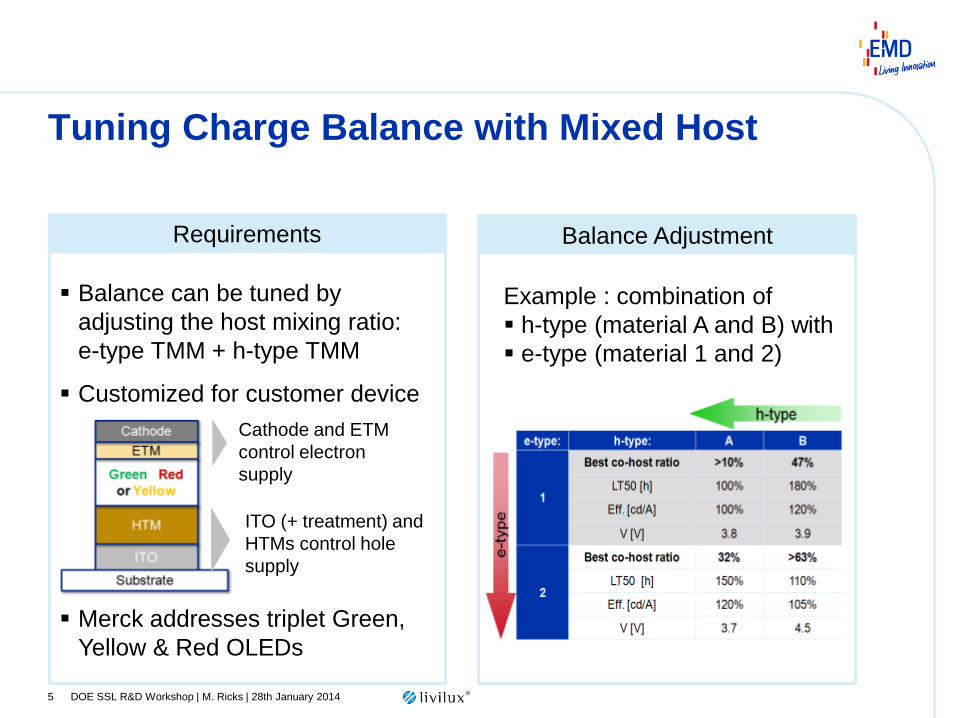
Balance can be tuned by
adjusting the host mixing ratio:
e-type TMM + h-type TMM
Customized for customer device
Merck addresses triplet Green,
Yellow & Red OLEDs
Cathode and ETM
control electron
supply
ITO (+ treatment) and
HTMs control hole
supply
Balance Adjustment Requirements
Example : combination of
h-type (material A and B) with
e-type (material 1 and 2)
c
Charge Balance Optimization through the Introduction of an HBL
DOE SSL R&D Workshop | M. Ricks | 28th January 2014 6
Lifetime and efficiency are further improved with the introduction of an HBL
Cathode
ETL
HBL
EML
HTL
HIL
ITO
0
10
20
30
40
50
60
70
80
Eff
icie
ncy [
cd
/A]
increasing hole transport
HBL
no HBL
0
50000
100000
150000
200000
LT
50 @
1000cd
/m²
[h
]
increasing hole transport
HBL
no HBL
GREEN
With a hole-rich EML mixture, we need to adjust the charge balance by
introducing an HBL
~ 70 cd/A
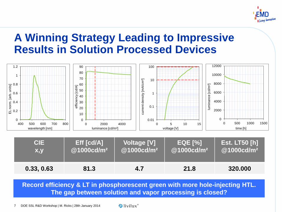
A Winning Strategy Leading to Impressive Results in Solution Processed Devices
DOE SSL R&D Workshop | M. Ricks | 28th January 2014 7
CIE
x,y
Eff [cd/A]
@1000cd/m²
Voltage [V]
@1000cd/m²
EQE [%]
@1000cd/m²
Est. LT50 [h]
@1000cd/m²
0.33, 0.63 81.3 4.7 21.8 320.000
0
2000
4000
6000
8000
10000
12000
0 500 1000 1500
lum
ina
nce
[cd
/m²]
time [h]
0
10
20
30
40
50
60
70
80
90
0 2000 4000
eff
icie
ncy [cd
/A]
luminance [cd/m²]
0.01
0.1
1
10
100
0 5 10 15
cu
rre
nt d
en
sity [m
A/c
m²]
voltage [V]
0
0.2
0.4
0.6
0.8
1
1.2
400 500 600 700 800
EL n
orm
. [a
rb. u
nits]
wavelength [nm]
Record efficiency & LT in phosphorescent green with more hole-injecting HTL.
The gap between solution and vapor processing is closed?
Charge Balance Optimization
DOE SSL R&D Workshop | M. Ricks | 28th January 2014 8
life
tim
e
Driving voltage
GREEN
RED
more electron
transport
life
tim
e
Driving voltage
GREEN
RED
more hole injection
Introduction of more hole-injecting transport layers significantly improves lifetime
Adding more electron
transportting materials to EML
mixtures results in lower voltage,
but reduced lifetime
Not enough holes to
counterbalance the electrons!
For a given EML mixture, vary the
hole injection properties of the
HTL.
HTL with strong hole injection
can improve voltage and lifetime
simultaneously!
Performance Progress – Solution Processing
DOE SSL R&D Workshop | M. Ricks | 28th January 2014 9
Triplet Green Triplet Red
Huge performance improvement with new materials in optimized devices
0
25
50
75
100
125
0 5 10 15
LT
50
[k
h]@
10
00
cd
/m²
eff. [cd/A]@1000 cd/m²
simple
device
with ETL
0
50
100
150
200
250
300
350
0 25 50 75
LT
50
[k
h]@
10
00
cd
/m²
eff. [cd/A]@1000 cd/m²
simple
device
with ETL Al
ETL
HBL
EML
HTL
HIL
ITO
evaporated
solution-
processed
Novel HTMs with Electron Blocking Capability
DOE SSL R&D Workshop | M. Ricks | 28th January 2014 10
HTM CIE x/y
Efficiency
[cd/A] @
1000 cd/m²
Voltage [V]
@
1000 cd/cm²
EQE [%] @
2000 cd/m²
LT50 [h] @
1000 cd/m² (based on n=2)
HTM-081 0.14/0.14 9.2 4.1 8.4 21 000
New HTM 0.13/0.14 13.2 4.1 11.6 44 000
Cathode
ETL
S-Blue EML
New HTM
HTM-081
HIL
ITO
Further improvement compared to HTM-081 based device
EMD / Merck have developed a variety of new HTMs, for use as hole
transporting layers with high triplet level & electron blocking capability
New stack configurations provide excellent lifetime, efficiency and voltage for
fluorescent & phosphorescent devices
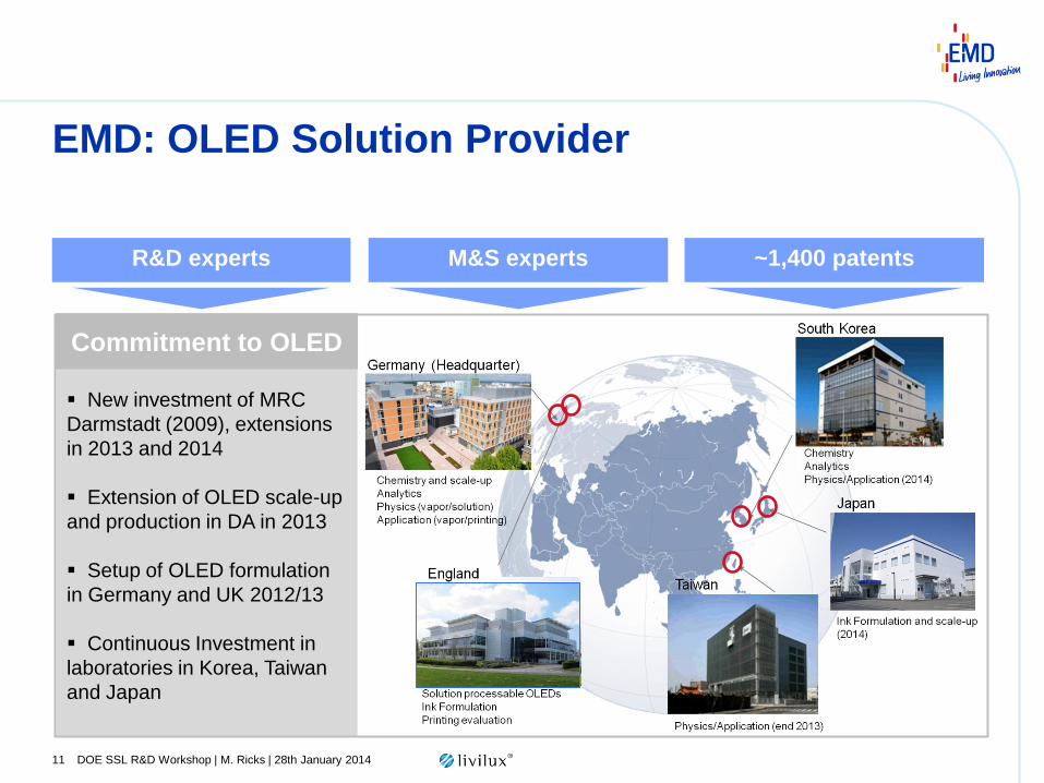
New investment of MRC
Darmstadt (2009), extensions
in 2013 and 2014
Extension of OLED scale-up
and production in DA in 2013
Setup of OLED formulation
in Germany and UK 2012/13
Continuous Investment in
laboratories in Korea, Taiwan
and Japan
Commitment to OLED
EMD: OLED Solution Provider
DOE SSL R&D Workshop | M. Ricks | 28th January 2014 11