Charge carrier dynamics in organic semiconductors and their donor- acceptor composites: Numerical modeling of time-resolved photocurrent Brian Johnson, Mark J. Kendrick, and Oksana Ostroverkhova Citation: J. Appl. Phys. 114, 094508 (2013); doi: 10.1063/1.4820259 View online: http://dx.doi.org/10.1063/1.4820259 View Table of Contents: http://jap.aip.org/resource/1/JAPIAU/v114/i9 Published by the AIP Publishing LLC. Additional information on J. Appl. Phys. Journal Homepage: http://jap.aip.org/ Journal Information: http://jap.aip.org/about/about_the_journal Top downloads: http://jap.aip.org/features/most_downloaded Information for Authors: http://jap.aip.org/authors
Transcript
Charge carrier dynamics in organic semiconductors and their donor-acceptor composites: Numerical modeling of time-resolved photocurrentBrian Johnson, Mark J. Kendrick, and Oksana Ostroverkhova Citation: J. Appl. Phys. 114, 094508 (2013); doi: 10.1063/1.4820259 View online: http://dx.doi.org/10.1063/1.4820259 View Table of Contents: http://jap.aip.org/resource/1/JAPIAU/v114/i9 Published by the AIP Publishing LLC. Additional information on J. Appl. Phys.Journal Homepage: http://jap.aip.org/ Journal Information: http://jap.aip.org/about/about_the_journal Top downloads: http://jap.aip.org/features/most_downloaded Information for Authors: http://jap.aip.org/authors
Charge carrier dynamics in organic semiconductors and theirdonor-acceptor composites: Numerical modeling of time-resolvedphotocurrent
Brian Johnson, Mark J. Kendrick, and Oksana Ostroverkhovaa)
Department of Physics, Oregon State University, Corvallis, Oregon 97331, USA
(Received 2 July 2013; accepted 18 August 2013; published online 4 September 2013)
We present a model that describes nanosecond (ns) time-scale photocurrent dynamics in
functionalized anthradithiophene (ADT) films and ADT-based donor-acceptor (D/A) composites.
By fitting numerically simulated photocurrents to experimental data, we quantify contributions of
multiple pathways of charge carrier photogeneration to the photocurrent, as well as extract
parameters that characterize charge transport (CT) in organic films including charge carrier
mobilities, trap densities, hole trap depth, and trapping and recombination rates. In pristine ADT
films, simulations revealed two competing charge photogeneration pathways: fast, occurring on
picosecond (ps) or sub-ps time scales with efficiencies below 10%, and slow, which proceeds at
the time scale of tens of nanoseconds, with efficiencies of about 11%–12%, at the applied electric
fields of 40–80 kV/cm. The relative contribution of these pathways to the photocurrent was
electric field dependent, with the contribution of the fast process increasing with applied electric
field. However, the total charge photogeneration efficiency was weakly electric field dependent
exhibiting values of 14%–20% of the absorbed photons. The remaining 80%–86% of the
photoexcitation did not contribute to charge carrier generation at these time scales. In ADT-based
D/A composites with 2 wt.% acceptor concentration, an additional pathway of charge
photogeneration that proceeds via CT exciton dissociation contributed to the total charge
photogeneration. In the composite with the functionalized pentacene (Pn) acceptor, which
exhibits strong exciplex emission from a tightly bound D/A CT exciton, the contribution of the
CT state to charge generation was small, �8%–12% of the total number of photogenerated
charge carriers, dependent on the electric field. In contrast, in the composite with PCBM
acceptor, the CT state contributed about a half of all photogenerated charge carriers. In both D/A
composites, the charge carrier mobilities were reduced and trap densities and average trap depths
were increased, as compared to a pristine ADT donor film. A considerably slower recombination
of free holes with trapped electrons was found in the composite with the PCBM acceptor, which
led to slower decays of the transient photocurrent and considerably higher charge retention,
as compared to a pristine ADT donor film and the composite with the functionalized Pn acceptor.VC 2013 AIP Publishing LLC. [http://dx.doi.org/10.1063/1.4820259]
I. INTRODUCTION
Organic donor-acceptor (D/A) composites are of interest
for applications in solar cells,1 lasers,2 photodetectors,3,4 and
photorefractive devices5 due to enhanced charge carrier pho-
togeneration resulting from the photoinduced charge transfer
(CT) between the donor (D) and acceptor (A) molecules.
While currently most high-performance bulk heterojunctions
(BHJs) are based on polymer/fullerene composites, perform-
ance of small-molecule BHJs (SMBHJs), which are still
relatively unexplored, is rapidly improving,6 with several
SMBHJ-based solar cells exhibiting power conversion
efficiencies of 6%–7%.7,8 In order to further improve per-
formance of BHJs, including SMBHJs, it is important to
understand mechanisms of charge carrier photogeneration,
transport, and recombination, as well as their contribution to
the photocurrent, in both pristine organic semiconductor
materials and their D/A composites. Many recent studies
have addressed dynamics and propensity for dissociation of
CT states,9–19 effects of D/A LUMO and HOMO energy
offsets,20–24 and of D/A molecular packing at the D/A inter-
faces,25 in polymer-based BHJs, whereas relatively few
studies have explored similar issues in SMBHJs.26–30 For
SMBHJs, of particular interest are solution-processable pho-
toconductive organic semiconductors with high charge
carrier mobilities and solid-state packing favoring efficient
charge separation at the D/A interfaces.31 Examples of such
materials are functionalized pentacene (Pn) and anthradithio-
phene (ADT) derivatives which exhibit thin-film charge
carrier (hole) mobilities of above �1.5 cm2/(Vs), fast photo-
response, high photoconductivity under continuous wave
(cw) excitation,32–34 and a variety of solid-state packing
motifs controlled by functionalization of the molecules.35
Investigation of mechanisms of charge photogeneration and
transport in such materials and their D/A composites is the
focus of this paper.
One of the difficulties in establishing physical mecha-
nisms of photoexcited charge carrier dynamics in organica)Electronic mail: [email protected]
composite. Insets illustrate effects of different charge generation pathway
choices and show best fits to the data obtained using: (a) at 60 kV/cm, SSC
generation pathway 1 only (dashed line), FE dissociation pathway 2 only
(dashed-dotted line), both pathways (solid line); (b) at 60 kV/cm and (c) at
40 kV/cm: FE dissociation pathway 2 only (dashed-dotted line), combined
SSC and FE dissociation pathways 1 and 2, respectively (dashed line), and
combined SSC, FE dissociation, and CT exciton dissociation pathways 1, 2,
and 4, respectively (solid line).
094508-5 Johnson, Kendrick, and Ostroverkhova J. Appl. Phys. 114, 094508 (2013)
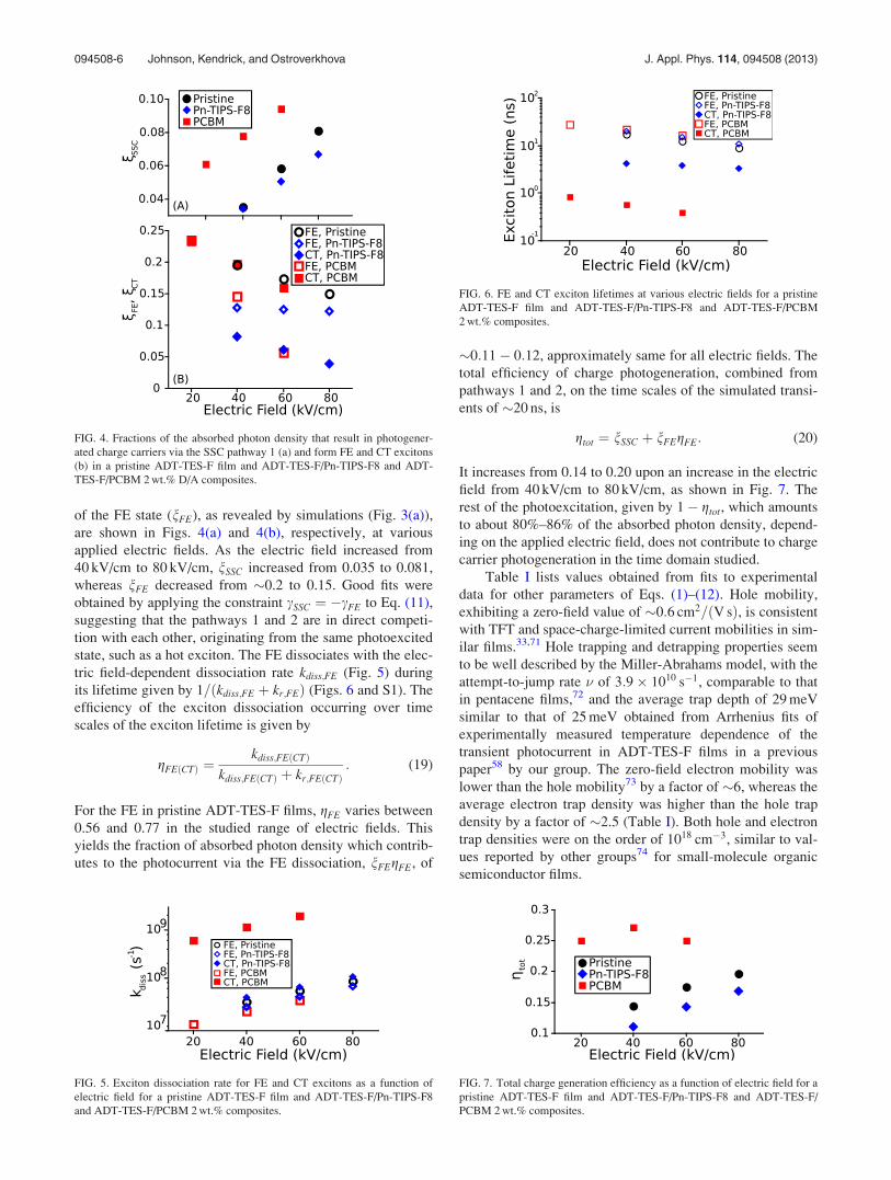
of the FE state (nFE), as revealed by simulations (Fig. 3(a)),
are shown in Figs. 4(a) and 4(b), respectively, at various
applied electric fields. As the electric field increased from
40 kV/cm to 80 kV/cm, nSSC increased from 0.035 to 0.081,
whereas nFE decreased from �0.2 to 0.15. Good fits were
obtained by applying the constraint cSSC ¼ �cFE to Eq. (11),
suggesting that the pathways 1 and 2 are in direct competi-
tion with each other, originating from the same photoexcited
state, such as a hot exciton. The FE dissociates with the elec-
tric field-dependent dissociation rate kdiss;FE (Fig. 5) during
its lifetime given by 1=ðkdiss;FE þ kr;FEÞ (Figs. 6 and S1). The
efficiency of the exciton dissociation occurring over time
scales of the exciton lifetime is given by
gFEðCTÞ ¼kdiss;FEðCTÞ
kdiss;FEðCTÞ þ kr;FEðCTÞ: (19)
For the FE in pristine ADT-TES-F films, gFE varies between
0.56 and 0.77 in the studied range of electric fields. This
yields the fraction of absorbed photon density which contrib-
utes to the photocurrent via the FE dissociation, nFEgFE, of
�0:11� 0:12, approximately same for all electric fields. The
total efficiency of charge photogeneration, combined from
pathways 1 and 2, on the time scales of the simulated transi-
ents of �20 ns, is
gtot ¼ nSSC þ nFEgFE: (20)
It increases from 0.14 to 0.20 upon an increase in the electric
field from 40 kV/cm to 80 kV/cm, as shown in Fig. 7. The
rest of the photoexcitation, given by 1� gtot, which amounts
to about 80%–86% of the absorbed photon density, depend-
ing on the applied electric field, does not contribute to charge
carrier photogeneration in the time domain studied.
Table I lists values obtained from fits to experimental
data for other parameters of Eqs. (1)–(12). Hole mobility,
exhibiting a zero-field value of �0:6 cm2=ðV sÞ, is consistent
with TFT and space-charge-limited current mobilities in sim-
ilar films.33,71 Hole trapping and detrapping properties seem
to be well described by the Miller-Abrahams model, with the
attempt-to-jump rate � of 3:9� 1010 s�1, comparable to that
in pentacene films,72 and the average trap depth of 29 meV
similar to that of 25 meV obtained from Arrhenius fits of
experimentally measured temperature dependence of the
transient photocurrent in ADT-TES-F films in a previous
paper58 by our group. The zero-field electron mobility was
lower than the hole mobility73 by a factor of �6, whereas the
average electron trap density was higher than the hole trap
density by a factor of �2.5 (Table I). Both hole and electron
trap densities were on the order of 1018 cm�3, similar to val-
ues reported by other groups74 for small-molecule organic
semiconductor films.
FIG. 4. Fractions of the absorbed photon density that result in photogener-
ated charge carriers via the SSC pathway 1 (a) and form FE and CT excitons
(b) in a pristine ADT-TES-F film and ADT-TES-F/Pn-TIPS-F8 and ADT-
TES-F/PCBM 2 wt.% D/A composites.
FIG. 5. Exciton dissociation rate for FE and CT excitons as a function of
electric field for a pristine ADT-TES-F film and ADT-TES-F/Pn-TIPS-F8
and ADT-TES-F/PCBM 2 wt.% composites.
FIG. 6. FE and CT exciton lifetimes at various electric fields for a pristine
ADT-TES-F film and ADT-TES-F/Pn-TIPS-F8 and ADT-TES-F/PCBM
2 wt.% composites.
FIG. 7. Total charge generation efficiency as a function of electric field for a
pristine ADT-TES-F film and ADT-TES-F/Pn-TIPS-F8 and ADT-TES-F/
PCBM 2 wt.% composites.
094508-6 Johnson, Kendrick, and Ostroverkhova J. Appl. Phys. 114, 094508 (2013)
B. D/A composites
The model that takes into account the SSC and FE chan-
nels of carrier photogeneration produced good fits for the
pristine ADT-TES-F film photocurrents, but it was unable to
accurately replicate some of the more complicated dynamics
of photocurrents from composites. The insets of Figs. 3(b)
and 3(c) show the best results of fitting the photocurrent at
the electric fields of 60 kV/cm and 40 kV/cm in the ADT-
TES-F/Pn-TIPS-F8 and ADT-TES-F/PCBM composites,
respectively, with the models that include FE dissociation-
only (dashed-dotted line, pathway 2 in Fig. 2) and both the
SSC and FE dissociation pathways (dashed line, pathways 1
and 2, respectively, in Fig. 2). In addition, there was little
consistency in the fits across the studied electric field range,
and our multiple-electric-field fitting process was unable to
replicate the correct electric field dependence of the transi-
ents. Our previous work27 identified a possibility of charge
generation via CT exciton dissociation in several D/A com-
posites with the ADT-TES-F donor, with a CT exciton that
may or may not be detectable by PL measurements, depend-
ing on the acceptor. For example, in the ADT-TES-F/Pn-
TIPS-F8 D/A composite, an exciplex that formed between
the donor HOMO and the acceptor LUMO was detected by
the PL emission and was considered as a potential contribu-
tor of charge carriers via exciplex dissociation. In contrast,
in the ADT-TES-F/PCBM D/A composite, no exciplex emis-
sion was detected; however, based on the photocurrent
dynamics and partial quenching of the ADT-TES-F donor
PL, it was inferred that there might exist dark CT states that
form between the ADT-TES-F donor and PCBM acceptor,
which could contribute to charge carrier generation.
Based on these considerations, to accurately reproduce
the photocurrent dynamics in the composites with the
Pn-TIPS-F8 and PCBM acceptors, we added the charge gen-
eration pathway 4 in Fig. 2, which proceeds via CT exciton
dissociation, to the set of equations (Eq. (5)) and additional
terms to Eqs. (1) and (3). To describe CT exciton dissocia-
tion, we used the Onsager-Braun model, similar to that of the
FE dissociation, but with a different initial pair separation
aCT and recombination rate kr;CT . Thus, in D/A composites,
there are three competing channels of charge photogenera-
tion: the fast SSC pathway, FE dissociation, and CT exciton
dissociation (pathways 1, 2, and 4, respectively, in Fig. 2),
with relative contribution of each pathway to the overall
charge photogeneration being electric field dependent. Since
the exact pathway of the CT state formation is unknown,26,58
we did not impose restrictions on the relative values of
cSSC; cFE, and cCT in Eq. (11). Following the same fitting
process as described above, we fit the experimental data to
the simulated photocurrent transients (Fig. 3). The addition
of the CT exciton dissociation improved the goodness-of-fit
ratings for the fits to the data from the composite films
(Figs. 3(b) and 3(c)). The fit to the data from the composite
with the PCBM acceptor at an applied electric field of
60 kV/cm was lower in quality than the fits to the data at
lower electric fields due to breaking down of the assumption
of Eq. (11) at higher electric fields. As in pristine ADT-TES-
F films, in both D/A composites under consideration, the
efficiency of fast carrier generation via the SSC pathway was
below 10% (Fig. 4(a)).
In the composite with the Pn-TIPS-F8 acceptor, �0.12
(�0.04–0.08) of the absorbed photon density Nph formed
the charge-generating FE (CT exciton) (Fig. 4(b)). These
dissociated during their lifetimes (Figs. 6 and S1) with the
electric field dependent efficiency gFE ðgCTÞ, calculated using
Eq. (19), of 0.49–0.72 (0.17–0.35) in the studied range of
electric fields. This yields a fraction of Nph contributing to
the overall charge photogeneration via the FE (CT exciton)
dissociation pathway, nFEgFE ðnCTgCTÞ, of 0.062–0.088
(0.014–0.015). The contribution of the CT dissociation to
charge carrier generation in this composite, given by
nCTgCT=gtot, is the lowest of the three contributing pathways
at 8%–12%, which is consistent with our previous observa-
tion of a strong PL emission from the ADT-TES-F/Pn-TIPS-
F8 CT state (exciplex), indicative of a tightly bound CT state
with a relatively low dissociation rate kdiss;CT (Fig. 5).27 The
total fraction of the absorbed photon density which results in
charge carrier photogeneration at time scales of �20 ns, is
gtot ¼ nSSC þ nFEgFE þ nCTgCT : (21)
It increases slightly, from �0.11 to �0.17, as the electric
field increases from 40 kV/cm to 80 kV/cm (Fig. 7). The rest
of the photoexcitation, given by 1� gtot, which amounts to
�83%–89% of the absorbed photons, does not contribute to
charge carrier photogeneration in the time domain studied.
In the composite with the PCBM acceptor, the CT exci-
ton formed considerably more efficiently (nCT in Fig. 4(b))
and was considerably more prone to dissociation as com-
pared to that in the composite with the Pn-TIPS-F8 acceptor.
As a result, the contribution of the CT exciton dissociation
(pathway 4) into the overall charge photogeneration, nCTgCT ,
of 0.12–0.13 (i.e., 12%–13%) of the absorbed photon density
was a factor of �8.5 larger than that in the ADT-TES-F/Pn-
TIPS-F8 composite. It also dominated over the pathway 2
TABLE I. Parameter values extracted from experimental data for pristine
ADT-TES-F films and ADT-TES-F-based D/A composites with Pn-TIPS-F8
and PCBM acceptors using simulation with a system of Eqs. (1)–(12).
Parameter descriptions are given in the text.
Parameter (unit) ADT-TES-F 2% Pn-TIPS-F8 2% PCBM
ln;0 ðcm2ðV sÞ�1Þ 0.093 0.016 0.025
lp;0 ðcm2ðV sÞ�1Þ 0.60 0.51 0.36
cn ðcm=VÞ1=21:8� 10�3 2:0� 10�3 3:8� 10�3
cp ðcm=VÞ1=23:1� 10�4 6:0� 10�4 9:1� 10�4
D (meV) 29 41 39
Nn ðcm�3Þ 7:1� 1018 7:4� 1018 8:7� 1019
Np ðcm�3Þ 2:8� 1018 2:2� 1018 3:8� 1018
BnNn ðs�1Þ 5:1� 1011 8:9� 1011 7:8� 1011
BpNp ðs�1Þ 3:9� 1010 6:9� 1010 2:1� 1011
Bnf pt ðcm3s�1Þ 1:4� 10�3 5:0� 10�3 4:0� 10�3
Bpf ntðcm3s�1Þ 2:1� 10�5 2:7� 10�5 8:2� 10�7
aFE (nm) 1.18 1.18 1.18
aCT (nm) … 1.22 1.77
094508-7 Johnson, Kendrick, and Ostroverkhova J. Appl. Phys. 114, 094508 (2013)
(charge generation via FE dissociation), especially at low
electric fields, which converted nFEgFE ¼ 0:03� 0:07 (i.e.,
3%–7%) of the absorbed photons into charge carriers.
Table I summarizes other parameters pertaining to
charge generation and transport in the studied D/A compo-
sites. In both composites, the hole and electron mobilities
were reduced as compared to those in pristine ADT-TES-F
films, whereas the average trap densities were increased; this
result is expected, given our effective medium approach to
charge transport modeling in these composites with low
acceptor concentration. In both composites, the effective
hole trap depth was increased with respect to that in pristine
ADT-TES-F films (41 and 39 meV in the composites with
Pn-TIPS-F8 and PCBM, respectively), due to an increased
disorder in the composite films.
V. DISCUSSION
Figure 8 summarizes the distribution of the photoexcita-
tion among various pathways for the pristine ADT-TES-F
films and ADT-TES-F/Pn-TIPS-F8 and ADT-TES-F/PCBM
composites at low acceptor concentrations, obtained from
simulations of the photocurrents over �20 ns, at the applied
electric field of 40 kV/cm. In pristine ADT-TES-F films at
this field, the contribution of the pathway 2 (FE dissociation)
to ns time-scales charge photogeneration was a factor of
�3.1 larger than that of the pathway 1. This dominance of the
pathway 2 progressively reduced as the electric field
increased. In ADT-TES-F/Pn-TIPS-F8 composites, the path-
way 2 dominated over the pathway 1 by a factor of �1.6,
whereas the contribution of the pathway 4 (CT exciton disso-
ciation) to the charge generation was a factor of �4.5 lower
than that of the pathway 2 and slightly decreased with the
electric field. In contrast, in ADT-TES-F/PCBM composites,
pathway 4 was the dominant factor, contributing about half
of all charge carriers ðnCTgCT=gtot � 0:49Þ, whereas the other
half was distributed between the pathways 1 and 2. The path-
way 4 contribution was weakly field dependent in the studied
range, whereas the trends in relative contributions of the path-
ways 1 and 2 followed those of pristine ADT-TES-F films.
Note that in spite of electric field dependence of various
parameters contributing to charge photogeneration, the total
charge photogeneration efficiency in ADT-TES-F/PCBM
composites (Fig. 7) is electric field independent in the studied
range of electric fields, similar to that reported in D/A sys-
tems with polymeric donors and PCBM acceptors.75,76
Ultrafast charge carrier photogeneration has been
observed in a variety of small-molecule and polymeric organic
semiconductors via ultrafast spectroscopy methods,26,77–79
Auston switch-based techniques,39,80,81 and fast oscilloscope
detection of photocurrents.33,54,82 In most cases, the efficiency
of this process is at or below �10%, in agreement with values
of nSSC (which dominates charge generation at fast time
scales) extracted from our simulations. Many of these methods
enable determination of the product of the sum of hole and
electron mobilities (ltot ¼ lp þ ln) and of the photogenera-
tion efficiency. In our films the ltotnSSC values (Fig. 4(a) and
Table I) are between �0.02 and 0:06 cm2=V s, in good agree-
ment with experimental observations from similar films.33,54,78
However, the mechanism of achieving the SSC state at ultra-
fast time scales in ADT films is unknown and requires further
investigation. Two main possibilities are direct band-to-band
excitations26 and hot exciton dissociation,56 with the electric
field dependence of the parameter nSSC observed here more
consistent with the latter process.
The simulations revealed that a FE with lifetimes on the
order of 10–20 ns (Figs. 6 and S1) contributes a considerable
number of charge carriers at ns time-scales through pathway
2 in Fig. 2. In the studied D/A composites, the FE lifetimes
were similar to those in the pristine ADT-TES-F film (Fig. 6),
which confirms that the FE state is formed on the ADT-TES-
F donor. There are several possible origins of such FE states.
For example, these could be dark states that are delocalized
over several ADT-TES-F molecules in the ADT-TES-F
H-aggregates,58 similar to those in H-aggregates of sexithio-
phene films.83 The pristine ADT-TES-F films and both D/A
composites considered here exhibit a relatively strong PL
from the relaxed ADT-TES-F excitons.27,58 The emissive
ADT-TES-F excitons at room temperature are highly mobile
within disordered ADT-TES-F H-aggregates, which shortens
their PL lifetimes from about 13 ns (for isolated molecules) to
1–2 ns (in films).58 Our previous work revealed that these
excitons do not contribute to photocurrents at ns time-scales
and cannot be the charge-generating FE states of Fig. 2.27,58
Instead, these are the excitons that constitute most of the
photoexcitation (�80% of absorbed photons) that does not
FIG. 8. Summary of distribution of the
total photoexcitation (100%) among var-
ious relaxation paths at an applied elec-
tric field of 40 kV/cm. Values are given
for a pristine ADT-TES-F film (A), an
ADT-TES-F/Pn-TIPS-F8 2 wt. % com-
posite film (B), and an ADT-TES-F/
PCBM 2 wt.% composite film (C).
Values in boxes are fractions n from
Fig. 4 multiplied by 100%, whereas val-
ues below the boxes are dissociation
efficiencies gFE;CT of Eq. (19), also mul-
tiplied by 100%.
094508-8 Johnson, Kendrick, and Ostroverkhova J. Appl. Phys. 114, 094508 (2013)
produce charge carriers. However, since the PL lifetimes of
the FE in Fig. 6 are close to PL lifetimes of isolated ADT-
TES-F molecules,33 the alternative assignment for the FE
states observed here could be relatively immobile ADT-TES-
F excitons, possibly formed at grain boundaries, which are
longer lived and have more time to dissociate as compared to
highly mobile excitons that constitute the majority of the
photoexcited species.58
The simulations established that the CT state in the
ADT-TES-F/Pn-TIPS-F8 composite, contributing to charge
photogeneration through pathway 4 in Fig. 2, exhibits life-
times of 3.4–4.5 ns (Fig. 6). These are close to experimen-
tally measured PL lifetimes of the exciplex (3.8–4.6 ns,
depending on the applied electric field) in this composite,
which suggests that the nature of the charge-generating CT
state in Fig. 2 is the exciplex whose properties we have
reported previously.27 Indeed, low contribution of the CT
states to the photocurrent in this composite is consistent with
a highly emissive tightly bound exciplex, in agreement with
experiments.27 The CT state in the composite with the
PCBM acceptor was found to exhibit considerably lower
lifetimes (Figs. 6 and S1) than those of the ADT-TES-F FE
and the CT in the composite with the Pn-TIPS-F8 acceptor.
Additionally, it was more dissociative than either of these
excitons (Fig. 5), which is consistent with a larger LUMO
offset between ADT-TES-F and PCBM and larger D/A sepa-
ration due to the size of the PCBM molecule as compared to
Pn-TIPS-F8, both of which factors have been shown to
enhance the photocurrent.27,84 Our simulations confirm the
latter statement, yielding the initial charge pair separation
aCT of 1.77 nm in the ADT-TES-F/PCBM composite, as
compared to that of 1.22 nm in the ADT-TES-F/Pn-TIPS-F8
composite.
The total amount of charge generated at ns time-scales,
0.1–0.25 of absorbed photon density (Fig. 7), only differs
by a factor of �2 in all three systems under study, with the
highest in the composite with the PCBM acceptor followed
by pristine ADT-TES-F film and the composite with the
Pn-TIPS-F8 acceptor, consistent with our previous observa-
tions.27 However, our previous studies27 also established that
the amount of mobile charge over the period of 1 ls,
obtained by integrating transient photocurrents over this time
period, as well as photocurrents obtained under cw illumina-
tion, are considerably higher (by a factor of �6–10) in the
composite with the PCBM acceptor as compared to pristine
ADT-TES-F films. Based on our simulation results, this is
due to a considerably lower rate of recombination between
trapped electrons and free holes in the ADT-TES-F/PCBM
composite (Bpf ntin Table I and Fig. S2), which results in a
significantly slower decay of the photocurrent in this com-
posite, and thus, higher charge retention, as compared to that
in pristine ADT-TES-F films.
VI. CONCLUSIONS
We presented a model based on drift conduction which
enabled us to quantify contributions of multiple pathways to
charge carrier photogeneration, as well as extract parameters
that characterize charge transport in pristine organic films
and organic D/A composites from transient photocurrents. In
pristine ADT-TES-F films, simulations revealed two compet-
ing charge photogeneration pathways: fast charge genera-
tion, on a ps or sub-ps time scale, with efficiencies below
10%, and slow, on the time scale of tens of nanoseconds,
with efficiencies of about 11%–12%, at the applied electric
fields of 40–80 kV/cm. The relative contribution of these
pathways to the photocurrent was electric field dependent,
with the contribution of the fast process increasing with
applied electric field. However, the total charge photogenera-
tion efficiency was weakly electric field dependent exhibit-
ing values of 14%–20% of the absorbed photon density. The
remaining 80%–86% of the photoexcitation did not contrib-
ute to charge carrier generation at these time scales. In ADT-
TES-F-based D/A composites, an additional pathway of
charge photogeneration that proceeds via CT exciton dissoci-
ation contributed to the total charge photogeneration. In the
composite with the 2 wt.% Pn-TIPS-F8 acceptor, which
exhibits strong exciplex emission from a tightly bound D/A
CT exciton, the contribution of the CT state to charge gener-
ation was small, �8%–12% of the total number of photogen-
erated charge carriers, dependent on the electric field. In
contrast, in the composite with 2 wt.% PCBM acceptor, the
CT state contributed about a half of all photogenerated
charge carriers. In both D/A composites, the charge carrier
mobilities were reduced and trap densities and average trap
depths were increased, as compared to a pristine ADT-TES-
F donor film. A considerably slower recombination of free
holes with trapped electrons was found in the composite
with the PCBM acceptor, which led to slower decays of the
transient photocurrent and considerably higher charge reten-
tion, as compared to a pristine ADT-TES-F donor film and
the composite with the Pn-TIPS-F8 acceptor.
ACKNOWLEDGMENTS
We thank Professor J. E. Anthony for ADT-TES-F and
Pn-TIPS-F8. This work was supported by the NSF Grant
Nos. DMR-0748671 (via CAREER program) and DMR-
1207309.
1A. J. Heeger, Chem. Soc. Rev. 39, 2354 (2010).2I. D. W. Samuel and G. A. Turnbull, Chem. Rev. 107, 1272 (2007).3Y. Kim, M. Ballarotto, D. Park, M. Du, W. Cao, C. H. Lee, W. N.
Herman, and D. B. Romero, Appl. Phys. Lett. 91, 193510 (2007).4S. Moller, S. Forrest, C. Perlov, W. Jackson, and C. Taussig, J. Appl.
Phys. 94, 7811 (2003).5O. Ostroverkhova and W. E. Moerner, Chem. Rev. 104, 3267 (2004).6B. Walker, C. Kim, and T.-Q. Nguyen, Chem. Mater. 23, 470 (2011).7Y. Sun, G. C. Welch, W. L. Leong, C. J. Takacs, G. C. Bazan, and A. J.
Heeger, Nature Mater. 11, 44 (2012).8A. Mishra and P. B€auerle, Ang. Chem. 124, 2060 (2012).9A. A. Bakulin, A. Rao, V. G. Pavelyev, P. H. M. van Loosdrecht, M. S.
Pshenichnikov, D. Niedzialek, J. Cornil, D. Beljonne, and R. H. Friend,
Science 335, 1340 (2012).10S. Singh, B. Pandit, T. P. Basel, S. Li, D. Laird, and Z. V. Vardeny, Phys.
Rev. B 85, 205206 (2012).11G. Sliau�zys, K. Arlauskas, and V. Gulbinas, Phys. Status Solidi A 209,
1302 (2012).12P. E. Schwenn, K. Gui, Y. Zhang, P. L. Burn, P. Meredith, and B. J.
Powell, Org. Electron. 13, 2538 (2012).13G. Grancini, M. Maiuri, D. Fazzi, A. Petrozza, H.-J. Egelhaaf, D. Brida,
G. Cerullo, and G. Lanzani, Nature Mater. 12, 29 (2012).
094508-9 Johnson, Kendrick, and Ostroverkhova J. Appl. Phys. 114, 094508 (2013)
14K. Aryanpour, D. Psiachos, and S. Mazumdar, Phys. Rev. B 81, 085407
(2010).15M. Mingebach, S. Walter, V. Dyakonov, and C. Deibel, Appl. Phys. Lett.
100, 193302 (2012).16R. D. Pensack and J. B. Asbury, Chem. Phys. Lett. 515, 197 (2011).17F. Etzold, I. A. Howard, R. Mauer, M. Meister, T.-D. Kim, K.-S. Lee,
N. S. Baek, and F. Laquai, J. Am. Chem. Soc. 133, 9469 (2011).18M. A. Faist, T. Kirchartz, W. Gong, R. S. Ashraf, I. McCulloch, J. C. de
Mello, N. J. Ekins-Daukes, D. D. C. Bradley, and J. Nelson, J. Am. Chem.
Soc. 134, 685 (2012).19A. E. Jailaubekov, A. P. Willard, J. R. Tritsch, W.-L. Chan, N. Sai, R.
Gearba, L. G. Kaake, K. J. Williams, K. Leung, P. J. Rossky, and X.-Y.
Zhu, Nature Mater. 12, 66 (2013).20S. D. Dimitrov, A. A. Bakulin, C. B. Nielsen, B. C. Schroeder, J. Du, H.
Bronstein, I. McCulloch, R. H. Friend, and J. R. Durrant, J. Am. Chem.
Soc. 134, 18189 (2012).21A. A. Bakulin, S. D. Dimitrov, A. Rao, P. C. Y. Chow, C. B. Nielsen,
B. C. Schroeder, I. McCulloch, H. J. Bakker, J. R. Durrant, and R. H.
Friend, J. Phys. Chem. Lett 4, 209 (2013).22W. Zhang, Y.-W. Wang, R. Hu, L.-M. Fu, X.-C. Ai, J.-P. Zhang, and J.-H.
Hou, J. Phys. Chem. C 117, 735 (2013).23G. Ren, C. W. Schlenker, E. Ahmed, S. Subramaniyan, S. Olthof, A. Kahn,
D. S. Ginger, and S. A. Jenekhe, Adv. Funct. Mater. 23, 1238 (2013).24D. H. K. Murthy, M. Gao, M. J. W. Vermeulen, L. D. A. Siebbeles, and
T. J. Savenije, J. Phys. Chem. C 116, 9214 (2012).25T. W. Holcombe, J. E. Norton, J. Rivnay, C. H. Woo, L. Goris, C. Piliego,
G. Griffini, A. Sellinger, J.-L. Bredas, A. Salleo, and J. M. J. Frechet,
J. Am. Chem. Soc. 133, 12106 (2011).26L. G. Kaake, J. J. Jasieniak, R. C. Bakus, G. C. Welch, D. Moses, G. C.
Bazan, and A. J. Heeger, J. Am. Chem. Soc. 134, 19828 (2012).27M. J. Kendrick, A. Neunzert, M. M. Payne, B. Purushothaman, B. D.
Rose, J. E. Anthony, M. M. Haley, and O. Ostroverkhova, J. Phys. Chem.
C 116, 18108 (2012).28D. Credgington, F. C. Jamieson, B. Walker, T.-Q. Nguyen, and J. R.
Durrant, Adv. Mater. 24, 2135 (2012).29R. Fitzner, C. Elschner, M. Weil, C. Uhrich, C. Koerner, M. Riede, K.
Leo, M. Pfeiffer, E. Reinold, E. Mena-Osteritz, and P. Baeuerle, Adv.
Mater. 24, 675 (2012).30Y. S. Chung, N. Shin, J. Kang, Y. Jo, V. M. Prabhu, S. K. Satija, R. J.
Kline, D. M. DeLongchamp, M. F. Toney, M. A. Loth, B. Purushothaman,
J. E. Anthony, and D. Y. Yoon, J. Am. Chem. Soc. 133, 412 (2011).31Y.-F. Lim, Y. Shu, S. R. Parkin, J. E. Anthony, and G. G. Malliaras,
J. Mater. Chem. 19, 3049 (2009).32S. K. Park, D. A. Mourey, S. Subramanian, J. E. Anthony, and T. N.
Jackson, Appl. Phys. Lett. 93, 043301 (2008).33A. D. Platt, J. Day, S. Subramanian, J. E. Anthony, and O. Ostroverkhova,
J. Phys. Chem. C 113, 14006 (2009).34S. K. Park, T. N. Jackson, J. E. Anthony, and D. A. Mourey, Appl. Phys.
Lett. 91, 063514 (2007).35J. E. Anthony, Chem. Rev. 106, 5028 (2006).36H. van Eersel, R. A. J. Janssen, and M. Kemerink, Adv. Funct. Mater. 22,
2700 (2012).37M. C. Heiber and A. Dhinojwala, J. Chem. Phys. 137, 014903 (2012).38J. Nelson, Phys. Rev. B 67, 155209 (2003).39C. Soci, D. Moses, Q.-H. Xu, and A. Heeger, Phys. Rev. B 72, 245204 (2005).40L. Kulikovsky, D. Neher, E. Mecher, K. Meerholz, H.-H. H€orhold, and O.
Ostroverkhova, Phys. Rev. B 69, 125216 (2004).41O. Ostroverkhova and K. D. Singer, J. Appl. Phys. 92, 1727 (2002).42I. Hwang, C. R. McNeill, and N. C. Greenham, J. Appl. Phys. 106, 094506
Horng, J. Appl. Phys. 107, 084503 (2010).44L. Koster, E. Smits, V. Mihailetchi, and P. Blom, Phys. Rev. B 72, 085205
(2005).45T. Kirchartz, B. E. Pieters, K. Taretto, and U. Rau, Phys. Rev. B 80,
035334 (2009).46A. Petersen, A. Ojala, T. Kirchartz, T. Wagner, F. W€urthner, and U. Rau,
Phys. Rev. B 85, 245208 (2012).47W. E. B. Shepherd, A. D. Platt, M. J. Kendrick, M. A. Loth, J. E. Anthony,
and O. Ostroverkhova, J. Phys. Chem. Lett. 2, 362 (2011).48W. E. B. Shepherd, A. D. Platt, D. Hofer, O. Ostroverkhova, M. Loth, and
J. E. Anthony, Appl. Phys. Lett. 97, 163303 (2010).
49Y. Shang, Q. Li, L. Meng, D. Wang, and Z. Shuai, Theor. Chem. Acc.
129, 291 (2011).50K. Maturova, M. Kemerink, M. M. Wienk, D. S. H. Charrier, and R. A. J.
Janssen, Adv. Funct. Mater. 19, 1379 (2009).51C. Deibel, A. Wagenpfahl, and V. Dyakonov, Phys. Status Solidi (RRL) 2,
175 (2008).52E. Knapp, R. H€ausermann, H. U. Schwarzenbach, and B. Ruhstaller,
J. Appl. Phys. 108, 054504 (2010).53W. Tress, K. Leo, and M. Riede, Phys. Rev. B 85, 155201 (2012).54J. Day, S. Subramanian, J. E. Anthony, Z. Lu, R. J. Twieg, and O.
Ostroverkhova, J. Appl. Phys. 103, 123715 (2008).55J. Day, A. D. Platt, S. Subramanian, J. E. Anthony, and O. Ostroverkhova,
J. Appl. Phys. 105, 103703 (2009).56V. Arkhipov, E. Emelianova, and H. B€assler, Phys. Rev. Lett. 82, 1321
(1999).57J. D. Servaites, B. M. Savoie, J. B. Brink, T. J. Marks, and M. A. Ratner,
Energy Environ. Sci. 5, 8343 (2012).58A. Platt, M. Kendrick, M. Loth, J. Anthony, and O. Ostroverkhova, Phys.
Rev. B 84, 235209 (2011).59C. Braun, J. Chem. Phys. 80, 4157 (1984).60K. Falkowski, W. Stampor, P. Grygiel, and W. Tomaszewicz, Chem.
Phys. 392, 122 (2012).61V. I. Arkhipov and H. B€assler, in Physics of Organic Semiconductors,
edited by W. Br€utting (Wiley-VCH Verlag GmbH & Co. KGaA, 2005).62J. Kalinowski, W. Stampor, and P. G. Di Marco, J. Chem. Phys. 96, 4136
(1992).63D. Wehenkel, L. Koster, M. Wienk, and R. Janssen, Phys. Rev. B 85,
125203 (2012).64G. Malliaras and J. Scott, J. Appl. Phys. 83, 5399 (1998).65See supplementary material at http://dx.doi.org/10.1063/1.4820259 for
details of the fitting process, the calculation of initial conditions, exciton
time-resolved dynamics, and simulated dependence of the photocurrent
dynamics on trap-assisted recombination.66S. Lacic and O. Ingan€as, J. Appl. Phys. 97, 124901 (2005).67J. Scott and G. Malliaras, Chem. Phys. Lett. 299, 115 (1999).68S. G. Johnson, The NLOPT non-linear optimization package, version 2.3,
2012, see www.ab-initio.mit.edu/nlopt.69T. Runarsson and X. Yao, IEEE Trans. Syst. Man. Cybern., Part C Appl.
Rev. 35, 233 (2005).70M. J. D. Powell, in Advances in Optimization and Numerical Analysis,
edited by S. Gomex and J.-P. Hennart (Kluwer Academic, Dordrecht,
1994), p. 51.71D. J. Gundlach, J. E. Royer, S. K. Park, S. Subramanian, O. D. Jurchescu,
B. H. Hamadani, A. J. Moad, R. J. Kline, L. C. Teague, O. Kirillov, C. A.
Richter, J. G. Kushmerick, L. J. Richter, S. R. Parkin, T. N. Jackson, and
J. E. Anthony, Nature Mater. 7, 216 (2008).72S. Gorgolis, A. Giannopoulou, and P. Kounavis, J. Appl. Phys. 113,
123102 (2013).73O. Kwon, V. Coropceanu, N. E. Gruhn, J. C. Durivage, J. G.
Laquindanum, H. E. Katz, J. Cornil, and J. L. Bredas, J. Chem. Phys. 120,
8186 (2004).74C. K. Renshaw, J. D. Zimmerman, B. E. Lassiter, and S. R. Forrest, Phys.
Rev. B 86, 085324 (2012).75J. Kniepert, M. Schubert, J. C. Blakesley, and D. Neher, J. Phys. Chem.
Lett. 2, 700 (2011).76F. C. Jamieson, T. Agostinelli, H. Azimi, J. Nelson, and J. R. Durrant,
J. Phys. Chem. Lett. 1, 3306 (2010).77P. Miranda, D. Moses, and A. Heeger, Phys. Rev. B 64, 081201 (2001).78O. Ostroverkhova, D. Cooke, S. Shcherbyna, R. Egerton, F. Hegmann, R.
Tykwinski, and J. Anthony, Phys. Rev. B 71, 035204 (2005).79O. Ostroverkhova, D. G. Cooke, F. A. Hegmann, R. R. Tykwinski, S. R.
Parkin, and J. E. Anthony, Appl. Phys. Lett. 89, 192113 (2006).80H. Liang, W. Cao, M. Du, Y. Kim, W. Herman, and C. Lee, Chem. Phys.
Lett. 419, 292 (2006).81D. Moses, C. Soci, X. Chi, and A. Ramirez, Phys. Rev. Lett. 97, 067401
(2006).82J. Day, A. D. Platt, O. Ostroverkhova, S. Subramanian, and J. E. Anthony,
Appl. Phys. Lett. 94, 013306 (2009).83J.-F. Glowe, M. Perrin, D. Beljonne, S. C. Hayes, F. Gardebien, and C.
Silva, Phys. Rev. B 81, 041201 (2010).84O. Ostroverkhova, in Organic Electronics: Emerging Concepts and
Technologies, edited by F. Cicoira and C. Santato (Wiley-VCH, 2013).
094508-10 Johnson, Kendrick, and Ostroverkhova J. Appl. Phys. 114, 094508 (2013)