Charge Domain Interlacing CMOS Image Sensor Design Yang Xu (1385577) Supervisor: prof. dr. ir. Albert J.P. Theuwissen Submission to The Faculty of Electrical Engineering, Mathematics and Computer Science in Partial Fulfillment of the Requirements for the Degree of MASTER OF SCIENCE in Electrical Engineering Delft University of Technology August 2009
Transcript
Charge Domain Interlacing CMOS Image
Sensor Design
Yang Xu (1385577)
Supervisor: prof. dr. ir. Albert J.P. Theuwissen
Submission toThe Faculty of Electrical Engineering,Mathematics and Computer Science
in Partial Fulfillment of the Requirementsfor the Degree of
MASTER OF SCIENCEin Electrical Engineering
Delft University of Technology
August 2009
Committee member:
prof. dr. ir. Albert J.P. Theuwissen
prof. dr. ir. E. Charbon
dr. ir. Michiel Pertijs
ir. Adri Mierop
Acknowledgment
The thesis dissertation marks the end of a long and eventful journey for
which there are many people that I would like to acknowledge for their
support along the way.
Foremost, I would like to express my sincere gratitude to prof. dr. ir.
Albert J.P. Theuwissen, my supervisor, for the continuous support of my
master study and research, for his patience, warm encouragement, enthusi-
asm, and thoughtful guidance. His guidance helped me in all the time of
research and writing of this thesis.
I am also grateful to ir.Adri Mierop from the DALSA Eindhoven for
providing so many practical and valuable helps on the chip design and the
measurement. Without his help, I could not have completed my thesis.
Besides my advisors, I would like to thank the rest of my thesis commit-
tee: Prof. dr. ir. E. Charbon, and dr. ir. Michiel Pertijs, for their insightful
comments, and hard questions.
My sincere thanks also goes to the fellow colleagues in our image sensor
group. Yue Chen and Ning Xie are always willing to share their knowledge
and experiences with me and gave my a lot of guidance and suggestions on
my work. And dr. B. Buttgen is always care about my work progress and
willing to give the help and advice. Jiaming Tan and Gayathri Nampoothiri
also gave me a lot of inspiration.
I would like to address special thanks to the technician ir. Z. Chang
in EI lab, who gave me often of great helps in difficult times. Without his
help, I would have never been gotten through the darkest period to finish
the project.
In addition, I thank all the friends in my office: Chi Liu, Chao Yue ,
Xiaodong Guo, Ruimin Yang, Jianfeng Wu, and Jun Ye for those inspira-
tion discussions, for the sleepless nights we were working together before
deadlines, and for all the fun we have had in the past one year.
My deepest and strongest thanks are given to my beloved family, my
mother and father. Thank you for your continuous love, cares, supports and
encouragements throughout my life.
August 2009
4
Abstract
This thesis presents a CMOS image sensor which can implement the
charge domain interlacing principle. Inspired by the shared amplifier pixel
structure and based on a pinned photodiode four transistor (4T) structure,
two innovative pixel designs combined with two different readout directions
are presented. These novel pixels are designed to fit the charge domain
interlacing principle, which used the charge binning technology in the field
integration mode of interlaced scan to improve the signal-to-noise ratio of
the sensor. To realize this working principle and compared it with other
working modes, a programmable universal image sensor peripheral circuit
is designed for controlling and driving the pixel array in the most flexible
and most efficient way. As a result, the designed sensor can be used not
only in the progressive scan mode, frame integration interlaced scan, and
voltage domain interlacing mode but also in the charge domain interlacing
mode. This is a very unique feature for CMOS image sensors, and without
the shared pixel concept, charge domain interlacing was only possible with
CCDs.
The proposed image sensor is implemented in TSMC 0.18um 1P6M
CMOS technology. Some preliminary measurement results of the chip are
shown to prove the functional correctness of the image sensor.
Figure 2.18: Timing Diagram of Vertical two photodiode shared amplifierstructure
35
This structure adds one more transfer gate per pixel which achieves 5 tran-
sistor/pixel(photodiode), so the fill factor is lower than a 4T pixel. The
advantage of this structure is the two signals(for example:signal produced
by photodiode in Row 1 and Row 2) are combined in charge domain at
the front end but not in the voltage domain or digital domain like tradi-
tional interlace. For instance, two real signals S1, S2, with total noises in
two photon sense element like the dark current noise and photon shot noise
which produced in the photon-charge conversion as Nc1, Nc2, the signal we
get in the common floating diffusion will be S1 + S2 + Nc1 + Nc2. For this
shared readout structure, adding the noise like reset noise, 1/f noise which
produced in the pixel readout phase just Nr, the total readout signal is
Stotal1 = S1 + S2 +Nc1 +Nc2 +Nr. If we combine the signal after the read-
out in the voltage domain, the combination of signal after readout could be
Stotal2 = S1 +S2 +Nc1 +Nc2 +Nr1 +Nr2 which has much more severe noise
contamination than Stotal1, even if we do not consider the Fixed Pattern
Noise produced by mismatch.
The other special arrangement of the two shared pixel design is shown
in figure2.19. The characteristic of this arrangement is a different readout
direction for the odd and the even field. In the odd field scan, the signal
output(1′, 3
′, 5
′, ...) was read at column (x, x + 1, x + 2...).In the even field
scan, the signal output(2′, 4
′, 6
′, ...) was read at column (x − 1, x, x + 1...).
One particular column line is shared by pixels both left and right, both odd
and even field. Due to the interlacing scan, there will be an vertical offset
between odd and even fields, but this can be compensated in the read out
chain.
2.5.3 Three Photodiodes Shared Amplifier Structure
Base on the same idea of two photodiodes shared amplifier structure and in
order to improve the fill factor of two photodiodes shared amplifier struc-
ture, a three photodiodes shared readout structure is presented here [30].
36
Figure 2.19: Vertical two photodiodes shared structure: mirror column read-out version
37
This structure also can be used in both progressive and interlace scan. The
difference is it reuses the readout structure in odd and even field. The
schematic of this pixel design is shown in figure 2.20. For this structure, ev-
ery odd number photon sense element(like photodiode1,3,5,7...) is connected
with two transfer gates like photodiode 3 was connected to transfer gates
T2〈0〉, T1〈1〉. All of the transfer gates T2 are use in even field scan. And all
T1 are used in transfer charges in odd field scan. These two transfer gates
belong to two readout circuits respectively. The even numbered photon sense
elements (like photodiode 2,4,6...) are not shared but belong to one partic-
ular pixel readout circuit no matter in the odd field scan or even field scan.
The photodiodes connected with transfer gates T2〈n〉(n = row number),
which will turn on not only when T1〈n〉 = 1 in odd field scan; but also
T2〈n〉 = 1 in even field scan.
The working principle of this structure for interlace scan were:
1. When the odd field time begins, transfer gate pairs turn on in sequence
like (T1〈0〉, T3〈0〉), (T1〈1〉, T3〈1〉), (T1〈2〉, T3〈2〉)..., the output in the
odd field gets “1′”=“1”+“2”, “3
′”=“3”+“4”, “5
′”=“5”+“6”...
2. When the even field time begins, activated transfer gates pairs change
to (T2〈0〉, T3〈0〉), (T2〈1〉, T3〈1〉), (T2〈2〉, T3〈2〉)...Using the same read-
out circuit as for the odd field scan, the output was changed to “2′”=“2”+“3”,
“4′”=“4”+“5”, “6
′”=“6”+“7”... Because this structure reuses the
readout circuit in the two fields, the number of readout circuits will
be reduced to the half. Considering the extra transfer gate, this struc-
ture could improve the fill factor significantly and achieve 3 transis-
tors/pixel(photodiode) which is lower than normal 4T pixel.
The disadvantage of this three photodiode shared amplifier structure is
about the mismatch. It is hard to layout three photodiodes connected to
one readout amplifier exactly the same with each other. This will cause the
mismatch between pixels and produce fixed pattern noise.
38
Figure 2.20: Vertical three photodiodes shared amplifier structure
39
In addition, all of these shared amplifier structures use the common
floating diffusion which will be larger than normal 4T APS pixel. This means
the associated capacitance CFD will be larger and reduce the conversion
gain. The other problem caused by large CFD is its effect for kTC noise,
however it can be eliminated by CDS.
2.6 Chapter Summary
In this chapter, based on the understanding of the interlace scan principle,
the introduction of basic 4T APS structure, and analyzing the origins of the
main noise sources in pixel, we propose some charge domain interlace pixel
structures to enhance the signal-to-noise ratio and light sensitivity, which
can improve the overall image performance.
40
Chapter 3
Sensor Architecture
In the last chapter, the working principle of a charge domain interlacing
CMOS image sensor is explained. In this chapter, the circuit level imple-
mentation of the charge domain image sensor will be introduced into detail.
In section 3.1, an overall architecture of this test chip will be presented. In
the following, from section 3.2 to section 3.6 the sensor design will be divided
into different functional blocks to be discuss individually. In the section 3.7,
the overview of the designed sensor will be concluded.
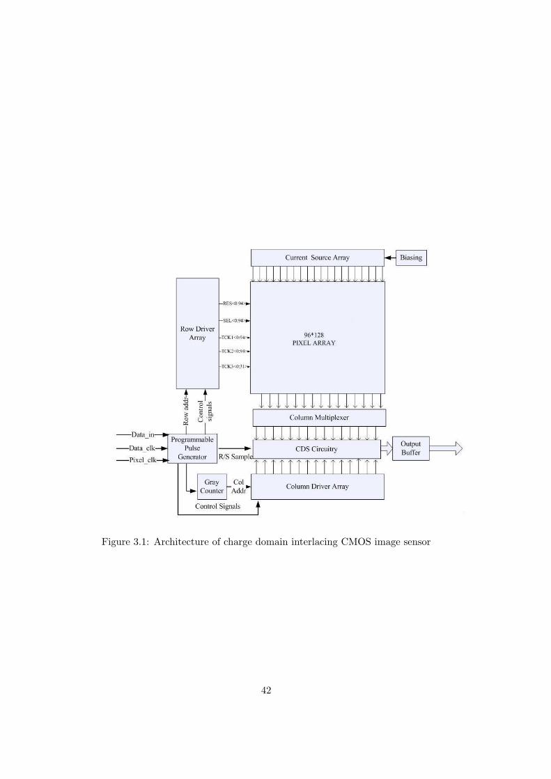
3.1 Architecture of the Charge Domain Interlac-ing Image Sensor
The figure 3.1 is the whole architecture of the sensor, which contains several
parts. I will introduced them as follow:
Pixel Array: the light sensitive part of the image sensor. It contain
96× 128 pixels, converting the light signal into a voltage signal.
Current Source Array: a current source is needed on every column bus.
The current source is used to bias the source follower in the pixel and charge
the parasitic capacitor of each column.
Column Multiplexer: according to the even or the odd field to select the
column bus processed by the column analog chain.
41
Figure 3.1: Architecture of charge domain interlacing CMOS image sensor
42
Column readout circuit: implementing the CDS (correlated double sam-
pling) and analog signal processing chain to readout the column bus and
output the processing signal.
Row Driver Array: decoding the gray code row address and providing
driving signals for the specific addressing pixel row.
Column Driver Array: when a specific row is addressed by the row driver
array(decoded from the row address), the column driver array will decode
the gray code to drive the column readout circuit column by column.
Programmer Pulse Generator: buffers the series input signals and use
different clock domain transfers from the series input signals to the parallel
control signals. These control signals contain the row addressing signals, the
pixel control signals, the column bus readout control signals and so on.
Gray Code Counter: when the counter is triggered, 7 bits gray address
code is produced with the rising edge of the CLK. This code will be used to
address and readout the column readout circuits.
Output buffer: the output stage of the sensor, buffers the analog output
signal to enhance the driving capability of the sensor output.
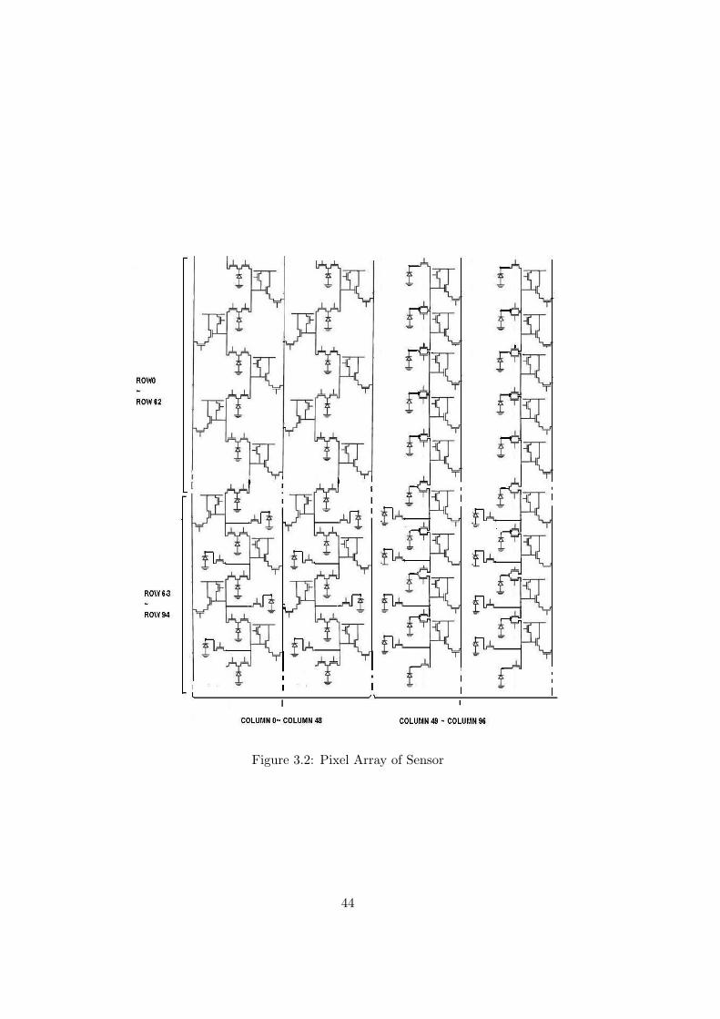
3.2 Pixel Array
3.2.1 Pixel Design
The pixel array contains two type of pixel designs which are introduced
in the chapter 2. And both two pixel designs can be organized into two
different readout directions. For figure 3.2, from row 0 to row 62, there is
the two photodiode shared amplifier structure pixel. From row 63 to row
94, there is the three photodiode shared amplifier structure pixel. From the
Column line 0 to Column line 48, these pixels use the mirror column readout
direction structure to readout.
As mentioned in last chapter and shown in figure 3.3, a basic cell of
43
Figure 3.2: Pixel Array of Sensor
44
Figure 3.3: Schematic of two different pixel designs
two shared photodiodes amplifier structure includes two photodiode parts
and two transfer gates(TG1 and TG2), a reset transistor(RST), a source
follower(SF), and a row selector(SEL). Because these two photodiodes can
have a shared readout, every photodiode is divided in two parts which have
the same shape and were placed in two basic cells. This project use the
pinned photodiode which is composed of a p+ implantation, n implantation
and p substrate. All of other transistors in this cell are NMOS transistor
which are placed in the p-well(ground). The control signals of this structure
are explained in the table 3.1 below :
Signal DescriptionVDDI pixel array power supply (3.3V)GND Analog GroundRST Reset signal, high and low voltage level can be adjustedSEL Row select signal, high voltage level can be adjusted,
low level is groundCOL Column busTG transfer gate, high and low voltage level can be adjusted
Table 3.1: 4T pixel signals description
45
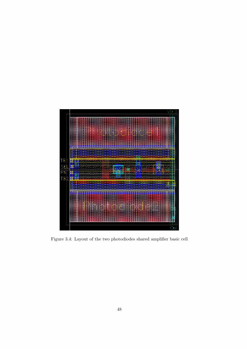
3.2.2 Layout Considerations
Figure 3.4 and Figure 3.5 are layouts of the basic cell of two photodiodes,
and three photodiodes shared amplifier structure respectively. The basic
cell of “two photodiodes shared amplifier structure” contains two photodiode
parts, but one is just the half of the actual photodiode size. The pitch of this
structure is 10um×10um. The fill factor of this pixel design is 46.37%. The
other type “three shared photodiodes amplifier” structure contains one more
photodiode and one more transfer gate. Because this three shared structure
is used in both even and odd field, and contains one independent photodiode
and 2 shared photodiodes, the area of this basic cell is 20um×10um. The fill
factor of this structure pixel is 47.8% which improves the fill factor compared
with two photodiode shared amplifier structure. As shown in figure 3.4, the
big red area is the pinned-photodiode part. Along every photodiode there
is a blue rectangular structure which is the transfer gate of the 4T pixel
structure. The readout structure is located in the middle of structure, which
makes two photodiodes having the same distance to the readout structure.
The three transistors in readout structure is reset transistor(RST), source
In this particular project, the pixel design should consider two aspects,
first of all, symmetric requirement. These pixels are used in charge domain
interlacing design. Some photodiodes will be shared by different readout
circuits and charges stored in the photodiode will be transferred in two dif-
ferent directions. Even for column 0 to column 48, the readout direction is
different in neighboring rows. Thus, the two photodiodes share one readout
circuit should be fully symmetric with respect to the readout structure of
the pixel. For the three photodiode shared amplifier structure(figure 3.5),
the photodiode 2 is just being readout by one readout circuit, and controlled
by one transfer gate. But the other two photodiodes 1 and 3 are shared in-
dividually by two readout structures in neighboring rows and controlled by
46
two transfer gates. In this situation, the layouts of the three photodiode
are hard to be exactly the same to each other. But if we just consider the
charge domain interlacing scan mode, the output signal is from the integra-
tion voltage of charges produced by photodiode 1 and 2 together, or charge
produced by photodiode 2 and 3 together. No matter which combination,
the photodiode 2 is always included. Considering the photodiode 1 and 2
together as a readout unit, photodiode 2 and 3 together as a readout unit,
these two units should be symmetric.
To control the transfer gate for photodiode2, there is a metal line con-
nected with TG3 of all the pixels in one particular row. In order to keep
the metal away from the photodiode, we just could connect this TG3 at one
end of the gate TG3. But for the symmetry of the layout and to avoid the
non-even electrical potential across the gate of TG3, a second metal TG3
should be added to balance the electrical potential in the poly of TG3.
Second, to reduce the kTC noise, the capacitance of the floating diffusion
should be small, specially for this project, the floating diffusion of two or
three photodiode connected together for one readout circuit, which will be
larger than normal design. In this situation, the layout should try to control
the area of the floating diffusion to reduce the kTC noise.
3.3 Current Source Array
3.3.1 Column Current Source Design
From the pixel operation, we know that a current source is necessary for each
column bus. The current column source Icol is not required continuously
during an imaging cycle, but only when the pixel values require to be reset
for integration and readout. On one hand, the column current source is
used to bias the source follower of pixel. On the other hand, for every pixel
connected in one column bus, the row select transistor introduces a parasitic
capacitor to the column bus, the column current source was used to charge
47
Figure 3.4: Layout of the two photodiodes shared amplifier basic cell
48
Figure 3.5: Layout of the three photodiodes shared amplifier basic cell
49
or discharge these capacitors to the stable value.
The figure 3.6 shows the circuit of one column current source. It can be
divided into two parts according to the function. The first part is the current
source (M5 and M9). Saturated PMOS transistor M9 and NMOS M5 is
operated as current sources. The source ends of two transistor are connected
together, which could improve the Power-Supply Rejection Ratio(PSRR) to
reduce the influence of the jitter from power and ground. A stable current
reference for current mirror can be provide by this structure. The second
part is the current mirror (M3 and M4). The same W/L ratio of M3 and M4
makes the current Id(M3) mirroring the Id(M4) which is equal to 12uA. The
last part M2 and M11 are used to allocate the current value for column bus.
When CS = 2.7V , the NMOS M2 is “on”, nearly the total output current
of M3 is concentrated to Icol(Id(M2)). When CS= 1.4V, the total current is
flow into the PMOS transistor M11, the NMOS M2 is turn “off”. When the
CS is adjusted in between, the column current can be changed between 0 to
12uA. Thus, based on this current source circuit, the current ratio of PMOS
and NMOS can be relocated easily, then the column current value can be
controlled by input bias. But combined with the control mechanism, in this
sensor, CS just can choose 2.7V or 1.4V by the digital control signal NSEL.
This limitation can be improved in the future design to give more choices
for column current.
VDDI pixel array power supply (3.3V)gnd Analog Ground
Biasn Bias voltage produce by Biasing Part(3.3V)Biasp Bias voltage produce by Biasing Part(855mV)
CS switch of the col current which is controlled by one ofthe input control signal(NSEL) of the sensor. When digital signalNSEL=“1”(1.8V), CS=2.7V; when NSEL=“0”(ground), CS=1.4V
COL Corresponding column bus
Table 3.2: Current source signal description
50
Figure 3.6: Schematic of column current sensor
3.3.2 Design Considerations
To design of the column current source is a tradeoff between the speed of
the pixels and the noise performance. From the speed consideration, the
large column current results in a the fast speed for charging and discharging
the parasitic capacitance. From the noise consideration, a large current
also means a large gm of the source follower, and means a large thermal
noise contribution to the output signal. So a compromise between these two
aspects is made for the column current.
The design of the column current source is critical because the trans-
fer gain of the in-pixel source follower is sensitive to this column current
source. Even the small variation on the current value would change the
source follower gain, which is one of origins of the non-linearity of the pixel.
This current source structure is repeated in every column, so the layout
of the current source in each column must fits the pixel pitch 10um.
51
Output buffer Bus_rst<n>
Out_en<n>
SHS
SHR
Cs
Cr
ReadS<n>
col<n>
ReadR<n>
RST
SEL
TG
VDD3v3
GND
Cload
Figure 3.7: Column signal processing chain
3.4 Column Readout Circuit
Since the pixel array design and the current source array design are intro-
duced in last two sections, we can get the signal and reset voltage from the
column bus. To implement the CDS technology and get the output signals
of the whole pixel array with good driving capability and correct timing
sequence, an signal processing chain is needed for every column bus. Figure
3.7 is the schematic of the whole signal processing chain for one column,
which shows the whole course from light input to the sensor analog output.
This signal processing chain can be divided into two parts, the sample and
hold(S/H), the readout timing control, and the output buffer.
3.4.1 Sample-hold and Readout Circuit
This part will describe how to sample and hold the output signals and read-
out for every column bus when a particular pixel row is addressed. As figure
3.7 shows, every column bus has two 1pf capacitors (Cs and Cr) which are
used to store the reset level and the signal level respectively. The timing
diagram of control signals of the column readout circuit is shown in figure
3.8.
1. When a row is addressed, all of the pixel output signals in that row
52
Line timeSEL
RST
TG
SHR
Line<n> Line <n+1>
SHS
ReadR<0>
col_rst<0>
ReadS<0>
Out_en<0>
ReadR<1>
col_rst<1>
ReadS<1>
Out_en<1>
Figure 3.8: Timing diagram of 4T pixel and CDS readout
53
should be sampled and stored in Cs or Cr at the same time. Thus,
the sample signal SHS and SHR are global signals for all the column
readouts. When the row select signal SEL is high, that row is ad-
dressed. Then after the reset, the reset levels of all pixels in that row
are sampled and stored in corresponding column Cr by SHR = 1; af-
ter charges which are accumulated in the photodiode were transferred
to the floating diffusion(TG = 1), the signal levels of all pixels are
sampled and stored in the corresponding Cs by SHS = 1. Until now,
signals of all columns are stored in their corresponding capacitor.
2. After sample and hold the signal in capacitors Cr and Cs, readout
circuits will be driving one by one from column 0 to column 96 and
finished one row readout in one line time. For instance, when driv-
ing column readout circuit of column〈0〉, switches of ReadR〈0〉 and
output enable(out en) will open to transfer the stored reset signal to
the output bus. Then the bus was reset by col rst〈0〉 = 1. After the
reset(col rst〈0〉 = 0), the video signal stored in the Cs〈0〉 will be trans-
ferred to output bus (ReadS〈0〉 = 1&out en〈0〉 = 1). When both reset
signal and video signal were readout, the output bus will reset again
by col rst〈0〉 = 1. Finished the readout of column line 0, the column
line 1, 2,... will be readout at the same principle until the last column
line 96. It is important to notice that the necessary subtraction of the
two signals to complete the CDS action is done off-chip.
3. Then the next row is addressed, the readout process depicted in 1 and
2 will be repeated again until the whole pixel array was scanned.
These readout control signals are listed in the table 3.3 below.
For this particular application, some columns (from column line 0 to
column line 48) have different readout directions for odd and even fields.
For example column line 〈1〉 is not only connected the odd field output of
the first column, but is also connected with the even field output of the
54
field_en
col<0> col<1> col<2> col<47> col<48>
Column readout circuit <0>
Column readout circuit <1>
Column readout circuit <2>
Column readout circuit <n>
Column readout circuit <47>
Figure 3.9: Principle of column multiplexer
Signal Type Sensitivity DescriptionSHS input active high Global sample signal for the Signal level.
High is 3.3V, low is groundSHR input active high Global sample signal for Reset level.
High is 3.3V, low is groundReadR〈n〉 input active high Readout switch for the reset signal
from Cr of the column. High is 3.3V , low is groundReadS〈n〉 input active high Readout switch for the video
signal from Cs of the column. High is 3.3V, low is groundcol rst〈n〉 input active high Reset pulse for the column readout bus.
If col rst = 1, then the readout bus was reset.High is 1.8V, low is ground
out en〈n〉 input active low Output enable signal, when reset signalor video signal were readout in column n, then
out en〈n〉 = “0′′. High is 3.3V, low is analog groundfield en input level field en = 1 means odd field scan,
and field en = 1 means even field scan
Table 3.3: Column Readout Control Signals
55
second column. Then, to process these readout signal, the column bus will
be selected by different column signal processing chains. In figure 3.9 we
can see the field en signal to select a field. When the scan field is the odd
field(field en = 1), the output direction of these pixels is the right, the 2
to 1 multiplexer will choose the column line 〈1〉 for column readout circuit
〈0〉, column line 〈2〉 for column readout circuit 〈1〉... When the scan field
is the even field(field en = 0), the output direction changes to the left.
The 2 to 1 multiplexer will choose the column line 〈0〉 to be processed by
column readout circuit〈0〉, choose column line 〈1〉 to be processed by readout
circuit〈1〉, and so on.
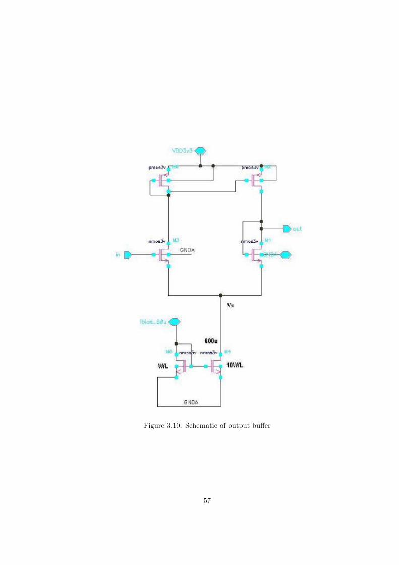
3.4.2 Output Buffer
The output stage of the sensor should satisfy a number of special require-
ments. One of the most important is to minimize the output impedance
so that the output voltage will not be affected by the load impedance. An
analog buffer which has a low output resistance, high driving capability can
satisfy the requirement. Another requirement for the output stage in this
sensor is the wide dynamic range. In this project, a CMOS buffer with a
wide dynamic range and a capacitive load driving capability is needed. This
buffer is connected to the output of all 96 column readout circuits which
can buffer and delivery the reset signal and video signal of column 1 to col-
umn 96 in turn. This amplifier will use a differential pair with an active
current mirror structure and implement as a unity gain feedback topology.
In figure 3.10, the M0 and M2 are identical, M3,M1 are identical too. The
input range of output buffer should tolerate the reset signal and the min-
imum video signal. The minimum input voltage for this buffer is equal to
VDS4 + VGS3,min, and the maximum allowable input voltage will put input
transistor M3 at the edge of the triode region which is
56
Figure 3.10: Schematic of output buffer
57
Vin − Vth = VG3 = V DD3v3− |VGS3|
Vin,max = V DD3v3− |VGS3|+ Vth
(3.1)
Suppose Vth is about 0.7V in this technology, and the overdriver VGS −
Vth = 0.3V . Then Vin,max = 3.3−1+0.7 = 3V , and Vin,min = 0.3+0.3+0.7 =
1.3V . From the simulation of the analog chain, we can know the reset voltage
is around 2.7V. And the maximum pixel voltage swing was estimated to be
1V. Then the minimum video signal we get is about 2.7− 1 = 1.7V , which
is higher than the minimum voltage of the buffer. So this buffer design is
enough for this application.
Another concern about the buffer is the settling time. From transient
simulation we can see the step response of the amplifier in figure 3.11. And
if we define the error less than -50dB (0.3% accuracy), then the settling
time is 81.3ns. In this project, the pixel clock for one column readout is
416kHz, and sample frequency of off chip ADC is about 800kHz, which is
about the two times of the pixel clock. This settling time could satisfy the
requirements of this application. From the AC response of the close loop
amplifier 3.12, we can see the united gain bandwidth is about 10MHz, which
is far beyond the requirement of the output stage.
Figure 3.11: Buffer settling time with the accuracy
58
Figure 3.12: Close loop AC response of buffer
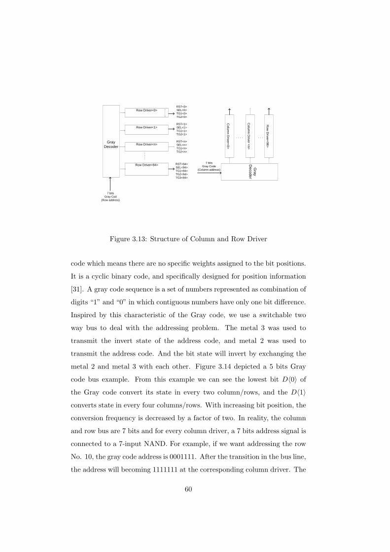
3.5 Row and Column Driver
In this part, the row and column driver design will be introduced. There
are two basic functions for the row driver and column driver. One is the
addressing and decoder. The other one is according the decoding signal
to produce driving signals for the target row or column. The structure of
the column and row driver are shown in figure 3.13. These row and column
drivers are basically digital circuits. Normally, they can be easily designed in
hardware description language and automatically generated by CAD tools.
In the image sensor design, the row and column driver should fit the pixel
pitch which is 10um for the column and row driver(some of the row drivers
should fit the 20um due to the three photodiode shared amplifier structure).
No software tools can do the layout fitting to the pixel pitch. Then the
column and row driver should be designed and layout at gate level.
3.5.1 Gray Code Addressing
In this project, we use a Gray code as the address signal to addressing
the column or row. The Gray Code is unweighed and is not an arithmetic
59
Row Driver<0>
Row Driver<1>
Gray Decoder
Row Driver<94>
Row Driver<n>
7 bIts Gray Cod
(Row address)
RST<1>SEL<1>TG1<1>TG2<1>
RST<0>SEL<0>TG1<0>TG2<0>
RST<n>SEL<n>TG1<n>TG2<n>
RST<94>SEL<94>TG1<94>TG2<94>TG3<94>
Row
Driver<96>
Gray
Decoder
Colum
n Driver<0>
Colum
n Driver <n>
7 bIts Gray Code
(Column address)
Figure 3.13: Structure of Column and Row Driver
code which means there are no specific weights assigned to the bit positions.
It is a cyclic binary code, and specifically designed for position information
[31]. A gray code sequence is a set of numbers represented as combination of
digits “1” and “0” in which contiguous numbers have only one bit difference.
Inspired by this characteristic of the Gray code, we use a switchable two
way bus to deal with the addressing problem. The metal 3 was used to
transmit the invert state of the address code, and metal 2 was used to
transmit the address code. And the bit state will invert by exchanging the
metal 2 and metal 3 with each other. Figure 3.14 depicted a 5 bits Gray
code bus example. From this example we can see the lowest bit D〈0〉 of
the Gray code convert its state in every two column/rows, and the D〈1〉
converts state in every four columns/rows. With increasing bit position, the
conversion frequency is decreased by a factor of two. In reality, the column
and row bus are 7 bits and for every column driver, a 7 bits address signal is
connected to a 7-input NAND. For example, if we want addressing the row
No. 10, the gray code address is 0001111. After the transition in the bus line,
the address will becoming 1111111 at the corresponding column driver. The
60
NAND in the addressed row driver will output a falling edge as the decode
signal . The other NAND for non-addressed columns drivers will still be
“1”. When the load row address is 1111111, then without any transition in
this switchable address bus, the row 128 was addressed. The decoder part
D<0>
D<1>
D<2>
D<3>
D<4>
Figure 3.14: 5 bits gray code bus
in both row and column driver are the same Gray code addressing bus with
7-input NAND corresponding to every column/row. But for row addressing,
the row address signal is produced by FPGA on the PCB, then the driving
sequence for the row is flexible. For column addressing, the column address
is produced by a Gray code counter in the sensor. This gray counter can be
reset by the input control signal. If the reset signal is not active, the counter
will keep counting to produce the column address in turn.
3.5.2 Row and Column Driver Array
A row driver is necessary for every pixel row. For a 4T pixel, signal like
“RST 〈n〉”, “TGs〈n〉” and “SEL〈n〉” are generated by row driver 〈n〉 ac-
cording to the decode signal. The figure 3.15 above is the schematic of the
row driver. When address present in 7-input NAND is 1111111, then this
row is addressed. The following table 3.4 describes the input signal behav-
61
SELn
RSTn
TG1n
TG1Gn
Voltageshift
Voltageshift
Voltageshift
Voltageshift
SEL<n><0><1><2><3><4><5><6>
TG1<n>
TG2<n>
RES<n> TG2Gn
Vresel_H GNDA
TG_H TG_L
TG_H TG_L
Vresel_H Vresel_L
Figure 3.15: Schematic of Row Driver
Signal Type Sensitivity DescriptionSELn input active low The row select pulse, which can produce a row select
signal for the selected 4T pixel row, the signalcomes from the programmable pulse generator.
RSTn input active low The reset pulse, which can produce RST signalfor the selected 4T pixel row, this signal comes
from the programmable pulse generator.TG1n input active low The transfer gate pulse which will produce
TG1 signal for the selected pixel row.TG2n input active low This is the transfer gate pulse
which will produce TG2 signal for the selected pixel row.TG1Gn input active low This is the global signal for the transfer gate pulse
produced by programmable pulse generator. When thissignal is active, then TG1 of all rows will be open.
TG2Gn input active low This is the global signal for the transfer gate pulseproduced by programmable pulse generator. When this
signal is active, then TG2 of all rows will be open.Vresel H input n.a High voltage for pixel reset (RST)
and row select (SEL) signal.Vresel L input n.a Low voltage for reset signal (RST)TG H input n.a High voltage for transfer gate (TG1/TG2)TG L input n.a Low voltage for transfer gate (TG1/TG2)
Table 3.4: Row driver input signals
62
Signal Type Sensitivity DescriptionReadRn i input active low A programmable readout pulse that is
going to generate a reset signal readoutsignal for selected column readout
ReadSn i input active low A programmable readout pulse thatis going to generate a video signal
readout for selected column readoutEn out i input active high A programmable readout pulse
that is going to generate enablereadout for selected column readout
resetn i input active low A programable readout pulse that isgoing to generate col rst (table 3.3)
for selected column readout
Table 3.5: Column Driver input signals
ior of the row driver, and the output signals of the row driver were already
introduced in table 3.1.
These input signal are digital pulses which has the 1.8V as the high level,
0V for the low level. In order to driving transistors in the analog circuit, a
voltage shift from 1.8V to power supply for every output driving signal is
needed. The power supply for every driving signal is independent and can
be adjusted around 3.3V.
The Column Driver has a similar structure as the row driver, and all
the column driver output signals (ReadS, ReadR, out en, and col rst ) have
been introduced in table 3.3. Table 3.5 introduce the input signals of the
column driver. These signals are digital pulses (high = 1.8V ) which are
generated from programmable pulse generator.
3.6 Programmable Pulse Generator
The programmable pulse generator is a purely digital circuit which buffers
the series input data and uses different clock domain transfer from the series
input signals to the parallel control signals. These control signals contain
the row addressing signals, the pixel control signals, the column bus readout
63
control signals and so on.
First, DATA CLK is 24 times of the frequency of the pixel clock(CLK).
Then DATA CLK can shift 11 bits valid DATA IN in the last 11 DATA CLK
pulses of one pixel CLK cycle. In one pixel CLK can write one 7 bit register.
These are eight different 7 bit registers to generate the different control
signals. In this 11 bits data, the first 4 bits are the address for addressing
the target register. The next 7 bits represent the data we want to write into
the register. The timing diagrams of the DATA IN, CLK, and DATA CLK
are shown in the figure 3.16. DATA IN is the only control signal input
pad for the sensor. DATA CLK is the data clock to write into the register.
CLK is the main clock for the pixel readout. At the rising edge of the
DATA CLK, the DATA IN were shifted into the register, because of the
limited depth of the input register, only during the last 11 cycles, DATA IN
will be written into the register. In this example, a bitstream “01111000000”
was shifted into sensor. Then we can know the first 4 bits are referring to
the address“1110”, then reg11〈6 : 0〉 was write into “0000001”. The detailed
allocation of the register will be explained in table 3.6.
Figure 3.16: Timing Diagram of Sensor Input
The programmable value of Reg1 was related to the timing of setting the
ReadR signal. The programmable value of Reg4 was related to the timing
of resetting the ReadR signal. And the programmable value of Reg7 was
related to the timing of resetting the ReadS signal. Reg 11 was related to
set the ReadS signal. Out en and col rst are also related to these timing
sequence.
64
For 7 bit register 11 − 13, nearly every bit in these registers are con-
nected with the corresponding control signal. In this way, through program
different value to register 11− 13, we can change states of these control sig-
nal to produce the right timing for sensor work. The table 3.7 listed detail
information about these registers.
Register Address contentReg1 0001 SR resetReg4 0110 SR setReg7 0100 SS resetReg10 1111 SS setReg11 1110 pulse registerReg12 1010 pulse registerReg13 1011 pulse registerReg14 1001 row address
Table 3.6: Register Allocation
Register Connected signal DescriptionReg11〈0〉 resetoff If resetoff = 1, then col rst signal for
the column readout reset is not active anymore.Reg11〈5〉 NSEL If NSEL = 1, then current source switch onReg11〈6〉 SSHn If SSHn = 0, then column address gray code
counter is reset to 0Reg12〈0〉 SELLALLn If SELLALLn = 0, all rows are addressed togetherReg12〈1〉 SHRReg12〈2〉 SHSReg12〈3〉 odd sel If field en = 1, then means odd field scan,
otherwise means the even field scanReg12〈6 : 4〉 TG3Gn
TG2Gn, and TG1GnReg13〈4 : 2〉 TG1n,
TG2n, and TG3nReg13〈5〉 ROWnReg13〈6〉 RESn
Table 3.7: Pulse Generation Registers
65
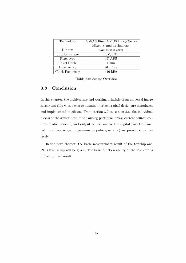
3.7 Sensor Overview
Figure 3.17 is the final layout of the image sensor. And the table 3.8 conclude
some basic specifications of the sensor.
Figure 3.17: Layout of the Whole Image Sensor
66
Technology TSMC 0.18um CMOS Image SensorMixed Signal Technology
Die size 2.3mm× 2.7mmSupply voltage 1.8V/3.3V
Pixel type 4T APSPixel Pitch 10umPixel Array 96× 128
Clock Frequency 416 kHz
Table 3.8: Sensor Overview
3.8 Conclusion
In this chapter, the architecture and working principle of an universal image
sensor test chip with a charge domain interlacing pixel design are introduced
and implemented in silicon. From section 3.2 to section 3.6, the individual
blocks of the sensor both of the analog part(pixel array, current source, col-
umn readout circuit, and output buffer) and of the digital part (row and
column driver arrays, programmable pulse generator) are presented respec-
tively.
In the next chapter, the basic measurement result of the testchip and
PCB level setup will be given. The basic function ability of the test chip is
proved by test result.
67
68
Chapter 4
Initial Measurement Results
This chapter focus on the measurements of the designed sensor. The mea-
surement set-up will firstly be described, then the most important part, the
initial measurement results, will be presented, as well as the analysis and
discussion of the results.
4.1 Measurement Setup
The setup of the measurement can be found in Fig 4.1, where the under-
test image sensor is placed on the designed printed circuit board(PCB). The
PCB is connected to the computer to process the digital image signal. On
the oscilloscope we can also see the waveform of the sensor analog output.
It can directly help us to know whether sensor is working normally. To
better understand the measurement setup, the IO pins of designed chip are
described in table 4.1.
The measurement PCB is mainly composed by under-test sensor, FPGA,
ADC, frame grabber, quarts crystal, and power supply system. The FPGA is
the central control part of the PCB. First of all, it generates the suitable pixel
clock, data clock, and data-in for the image sensor. Changing the driving
sequence and working mode of the sensor will be very flexible by changing
the programmable input data sequence. Secondly, the FPGA supplies the
69
Under Test Image Sensor
Power Supply
+6 -6
ADC
FPGA
Analog output
GND
OscilloscopeFrame
Grabber
PC
lightDigital Signal
Processing&
Display
Programmer
Figure 4.1: Measurement setup for the sensor
Pin name Type DescriptionDATA CLK Input clock Clock for writing series data into register(10MHz)DATA IN Digital input Programmable data input of sensor
CLK Input clock pixel clock, in one clock period,one pixel was readout(416.6kHz)
Aout analog output the analog output include the reset and video signalVDD3V3 power supply main power for analog circuit(3.3V)GNDA ground analog groundVDDI power supply adjusted pixel array voltage(3.3V)TG L power supply adjusted low voltage for transfer gate (0V)TG H power supply adjusted high voltage for transfer gate(3.3V)
Vresel H power supply adjusted high voltage of Vg(3.3V )for pixel reset and row select transistor
Vresel L power supply adjusted low voltage of Vg
for pixel reset transistor(0V)VSS ground digital groundVDD power supply main power for digital circuit (1.8V)
Test pads test output reserving 5 test pads for important biasingsignals, middle stage output signal and so on
Table 4.1: IO pins of the designed image sensor
70
Figure 4.2: ADC supply clock
sample clock, digital input data for off-chip ADC, which can control the
working status of ADC, to make the ADC sample the output analog signal
of sensor and convert them to 12 bits digital number. Finally, the FPGA is
also connected with the frame grabber to provide the clock and other control
signals for the grabber.
In this measurement setup, we choose an 12 bit, 40MHz A/D converter
to process the analog output of the sensor. To suit the common mode input
voltage range and 1V p-p input range of the ADC, a resistant divider is used
to adjust the sensor output signal to the half of the original signal. Luckily,
there is a variable gain amplifier in the ADC, which can compensate for the
lost of the signal input range and achieve 2-V full scale range. Of course, in
this transition, the noise performance will also be affected.
In the figure 4.2, the timing relationship between the sensor pixel clock,
and ADC sample clock is shown. In one sensor clock period, there are
two ADC sample periods, which sample the reference reset level and the
video signal level respectively. The allows for Correlated-Double Sampling
afterwards. Clk FG is the clock of the frame grabber which has some delay
with CLK ADC
4.2 Measurement Result
4.2.1 Sensor Analog Output
The sensor can output an analog signal and it clearly show light response.
The integration time is 17.4ms.
71
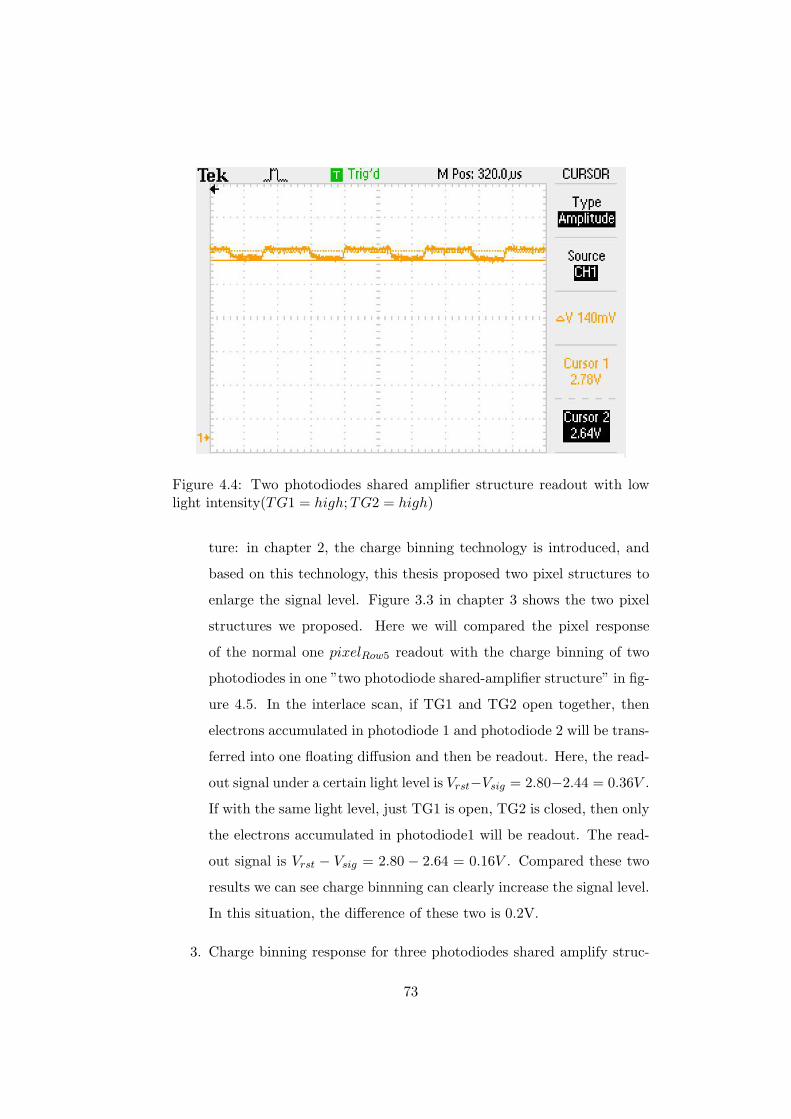
Figure 4.3: Two photodiodes shared amplifier structure readout with stronglight intensity(TG1 = high;TG2 = high)
1. Basic light response: to measure the image senor, the basic thing is to
test the light response of the sensor. The pixels in the fifth row are
readout as example. Figure 4.3 and figure 4.4 are “two photodiodes
shared-amplifier structure” output under strong light condition and
low light condition in respectively. The two transfer gates TG1〈5〉,
and TG2〈5〉 which are connected to the two photodiode are opened
together. Because we did not complete CDS technology fully on chip,
here we can see the both the reset level and the video signal level.
Cursor1 indicates the pixel reset level, and cursor2 indicates the pixel
signal level.
From the figure 4.3 we can see Vrst = 2.78V , Vsig = 1.16V . After
substraction, the real signal across these two photodiodes is Vrst −
Vsig = 1.62V (nearly saturated). In figure 4.4 we can see Vrst = 2.78V ,
Vsig = 2.64V . The real signal in this low light situation is Vrst−Vsig =
0.14V . From the figure above we can clearly see the light response.
2. Charge binning response for two photodiodes shared-amplifier struc-
72
Figure 4.4: Two photodiodes shared amplifier structure readout with lowlight intensity(TG1 = high;TG2 = high)
ture: in chapter 2, the charge binning technology is introduced, and
based on this technology, this thesis proposed two pixel structures to
enlarge the signal level. Figure 3.3 in chapter 3 shows the two pixel
structures we proposed. Here we will compared the pixel response
of the normal one pixelRow5 readout with the charge binning of two
photodiodes in one ”two photodiode shared-amplifier structure” in fig-
ure 4.5. In the interlace scan, if TG1 and TG2 open together, then
electrons accumulated in photodiode 1 and photodiode 2 will be trans-
ferred into one floating diffusion and then be readout. Here, the read-
out signal under a certain light level is Vrst−Vsig = 2.80−2.44 = 0.36V .
If with the same light level, just TG1 is open, TG2 is closed, then only
the electrons accumulated in photodiode1 will be readout. The read-
out signal is Vrst − Vsig = 2.80 − 2.64 = 0.16V . Compared these two
results we can see charge binnning can clearly increase the signal level.
In this situation, the difference of these two is 0.2V.
3. Charge binning response for three photodiodes shared amplify struc-
73
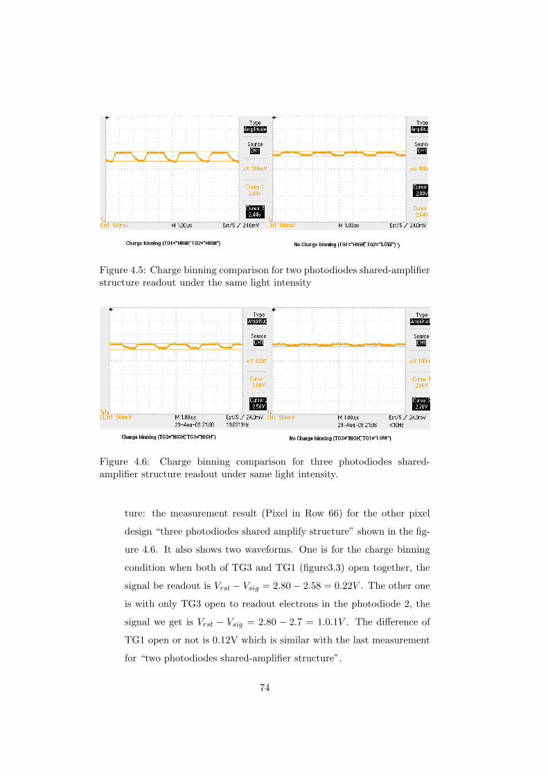
Figure 4.5: Charge binning comparison for two photodiodes shared-amplifierstructure readout under the same light intensity
Figure 4.6: Charge binning comparison for three photodiodes shared-amplifier structure readout under same light intensity.
ture: the measurement result (Pixel in Row 66) for the other pixel
design “three photodiodes shared amplify structure” shown in the fig-
ure 4.6. It also shows two waveforms. One is for the charge binning
condition when both of TG3 and TG1 (figure3.3) open together, the
signal be readout is Vrst − Vsig = 2.80− 2.58 = 0.22V . The other one
is with only TG3 open to readout electrons in the photodiode 2, the
signal we get is Vrst − Vsig = 2.80 − 2.7 = 1.0.1V . The difference of
TG1 open or not is 0.12V which is similar with the last measurement
for “two photodiodes shared-amplifier structure”.
74
It should be clear that the light conditions for these two pixel structure
measurements is different. So it can not compared these two pixel structures
from data above.
4.2.2 image result
In this subsection, the image result we get will be shown here. The figure
4.7 is image we get from the progressive scan.Because of the rotation of
the figure, the top part is the three photodiodes shared amplifier structure.
The bottom part of the image uses the two photodiodes shared amplifier
structure.
The figure 4.8 is the mickeymouse image get from the interlace scan
in the field integration mode. The top one is the even field scan, and the
bottom one is the odd field scan.
Compared these two figures, we can see the signal level in the background
of figure 4.8 is clearly has more light than figure 4.7. But in reality, these
image are get from the same illumination condition. This reveals that the
charge domain interlacing principle can enhance the signal level in certain
degree.
4.3 Conclusion
With the very first measurement results of the designed sensor, it has been
shown that sensor is working and the proposed pixel structures can truly
enhance the signal level to a certain degree. The detailed performance mea-
surement and analysis will be done in the future.
75
Figure 4.7: Image result of progressive scan
76
Figure 4.8: Image result of interlace scan
77
78
Chapter 5
Conclusion and Future Work
5.1 Conclusion
CMOS image sensors suffer from several noise sources which will affect the
image performance especially under low illumination. To improve the overall
quality of the image, a high S/N ratio and wide dynamic range are desired.
To improve the S/N ratio, a lot of work has been done to reduce many
kinds of noise sources. It can be done by using correlated double sampling
technology to cancel the reset noise and the transistor offset and so on.
Reducing the noise also can be done by improve the technology and the
device to reduce the noise sources at their origins. But improving the S/N
ratio can also be achieved by enhancing the signal level under the same light
condition.
Inspired by the field integration mode of the interlaced scan, we can
add the signal of neighboring rows signal together and using the interlace
mode to achieve a the high signal level under the same light conditions. To
realize this mechanism, the easiest way is to add the pixel readout signal in
voltage domain or even in the digital domain. But for an image sensor a
lot of noise sources are coming from the readout course of the pixel. If the
readout signal is added in the voltage domain, this will increase the noise
level of the output stage which can not achieve the purpose of improving
79
the S/N ratio. To deal with this problem, this thesis proposes two different
pixel structures based on 4T APS structure and both of them can combine
the collected charges of two pixels and then readout them together.
The first pixel structure uses one pixel readout structure connected to
two photodiodes, by using one floating diffusion to combine the photon-
generated electrons from two pixels together and then readout this com-
bined signal. From the photodiode standpoint, each photodiode is connected
with two readout structures and two transfer gates which are active in the
even field scan and odd field scan respectively. The other pixel design uses
one pixel readout structure connected to three photodiodes. Both of these
structures can realize the charge domain interlacing principle to enhance the
signal level from the front end of the sensor.
To test these pixel designs and the working principle, a programmable
universal image sensor driving circuit architecture was proposed, which can
driving and readout the pixel array flexible and easily change it through
different programming. This sensor can not only support progressive scan,
frame integration interlace scan mode,voltage domain field integration inter-
lace scan mode, but also can realize the charge domain interlacing principle
with some special pixel designs.
The designed image sensor is implemented in TSMC 0.18um process,
and the first measurement result were given. Further testing results are
expected after September 2009.
5.2 Future Work
Due to the limited time, only preliminary measurement results are included
in this thesis, more measurements will be performed later in order to give
further details about the performance analysis especially with respect to
the noise aspects. On the other hands, better understanding the principle
is important as well. More measurement need to be done to compared
80
the different pixel designs with respect their noise performance and other
aspects. It is interesting to use the different scan modes and their analysis
to look for similarities and differences between the measurement results and
theoretical model.
81
82
Bibliography
[1] S.Morrison. A new type of photosensitive junction device. Solid-State
Electronics, 6,issue 5:485–494, 1963.
[2] J.Horton et al. The scanistor-a solid-state image scanner. Proceeding
of IEEE, 52:1513–1528, 1964.
[3] M.A.Schuster et al. A monolithic mosaic of photon sensors for solid
state imaging applications. IEEE Transactions on Electron Devices,
ED-13:907–912, 1966.
[4] G.P.Weckler. Operation of p-n junction photodetectors in a photon flux
integration mode. IEEE Journal of Solid-State Circuits, SC-2, 1967.