1 Charge Transfer between Isomer Domains on n + -Doped Si(111)-2×1: Energetic Stabilization R. M. Feenstra Dept. Physics, Carnegie Mellon University, Pittsburgh, Pennsylvania 15213, USA G. Bussetti, B. Bonanni, A. Violante, C. Goletti, P. Chiaradia Dipartimento di Fisica, NAST and CNISM, Università di Roma "Tor Vergata", Roma, Italy M. G. Betti, C. Mariani Dipartimento di Fisica and CNISM, Università di Roma "La Sapienza", Roma, Italy Abstract Domains of different surface reconstruction – negatively- or positively-buckled isomers – have been previously observed on highly n-doped Si(111)-2×1 surfaces by angle-resolved ultraviolet photoemission spectroscopy and scanning tunneling microscopy/spectroscopy. At low temperature, separate domains of the two isomer types are apparent in the data. It was argued in the prior work that the negative isomers have lower energy of their empty surface states than the positive isomers, providing a driving force for the formation of the negative isomers. In this work we show that the relative abundance of these two isomers shows considerable variation from sample to sample, and it is argued that the size of isomer domains is likely related to this variation. A model is introduced in which the electrostatic effects of charge transfer between the domains is computed, yielding total energy differences between the two types of isomers. It is found that transfer of electrons from domains of positive isomers to negative ones leads to an energetic stabilization of the negative isomers. The model predicts a dependence of the isomer populations on doping that is in agreement with most experimental results. Furthermore, it accounts, at least qualitatively, for the marked lineshape variation from sample to sample observed in photoemission spectra. I. Introduction The Si(111)-2×1 surface has been the subject of extensive study for more than 50 years. This reconstruction forms when Si is cleaved along a (111) plane, in vacuum. A bulk- terminated structure of the surface consists of a hexagonal arrangement of second- nearest-neighbor surface dangling bonds. For the reconstructed surface, early studies suggested a structural model consisting of alternating rows of raised or lowered dangling rows, with charge transferred between the lowered and raised rows hence forming the 2× periodicity on the surface [1]. However, in 1981 Pandey suggested a much different model, in which the surface rearranges such that the dangling bonds are nearest neighbors [2], as pictured in Fig. 1(a). Overlap between the dangling bonds of these rows of atoms (π-bonded chains) leads to energy lowering of the system. Optical properties of this surface have been the subject of considerable study over the past decades [3].
Transcript
1
Charge Transfer between Isomer Domains on n+-Doped Si(111)-2×1: Energetic Stabilization R. M. Feenstra Dept. Physics, Carnegie Mellon University, Pittsburgh, Pennsylvania 15213, USA G. Bussetti, B. Bonanni, A. Violante, C. Goletti, P. Chiaradia Dipartimento di Fisica, NAST and CNISM, Università di Roma "Tor Vergata", Roma, Italy M. G. Betti, C. Mariani Dipartimento di Fisica and CNISM, Università di Roma "La Sapienza", Roma, Italy Abstract Domains of different surface reconstruction – negatively- or positively-buckled isomers – have been previously observed on highly n-doped Si(111)-2×1 surfaces by angle-resolved ultraviolet photoemission spectroscopy and scanning tunneling microscopy/spectroscopy. At low temperature, separate domains of the two isomer types are apparent in the data. It was argued in the prior work that the negative isomers have lower energy of their empty surface states than the positive isomers, providing a driving force for the formation of the negative isomers. In this work we show that the relative abundance of these two isomers shows considerable variation from sample to sample, and it is argued that the size of isomer domains is likely related to this variation. A model is introduced in which the electrostatic effects of charge transfer between the domains is computed, yielding total energy differences between the two types of isomers. It is found that transfer of electrons from domains of positive isomers to negative ones leads to an energetic stabilization of the negative isomers. The model predicts a dependence of the isomer populations on doping that is in agreement with most experimental results. Furthermore, it accounts, at least qualitatively, for the marked lineshape variation from sample to sample observed in photoemission spectra. I. Introduction The Si(111)-2×1 surface has been the subject of extensive study for more than 50 years. This reconstruction forms when Si is cleaved along a (111) plane, in vacuum. A bulk-terminated structure of the surface consists of a hexagonal arrangement of second-nearest-neighbor surface dangling bonds. For the reconstructed surface, early studies suggested a structural model consisting of alternating rows of raised or lowered dangling rows, with charge transferred between the lowered and raised rows hence forming the 2× periodicity on the surface [1]. However, in 1981 Pandey suggested a much different model, in which the surface rearranges such that the dangling bonds are nearest neighbors [2], as pictured in Fig. 1(a). Overlap between the dangling bonds of these rows of atoms (π-bonded chains) leads to energy lowering of the system. Optical properties of this surface have been the subject of considerable study over the past decades [3].
randy
Text Box
Published in J. Phys.: Condens. Matter 24, 354009 (2012).
2
Some tilt, also known as buckling, can occur in the bonds that connect the surface atoms of the 2×1 π-bonded chain structure. Early theoretical studies were not able to determine the magnitude or the sign of this buckling since the relevant energetics require very high precision in the computations. More recent results indicated that the Si(111)-2×1 surface buckles in a positive sense whereas the Ge(111)-2×1 surface buckles in a negative sense [4], with the convention for the sign of the buckling defined in Fig. 1(a). Most recently, studies at low temperature have revealed new results for the buckling of Si(111)-2×1 surfaces of highly n-doped material [5]: With a combination of angle-resolved ultraviolet photoemission spectroscopy (ARUPS), scanning tunneling microscopy (STM), scanning tunneling spectroscopy (STS), and first-principles theoretical computations, it was found that both positive and negative buckling occurs on the surface. We refer to these two structures as isomers. It is observed that domains form on the surface in which all of the π-bonded chains are of one isomer type or the other. As a function of increasing temperature, ARUPS shows that the surface coverage of negative isomers decreases, so that at room temperature most of the surface is covered by positive isomers. It was revealed by STS that the edge of the empty surface state band for the negative isomers is lower than for the positive isomers, as indicated in Fig. 1(b) by SS
CEΔ , so that electron occupation of this band (i.e. for n-type material) provides a driving force for the formation of the negative isomers [5]. In the present work we present additional ARUPS data for the Si(111)-2×1 surface revealing considerable variation from sample to sample of spectral features related to negative and positive isomer domains. We argue that variation in the amount of charge transfer between the positive and negative domains, due to the effects of domain boundaries, provides a likely source for this variation. A method is developed for computing the total energy associated with charge transfer from the bulk semiconductor to the isomer domains at the surface, and also between surface domains of positive and negative isomers. For sufficiently small domains, it is found to be energetically favorable to transfer electrons from the surface states of the positive isomer domains over to negative isomer domains (i.e. because of the lower surface state energies of the latter). This phenomenon provides an explanation for the co-existence of domains of positive and negative isomers on the surface, thereby accounting for most of the existing experimental observations. Figure 2(a) shows a schematic phase diagram summarizing the existing experimental results for the relative abundance of the isomer types. Many experiments at doping concentrations of about 1×1018 cm-3 or lower reveal only positive (P) isomers, and those works are not explicitly referenced on the diagram. Our recent results of Ref. [5], using both ARUPS and STM/S, reveal mixtures of positive and negative isomers (P+N); the ARUPS study was performed on samples with doping concentrations of 4×10¹⁸ and 8×1018 cm-3, both at 100 and 300 K. A mixture of positive and negative isomers was observed in all cases. The STM/S work of Ref. [5] was done with material having doping
3
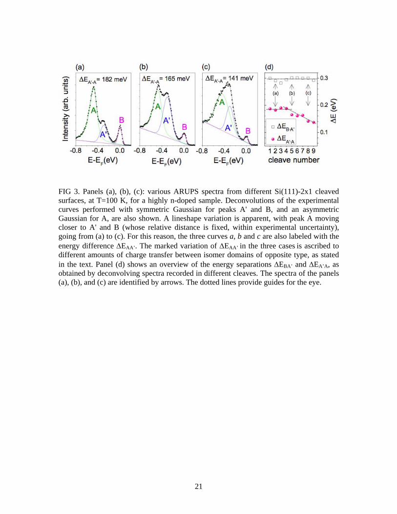
concentration of 2×1019 cm-3, at 8 K.1 The same material was also employed in the STM/S study of Ref. [6], at room temperature. Only positive domains were observed in that study, as indicated in Fig. 2(a), which appears to be contradictory to the ARUPS results of Ref. [5]; we return to this point in Section IV below. Also shown in Fig. 2(a) is the result from the STM/S work of Garleff et al. [7], that revealed only positive isomers at 8 K, using material with doping concentration of 6×1018 cm-3. Again, that result appears to be somewhat contradictory to the ARUPS results of Ref. [5], and this point is also addressed in Section IV. It should be noted that no data on the isomer abundance presently exists for material with doping concentration above 2×1019 cm-3, so we do not know whether such a surface would consist entirely of negative isomers or whether it would still be a mixture of isomer types. As already described above, it was proposed in Ref. [5] that a lower energy for the empty surface-state band of the negative isomers could provide a driving force for their formation. In terms of a phase diagram, this mechanism would be expected to produce purely negative isomers above some critical doping concentration, and positive isomers below that. In the present work, we propose an extension of the previous model, which provides an energetic explanation for a mixture of the isomers (for relatively small domain sizes), as illustrated in Fig. 2(b). Our new model thus provides an explanation for much of the experimental data, except for the two samples that seem to give contradictory results as mentioned in the previous paragraph. II. Experimental Results The initial observation of co-existing negative and positive isomers on n+-doped Si(111)-2×1 surfaces was made on the basis of low-temperature (LT) ARUPS data. Early work by Mårtensson et al. on n+-doped material revealed a normally-empty surface band, with onset located at about 0.45 eV above the top of the normally-filled surface state band [8]. The deduced band gap was thusly 0.45 eV. However, optical measurements, combined with theoretical estimates of excitonic binding energies, eventually indicated that this band gap was inconsistent with an expected strongly-bound exciton of the π-bonded chains [3]. Hence, a different explanation for the normally-empty surface band located at 0.45 eV above the filled states was sought. One possibility was the presence of negatively-buckled π-bonded chains on the surface, and indeed, LT-STM/S measurements, together with first-principles theory, revealed the presence of just that structure [5]. The ARUPS results display considerable variation from sample to sample, as shown in Figs. 3(a) – 3(c). Shown there are lineshape variations observed in different cleaves on highly n-doped Si(111)-2×1, at ~100 K, near the J point of the surface Brillouin zone
1 The doping concentration for the samples used for STM/S was not correctly reported in
Ref. [5]; a recent measurement of resistivity for those samples yields a value of 0.0033 ohm-cm, which corresponds to a doping concentration of 2×1019 cm-3.
4
(experimental details and methods are described in Ref. [5]). Curve (a) represents the most typical case, and can be placed in one extreme of the lineshape variation range. Curve (c) is near the other extreme, while curve (b) is representative of an almost continuous range of intermediate cases, exhibiting lineshapes in between the two extremes. In these ARUPS spectra, the peak labeled A arises from filled states of positive isomers, and the peaks A' and B represents filled and empty states of negative isomers, as indicated by the labels in Fig. 1(b). At first sight, in the ARUPS curves of Figs. 3(a) – 3(c) the spectral weights of peaks A and A' look interchanged when going from (a) to (c) [i.e. in (a): A>>A'; in (b) A~A'; in (c): A<A']. However, a closer inspection, helped by a simple deconvolution analysis, shows this is not true. What happens, instead, is that the relative distance of peaks A and A' changes. Actually, with respect to peak B, which is fixed at the Fermi level position, one can see that only peak A moves, while peak A' is stable, within the experimental uncertainty, which is on the order of 10 meV.2 Overall, from the ensemble of the data, peak A moves closer to A' up to about 50 meV. The result, visually, is the same as if peak A' “climbs over” A, hence the impression of height interchange.The deconvolved components of each experimental curve, fitted with an asymmetric Gaussian (A) and symmetric Gaussians (A' and B), after linear background subtraction, are shown in Fig. 3. In Table I the values of the main parameters used in the deconvolutions are reported. As already stated, the ARUPS curves of Fig. 3 have been selected from a large number of results, to which the same kind of deconvolution was applied. An overview of the main results is provided by Fig. 3(d), where the energy differences B-A' and A'-A are reported for nine investigated surfaces (more than half of the entire dataset), selected on the basis of the signal-to-noise ratio. The ordering of the data (abscissa of the graph) is based on nothing else that the “degree of climbing” of peak A' over A, as evaluated visually. In spite of this ill-definition, the graph completely justifies the above conclusion that the ARUPS lineshape changes because peak A moves closer to both A' and B, which do not vary their relative position. All analyzed ARUPS spectra were representative of freshly cleaved surfaces. The spectra did not exhibit any significant change over the data-acquisition time of the experiments (several hours), providing evidence for the good vacuum conditions and the cleanliness of the cleaved surfaces. While A moves closer to A', at the same time its linewidth increases (overall by 50 percent), all other parameters remaining practically unchanged. This broadening is accounted for by our model calculations, as discussed later, in Section III(C). As far as the areas of the peaks are concerned, no trend is apparent. Leaving peak B aside, since it is extremely sensitive to residual gas contamination (even on the order of a few percent of the surface-state density), the ratio of the areas A'/A shows no correlation at all with the peak distance. Probably some unknown factor related to the photoemission cross section overwhelms the more interesting dependence of the peak areas on the (positive
2 Actually in most ARUPS spectra the statistics was good enough to set the error close to 5 meV, but the final uncertainty came mostly from the fitting procedure, especially from the background subtraction.
5
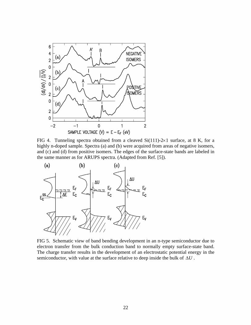
and negative) domain abundance. By neglecting cross-section effect completely, one would conclude that the relative abundance of positive and negative domains varies considerably from sample to sample, at least by a factor of four. Given our interpretation of the peaks (peak A arising from filled states of positive isomers, and A'/B from filled/empty states of negative isomers), it is not surprising that the relative energy separation of peaks A' and B remains constant, since that separation is essentially just the energy gap of negative isomers. 3 To interpret the variation in separation between A and A', on the other hand, we argue in Section III(C) that an electrostatic effect associated with electronic charge transfer from positive- to negative-isomer domains is varying. We demonstrate there that self-consistency of the charge transfer leads to a variation in electrostatic potential between the domains, such that the energy of the empty surface-state band for the positive isomers becomes nearly equal to that of the negative isomers (even though it starts out above that of the negative isomers, prior to the charge transfer). That situation would correspond to Fig. 3(a), with the filled band A attaining its lowest energy position. In the other cases [Figs. 3(b) and 3(c)], we argue that less charge transfer from the positive to the negative isomer domains occurs, due to smaller domain sizes on the cleaved surface, with the consequence of a higher energy position for the filled band A. Additional information coming from the ARUPS experiments regards the effect on the spectra of residual gas contamination. We have observed in a number of cases (not shown here) that whenever a contamination of the clean surface occurs (due to time elapsing, or switching on a pressure gauge, or intentional oxidation), besides a marked decrease of peak B, the areal ratio A'/A decreases, i.e. the number of negative isomers decreases. One possible interpretation of these observations is that the sticking-coefficient differs between the two types of isomers (e.g. because of possibly different energetic positions of the electrons involved). However, as argued below, we can also interpret these effects in terms of an increased number of contamination-induced electronic states at the domain boundaries, which lead to a reduction in the energy gain produced by charge transfer from the positive to the negative isomers (that is, the negative isomers become less energetically favorable, and so some of them convert to the positive isomer structure). The prior LT-STM work is completely consistent with the LT-ARUPS work in that it reveals the co-existence of negative and positive isomer domains, with roughly comparable abundances, on the surface. Reference [5] showed neighboring positive and negative domains, separated by a relatively well-ordered domain boundary. On a larger scale, the surface consists of interspersed domains of the two isomer types, with typical dimension for a domain of ≈7 nm. Figure 1(c) provides a sketch of the coverage of the domains on the surface, based on a series of voltage-dependent STM image of the same surface presented in Ref. [5]. It should be emphasized that most of the boundaries between different domains of the 2×1 reconstruction appear to be pinned in location by
3 The observed B peak actually arises from the low-energy tail of the empty-state surface band (at the J-point), so the observed separation is not exactly the same as the energy gap, but rather, it is closely related to the gap.
6
adsorbates, and hence the boundaries are immobile as a function of temperature (a few domain boundaries on the surface with quite specific structure might be mobile at room temperature or below, as reported in Ref. [9] and also occasionally observed by us, but the vast majority appear to be pinned by adsorbates). An important result from the LT-STM work is that the onset of the empty surface-state band for the negative isomers is found to be slightly below that of the positive isomers. The spectra from Ref. [5] are reproduced in Fig. 4, showing results from two locations within negative isomer domains and two from positive isomer domains. Reproducibility of the results for each isomer type is reasonably good. The surface states on either side of the surface band gap are marked by the thin vertical lines and labeled in the same manner as the ARUPS spectra: the edge of the filled states for positive isomer is denoted by A, the edge of the filled state for negative isomers by A', and the edge of the normally empty states for negative isomers by B (no label is provided for the empty states of the positive isomers since this state is not visible in ARUPS, being empty even for high doping). The edge of the empty states for the positive isomers is fairly well defined in the STS data of Fig. 4, but for the negative isomers that band edge occurs very close to 0 V and it is sometimes obscured [e.g. in Fig. 4(b)] by the fact that a minimum in the conductance occurs at 0 V due to a Coulomb gap, as previously described by Garleff et al. (for positive isomers) [7]. Nevertheless, even with this uncertainty, the edge of the empty surface-state band for the negative isomers can be seen to be lower than that of the positive isomers, by ≈0.07 eV. Another notable feature in the spectra is the significant amount of conductance seen at energies within the surface band gap, for both isomer types. This midgap conductance was attributed in the prior work of Garleff et al. to surface disorder [7]. We agree for the most part with that identification, although we return to further discuss this issue in Section IV. To account for the sample-to-sample variation seen in the ARUPS spectra, we propose that the average size of isomer domains is changing between samples. This type of variation is not surprising for surface preparation by cleavage; variation in the optical flatness is seen between different samples, and that apparent flatness is certainly related to surface step density which itself affects the 2×1 domain size. Even in the absence of surface steps, the 2×1 reconstruction leads of domains of certain size, depending on the stress-field on the surface during the cleavage. Prior STM studies have revealed domains of >100 nm extent for exceptionally good cleaves, decreasing to <10 nm for less ideal cleavage quality [10]. The samples examined by low-temperature STM in Ref. [5] had typical domain size of 7 nm, similar to the lower end of the range found in past work. III. Model of Charge Transfer between Domains A. Total Energies, including Electrostatics We examine here in more detail the mechanism proposed in Ref. [5] and mentioned above concerning a lower edge of the empty surface-state band for negative isomers providing a driving force for their formation. To this end, we compute the change in electronic energy of the system due to a redistribution of charge. We consider the
7
situation that occurs for our surfaces, with electrons transferring from the bulk conduction band (CB) to the empty surface-state band, as pictured in Fig. 5. Before any transfer, Fig. 5(a), the electric field is zero everywhere. For ease of discussion, we assume for the moment that the densities-of-states at the onsets of the CB and the empty surface-state band, energies CE and SS
CE , respectively, are very high so that all electrons transfer between those levels. Thus, for the first electron transferred, the change in total energy is 0<−=Δ C
SSC EEE . For subsequent electrons, an electrostatic potential energy
0>ΔU forms in the depletion layer of the semiconductor, as pictured in Fig. 5(b). In that case the change in electronic energy when an electron transfers is 0<Δ+Δ UE , and transfer of electrons continues until UΔ grows to a value such that 0=Δ+Δ UE , Fig. 5(c). To obtain the change in electronic energy we integrate the quantity UE Δ+Δ over all the charges transferred. For a differential number of electrons dn, we have an energy change of )]([ nUEdndEtot Δ+Δ= where UΔ is a function of the number of electrons transferred. We integrate totdE from 0 to tn where NLAnt = is the total number of electrons transferred, with N being the doping concentration, L the depletion length, and A the area. Integrating the EΔ term (which is a constant) gives simply 0<ΔEnt , which is the energy change without any consideration of the development of the electrostatic potential in the depletion layer. For the integral of the )(nUΔ term, we recognize that as being equal to the energy stored in the electric field distribution of the system (i.e. in analogy to the well known textbook example of the energy stored in a parallel plate capacitor [11]). Thus, we identify the total change in energy as being equal to
fieldlevelsenergyelec EEE Δ+Δ=Δ − (1) with the first term arising from the change in occupation of single-particle energy levels between initial and final states, and the second term being due to the development of the electric field distribution in the material. For the case at hand of the simple development of the depletion layer in the semiconductor, the integral of )(nUΔ in the second term gives a result of 03/ >Δ− Ent , yielding a net change in energy of 03/2 <ΔEnt . We generalize the result just described so that it applies to arbitrary densities-of-states in the bulk and surface bands and also to an arbitrary three-dimensional arrangement of electric fields. The first term in the electronic energy change is given by summing the single-particle energies ε times the difference in their occupation with and without the electrostatic potential energy )()( rr eVU −= where )(rV is the electrostatic potential. The second term is given by the energy in the electric field distribution. Thus, we have
dVddfUfDEelec ∫∫ ∫ +−+=Δ∞
∞−
20 )(2
)]())(([)( rErκε
τεεεεε τ (2)
where the τd integral is a volume or surface integral for bulk and surface states, respectively, and )(ετD is the density-of-states (DOS) per unit volume or per area, as appropriate (it is important to note that this DOS factor does not include any contribution
8
from the electrostatic potential that forms due to the charge transfer). In the second term, )(rE is the electric field, κ is the relative dielectric constant of the material, 0ε is the
permittivity of free space, and the integral extends over all space. We must include contributions from Eq. (2) from each spatial region: a bulk contribution from the first term for the change in electron occupation in the depletion region, a surface contribution from the first term for the occupation of the empty surface-state band, and the contribution from the energy in the fields from the second term. This latter contribution is positive, and taking the zero of energy for ε to be at the Fermi-level then the first contribution is negative and close to zero (for low temperatures) and the second contribution is negative and larger in magnitude than the first. We have evaluated Eq. (2) for some examples of surface state distributions. Initially, we consider empty surface-state bands that have constant DOS, and for positive isomers we take the onset of the empty surface-state band to be at eV6.0+= V
SSC EE (hence, with
bulk gap of 1.17 eV, the onset is at eV57.0−= CSSC EE ). The total number of states in
the band is 2/(0.255 nm2) where 0.255 nm2 is the area of a surface unit cell and the 2 in the numerator is for spin degeneracy. In this initial example we distribute those states over a 1 eV energy interval. We use an n-type doping concentration of 5×1018 cm-3 and assume a parabolic CB with density-of-states effective mass of 1.026 [12], yielding a Fermi-level for degenerate conditions of eV010.0+= CF EE . Transfer of electrons from the CB to the empty surface-state band is then considered, with the electrostatic potential computed by a finite-difference method previously described [13,14].4 The first entry of Table II shows the resulting change in electronic energy at temperature of 8 K for a 10×10 nm2 positive-isomer domain, computed according to Eq. (2). This result, −2.398 eV per 100 nm2, is approximately equal to the energy difference −0.57 eV times the number of electrons transferred, NLA , times 2/3 (from the contribution of the field energy as described above). The depletion length is approximately 5
nm3.12/)eV57.0(2 20 == NeL εε for doping concentration of -318 cm105× and
dielectric constant of 12.1, yielding 6.2 electrons transferred from the bulk to the surface for 100 nm2. The resulting estimate for the energy change is then −6.2×0.57×2/3 = −2.34 eV, which is close to the exact result −2.398 eV [their difference arising from the contributions of the complete DOS distributions and the occupation of those states, as in Eq. (2)]. 4 The finite-difference geometry considered in Refs. [13] and [14] includes the presence of a probe-tip in proximity to the semiconductor surface. In the present computations the separation between tip and sample is taken to be 100 nm, so that the tip has a negligible influence on the results. 5 This expression for L is approximate since the use of 0.57 eV as the barrier height neglects the differences of the Fermi-level position from both CE and SS
CE , i.e., in this simple estimate we are assuming very large DOS at the band edges.
9
We next consider a negative-isomer domain, taking its onset to be 0.3 eV lower than for the positive isomers (the reason for this choice will be made clear in the following Section). The second row of Table II shows the corresponding change in electronic energy, which is seen to be 2.126 eV lower (more negative) than for the positive isomers. This value represents an electronic driving force for the formation of the negative isomers, i.e. 5.4 meV per 2×1 unit cell. At a higher temperature of 300 K (Fermi-level at
eV041.0−CE ) the values for the energies associated with the charge transfer are slightly lower (more negative), as shown in the fourth and fifth rows of Table II. The reason for this change is that higher lying states are occupied due to the increased temperature, with the result for elecEΔ acquiring a temperature dependence since the DOS for the surface-state is not equal to that of the CB DOS (integrated over the depletion region). In terms of an energy difference, formation of the negative isomers is favored by 2.118 eV per 100 nm2 area, practically the same as for the 8 K results. The second column of Table II show results for a different surface DOS, the one for an ideal model of one-dimensional (1D) π-bonded chains [15]. In this model there are singularities in the DOS at the band edges (care has been taken in the computation to properly handle those singularities in all integrals, i.e. for the charge densities and electrostatic energies). The results at 8 K are nearly the same as those for the model of a uniform DOS, although the temperature dependence of the π-bonded chain results is slightly larger than for the uniform DOS (since the π-bonded chain DOS decreases with increasing energy, i.e. even more unlike the bulk CB DOS and hence favoring occupation of the surface-state at elevated temperatures). In terms of an overall distribution, the actual DOS for the 2×1 surface lies somewhere between the two models considered. However, in terms of the DOS near the onset of the empty surface-state band, which is the critical parameter in our computation, the model of constant DOS is certainly better (i.e. it provides a better match to a full DOS computed theoretically [5]), and so we use that model for all further computations. B. Co-existence of Positive and Negative Isomer Domains An important aspect of the experimental results is that the positive and negative isomers are observed to co-exist, i.e. in different domains. Why should this co-existence occur, that is, why is the surface not entirely composed of positive or negative isomers (whichever has lowest energy)? To explore this point, we perform computations for arrangements of alternating positive and negative isomer domains, as pictured in Fig. 6. Initially each domain is taken to have size 10×10 nm2. The difference between the lower edges of the empty surface-state bands between the isomers is taken to be eV3.0=Δ SS
CE , as in the previous Section. With these domains present on the n-type Si surface, charge transfer between bulk and surface is computed by a three-dimensional solution of Poisson's equation including occupation of bulk and surface states in accordance with a fixed Fermi-level FE . Arbitrary energy distributions and spatial arrangements of the surface states, )( Fi Eσ for the ith spatial region, can be easily handled in the finite-difference computation [13,14]; the electrostatic potential is obtained self-consistently with the spatially varying occupation of the surface states in a semiclassical
10
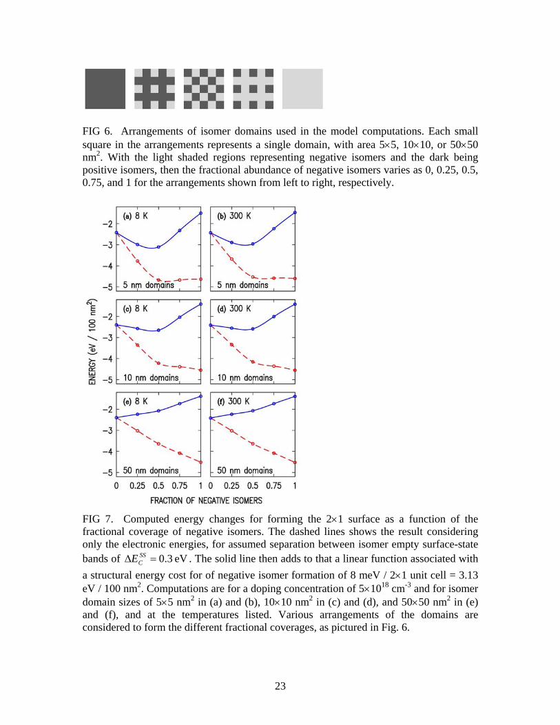
approximation, i.e. with surface state density given by ))0,,((),( yxUEyx Fi −= σσ where the ith region of space contains the point x,y and )0,,( yxU is the electrostatic potential energy at that surface point [16]. A corrugated type of band bending across the surface is thus obtained, with more band bending at the negative domains compared to the positive ones. Electronic energy changes for a checkerboard arrangement (50% negative, 50% positive isomers) are listed in Table II, for temperature of 8 and 300 K These results can be seen to lie significantly below the average of the values for purely positive or negative isomers on the surface. The reason for this energy reduction is that electrons from the positive domains are transferred to the negative ones, thus lowering the total energy of the system. For the 10×10 nm2 domains, about 5.0 electrons are found to transfer from the domain of positive isomers to the domain of negative isomers. The resultant energy reduction is compensated by an energy increase due to electron-electron repulsion within a domain, but for the 10-nm domains that effect is not large enough to cancel out the energy reduction. Additionally, lateral electric fields form at the domain boundaries, but those fields turn out to give only a small contribution to the total energies. The dashed lines in Fig. 7 shows plots of the electronic energy of our system as a function of the fraction of negative isomer coverage, for domain sizes of 5×5 nm2, 10×10 nm2, and 50×50 nm2. Again, the bowing of the curves near their center (for small domain sizes) arises from the favorable process of charge transfer from positive to negative domains. An additional important factor that will affect the energetics of the domains is the difference in structural formation energy between the two types of isomers. This value is quoted as 8 meV per 2×1 unit cell by Patterson et al., with the positive isomers lower in energy [17]. These values are referred to as total energies in that work, but since we are also considering the electrostatic plus single-particle CB energies, we refer to those values from Ref. [17] as structural formation energies and we add to those the results of Eq. (2) in order to arrive at a total energy,
strucelectot EEE Δ+Δ=Δ . (4) Thus, to obtain a total energy, one must add to the dashed lines of Fig. 7 a strucEΔ function that varies linearly with the fraction of negative isomers. We choose in Fig. 7 a structural formation energy equal to the value of Patterson et al., 8 meV / 2×1 unit cell = 3.13 eV / 100 nm2 [17]. This choice produces negative isomers that are unstable (larger
totE for negative isomers than for positive ones) for the doping concentration of 5×1018 cm-3, since the 3.13 eV energy cost for forming the negative isomer domain is greater than the 2.398 eV gain in electronic energy produced by our assumed band offset of 0.3 eV. However, a minimum in energy for the system occurs when the isomer domains co-exist, for sufficiently small domains as seen in Fig. 7, in agreement with the experimental results. Performing similar computations for the case of 300 K produces the results shown on the right-hand side of Fig. 7. We find that the occurrence of the negative isomers is slightly less favorable than at 8K, for the reason given in the previous Section. Regarding a doping dependence of the results, this arises from the fact that the number of electrons
11
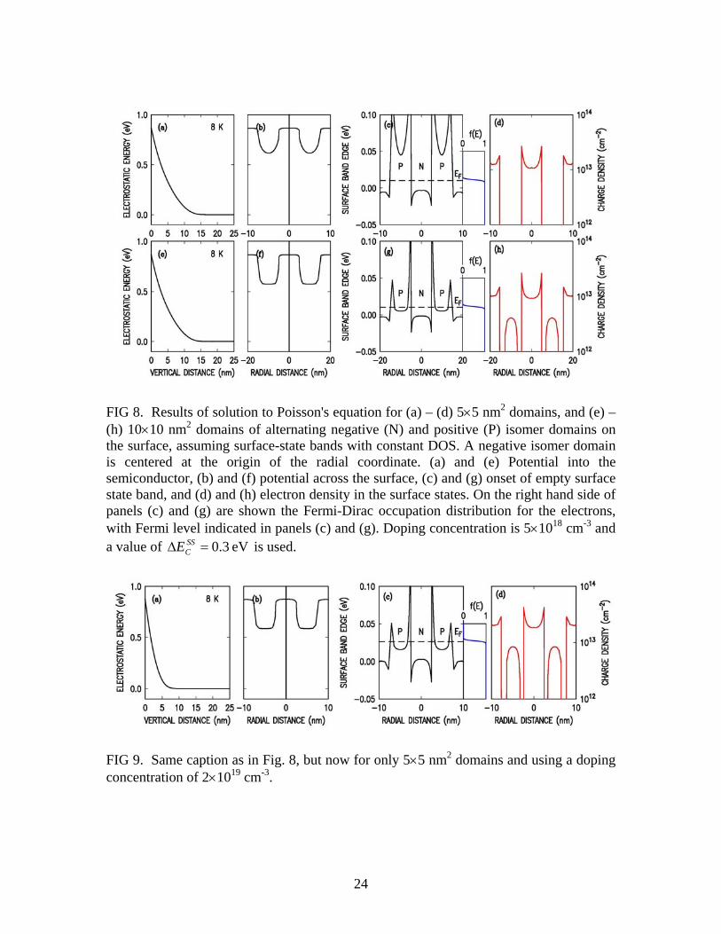
transferred from bulk to surface, and hence the energy gain, is proportional to the square root of the doping concentration, N. Hence the dashed lines in Fig. 7 vary as N .6 However, the correction due to strucEΔ is independent of N. Thus for a smaller doping concentration than that considered in Fig. 7 a complete coverage of positive isomers would be energetically favorable, and for a larger concentration a complete coverage of negative isomers are favorable. The doping concentrations for these situations to occur are found to be, e.g., 2.5×10¹⁸ and 1.8×1020 cm-3, respectively, for a domain size of 10×10 nm2. This agreement between the experiment and the model in terms of the co-existence of positive and negative domains, and of their doping dependence, provides, we believe, compelling evidence that this model of electrostatic charge transfer between domains is indeed an appropriate description of the physical system and provides the reason for the existence of the negative isomers. In our analysis thus far we have used the structural formation energy from theory [17], and employed a band offset of 0.3 eV chosen such that negative isomers are energetically favorable only for domain sizes of ≲10 nm. This results is agreement with experiment, not only for the actual existence of the negative isomers, but also in terms of the variation in their number and their ARUPS lineshapes as seen from sample to sample as discussed in Section II. C. Further Comparison of Experiment and Theory In the previous Section we employed the results of Fig. 7 for the abundance of isomers vs. domain size to draw conclusions about the magnitude of the energy offset between empty surface-state bands of the negative and positive isomers. However, a separate means by which we can examine the band offset is through the ARUPS and STS data. Experimentally, the STS data reveal an apparent offset between the empty surface-state bands that is about 0.07 eV lower for the negative isomers than for the positive ones [5]. The ARUPS data reveal significant sample-to-sample variation in the energies of the surface states, which we associated in Section II with a variation in domain size. We compare these results to our model predictions by explicitly plotting the electrostatic potential on surfaces with alternating domain types. It is important to understand in this regard that the band offset seen in the experiment is influenced by charge transfer between the positive- and negative-isomer domains, which tends to raise the electrostatic potential energy of the negative domains (since they become negatively charged). This same effect is also present in our model, since all of our computations are fully self-consistent. Figure 8 shows results of our computations for 50% coverage of negative domains, with domain sizes of 5×5 and 10×10 nm2 [i.e. same parameters as in Figs. 7(a) and 7(c)]. Since the edge of the surface-state band for the negative isomers is lower than for the positive ones, then more of the electrons end up occupying the negative isomer surface-state band,
6 Additionally, the amount of bowing that occurs in Fig. 7 at 50% isomer coverage is gradually reduced as N increases.
12
producing a higher electrostatic energy in the negative isomer domains. For the 10×10 nm2 domains, this electrostatic energy shift is nearly equal to the difference in band edge energies (0.3 eV), so that for most of the spatial area within the center part of the positive or negative domains their empty surface-state band edges turn out to be at nearly the same energies, within about 5 meV [Fig. 8(g)]. However, for the 5×5 nm2 domains, a much larger apparent offset between their band edges occurs, about 70 meV averaged over the domain areas [Fig. 8(c)]. We thus predict a variation in the location of the surface state bands for the positive isomers of many 10's of meV, depending on the size of the isomer domains. This result is consistent with the ARUPS results of Fig. 1, where a variation of up to 50 meV in the relative positions of the A and A' bands is found (the doping densities for the ARUPS sample of Fig. 1 were 4×10¹⁸ and 8×1018 cm-3, close to the 5×1018 cm-3 used for the computations of Fig. 8). It should also be noted that, for the positive isomers, a significant variation in the potential occurs across the domains. Hence photoemission lineshapes for states originating from the positive isomers would be expected to be broadened, in agreement with the observations discussed in Section II. Considering now the STS data, the doping density in those samples was 2×1019 cm-3, so that, even with the charge transfer from positive to negative domains, the positive domains do not become fully depleted. Results are shown in Fig. 9 for 5×5 nm2 domains. The band edge on the positive domains is well below the Fermi-level, and it is separated from that on the negative domains, over most of the domain areas, by only about 15 meV. For 10×10 nm2 domains (not shown) the band edges are even closer, within 7 meV. Thus, we obtain a result that is in contradiction of the STS data, which reveal an apparent offset between bands of about 70 meV. To resolve this problem we consider the possible role of defects on these surfaces. Boundaries between domains could give rise to electronic states, as could adsorbates on the surface (the STM images do indeed reveal a significant adsorbate density [5]; these defects need not necessarily be contamination, but rather, could be stray Si atoms arising from the relatively small domain size). We introduce extrinsic acceptor-like states associated with these defects into the model, placing these states deep in energy so that they are always filled with electrons. With only 0.01 monolayer [ML = 1/(2×1 unit cell area) = 1/(0.384×0.665 nm2) = 3.916 nm-2] of extrinsic states, the number of electrons in the surface bands drops to the same value as for the 5×1018 cm-3 doping concentration. We have fully modeled this situation, and we obtain results for the electrostatic potential (and for total energies) that are very similar to those of Fig. 8 for the 5×1018 cm-3 doping case in the absence of any extrinsic states. Thus, a value for SS
CEΔ of 0.3 eV produces results in agreement with the observed ARUPS and STS spectra (assuming a small number of extrinsic states in the latter case, consistent with the STM images). This band offset, together with the structural energy of
≈strucE 8 meV per 2×1 unit cell taken from theory [17], also produce good agreement with the doping-dependence of the abundance of negative isomer domains. This latter point is examined in more detail in the following Section. Regarding the 0.3 eV band offset, it is significantly greater than the values of 0.07 or 0.09 eV predicted by first-principles theory [5,17], although the difficulties of density-functional theory in predicting band gaps are well known [18].
13
We have modeled a number of other situations, in an effort to investigate uncertainty of our SS
CEΔ result. Let us first consider a smaller SSCEΔ value of 0.1 eV. In that case, the
results for the electronic energies in Fig. 7 (dashed lines) are reduced by about a factor of 3 (i.e. proportional to SS
CEΔ ). In order to achieve consistency in isomer abundance with experiment it would then be necessary to also decrease the value of strucEΔ used, by the same factor of 3. That value for strucEΔ would be inconsistent with the most recent theoretical prediction [17] (although that prediction also differs from earlier values as discussed in Ref. [17], illustrating the difficulty in such calculations). In any case, determining parameter values solely from the experimental data, the reduced values for
SSCEΔ and strucEΔ would also be inconsistent with the ARUPS and STS spectra that
reveal depletion of electrons from the positive isomer domains (for sufficiently small domains). To further study this limit on the reduced values of SS
CEΔ and strucEΔ , we have performed computations for a wide range of models that include extrinsic states. In general, such states act to deplete electrons from the isomer domains. Hence it might seem possible that consistency of experiment and theory in terms of the depletion could be possible for a sufficiently large number of extrinsic states. However, we find that this is not the case. In particular, for the doping concentration of 2×1019 cm-3 and maintaining =Δ SS
CE 0.1 eV, we consider larger and larger numbers of extrinsic states (placing them either uniformly over the surface, or specifically at domain boundaries) such that depletion of the positive domains occurs. For a domain size of 5×5 nm2, we find the expected depletion of the positive domains for a defect density of about 0.01 ML. However, in this case we find that the total energy of the system of intermixed negative and positive domains is unfavorable, i.e. the entire surface will convert to positive domains, the reason being that transfer of electrons from positive isomers to the extrinsic states yields a greater reduction in total energy than transfer from negative isomers to extrinsic states. No matter what model for the extrinsic states we employ, we find that it is not possible to simultaneously fit all the experimental data for a value of SS
CEΔ near 0.1 eV. A value of 0.2 eV is similarly found to fail, but not by such a large margin as the 0.1 eV value. A value of 0.3 eV works well, as illustrated in Figs. 7 and 8. Let us now consider a larger value for SS
CEΔ . Returning again to the plots of Fig. 7, this increased value of SSCEΔ
would have to be compensated by an increased value of strucE . Regarding the depletion of positive domains apparent in the ARUPS and STS data, the precise domain sizes in the former and the actual density of extrinsic states in the latter are both unknown, so the observed depletion cannot be used to produce an upper bound on SS
CEΔ . However, it seems unlikely that SS
CEΔ would be much larger than 0.3 eV based on the observed band gaps of the negative and positive domains of 0.47 and 0.83, respectively [5] (both with uncertainty ±0.07).
14
An additional effect that we have considered is the detailed form of the surface-state DOS near the band edge. As mentioned at the end of Section III(A) we feel that a uniform DOS (as used for the computations of Figs. 7 – 9) is better than a singular DOS at the band edge. Actually, if we use the latter, then the depletion of the positive isomer domains actually decreases slightly. Considering the opposite situation of a very small and slowly increasing DOS at the surface-state band minimum, we expect that that would produce a slightly larger apparent offset between band edges than in Fig. 8, but this result would not be anywhere near the experimental value. We have also considered the influence of the discrete dopant atoms on the surface potential. For example, for the doping concentration of 5×1018 cm-3 there are only 6 – 7 dopants within the depletion region beneath each 10×10 nm2 surface domain. Statistical variation in that number might be significant (i.e. as found for bulk semiconductor devices [19]). In our theory, the bulk doping is usually modeled in a spatially uniform way. To treat the variation in doping, we decompose the bulk into 10×10×10 nm3 cubic regions of alternating doping concentration of 3×1018 cm-3 and 7×1018 cm-3. We then place a positive isomer domain over a low-doped region and a negative domain over a high-doped region, to see if the resultant apparent band edge difference in the theory might be increased. The resultant shift of apparent band edges in the theory changes by <4 meV, which again is a very small effect. In conclusion, the comparison of experiment with our model computations can probably best be summarized by employing the structural formation energy from first-principles theory, 8 meV per 2×1 unit cell [17]. With that, we can confidently conclude from our analysis that the band offset SS
CEΔ is 0.3 eV, with an uncertainty of < 0.1 eV. IV. Discussion The results of the model computations of Section III, for the parameter values assumed there, provide a good description of most of the experimental results summarized in Section II. Consider first the ARUPS data of Ref. [5], obtained from samples with 4×10¹⁸ and 8×1018 cm-3 doping concentration. Co-existence of positive and negative isomer domains is clearly evident in the spectra, although the relative abundance as well as the detailed ARUPS lineshapes vary from cleave to cleave. The results of the STM/S measurements of Ref. [5] also yield a mixture of domain types, for doping of 2×1019 cm-3. All of these results are in agreement with our model predictions shown in Fig. 7 and summarized in Fig. 2(b) (i.e. taking into account the domain size for the surfaces studied by STM/S, which is < 10×10 nm2). Two samples are apparent in Fig. 2(a) that do not appear to match the other experimental studies nor the model predictions, namely, the STM/S results of Nie and Feenstra in Ref. [6] and of Garleff et al. in Ref. [7]. In the former case, negative isomers would be expected based on the very high doping concentration. Those measurements were conducted at room temperature, and there is some disagreement even in other data concerning the temperature dependence of the negative isomer abundance. The ARUPS
15
results of Ref. [5] revealed, in general, reduced amounts of negative isomers as the temperature was increased, but it is difficult to separate this effect from the role of contamination (which invariably occurs when a sample holder is warmed up) which itself will cause a drop in the number of negative isomers. For the case of Ref. [6], relatively large domains were studied, which would tend to favor positive isomers. Additionally, residual contamination, even though it is not evident in the STM images [6], could possibly also favor the formation of positive isomers. STS measurements that would directly reveal the electron occupation of the normally empty surface-state band were not performed along with the STM measurements of Ref. [6]; future work that includes such measurements would be useful. Regarding the observations of Garleff et al. [7], they have reported only a single isomer type, and based on the observed band gap in their STS data those appear to be positive isomers. We would expect negative isomers for their data, based on the doping concentration of 6×1018 cm-3. We note that the occupation of the empty surface-state band in their data is very substantial, indicating minimal amounts of surface contamination. It should also be noted that the size of the 2×1 domains on their surfaces is relatively large (at least compared to that in the STM data of Ref. [5]) [20]. In this case, the domains might indeed be large enough, compared to those of the ARUPS samples of Ref. [5], so the positive domains are energetically favorable [i.e. as in the case of Fig. 7(e)]. Again, further work on similar samples, including measurements over a range of domain sizes, would be useful to more fully understand the situation. Finally, we return to further consider the STS spectra, highlighting one aspect of them that may or may not be relevant to the negative isomer formation but nonetheless appears to be quite interesting. We speak of the midgap conductance found in the spectra, as shown in Ref. [5] and also pictured in Fig. 4. This midgap conductance was previously identified by Garleff et al. as arising from surface disorder (e.g. near point defects such as dopant atoms [21,22], and also, presumably, near domain boundaries), with the spectral shape also influenced by a Coulomb gap near 0 V [7]. Their surfaces revealed only positive isomers, and an intense band of midgap states was found for those isomers. In contrast, the surfaces of Ref. [5] showed both isomer types, with the midgap conductance being relatively weak for the positive isomers [Fig. 4(d) gives a typical spectrum] but quite intense for the negative isomers. The negative isomer domains also display a much higher electron concentration (lower band edge for empty surface states) than at the positive isomer domains. In fact, a strong correlation was found between the intensity of the midgap features and the electron concentration [5]. This type of correlation is very unusual in STS data; normally, a high electron concentration on a surface would not, itself, induce new states (rather, the electrons would just occupy existing states). For this reason, we consider it quite possible that the midgap "disorder-induced" states discussed by both Garleff et al. and in our prior work might, in fact, have a somewhat different origin, e.g. some sort of multi-particle excitation produced by the high electron concentration at the surface. A possible multi-particle effect that would produce midgap states is a surface polaron (coupled electron and phonons), as discussed previously by Chen et al. [23]. Those
16
authors assumed dimerization of the π-bonded chains in their analysis. Such dimerization is now thought not to occur for perfect π-bonded chains, on the basis of the work of Alerhand and Mele, but, importantly, this sort of distortion of the chains is in fact very close to occurring [24]. Thus, near defects, dimerization might well be present, and if so, then for highly-doped samples a state split-off from the empty surface-state band could result. We speculate that the intense midgap states observed in the STS spectra arise from this sort of mechanism. Future work, involving detailed voltage-dependent STM images (i.e. looking for shift in the corrugation phase in a direction along the π-bonded chains) would be useful to further investigate the origin of the midgap states. Even if such polarons are present, they will not necessarily have a significant impact on the negative isomer formation. However, the possible presence of surface polarons is certainly interesting in and of itself. For example, the existence and temperature-dependence of a surface polaron would likely impact the magnitude of the Si(111)-2×1 surface bandgap observed by room temperature STS [3,25] and a complete set of temperature-dependent spectra bridging the present 8 K and 300 K results are needed to investigate that possibility. V. Summary In summary, we have presented new data relating to the co-existence of negative and positive isomers on the Si(111)-2×1 surface. For a given doping concentration, we argue that the size of isomer domains affects the relative abundance of the isomer types. A model is presented that evaluates the total energy change of charge transfer from bulk to surface and between domains on the surface. There are two parameters in this model: the offset between empty surface-state band edges of the negative and positive isomers,
SSCEΔ , and the structural formation energy of the negative isomers relative to the positive
ones, strucEΔ . Considering the experimental data for the abundance of isomer types we argue that the values of these parameters are correlated: a structural formation energy of 8 meV / 2×1 unit cell implies a band offset of 0.3 eV, whereas a formation energy of about 2.7 meV implies an offset of 0.1 eV. In other words, the ratio of strucEΔ to SS
CEΔ is 0.027, a result that we have determined from our analysis to an accuracy of better than 30%. To further constrain the parameter values we can employ the formation energy from first-principles theory of 8 meV [17], thus yielding a band offset of 0.3 eV. An independent constraint on the values can be obtained by examination of the data for the depletion of charge from positive domains. From that, we find a best-fit band offset of 0.3 eV, thus implying a formation energy of 8 meV. This agreement in the results for the formation energy between the first-principles theory and the analysis based solely on experimental data provides us with some additional confidence in the numerical results. One point to consider in our model for the isomer abundance is the rather small energetic differences between the various domain arrangement on the surface, e.g. a total energy difference (including electronic and structural components) on the order of 0.2 eV / 100 nm2 domain = 0.5 meV / 2×1 unit cell. Although these energies per domain are large enough, e.g. compared to Tk , to account for the experimental observations, it remains to be determined how the surface can actually switch from one domain type to the other, e.g. as temperature is varied (entropic effects at higher temperatures might also be important).
17
Future theoretical work on the energy barriers involved would be most useful in addressing this issue. Acknowledgements The work was been supported by the U.S. National Science Foundation and by the A. v. Humboldt Foundation. We thank J. K. Garleff for providing us with a copy of the relevant sections of Ref. [20] and P. Gargiani for valuable assistance in taking the ARUPS data. Discussions with J. H. Davies are gratefully acknowledged. The experimental LT-STM studies which led, in part, to the development of the model described herein were performed during 2001 in the laboratory of K. H. Rieder at the Free University of Berlin, while one of us (R.M.F.) was visiting there. We are grateful to Prof. Rieder for making that research visit possible, and we acknowledge G. Meyer for his invaluable contributions to the research during that period. We all wish Prof. Rieder the very best on this occasion of his 70th birthday.
18
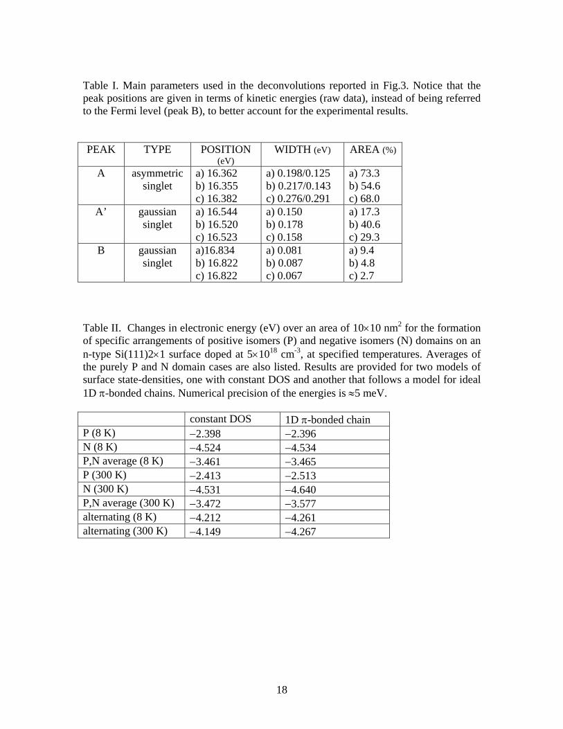
Table I. Main parameters used in the deconvolutions reported in Fig.3. Notice that the peak positions are given in terms of kinetic energies (raw data), instead of being referred to the Fermi level (peak B), to better account for the experimental results. PEAK TYPE POSITION
(eV) WIDTH (eV) AREA (%)
A asymmetric singlet
a) 16.362 b) 16.355 c) 16.382
a) 0.198/0.125 b) 0.217/0.143 c) 0.276/0.291
a) 73.3 b) 54.6 c) 68.0
A’ gaussian singlet
a) 16.544 b) 16.520 c) 16.523
a) 0.150 b) 0.178 c) 0.158
a) 17.3 b) 40.6 c) 29.3
B gaussian singlet
a)16.834 b) 16.822 c) 16.822
a) 0.081 b) 0.087 c) 0.067
a) 9.4 b) 4.8 c) 2.7
Table II. Changes in electronic energy (eV) over an area of 10×10 nm2 for the formation of specific arrangements of positive isomers (P) and negative isomers (N) domains on an n-type Si(111)2×1 surface doped at 5×1018 cm-3, at specified temperatures. Averages of the purely P and N domain cases are also listed. Results are provided for two models of surface state-densities, one with constant DOS and another that follows a model for ideal 1D π-bonded chains. Numerical precision of the energies is ≈5 meV. constant DOS 1D π-bonded chain P (8 K) −2.398 −2.396 N (8 K) −4.524 −4.534 P,N average (8 K) −3.461 −3.465 P (300 K) −2.413 −2.513 N (300 K) −4.531 −4.640 P,N average (300 K) −3.472 −3.577 alternating (8 K) −4.212 −4.261 alternating (300 K) −4.149 −4.267
19
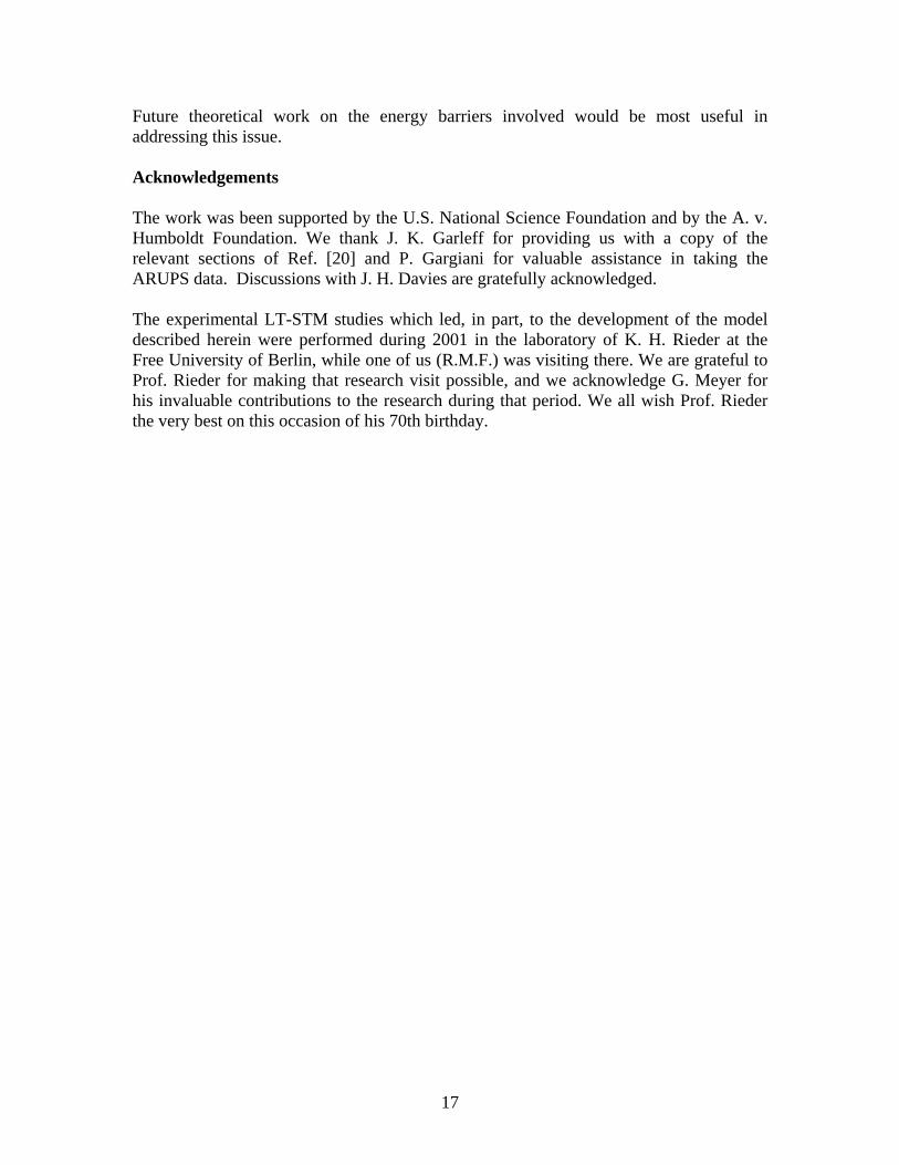
FIG 1. (a) Schematic models for positively-buckled isomers and negatively-buckled isomers of the π-bonded chain structure. Surface atoms with predominantly filled dangling bonds are marked by solid circles, and those with empty dangling bonds are shown by open circles. The former are mainly sp3-coordinated and the latter sp2-coordinated, giving rise to their vertical displacements above or below, respectively, the plane of the top layer atoms. (b) Schematic view of the surface-state bands associated with the π-bonded chains of Si(111)-2×1: filled band (π) and empty band (π*), with the lower edge of the empty band occurring at different energies for the two isomer types (indicated by SS
CEΔ ). The labels A, A', and B on the surface state features are the same as used for the ARUPS spectra. (c) Schematic view of large-scale arrangement of surface domains of positive (P) and negative (N) isomers, based on LT-STM studies of the surface, Ref. [5]. The right-hand half of the schematic extends over the same area as Fig. 2(a) of Ref. [5].
20
FIG 2. Schematic phase diagrams showing the presence of positive (P), negative (N), or mixed positive and negative (P+N) isomer domains on the Si(111)-2×1 surface. (a) Summary of experimental results, from the sources cited. (b) Predictions based on the model of the present work, assuming a domain size of 10×10 nm2 and values of
=Δ SSCE 0.3 eV and =Δ strucE 8 meV / 2×1 unit cell (see text).
21
FIG 3. Panels (a), (b), (c): various ARUPS spectra from different Si(111)-2x1 cleaved surfaces, at T=100 K, for a highly n-doped sample. Deconvolutions of the experimental curves performed with symmetric Gaussian for peaks A' and B, and an asymmetric Gaussian for A, are also shown. A lineshape variation is apparent, with peak A moving closer to A' and B (whose relative distance is fixed, within experimental uncertainty), going from (a) to (c). For this reason, the three curves a, b and c are also labeled with the energy difference ΔEAA’. The marked variation of ΔEAA’ in the three cases is ascribed to different amounts of charge transfer between isomer domains of opposite type, as stated in the text. Panel (d) shows an overview of the energy separations ΔEBA’ and ΔEA’A, as obtained by deconvolving spectra recorded in different cleaves. The spectra of the panels (a), (b), and (c) are identified by arrows. The dotted lines provide guides for the eye.
22
FIG 4. Tunneling spectra obtained from a cleaved Si(111)-2×1 surface, at 8 K, for a highly n-doped sample. Spectra (a) and (b) were acquired from areas of negative isomers, and (c) and (d) from positive isomers. The edges of the surface-state bands are labeled in the same manner as for ARUPS spectra. (Adapted from Ref. [5]).
FIG 5. Schematic view of band bending development in an n-type semiconductor due to electron transfer from the bulk conduction band to normally empty surface-state band. The charge transfer results in the development of an electrostatic potential energy in the semiconductor, with value at the surface relative to deep inside the bulk of UΔ .
23
FIG 6. Arrangements of isomer domains used in the model computations. Each small square in the arrangements represents a single domain, with area 5×5, 10×10, or 50×50 nm2. With the light shaded regions representing negative isomers and the dark being positive isomers, then the fractional abundance of negative isomers varies as 0, 0.25, 0.5, 0.75, and 1 for the arrangements shown from left to right, respectively.
FIG 7. Computed energy changes for forming the 2×1 surface as a function of the fractional coverage of negative isomers. The dashed lines shows the result considering only the electronic energies, for assumed separation between isomer empty surface-state bands of eV3.0=Δ SS
CE . The solid line then adds to that a linear function associated with a structural energy cost for of negative isomer formation of 8 meV / 2×1 unit cell = 3.13 eV / 100 nm2. Computations are for a doping concentration of 5×1018 cm-3 and for isomer domain sizes of 5×5 nm2 in (a) and (b), 10×10 nm2 in (c) and (d), and 50×50 nm2 in (e) and (f), and at the temperatures listed. Various arrangements of the domains are considered to form the different fractional coverages, as pictured in Fig. 6.
24
FIG 8. Results of solution to Poisson's equation for (a) – (d) 5×5 nm2 domains, and (e) – (h) 10×10 nm2 domains of alternating negative (N) and positive (P) isomer domains on the surface, assuming surface-state bands with constant DOS. A negative isomer domain is centered at the origin of the radial coordinate. (a) and (e) Potential into the semiconductor, (b) and (f) potential across the surface, (c) and (g) onset of empty surface state band, and (d) and (h) electron density in the surface states. On the right hand side of panels (c) and (g) are shown the Fermi-Dirac occupation distribution for the electrons, with Fermi level indicated in panels (c) and (g). Doping concentration is 5×1018 cm-3 and a value of eV3.0=Δ SS
CE is used.
FIG 9. Same caption as in Fig. 8, but now for only 5×5 nm2 domains and using a doping concentration of 2×1019 cm-3.
25
References 1 D. Haneman, Phys. Rev. 121, 1093 (1961). 2 K. C. Pandey, Phys. Rev. Lett. 47, 1913 (1981); 49, 223 (1982). 3 G. Bussetti, C. Goletti, P. Chiaradia, and G. Chiarotti, Phys. Rev. B 72, 153316 (2005),
and references therein. 4 M. Rohlfing, M. Palummo, G. Onida, and R. Del Sole, Phys. Rev. Lett. 85, 5440 (2000). 5 G.Bussetti, B.Bonanni, S.Cirilli, A.Violante, M.Russo, C.Goletti, P.Chiaradia, O.Pulci,
M.Palummo, R.Del Sole, P.Gargiani, M.G. Betti, C. Mariani, R.M. Feenstra, G. Meyer, and K.H. Rieder, Phys. Rev. Lett. 106, 067601 (2011).
6 S. Nie, R. M. Feenstra, J. Y. Lee, and M.-H. Kang, J. Vac. Sci. Technol. A 22, 1671 (2004).
7 J. K. Garleff, M. Wenderoth, R. G. Ulbrich, C. Sürgers, and H. v. Löhneysen, Phys. Rev. B 72, 073406 (2005).
8 P. Mårtensson, A. Cricenti, and G. V. Hansson, Phys. Rev. B 32, 6959 (1985). 9 P. Studer, S. R. Schofield, G. Lever, D. R. Bowler, C. F. Hirjibehim, and N. J. Curson,
Phys. Rev. B 84, 041306 (2011). 10 R. M. Feenstra and M. A. Lutz, Surf. Sci. 243, 151 (1991). 11 E.g. D. Halliday, R. Resnick and J. Walker, Fundamentals of Physics, 5th ed. (Wiley,
New York, 1997), p. 637. 12 Data in science and technology: Semiconductors, O Madelung ed. (Springer, Berlin,
1991). 13 R. M. Feenstra, J. Vac. Sci. Technol. B 21, 2080 (2003). 14 R. M. Feenstra, S. Gaan, G. Meyer and K. H. Rieder, Phys. Rev. B 71, 125316 (2005). 15 R. Del Sole and A. Selloni, Phys. Rev. B 30, 883 (1984). Note that Eq. (13) of this
work has a typographical error, the cosine term should be squared. 16 See http://www.andrew.cmu.edu/user/feenstra/semitip_v6/. 17 C. H. Patterson, S. Banerjee, and J. F. McGilp, Phys. Rev. B 84, 155314 (2011). 18 A. J. Cohen, P. Mori-Sanchez, and Y. Weitao, Phys. Rev. B 77, 115123 (2008), and
references therein. 19 G. Slavcheva, J. H. Davies, A. R. Brown, and A. Asenov, J. Appl. Phys. 91, 4326
(2002). 20 J. K. Garleff, Master's Thesis, University of Gottingen, 2001. 21 T. Trappmann, C. Sürgers, and H. v. Löhneysen, Europhys. Lett. 38, 177 (1997). 22 J. K. Garleff, M. Wenderoth, R. G. Ulbrich, C. Sürgers, H. v. Löhneysen, and M.
Rohlfing, Phys. Rev. B 76, 125322 (2007). 23 C. D. Chen, A. Selloni, and E. Tosatti, Phys. Rev. B 30, 7067 (1984). 24 O. L. Alerhand and G. Mele, Phys. Rev. B 37, 2536 (1988). 25 R. M. Feenstra, Phys. Rev. B 60, 4478 (1999).