ECS Journal of Solid State Science and Technology, 4 (9) P337-P346 (2015) P337
Charge Transport in Uniform Metal-Assisted Chemical Etching for3D High-Aspect-Ratio Micro- and Nanofabrication on SiliconLiyi Li,a Xueying Zhao,a and Ching-Ping Wonga,b,z
aSchool of Materials Science and Engineering, Georgia Institute of Technology, Atlanta, Georgia 30332, USAbDepartment of Electronic Engineering, The Chinese University of Hong Kong, Hong Kong
Manuscript submitted March 24, 2015; revised manuscript received June 29, 2015. Published July 22, 2015.
Fabrication of micro- and nanostructures on silicon (Si) is a keystep in manufacturing of modern electronic and optoelectronic de-vices. Especially, the high-aspect-ratio (HAR) structures, of which thevertical dimension is much larger than the lateral dimension, enableorders-of-magnitude higher integration density and superior systemperformance compared to that of traditional planar structures by uti-lizing the space inside Si. HAR structures, such as deep trenches anddeep holes, have been widely used in advanced Si-based devices. Forexample, deep trenches are the core structures in the microelectrome-chanical systems;1 deep holes serve as the interconnect routes in theemerging 3D integration technology in microelectronic packaging.2
Most of these HAR structures are fabricated by selective removal ofcertain volume of Si from the bulk Si substrate, which is generally re-ferred to as the etching of Si. Until now, the major applicable Si etchingmethod for HAR structures fabrication is the deep reactive ion etching(DRIE).3,4 In DRIE, Si is put in a gas chamber and etched by plasma.Although DRIE is able to fabricate a wide range of HAR structures, itis suffered from high cost. On the other hand, metal-assisted chemicaletching (MaCE), a novel low-cost wet chemical etching method, hasattracted attention from both academia and industry.5–8 In MaCE, athin layer of noble metal is deposited on top of Si. When the metal-loaded Si substrate is immersed in a hydrofluoric acid (HF)-hydrogenperoxide (H2O2) mixture solution, H2O2 is catalytically reduced onthe metal surface and electron holes (h+) are generated. With the pres-ence of h+, Si underneath the metal catalysts is etched by HF. MaCEfor fabrication of HAR nanostructures on Si, such as nanowires,9–16
nanogratings17 and nanopores,18 have been extensively studied. Re-cently, capability of MaCE in fabricating uniform micrometer-scaleHAR structures was demonstrated.19–22
The geometry of HAR structures in the 3D space plays the keyrole in the performance of the devices where they are involved. Thus,controllability over the 3D geometry of the etching profile (referredto as “3D profile” in the following discussion) is essential for anyHAR Si etching method. In DRIE, the 3D profile can be controlled bythe chemistry of plasma.4,23 In MaCE for nanostructures fabrication(referred to as nano-MaCE), it has been reported that the 3D profilecould be influenced by the etchant composition,24 the doping type anddoping level of Si substrates.25
The chemistry in micro-MaCE is fundamentally different fromnano-MaCE. Here we define ρ = [HF]/([HF] + [H2O2]), where[HF] and [H2O2] are the concentration of HF and H2O2 in mol/L,respectively. In nano-MaCE, etchant with high ρ value (generally,
over 0.60) is preferred for high shape-transfer fidelity.13 However,if micro-MaCE was conducted in such high-ρ etchant, deformationand disintegration of the catalysts were observed.20 In order to obtaindecent etching uniformity, ρ has to be lowered to ensure the stablemovement of catalyst in micro-MaCE. The use of low-ρ etchant canbe regarded as a uniform MaCE (UMaCE) condition. In the low-ρetchant solution, the sidewall of the 3D profile can be either verticalor tapered.20,21 In the context of MaCE for microstructures fabrication(referred to as micro-MaCE), controllability of the 3D profile has notbeen well studied.
In this work, we propose that under the UMaCE condition, the 3Dprofile in micro-MaCE can be correlated to the charge transport pro-cess during etching. Considering the fact that MaCE is essentially aredox reaction where electron holes (h+) are involved, the transport ofh+ may critically influence the 3D profiles of MaCE. In this paper, werefer to the transport of h+ as the charge transport process (CT). To in-vestigate the correlation between the CT and the 3D profile, the effectsof two sets of “intrinsic” parameters are investigated in this work: theintrinsic property of the Si substrates and the geometry of the catalyst.A series of experiments under the UMaCE condition are conductedon Si substrates with different dopant type and doping level; straight-line shapes Au catalysts with different number of patterns, width andspacing distance are used in each experiment. Interestingly, the 3Dprofiles in these experiments show sharp contrast as presented below.
Experimental
All the Si substrates in this work were single crystalline with (100)-orientation from University Wafer, MA. The received Si was washedin Piranha solution (H2SO4 (96%wt): H2O2 (32%wt), volumetric ratio1:1) at 120◦C for 10 min and rinsed by deionized (DI) water. Afterdried in N2 gas, a layer of photoresist (Shipley S1813) was spin-castonto the Si and exposed under 405 nm light in a Karl Suss MaskAligner for photolithography. After developing in MF-319 developer(Shipley), the Si was cleaned by argon/oxygen plasma (AdvancedVacuum Vision RIE system). A layer of Au was then deposited bya Denton Explorer E-Beam Evaporator at a rate of 0.5 Å/sec in avacuum chamber of 3 × 10⁻⁶ Torr. The nominal thickness of all theAu film used in the work is 10 nm. Atomic force microscope (AFM)image of the Au film was collected from a Veeco Dimension EdgeAFM system with a Si tip (Bruker MPP 11100-10). The Au-loaded Sisubstrates were cut into pieces (1 × 2 cm2 in lateral size) and directlyimmersed in HF-H2O2 etchant solution for MaCE of 10 min. Eachpiece contains one block of line-shaped patterns with same geometry.HF and H2O2 were provided by VWR International and directly used
) unless CC License in place (see abstract). ecsdl.org/site/terms_use address. Redistribution subject to ECS terms of use (see 144.217.70.220Downloaded on 2018-05-20 to IP
P338 ECS Journal of Solid State Science and Technology, 4 (9) P337-P346 (2015)
Table I. IDs, dopant type and doping level of the Si substrates usedin this work.
Substrate ID Dopant Resistivity (� cm) Doping Density (cm−3)a
U-Si Undoped >3000 <1013
P-Si Boron 1–10 1015–1016
N-Si Phosphorus 1–10 1014–1015
P(+)-Si Boron 0.001–0.005 1019–1020
N(+)-Si Phosphorus 0.007–0.020 1018–1019
aThe doping density is estimated from the resistivity using the table inRef. 31.
without further processing. All the MaCE experiments were conductedin the mixture solution of 1.5 mol/L HF and 3.1 mol/L H2O2 in DIwater with a total volume of 32 mL at room temperature with ambientlight illumination. No significant effect of illumination was observedin the etching profile. It should be noted that the etching tests weredone in a well-ventilated fume hood to avoid the hazard of HF to anypersonnel. After MaCE, the samples were rinsed by DI water and thephotoresist was lift off by acetone. The etching results were observedunder scanning electron microscope (SEM, Hitachi SU8010). For thecross sectional SEM images, Si samples were mechanically cleavedby a scriber along the direction that was perpendicular to the linepatterns. Au layer is not removed because it is too thin (only ∼10nm) to make any difference in the SEM images that describe theoverall geometry of etching profile. In the real application where Auneeds to be removed, Au can be facilely removed by immersion inpotassium iodide (KI, 10.0 wt%)/iodine (I2, 2.5 wt%) aqueous solutionat room temperature within 10 sec. The current-voltage (I-V) curveof bare Si substrates in HF solution was acquired by connecting theSi to a potentiostat (Princeton Applied Research, VersaSTAT MC)as the working electrode; a platinum wire was used as the counterelectrode. A home-made carrier was used to facilitate the electricconnection between Si substrate and the potentiostat. The I-V curvesare collected under the same ambient light as existed in all the MaCEexperiments. No significant effect of illumination was observed in theetching profile. The details of carrier fabrication and configurationhave been reported previously.7 The h+ distribution was calculated bya Matlab software (version R2014b).
Results and Discussion
As listed in Table I, n-type and p-type doped Si with resistivity arelabeled as N-Si and P-Si for the convenience of discussion. UndopedSi is named as U-Si, while the heavily dope n-type and p-type Si arenamed as (N+)-Si and (P+)-Si. To study the effect of Si type andcatalyst geometry, all the other experimental conditions were strictlyfixed as described in the Experimental section, including the catalystthickness and morphology, etchant solution composition and volume,etching time, temperature and etc. The overall processing flow is il-
Figure 1. Top-view SEM images of Si sample after photolithography and Audeposition: (a) a 2 μm × 5@20 μm pattern. The brighter area are the Si thatare in direct contact with Au, while the Si surface are covered by photoresist inother darker area (the same in the following images); (b) a 2 μm × 1 pattern;(c) magnified image of the red-circled area in (b), showing the smooth edgeof photoresist; (d) magnified image of the red-circled area in (c), showing thenanoporous morphology of Au catalysts; (e) a 5 μm × 1 pattern; (f) a 10 μm× 1 pattern.
lustrated in Scheme 1. At the initial step, blocks of line patterns aretransferred onto Si by photolithography. Each block contains a certainnumber (n) of parallel line patterns (“lines” for short) with the sameline width w0 and line spacing distance s. Each block is named byits n, w0 and s value in the format of w0 × n@s. Within the lines,bare Si surface is exposed; while the Si surface outside the lines iscovered by photoresist. The photoresist has been proven to block theetching of Si in MaCE of 2 hr.7 After deposition of Au, only theAu in the line pattern (referred to as “Au lines”) is in direct contactwith Si surface and able to induce MaCE. Thus the pattern num-ber, width and spacing distance of the Au catalyst that are actuallyinvolved in MaCE equal to w0, n and s, respectively. SEM imagesof some selected blocks of lines after Au deposition are shown inFigure 1. The lines show uniform geometry: the line edge rough-ness and variation of width along an individual line are well below0.2 μm. Width variation of line patterns within one block is also below
Scheme 1. Processing flow in MaCE experiments:(a) photolithography for formation of line patternsblocks; (b) Au deposition; (c) MaCE; (d) lift-offof photoresist. The green, blue and golden colorsrepresent the Si substrates, photoresist and Au cat-alysts, respectively.
) unless CC License in place (see abstract). ecsdl.org/site/terms_use address. Redistribution subject to ECS terms of use (see 144.217.70.220Downloaded on 2018-05-20 to IP
ECS Journal of Solid State Science and Technology, 4 (9) P337-P346 (2015) P339
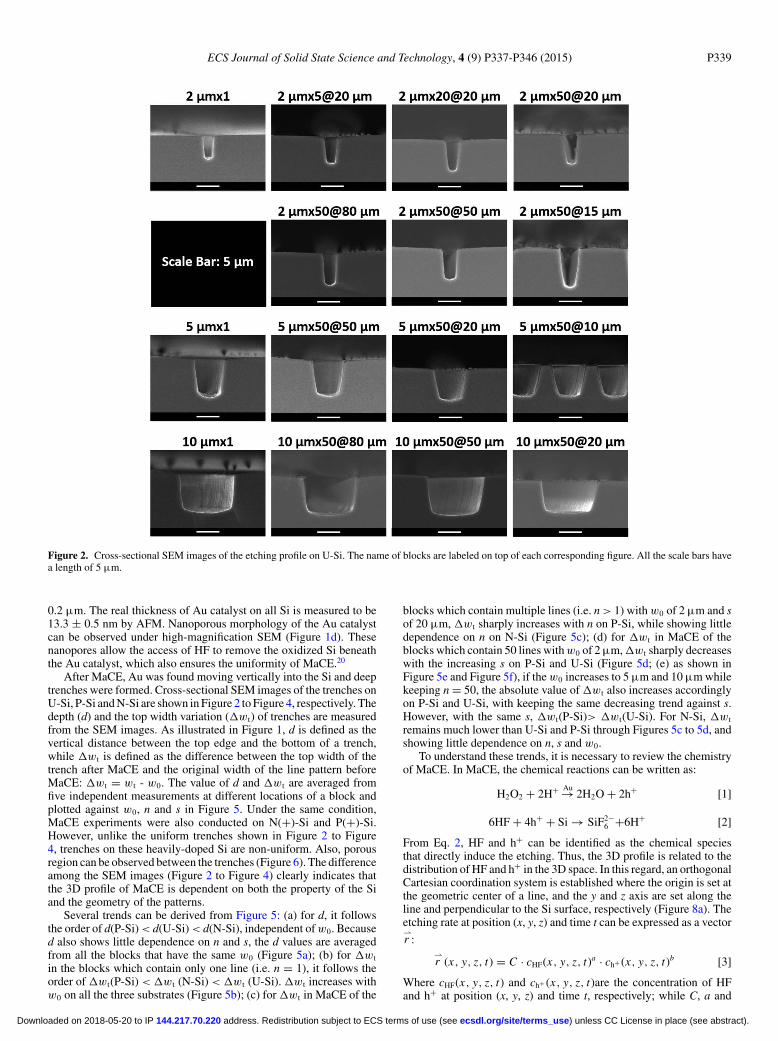
Figure 2. Cross-sectional SEM images of the etching profile on U-Si. The name of blocks are labeled on top of each corresponding figure. All the scale bars havea length of 5 μm.
0.2 μm. The real thickness of Au catalyst on all Si is measured to be13.3 ± 0.5 nm by AFM. Nanoporous morphology of the Au catalystcan be observed under high-magnification SEM (Figure 1d). Thesenanopores allow the access of HF to remove the oxidized Si beneaththe Au catalyst, which also ensures the uniformity of MaCE.20
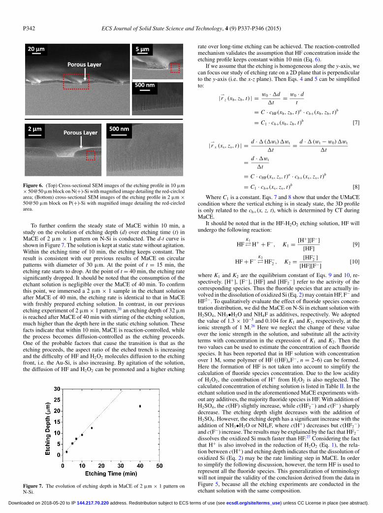
After MaCE, Au was found moving vertically into the Si and deeptrenches were formed. Cross-sectional SEM images of the trenches onU-Si, P-Si and N-Si are shown in Figure 2 to Figure 4, respectively. Thedepth (d) and the top width variation (�wt) of trenches are measuredfrom the SEM images. As illustrated in Figure 1, d is defined as thevertical distance between the top edge and the bottom of a trench,while �wt is defined as the difference between the top width of thetrench after MaCE and the original width of the line pattern beforeMaCE: �wt = wt - w0. The value of d and �wt are averaged fromfive independent measurements at different locations of a block andplotted against w0, n and s in Figure 5. Under the same condition,MaCE experiments were also conducted on N(+)-Si and P(+)-Si.However, unlike the uniform trenches shown in Figure 2 to Figure4, trenches on these heavily-doped Si are non-uniform. Also, porousregion can be observed between the trenches (Figure 6). The differenceamong the SEM images (Figure 2 to Figure 4) clearly indicates thatthe 3D profile of MaCE is dependent on both the property of the Siand the geometry of the patterns.
Several trends can be derived from Figure 5: (a) for d, it followsthe order of d(P-Si) < d(U-Si) < d(N-Si), independent of w0. Becaused also shows little dependence on n and s, the d values are averagedfrom all the blocks that have the same w0 (Figure 5a); (b) for �wt
in the blocks which contain only one line (i.e. n = 1), it follows theorder of �wt(P-Si) < �wt (N-Si) < �wt (U-Si). �wt increases withw0 on all the three substrates (Figure 5b); (c) for �wt in MaCE of the
blocks which contain multiple lines (i.e. n > 1) with w0 of 2 μm and sof 20 μm, �wt sharply increases with n on P-Si, while showing littledependence on n on N-Si (Figure 5c); (d) for �wt in MaCE of theblocks which contain 50 lines with w0 of 2 μm, �wt sharply decreaseswith the increasing s on P-Si and U-Si (Figure 5d; (e) as shown inFigure 5e and Figure 5f), if the w0 increases to 5 μm and 10 μm whilekeeping n = 50, the absolute value of �wt also increases accordinglyon P-Si and U-Si, with keeping the same decreasing trend against s.However, with the same s, �wt(P-Si)> �wt(U-Si). For N-Si, �wt
remains much lower than U-Si and P-Si through Figures 5c to 5d, andshowing little dependence on n, s and w0.
To understand these trends, it is necessary to review the chemistryof MaCE. In MaCE, the chemical reactions can be written as:
H2O2 + 2H+ Au→ 2H2O + 2h+ [1]
6HF + 4h+ + Si → SiF2−6 +6H+ [2]
From Eq. 2, HF and h+ can be identified as the chemical speciesthat directly induce the etching. Thus, the 3D profile is related to thedistribution of HF and h+ in the 3D space. In this regard, an orthogonalCartesian coordination system is established where the origin is set atthe geometric center of a line, and the y and z axis are set along theline and perpendicular to the Si surface, respectively (Figure 8a). Theetching rate at position (x, y, z) and time t can be expressed as a vector⇀r :
⇀r (x, y, z, t) = C · cHF(x, y, z, t)a · ch+ (x, y, z, t)b [3]
Where cHF(x, y, z, t) and ch+ (x, y, z, t)are the concentration of HFand h+ at position (x, y, z) and time t, respectively; while C, a and
) unless CC License in place (see abstract). ecsdl.org/site/terms_use address. Redistribution subject to ECS terms of use (see 144.217.70.220Downloaded on 2018-05-20 to IP
P340 ECS Journal of Solid State Science and Technology, 4 (9) P337-P346 (2015)
Figure 3. Cross-sectional SEM images of the etch-ing profile on P-Si. The name of blocks are labeled ontop of each corresponding figure. All the scale barshave a length of 5 μm.
Figure 4. Cross-sectional SEM images of the etch-ing profile on N-Si. The name of blocks are labeledon top of each corresponding figure. All the scale barshave a length of 5 μm.
) unless CC License in place (see abstract). ecsdl.org/site/terms_use address. Redistribution subject to ECS terms of use (see 144.217.70.220Downloaded on 2018-05-20 to IP
ECS Journal of Solid State Science and Technology, 4 (9) P337-P346 (2015) P341
Figure 5. (a) Plot of the average etching depth (d) versus original width of the line patterns (w0); (b) plot of the top width variation (�wt) versus w0 of thesingle-line patterns; (c) plot of the top width variation (�wt) versus number of line patterns (n) with w0 of 2 μm and spacing distance (s) of 20 μm; (d) plot of thetop width variation (�wt) versus s with w0 of 2 μm and n of 50; (e) plot of the top width variation (�wt) versus s with w0 of 5 μm and n of 50; (f) plot of the topwidth variation (�wt) versus s with w0 of 10 μm and n of 50. All the w0 here refer to the designed value. The solid lines in (b)-(f) represent the �wt calculatedfrom the diffusion model (labeled as P(M) and U(M) for P-Si and U-Si in the legend of each figure).
b are constants to be determined. The vector⇀r h+ is the unit vector
that points to the direction of the h+ movement. We further set the
start time of MaCE as t = 0. At t = 0,⇀r |(x, y, z, 0)| = 0. Since
�wt is larger than 0 in all the etching results, the trenches width afteretching is always larger than w0. The increase in w during MaCEindicates that the Si both beneath the Au catalysts and on the sidewallare etched. We refer to these two etching processes as the verticaletching and sidewall etching. Conceivably, d and �wt can be relatedto the reaction rate of vertical etching and sidewall etching, i.e. the
Where w, l and d are the dimension along x, y and z axis, V is volume ofSi being etched, while �d, �w and �V are the infinitesimal increasein d, w and V within the infinitesimal time period �t. (xb, yb, zb) and(xs, ys, zs)refer to the arbitrary positions at the bottom of the etchingprofiles (i.e. the Au-Si interface) and on the sidewall, respectively.
It has been demonstrated that under current UMaCE condition, |⇀r z |is constant within 10 min.20 Then we can assume that the verticaletching is under a steady state: cHF(x, y, z, t) and ch+ (x, y, z, t) inEq. 5 are constant over time. For HF, since the initial concentration ofHF equals to that in bulk solution, then:
cHF (x, y, z, t) = cHF (x, y, z, 0) = 1.5 mol/L [6]
Eq. 6 means that during the MaCE within 10 min, although theAu catalyst keeps moving into Si substrate, the etchant solution canquickly flow into the etched space above Au and a steady state isestablished within every infinitesimal time period, so that the localconcentration of HF at the Au –Si interface maintains the constantvalue. It is conceivable that the cHF(x, y, z, t) in Eq. 5 also equals tocHF(x, y, z, 0), since the sidewall and Au-Si are subjected to the sameetchant solution.
) unless CC License in place (see abstract). ecsdl.org/site/terms_use address. Redistribution subject to ECS terms of use (see 144.217.70.220Downloaded on 2018-05-20 to IP
P342 ECS Journal of Solid State Science and Technology, 4 (9) P337-P346 (2015)
Figure 6. (Top) Cross-sectional SEM images of the etching profile in 10 μm× 50@50 μm block on N(+)-Si with magnified image detailing the red-circledarea; (Bottom) cross-sectional SEM images of the etching profile in 2 μm ×50@50 μm block on P(+)-Si with magnified image detailing the red-circledarea.
To further confirm the steady state of MaCE within 10 min, astudy on the evolution of etching depth (d) over etching time (t) inMaCE of 2 μm × 1 pattern on N-Si is conducted. The d-t curve isshown in Figure 7. The solution is kept at static state without agitation.Within the etching time of 10 min, the etching keeps constant. Theresult is consistent with our previous results of MaCE on circularpatterns with diameter of 30 μm. At the point of t = 15 min, theetching rate starts to drop. At the point of t = 40 min, the etching ratesignificantly dropped. It should be noted that the consumption of theetchant solution is negligible over the MaCE of 40 min. To confirmthis point, we immersed a 2 μm × 1 sample in the etchant solutionafter MaCE of 40 min, the etching rate is identical to that in MaCEwith freshly prepared etching solution. In contrast, in our previousetching experiment of 2 μm × 1 pattern,20 an etching depth of 32 μmis reached after MaCE of 40 min with stirring of the etching solution,much higher than the depth here in the static etching solution. Thesefacts indicate that within 10 min, MaCE is reaction-controlled, whilethe process becomes diffusion-controlled as the etching proceeds.One of the probable factors that cause the transition is that as theetching proceeds, the aspect ratio of the etched trench is increasingand the difficulty of HF and H2O2 molecules diffusion to the etchingfront, i.e. the Au-Si, is also increasing. By agitation of the solution,the diffusion of HF and H2O2 can be promoted and a higher etching
Figure 7. The evolution of etching depth in MaCE of 2 μm × 1 pattern onN-Si.
rate over long-time etching can be achieved. The reaction-controlledmechanism validates the assumption that HF concentration inside theetching profile keeps constant within 10 min (Eq. 6).
If we assume that the etching is homogeneous along the y-axis, wecan focus our study of etching rate on a 2D plane that is perpendicularto the y-axis (i.e. the x-z plane). Then Eqs. 4 and 5 can be simplifiedto:
|⇀r z (xb, zb, t) | = w0 · �d
�t= w0 · d
t
= C · cHF(xb, zb, t)a · ch+(xb, zb, t)b
= C1 · ch+(xb, zb, t)b [7]
|⇀r x (xs, zs, t) | = d · � (�wt) �wt
�t= d · � (wt − w0) �wt
�t
= d · �wt
�t
= C · cHF(xs, zs, t)a · ch+(xs, zs, t)b
= C1 · ch+(xs, zs, t)b [8]
Where C1 is a constant. Eqs. 7 and 8 show that under the UMaCEcondition where the vertical etching is in steady state, the 3D profileis only related to the ch+(x, z, t), which is determined by CT duringMaCE.
It should be noted that in the HF-H2O2 etching solution, HF willundergo the following reaction:
HFK1
� H+ + F−, K1 = [H+][F−]
[HF][9]
HF + F− K2
� HF−2 , K2 = [HF−
2 ]
[HF][F−][10]
where K1 and K2 are the equilibrium constant of Eqs. 9 and 10, re-spectively. [H+], [F−], [HF] and [HF2
−] refer to the activity of thecorresponding species. Thus the fluoride species that are actually in-volved in the dissolution of oxidized Si (Eq. 2) may contain HF, F− andHF2−. To qualitatively evaluate the effect of fluoride species concen-tration distribution, we did the MaCE on N-Si in etchant solution withH2SO4, NH3•H2O and NH4F as additives, respectively. We adoptedthe value of 1.3 × 10⁻³ and 0.104 for K1 and K2, respectively, at theionic strength of 1 M.26 Here we neglect the change of these valueover the ionic strength in the solution, and substitute all the activityterms with concentration in the expression of K1 and K2. Then thetwo values can be used to estimate the concentration of each fluoridespecies. It has been reported that in HF solution with concentrationover 1 M, some polymer of HF ((HF)nF−, n = 2–6) can be formed.Here the formation of HF is not taken into account to simplify thecalculation of fluoride species concentration. Due to the low acidityof H2O2, the contribution of H+ from H2O2 is also neglected. Thecalculated concentration of etching solution is listed in Table II. In theetchant solution used in the aforementioned MaCE experiments with-out any additives, the majority fluoride species is HF. With addition ofH2SO4, the c(HF) slightly increase, while c(HF2
−) and c(F−) sharplydecrease. The etching depth slight decreases with the addition ofH2SO4. However, the etching depth has a significant increase with theaddition of NH3•H2O or NH4F, where c(H+) decreases but c(HF2
−)and c(F−) increase. The results may be explained by the fact that HF2
−
dissolves the oxidized Si much faster than HF.27 Considering the factthat H+ is also involved in the reduction of H2O2 (Eq. 1), the rela-tion between c(H+) and etching depth indicates that the dissolution ofoxidized Si (Eq. 2) may be the rate limiting step in MaCE. In orderto simplify the following discussion, however, the term HF is used torepresent all the fluoride species. This generalization of terminologywill not impair the validity of the conclusion derived from the data inFigure 5, because all the etching experiments are conducted in theetchant solution with the same composition.
) unless CC License in place (see abstract). ecsdl.org/site/terms_use address. Redistribution subject to ECS terms of use (see 144.217.70.220Downloaded on 2018-05-20 to IP
aThe concentration of additive molecules. For H2SO4 as the additive, the pKa2 for the second proton dissociation is 1.99, ∼10 times higher than pKa ofHF, thus it is assumed that the H2SO4 molecules completely dissociate and provide two protons per molecules; for NH3•H2O as the additive, the pKb ofNH3•H2O is 4.75, it is assumed that all the NH3•H2O molecules is bonded with protons in the solution; for NH4F as the additives, it is assumed that allNH4F dissociate into NH4
+ and F− ions. The pKa and pKb values mentioned above can be found in Ref. 37;bDepth of etching profile averaged from 5 independent tests on N-Si under the same condition as those used in Figs. 2–4;cStandard deviation of etching depth in μm.
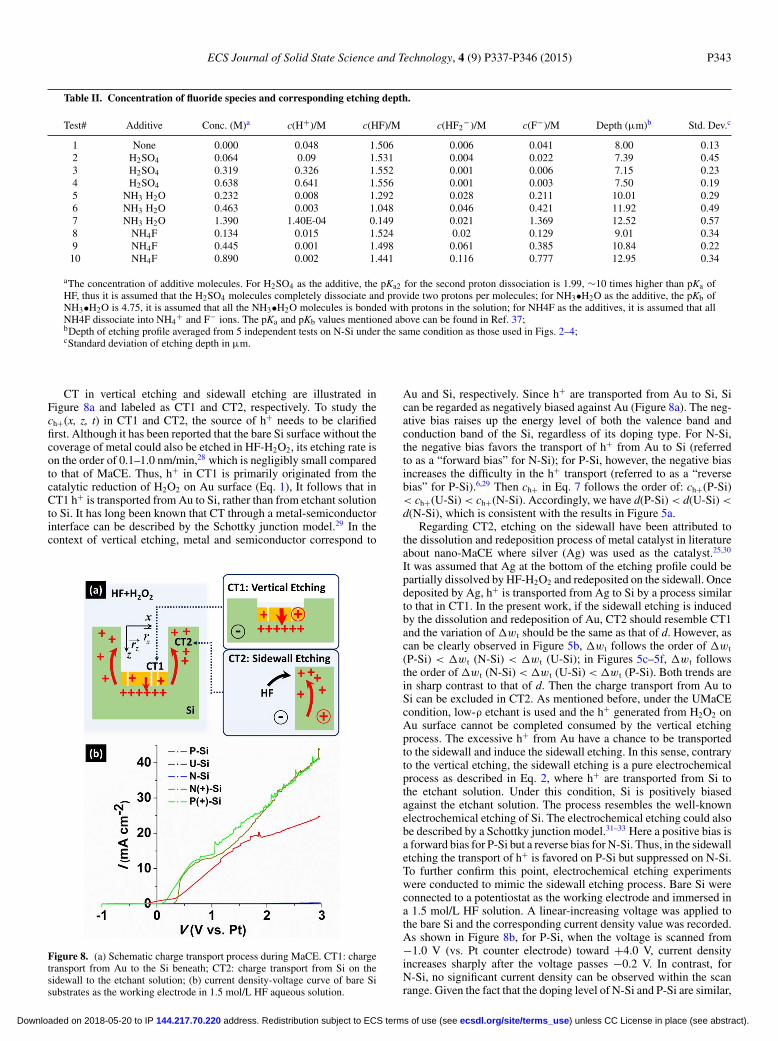
CT in vertical etching and sidewall etching are illustrated inFigure 8a and labeled as CT1 and CT2, respectively. To study thech+(x, z, t) in CT1 and CT2, the source of h+ needs to be clarifiedfirst. Although it has been reported that the bare Si surface without thecoverage of metal could also be etched in HF-H2O2, its etching rate ison the order of 0.1–1.0 nm/min,28 which is negligibly small comparedto that of MaCE. Thus, h+ in CT1 is primarily originated from thecatalytic reduction of H2O2 on Au surface (Eq. 1), It follows that inCT1 h+ is transported from Au to Si, rather than from etchant solutionto Si. It has long been known that CT through a metal-semiconductorinterface can be described by the Schottky junction model.29 In thecontext of vertical etching, metal and semiconductor correspond to
Figure 8. (a) Schematic charge transport process during MaCE. CT1: chargetransport from Au to the Si beneath; CT2: charge transport from Si on thesidewall to the etchant solution; (b) current density-voltage curve of bare Sisubstrates as the working electrode in 1.5 mol/L HF aqueous solution.
Au and Si, respectively. Since h+ are transported from Au to Si, Sican be regarded as negatively biased against Au (Figure 8a). The neg-ative bias raises up the energy level of both the valence band andconduction band of the Si, regardless of its doping type. For N-Si,the negative bias favors the transport of h+ from Au to Si (referredto as a “forward bias” for N-Si); for P-Si, however, the negative biasincreases the difficulty in the h+ transport (referred to as a “reversebias” for P-Si).6,29 Then ch+ in Eq. 7 follows the order of: ch+(P-Si)< ch+(U-Si) < ch+(N-Si). Accordingly, we have d(P-Si) < d(U-Si) <d(N-Si), which is consistent with the results in Figure 5a.
Regarding CT2, etching on the sidewall have been attributed tothe dissolution and redeposition process of metal catalyst in literatureabout nano-MaCE where silver (Ag) was used as the catalyst.25,30
It was assumed that Ag at the bottom of the etching profile could bepartially dissolved by HF-H2O2 and redeposited on the sidewall. Oncedeposited by Ag, h+ is transported from Ag to Si by a process similarto that in CT1. In the present work, if the sidewall etching is inducedby the dissolution and redeposition of Au, CT2 should resemble CT1and the variation of �wt should be the same as that of d. However, ascan be clearly observed in Figure 5b, �wt follows the order of �wt
(P-Si) < �wt (N-Si) < �wt (U-Si); in Figures 5c–5f, �wt followsthe order of �wt (N-Si) < �wt (U-Si) < �wt (P-Si). Both trends arein sharp contrast to that of d. Then the charge transport from Au toSi can be excluded in CT2. As mentioned before, under the UMaCEcondition, low-ρ etchant is used and the h+ generated from H2O2 onAu surface cannot be completed consumed by the vertical etchingprocess. The excessive h+ from Au have a chance to be transportedto the sidewall and induce the sidewall etching. In this sense, contraryto the vertical etching, the sidewall etching is a pure electrochemicalprocess as described in Eq. 2, where h+ are transported from Si tothe etchant solution. Under this condition, Si is positively biasedagainst the etchant solution. The process resembles the well-knownelectrochemical etching of Si. The electrochemical etching could alsobe described by a Schottky junction model.31–33 Here a positive bias isa forward bias for P-Si but a reverse bias for N-Si. Thus, in the sidewalletching the transport of h+ is favored on P-Si but suppressed on N-Si.To further confirm this point, electrochemical etching experimentswere conducted to mimic the sidewall etching process. Bare Si wereconnected to a potentiostat as the working electrode and immersed ina 1.5 mol/L HF solution. A linear-increasing voltage was applied tothe bare Si and the corresponding current density value was recorded.As shown in Figure 8b, for P-Si, when the voltage is scanned from−1.0 V (vs. Pt counter electrode) toward +4.0 V, current densityincreases sharply after the voltage passes −0.2 V. In contrast, forN-Si, no significant current density can be observed within the scanrange. Given the fact that the doping level of N-Si and P-Si are similar,
) unless CC License in place (see abstract). ecsdl.org/site/terms_use address. Redistribution subject to ECS terms of use (see 144.217.70.220Downloaded on 2018-05-20 to IP
P344 ECS Journal of Solid State Science and Technology, 4 (9) P337-P346 (2015)
Figure 9. Calculated ch+(x,0,10 min) in MaCE of 2 μm × 1, 5 μm × 1 and 10 μm × 1 blocks using diffusion model. (a) and (b) show the overall curve andmagnified curve of the near-Au edge part, respectively. In (b), the origin of x-axis is set at the boundary between the edge of Au and Si indicated by the verticallines in (a). The horizontal line in both (a) and (b) is the line of ch+ = ch+crit = 0.1645.
the result supports the point that once a positive bias is applied, h+
can be favorably transported from P-Si to HF solution, while h+
transport from N-Si to HF solution is intrinsically suppressed. It isobserved that the current density of U-Si is also low, which maybe attributed to the low doping level of U-Si (Table I). For P(+)and N(+)-Si, however, due to a high doping level, h+ can easilytunnel through the Si-HF solution interface regardless of the dopanttype, thus their current density increases faster than P-Si.29 DuringMaCE of the heavily doped Si, the tunneling process not only inducessidewall etching, but also makes the Si between trenches highly porouson both substrates (Figure 6), which is consistent with results fromprevious results of electrochemical etching34 and nano-MaCE35–37
on heavily-doped Si.Now that CT1 and CT2 have been discussed, we can further inves-
tigate the correlation between CT1 and CT2. As discussed above,h+ in both CT1 and CT2 are originated from the reduction ofH2O2 on Au surface. Under the steady state, ch+ in CT1 is con-stant over time, which means Au can be regarded as a source thatconstantly emits h+ into Si while moving along the z-axis at constantvelocity (v):
ch+ (x, z, t) = ch+ (x, z, 0) = constant
= ch+ECTH (x, z, t) + ch+EX (x, z, t) [11]
where ch+ETCH(x, z, t) is the amount of h+ that are consumed in thevertical etching, while ch+EX(x, z, t) is the amount of excessive h+.Since the vertical etching rate is constant, then ch+ETCH(x, z, t) isconstant, which makes ch+EX(x, z, t) also constant:
ch+EX (x, z, t) = ch+EX = constant [12]
These excessive h+ can be transported to the sidewall throughdiffusion or drift. Here the term “diffusion” refers to the movementof h+ driven by the gradient of ch+, while “drift” refers to that drivenby electric field. If we assume that the excessive h+ is the only sourceof h+ in CT2 and transported to the sidewall only through diffusion,then we can establish a diffusion model to calculate ch+ in Eq. 8 byFick’s Second Law:
∂ch+ (x, z, t)
∂t= D∇2ch+ (x, z, t) [13]
where D is the diffusion constant of h+ in Si. Here D is set as constantover space and time. If we introduce a new variable r = √
x2 + z2,the boundary condition and initial condition can be written as:
∂ch+ (r, t)
∂r
∣∣√r=vt = ch+EX (r, t) δ (t) [14]
ch+ (r, t) |r→∞ = 0 [15]
ch+ (x, z, 0) = 0 [16]
Assuming the total ch+ is the sum of the contribution of each Aulines in a w0 × n@s block, we have:38
ch+ (x, z, t) =n∑
ni =1
( ∫ w0/2
−w0/2dw
∫ t
0
ch+EX
4πD (t − τ)
× exp
(− (x − w − ni × s)2 + (z − vτ)2
4D (t − τ)
)dτ
)
[17]
It has been reported that in the electrochemical etching process, Si iscompletely removed when ch+ exceeds a certain critical value ch+crit,while porous Si is formed when ch+ is below ch+crit.31 Then using thediffusion model, �wt can be calculated by Eq. 17 if we assume that�wt is only related to the ch+ on the Si top surface at z = 0 (referredto as ch+(x, 0, 10 min)). The ch+(x, 0, 10 min) equals to ch+crit atthe position of (�wt, 0). Figure 9a shows the calculated ch+(x, 0, 10min) in MaCE of 2 μm × 1, 5 μm × 5, 10 μm × 1 blocks on U-Sialong x-axis where the origin is set at the geometric center of Aulines. The ch+ is calculated by fitting Eq. 17 with �wt in Figure 5band expressed in arbitrary unit (a.u.). The fitting gives nominal valueof ch+crit = 0.164 and D = 0.008 μm2/s. The boundaries betweenthe edge of Au and Si are indicated as the vertical dot lines at x =±w0/2. For example, the boundaries of 2 μm × 1 block locate at x= ±1 μm. As the w0 increases, ch+ within the boundary increasesand the curve extends farther out of the boundary, which is consistentwith results in Figure 5b. To calculate �wt, the ch+ curve outside theboundaries is detailed in Figure 9b, where the x-axis is set to startat the boundary of Au in each curve of Figure 9a and extend out ofthe boundary. Then the curves in Figure 9b represent the ch+ in thesidewall, which is involved in CT2. Given ch+crit = 0.164, �wt of eachcurve in Figure 5 can be identified by locating the intersection point ofthe curves with the ch+ = 0.164 line (horizontal black dash line). Wename these �wt value as the modeled value. The modeled �wt for P-Si and U-Si are plotted in Figure 5b as solid lines and labeled as P(M)and U(M), which shows good consistence with the experimentallymeasured value. The same ch+crit and D value are used to obtain themodeled �wt in MaCE of other blocks, which are plotted in Figure 5cto 5e. For U-Si, the modeled �wt are close to the measured value. ForP-Si, ch+crit and D are fit to be 0.340 and 0.003 μm2/s from Figure 5b.However, although the modeled �wt well match the measured valueFigure 5b, they are far below the measured value in Figures 5c to 5e.The comparison between the modeled and measured �wt in Figure 5bto 5e indicates that for U-Si, h+ transported from Au to the sidewall islikely to be a diffusion process mainly from the excessive h+ aroundAu. For P-Si, in single line etching, h+ is also transported from Authrough diffusion; in multiple line etching, however, the actual h+
concentration in the sidewall region is much higher than the amount
) unless CC License in place (see abstract). ecsdl.org/site/terms_use address. Redistribution subject to ECS terms of use (see 144.217.70.220Downloaded on 2018-05-20 to IP
ECS Journal of Solid State Science and Technology, 4 (9) P337-P346 (2015) P345
Figure 10. Cross-sectional SEM images of the etching profile on P-Si with (111) crystalline orientation. The name of blocks are labeled on top of eachcorresponding figure. All the scale bars have a length of 5 μm.
that transported through diffusion. The sharp increase of �wt with non P-Si has not been reported before. Considering the fact that a largeamount of h+ is transported from Au to Si, a strong electric field maybe established around every Au lines. Based on the depth of etchingas ∼6 μm on P-Si, the amount of Si etched per unit area rz in theetching of 10 min is:
rz = ρV
MSit= 6 μm × 1 μm × 1 μm × 2.329 g/cm3
28.09 g/mol × 600 s
= 8.3 × 10⁻¹⁶ mol/s [18]
Where ρ, V, MSi are the density, etched volume and molecular weightof Si.39 Assuming etching of each Si atom consumes 4 h+, then thecurrent density of h+ is estimated to be:
According to Figure 8b, the current correspond to a bias over 3 V.In MaCE of multiple Au lines, the increase of n may significantlyincrease the synergistic electric field from all Au lines, which resultedin an increased amount of intrinsic h+ that are involved in CT2 andan accelerated movement of h+ toward sidewall. Besides, in P-Si, aconsiderable amount of h+ exist at the dopant atoms in Si as intrinsich+. These h+ also have a chance to be transported to the sidewallunder the electric field. Therefore, although in the single Au lineetching, �wt (U-Si) is larger than �wt (P-Si) due to a higher amountof excessive h+ in CT1 (Figure 5b), �wt (P-Si) quickly exceeds�wt (U-Si) as n increases (Figures 5c–5e). However, further study isneeded to figure out the spatial distribution of the electric field and itsinteraction with h+ inside Si.
In order to investigate the MaCE results on Si with other crystallineorientation, we conducted MaCE on the P-Si with (111)-orientationunder the same condition as that on P-Si with (100)-orientation. Asshown in Figure 10, after MaCE vertical trenches were formed onthe (111)-Si substrates, in consistence with previous results.21 Similarto the results from (100)-Si, here the �wt also shows an increasewhen n increases. The increase of �wt support the aforementionedmechanism that the charge transport during MaCE can be described bythe Schottky models, where the doping of the Si plays the major role.The etching depth is much lower than that on (100)-Si. The sloweretching rate on (111)-Si may be explained by the fact that the backbonds density is higher along the 〈111〉 orientation than that along〈100〉 orientation.
Conclusions
In conclusion, 3D profiles of MaCE using Au lines with differentline width (w0), number (n) and spacing distance (s) on P-Si, N-Si,USi, P(+)-Si and N(+)-Si have been presented. Uniform trencheswere formed on P-Si, N-Si and U-Si, while the 3D profiles on P(+)-Siand N(+)-Si are non-uniform. The depth d and lateral width variation�wt of the 3D profiles on P-Si, N-Si and U-Si are measured and
correlated to the CT1 and CT2, respectively. The depth follows theorder of d(P-Si) < d(U-Si) < d(N-Si),while the �wt of N-Si is lowerthan that of U-Si and P-Si. The variation of d and �wt over thedopant type of Si can be explained by Schottky junction model, whichindicates that CT1 is favored on N-Si and CT2 is favored on P-Si.The variation of �wt over w0, n and s can be further explained bythe correlation between CT1 and CT2: in U-Si, h+ in CT2 are mainlyoriginated from excessive h+ in CT1 through diffusion; in P-Si, theactual h+ concentration in CT2 is much higher than that calculatedfrom the diffusion model, which may be attributed to the drift of h+.
The fundamental aspects revealed by the present work will serveas a reference for future MaCE research. It is expected that by deeperstudy about the effect of electric bias, etchant composition and otherparameters, a complete controllability of 3D profiles in MaCE canbe achieved. The novel insight is also meaningful in general electro-chemistry where charge transport process in micro- and nanoscale areconcerned, such as microfluidics and MEMS. Practically, the resultspave the way to the fabrication of high-density micro- and nanostruc-tures by MaCE: vertical HAR structures can be readily formed onN-Si; the sidewall of the etched structures will be tapered on P-Si andU-Si as the pattern number and density increase, where the effect oflateral geometry of the structures should also be considered.
Acknowledgment
The authors thank National Science Foundation (CMMI 1130876)for funding support. L. L. did the experiments and data collection/analysis. X. Z. did modeling of h+ distribution. All the authors con-tribute to the composition of the manuscripts.
References
1. F. Ayazi and K. Najafi, J. Microelectromech. Syst., 9, 288 (2000).2. M. W. Newman, S. Muthukumar, M. Schuelein, T. Dambrauskas, P. A. Dunaway,
J. M. Jordan, S. Kulkarni, C. D. Linde, T. A. Opheim, R. A. Stingel, W. Worwag,L. A. Topic, and J. M. Swan, in Electronic Components and Technology Conference,2006. Proceedings. 56th, p. 5 (2006).
3. C. Chang, Y.-F. Wang, Y. Kanamori, J.-J. Shih, Y. Kawai, C.-K. Lee, K.-C. Wu, andM. Esashi, J. Micromech. Microeng., 15, 580 (2005).
4. H. Jansen, M. Deboer, R. Legtenberg, and M. Elwenspoek, J. Micromech. Microeng.,5, 115 (1995).
5. X. Li and P. W. Bohn, Appl. Phys. Lett., 77, 2572 (2000).6. Z. Huang, N. Geyer, P. Werner, J. de Boor, and U. Gosele, Adv. Mater., 23, 285
(2011).7. L. Li and C. P. Wong, in Electronic Components and Technology Conference (ECTC),
2013 IEEE 63rd, p. 2326 (2013).8. X. Li, Curr. Opin. Solid State Mater. Sci., 16, 71 (2012).9. K. Peng, Y. Xu, Y. Wu, Y. Yan, S.-T. Lee, and J. Zhu, Small, 1, 1062 (2005).
10. K. Q. Peng, Y. J. Yan, S. P. Gao, and J. Zhu, Adv. Mater., 14, 1164 (2002).11. Z. Huang, X. Zhang, M. Reiche, L. Liu, W. Lee, T. Shimizu, S. Senz, and U. Gosele,
Nano Lett., 8, 3046 (2008).12. J. Kim, Y. H. Kim, S.-H. Choi, and W. Lee, ACS Nano, 5, 5242 (2011).13. J. Kim, H. Han, Y. H. Kim, S.-H. Choi, J.-C. Kim, and W. Lee, ACS Nano, 5, 3222
(2011).14. S. W. Chang, V. P. Chuang, S. T. Boles, and C. V. Thompson, Adv. Funct. Mater., 20,
4364 (2010).15. Z. Huang, T. Shimizu, S. Senz, Z. Zhang, N. Geyer, and U. Gosele, J. Phys. Chem.
C, 114, 10683 (2010).16. R. G. Milazzo, G. D’Arrigo, C. Spinella, M. G. Grimaldi, and E. Rimini, J Elec-
trochem Soc, 159, D521 (2012).17. C. Chang and A. Sakdinawat, Nat. Commun., 5 (2014).18. Y. Liu, A. Das, Z. Lin, I. B. Cooper, A. Rohatgi, and C. P. Wong, Nano Energy, 3,
127 (2014).
) unless CC License in place (see abstract). ecsdl.org/site/terms_use address. Redistribution subject to ECS terms of use (see 144.217.70.220Downloaded on 2018-05-20 to IP
P346 ECS Journal of Solid State Science and Technology, 4 (9) P337-P346 (2015)
19. Z. Mohammad, F. Saeed Delaram, K. Mahdi, M. Hamed, E. Alireza, and Z. Firooz,J. Micromech. Microeng., 23, 055015 (2013).
20. L. Li, Y. Liu, X. Zhao, Z. Lin, and C.-P. Wong, ACS Appl. Mater. Interfaces, 6, 575(2014).
21. L. Li, X. Zhao, and C.-P. Wong, ACS Appl. Mater. Interfaces, 6, 16782 (2014).22. K. Booker, M. Brauers, E. Crisp, S. Rahman, K. Weber, M. Stocks, and A. Blakers,
J. Micromech. Microeng., 24, 125026 (2014).23. M. Sato and Y. Arita, J. Electrochem. Soc., 134, 2856 (1987).24. S. Li, W. Ma, Y. Zhou, X. Chen, Y. Xiao, M. Ma, W. Zhu, and F. Wei, Nanoscale
J. Phys. Chem. C, 112, 4444 (2008).26. H. Proksche, G. Nagorsen, and D. Ross, J. Electrochem. Soc, 139, 521
(1992).27. J. S. Judge, J. Electrochem. Soc, 118, 1772 (1971).28. C. Gondek, M. Lippold, I. Rover, K. Bohmhammel, and E. Kroke, J. Phys. Chem. C,
118, 2044 (2014).
29. S. M. Sze, Semiconductor Devices Physics and Technology, p. 225, John Wiley &Sons, Inc (2002).
30. X. Zhong, Y. Qu, Y.-C. Lin, L. Liao, and X. Duan, ACS Appl. Mater. Interfaces, 3,261 (2011).
31. V. Lehmann, Electrochemistry of Silicon, p. 77, WILEY-VCH Verlag GmBH, Wein-heim (2002).
32. V. Lehmann and H. Foll, J. Electrochem. Soc., 137, 653 (1990).33. V. Lehmann and U. Gosele, Appl. Phys. Lett., 58, 856 (1991).34. V. Lehmann, R. Stengl, and A. Luigart, Mater. Sci. Eng. B, 69–70, 11 (2000).35. W.-K. To, C.-H. Tsang, H.-H. Li, and Z. Huang, Nano Lett., 11, 5252 (2011).36. Y. Qi, Z. Wang, M. Zhang, F. Yang, and X. Wang, J. Phys. Chem. C, 117, 25090
(2013).37. K. Balasundaram, J. S. Sadhu, J. C. Shin, B. Azeredo, D. Chanda, M. Malik, K. Hsu,
J. A. Rogers, P. Ferreira, S. Sinha, and X. Li, Nanotechnology, 23, 305304 (2012).38. J. Taler and P. Duda, Solving Direct and Inverse Heat Conduction Problems, p. 765,
Springer-Verlag, Berlin (2006).39. CRC Handbook of Chemistry and Physics, p. 4, CRC Press (2004).
) unless CC License in place (see abstract). ecsdl.org/site/terms_use address. Redistribution subject to ECS terms of use (see 144.217.70.220Downloaded on 2018-05-20 to IP