34
Charged Device Model (CDM) Qualification Issues
Charged Device Model (CDM) Qualification Issues
Industry Council on ESD Target Levels CDM Presentation
2
Purpose /Abstract
• IC design for performance constraints make it increasingly difficult to meet the current CDM levels as the technologies continue to shrink and the circuit speed demands continue to increase
• This work shows that devices with CDM levels below the general target of 500 V can safely be handled with CDM control methods available in the industry today
• Based on these observations and constraints it will be shown through this work that 250V is a safe and practical target CDM level
Industry Council on ESD Target Levels CDM Presentation
3
Outline
• Relevance of CDM
• CDM Technology & Design Issues
• CDM Qualification Methods
• ESD Control Methods Addressing CDM
• Analysis of Field Return Data
• Summary
• Conclusion
• Roadmap
Industry Council on ESD Target Levels CDM Presentation
4
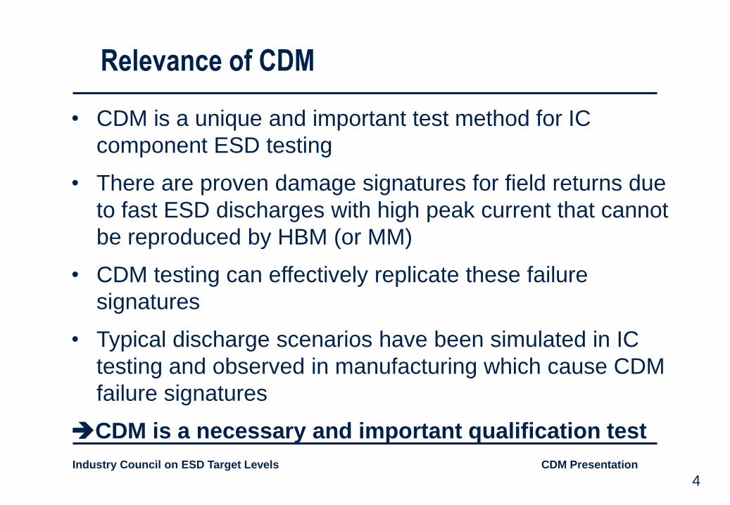
Relevance of CDM
• CDM is a unique and important test method for IC
component ESD testing
• There are proven damage signatures for field returns due
to fast ESD discharges with high peak current that cannot
be reproduced by HBM (or MM)
• CDM testing can effectively replicate these failure
signatures
• Typical discharge scenarios have been simulated in IC
testing and observed in manufacturing which cause CDM
failure signatures
CDM is a necessary and important qualification test
Industry Council on ESD Target Levels CDM Presentation
5
• CDM protection design is primarily driven by the peak
current from the IC package discharge at the required
(targeted) CDM voltage level.
• Increasing package size (and capacitance) lead to
increasing peak CDM current for a given CDM stress
voltage.
• Additionally, CDM protection design is increasingly limited
by reduction in breakdown voltage of gate dielectrics and
junctions.
CDM Technology & Design Issues
Industry Council on ESD Target Levels CDM Presentation
6
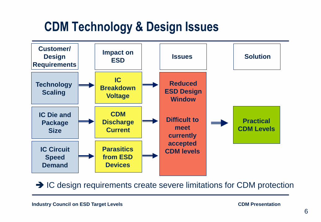
IC Circuit
Speed
Demand
IC Die and
Package
Size
Technology
Scaling
IC
Breakdown
Voltage
Reduced
ESD Design
Window
Practical
CDM Levels
CDM Technology & Design Issues
Parasitics
from ESD
Devices
IC design requirements create severe limitations for CDM protection
CDM
Discharge
Current
Customer/
Design
Requirements
Impact on
ESD Issues Solution
Difficult to
meet
currently
accepted
CDM levels
Industry Council on ESD Target Levels CDM Presentation
7
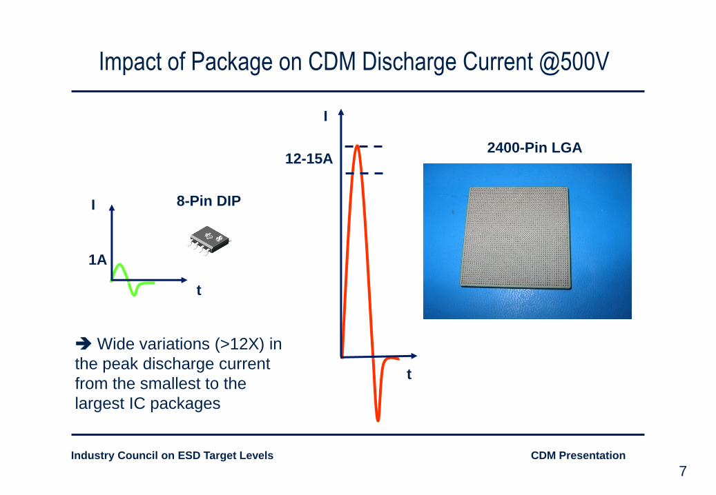
Impact of Package on CDM Discharge Current @500V
I
t
1A
I
t
12-15A
8-Pin DIP
2400-Pin LGA
Wide variations (>12X) in
the peak discharge current
from the smallest to the
largest IC packages
Industry Council on ESD Target Levels CDM Presentation
8
500
1000
1500
2000
2500
3000
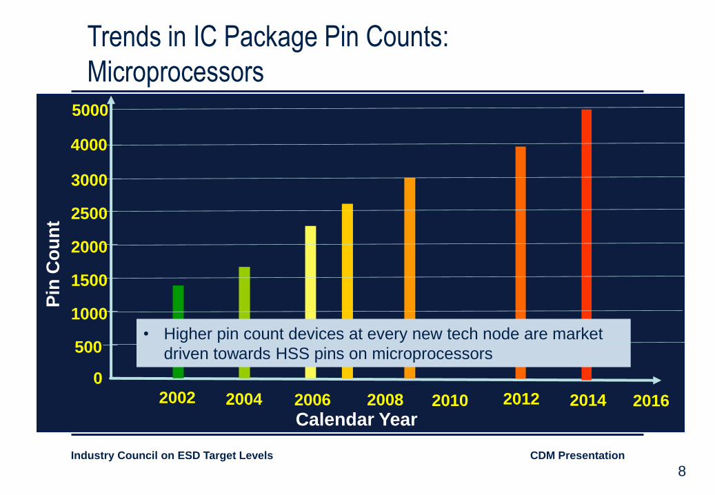
2002
0
Pin
Co
un
t
2004 2006 2008 2010
Calendar Year
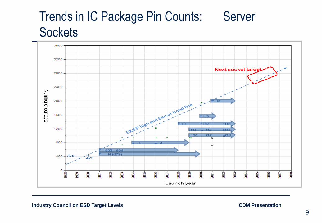
Trends in IC Package Pin Counts:
Microprocessors
2012 2014 2016
4000
5000
• Higher pin count devices at every new tech node are market
driven towards HSS pins on microprocessors
Industry Council on ESD Target Levels CDM Presentation
9
Calendar Year
370423
603 604
T J
B1 B2 B3
H1 H2 H3
G1 G2 G3
R
LS
N (479)
Num
ber of contacts
Launch year
Next socket target
Trends in IC Package Pin Counts: Server
Sockets
Industry Council on ESD Target Levels CDM Presentation
10
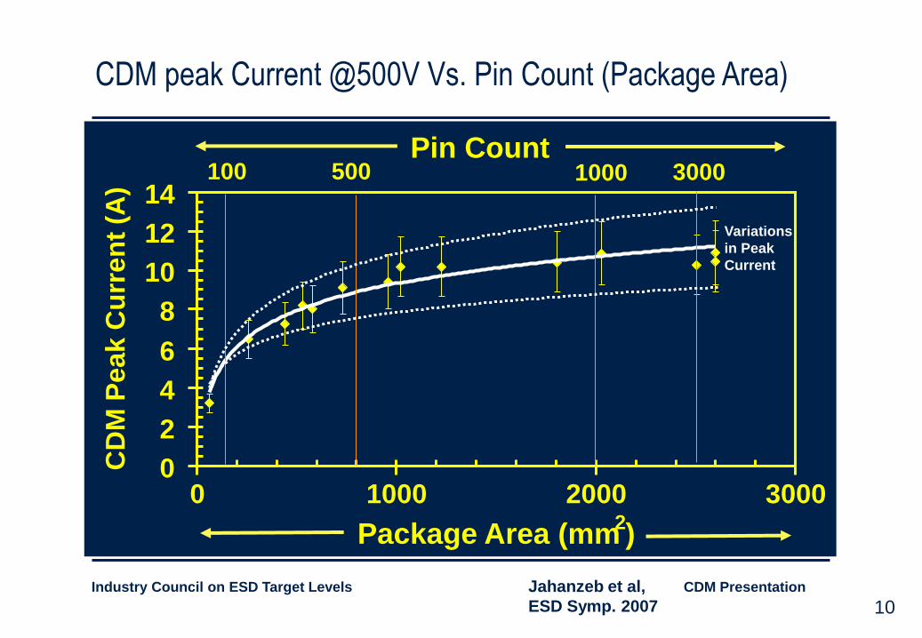
CDM peak Current @500V Vs. Pin Count (Package Area)
Jahanzeb et al,
ESD Symp. 2007
0
2
4
6
8
10
12
14
0 1000 2000 3000
Package Area (mm 2 )
CD
M P
ea
k C
urr
en
t (A
)
100 3000 1000 500 Pin Count
Variations
in Peak
Current
Industry Council on ESD Target Levels CDM Presentation
11
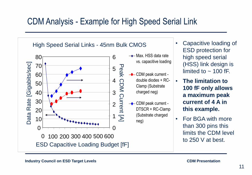
• Capacitive loading of
ESD protection for
high speed serial
(HSS) link design is
limited to ~ 100 fF.
• The limitation to
100 fF only allows
a maximum peak
current of 4 A in
this example.
• For BGA with more
than 300 pins this
limits the CDM level
to 250 V at best.
CDM Analysis - Example for High Speed Serial Link
High Speed Serial Links - 45nm Bulk CMOS
0
10
20
30
40
50
60
70
80
0 100 200 300 400 500 600
ESD Capacitive Loading Budget [fF]
Data
Rate
[G
igabits/s
ec]
0
1
2
3
4
5
6
Peak C
DM
Curre
nt [A
]
Max. HSS data rate
vs. capacitive loading
CDM peak current -
double diodes + RC-
Clamp (Substrate
charged neg)
CDM peak current -
DTSCR + RC-Clamp
(Substrate charged
neg)
Industry Council on ESD Target Levels CDM Presentation
12
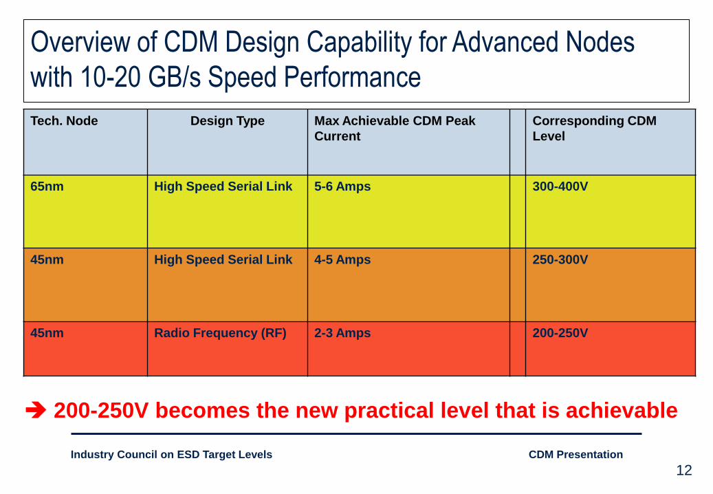
Overview of CDM Design Capability for Advanced Nodes
with 10-20 GB/s Speed Performance
Tech. Node Design Type Max Achievable CDM Peak
Current
Corresponding CDM
Level
65nm High Speed Serial Link 5-6 Amps 300-400V
45nm High Speed Serial Link 4-5 Amps 250-300V
45nm Radio Frequency (RF) 2-3 Amps 200-250V
200-250V becomes the new practical level that is achievable
Industry Council on ESD Target Levels CDM Presentation
13
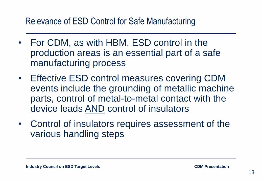
Relevance of ESD Control for Safe Manufacturing
• For CDM, as with HBM, ESD control in the production areas is an essential part of a safe manufacturing process
• Effective ESD control measures covering CDM events include the grounding of metallic machine parts, control of metal-to-metal contact with the device leads AND control of insulators
• Control of insulators requires assessment of the various handling steps
Industry Council on ESD Target Levels CDM Presentation
14
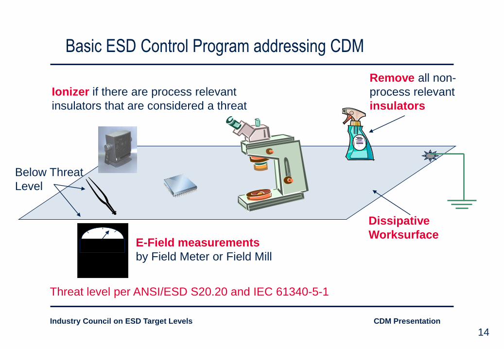
Basic ESD Control Program addressing CDM
Ionizer if there are process relevant
insulators that are considered a threat
Remove all non-
process relevant
insulators
E-Field measurements
by Field Meter or Field Mill
Below Threat
Level
Dissipative
Worksurface
Threat level per ANSI/ESD S20.20 and IEC 61340-5-1
Industry Council on ESD Target Levels CDM Presentation
15
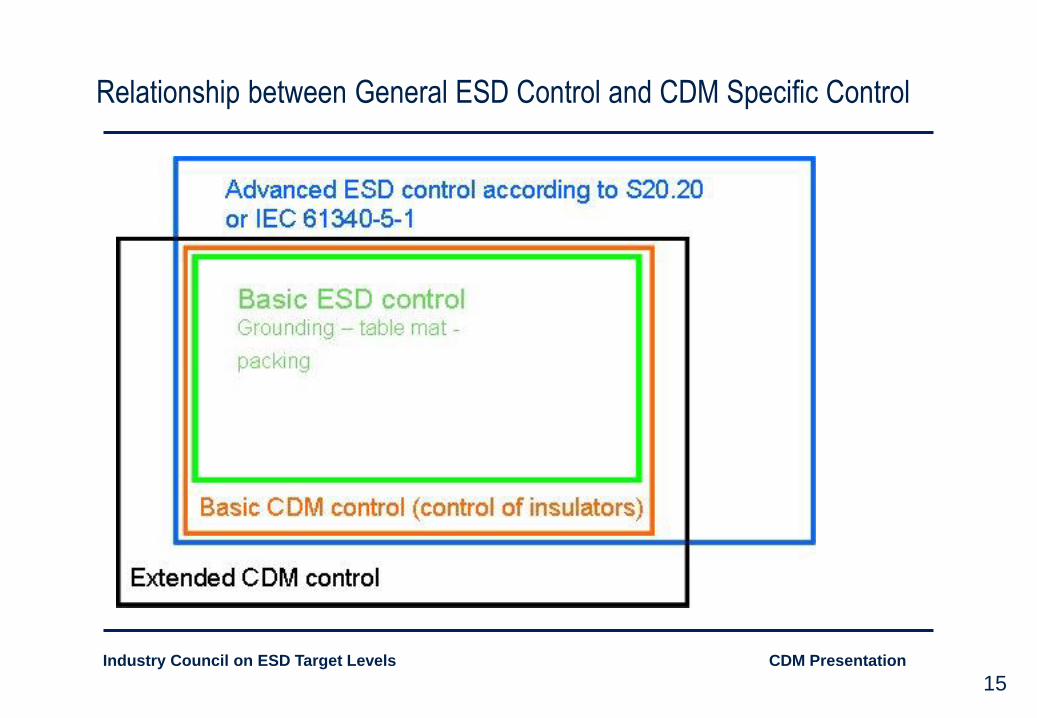
Relationship between General ESD Control and CDM Specific Control
Industry Council on ESD Target Levels CDM Presentation
16
Analysis of FAR Data
• FAR data was collected from various Council members for
over 11 billion shipped IC's.
• Field returns include returns from handling and testing by IC
suppliers, manufacturing of the PCBs and end-customer
returns.
• 949 designs have been included covering automotive,
consumer, memory and discrete products.
• The presented data were collected in the time frame from
2003 to 2007.
Industry Council on ESD Target Levels CDM Presentation
17
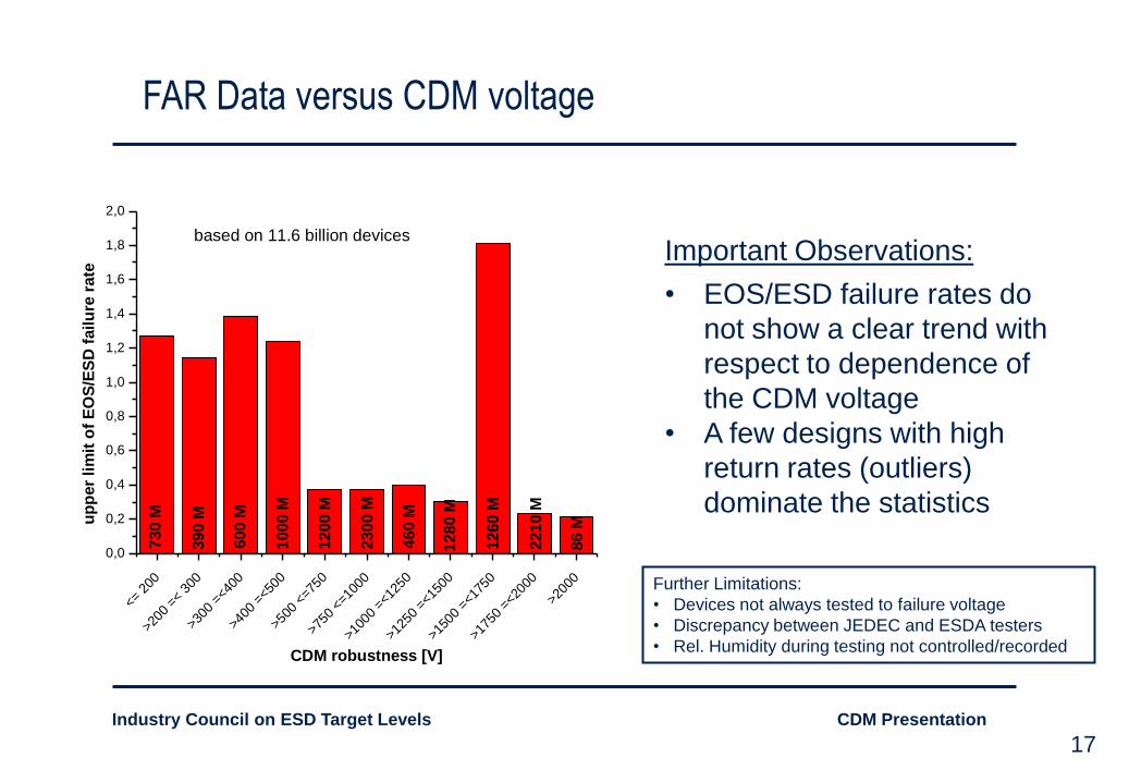
FAR Data versus CDM voltage
Important Observations:
• EOS/ESD failure rates do
not show a clear trend with
respect to dependence of
the CDM voltage
• A few designs with high
return rates (outliers)
dominate the statistics
Further Limitations:
• Devices not always tested to failure voltage
• Discrepancy between JEDEC and ESDA testers
• Rel. Humidity during testing not controlled/recorded
<= 200
>200
=< 3
00
>300
=<400
>400
=<500
>500
<=750
>750
<=10
00
>1000
=<12
50
>1250
=<15
00
>1500
=<17
50
>1750
=<20
00
>2000
0,0
0,2
0,4
0,6
0,8
1,0
1,2
1,4
1,6
1,8
2,0
1280 M
1260
M
221
0 M
86 M
600
M
460 M
230
0 M
1000 M
1200
M
390 M
730 M
based on 11.6 billion devices
up
per
lim
it o
f E
OS
/ES
D f
ailu
re r
ate
CDM robustness [V]
Industry Council on ESD Target Levels CDM Presentation
18
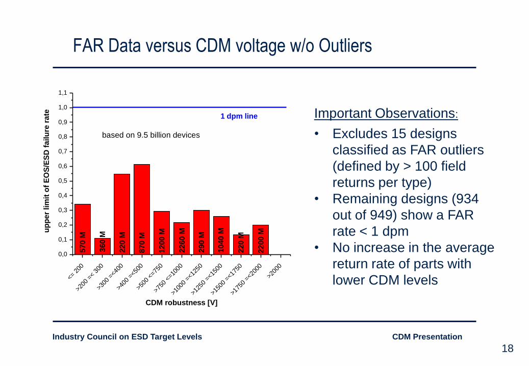
FAR Data versus CDM voltage w/o Outliers
Important Observations:
• Excludes 15 designs
classified as FAR outliers
(defined by > 100 field
returns per type)
• Remaining designs (934
out of 949) show a FAR
rate < 1 dpm
• No increase in the average
return rate of parts with
lower CDM levels
<= 200
>200
=< 3
00
>300
=<40
0
>400
=<50
0
>500
<=75
0
>750
<=1000
>1000
=<12
50
>1250
=<15
00
>1500
=<17
50
>175
0 =<
2000
>2000
0,0
0,1
0,2
0,3
0,4
0,5
0,6
0,7
0,8
0,9
1,0
1,1
1200 M
870
M
22
00 M
220 M
10
40 M
290 M
2260
M
220 M
360 M
570 M
1 dpm line
based on 9.5 billion devices
up
pe
r lim
it o
f E
OS
/ES
D f
ailu
re r
ate
CDM robustness [V]
Industry Council on ESD Target Levels CDM Presentation
19
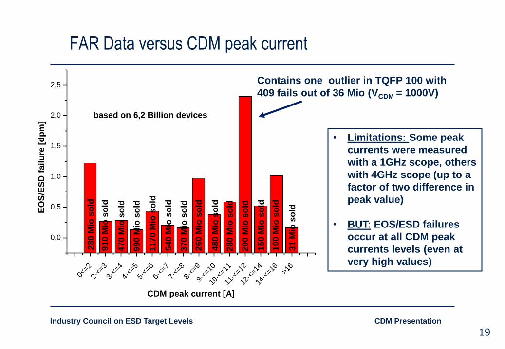
FAR Data versus CDM peak current
Contains one outlier in TQFP 100 with
409 fails out of 36 Mio (VCDM = 1000V)
• Limitations: Some peak
currents were measured
with a 1GHz scope, others
with 4GHz scope (up to a
factor of two difference in
peak value)
• BUT: EOS/ESD failures
occur at all CDM peak
currents levels (even at
very high values)
0<=2
2-<=
3
3-<=
4
4-<=
5
5-<=
6
6-<=
7
7-<=
8
8-<=
9
9-<=
10
10-<
=11
11-<
=12
12-<
=14
14-<
=16
>16
0,0
0,5
1,0
1,5
2,0
2,5
31 M
io s
old
100 M
io s
old
150 M
io s
old
200 M
io s
old
280 M
io s
old
480 M
io s
old
260 M
io s
old
370 M
io s
old
540 M
io s
old
1170 M
io s
old
990 M
io s
old
470 M
io s
old
910 M
io s
old
280 M
io s
old
based on 6,2 Billion devices
EO
S/E
SD
failu
re [
dp
m]
CDM peak current [A]
Industry Council on ESD Target Levels CDM Presentation
20
Analysis of FAR of a CDM Weak Device
Low CDM Effect on FAR
• 140-Pin BGA shows 30 failures out of 67M units shipped
• CDM performance = <125V
• FA shows clear damage on IO gate due to marginal design
• Identical damage was detected on units stressed at 125V
• Implementing advanced CDM controls resulted in 0 FAR for 105M shipped
Control measures can be effective, even for low CDM
Design Issue & Failure Effect
•High speed IO performance required low
capacitance ESD solution in 90nm
•Low capacitance solution = Low CDM
•Device pins were therefore clearly
susceptible to field failures
•At the failure threshold current level for
CDM discharge, IO damage is expected
FA indicated this expected damage
IO
Damage
Industry Council on ESD Target Levels CDM Presentation
21
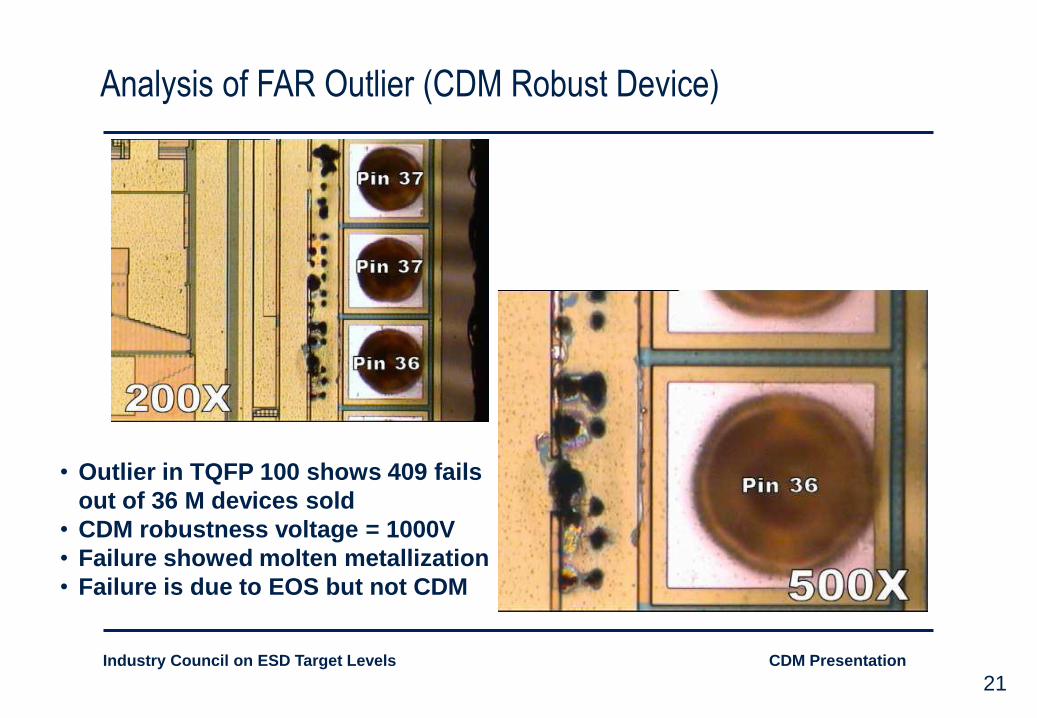
Analysis of FAR Outlier (CDM Robust Device)
• Outlier in TQFP 100 shows 409 fails
out of 36 M devices sold
• CDM robustness voltage = 1000V
• Failure showed molten metallization
• Failure is due to EOS but not CDM
Industry Council on ESD Target Levels CDM Presentation
22
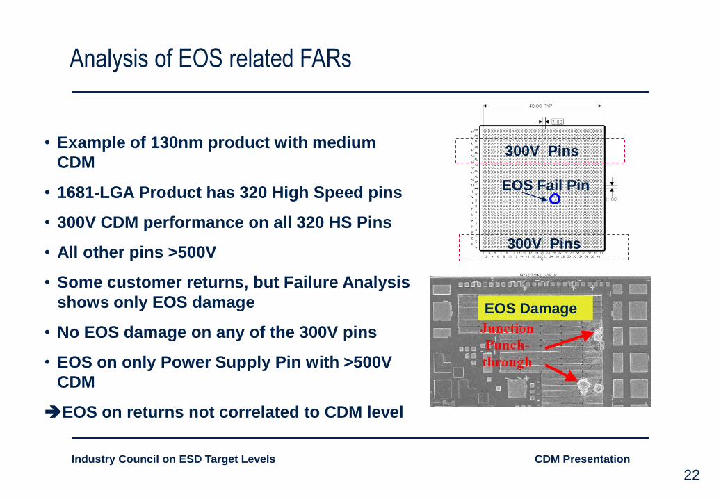
Analysis of EOS related FARs
• Example of 130nm product with medium
CDM
• 1681-LGA Product has 320 High Speed pins
• 300V CDM performance on all 320 HS Pins
• All other pins >500V
• Some customer returns, but Failure Analysis
shows only EOS damage
• No EOS damage on any of the 300V pins
• EOS on only Power Supply Pin with >500V
CDM
EOS on returns not correlated to CDM level
EOS Fail Pin
300V Pins
300V Pins
EOS Damage
Industry Council on ESD Target Levels CDM Presentation
23
Conclusions from FAR Data Analysis
• EOS/ESD FARs can appear for any level of CDM from <100 V
to >2000 V
• FARs with clear CDM damage can be seen for ICs with very
low CDM passing level
• Proven CDM-type events occasionally occur during the ramp-
up phase of a new handling/testing process at the IC supplier.
• FARs during ramp-up can also occur for devices with greater
than 500 V CDM robustness.
Industry Council on ESD Target Levels CDM Presentation
24
Conclusions from FAR Data Analysis
• Addressing the failure mechanism with proper ESD
control measures solves the problem. Usually only a
minor effort combined with a low investment in cost is
required.
CDM field fails can occasionally occur with
significant return rates during ramp-up. This has to
be solved by ESD control measures.
Industry Council on ESD Target Levels CDM Presentation
25
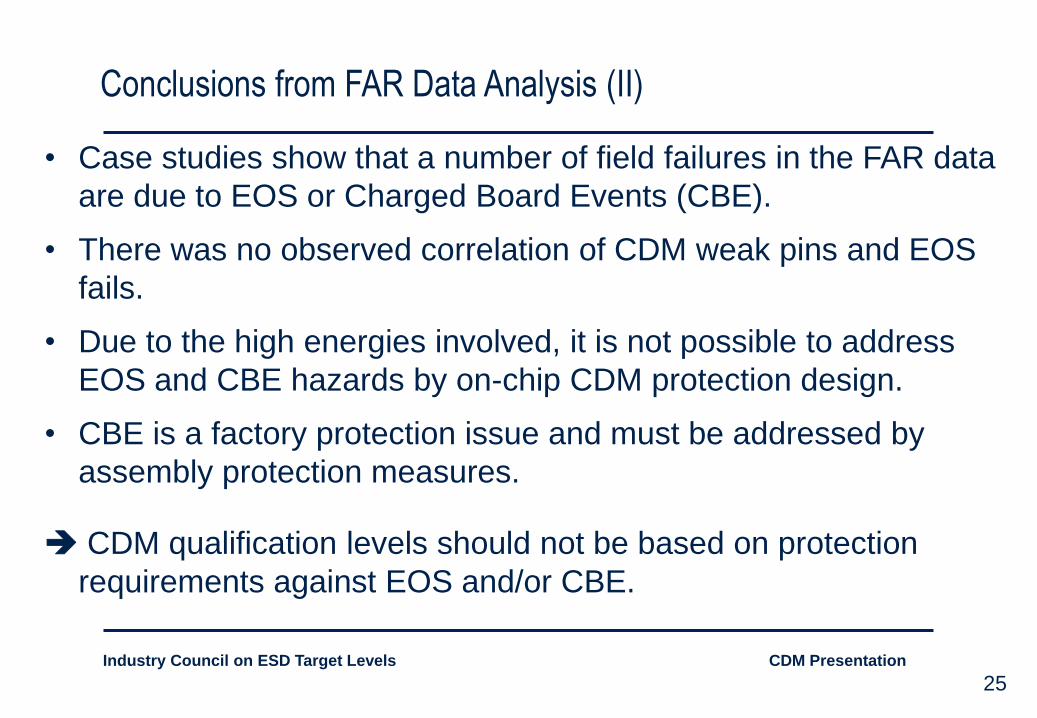
Conclusions from FAR Data Analysis (II)
• Case studies show that a number of field failures in the FAR data
are due to EOS or Charged Board Events (CBE).
• There was no observed correlation of CDM weak pins and EOS
fails.
• Due to the high energies involved, it is not possible to address
EOS and CBE hazards by on-chip CDM protection design.
• CBE is a factory protection issue and must be addressed by
assembly protection measures.
CDM qualification levels should not be based on protection
requirements against EOS and/or CBE.
Industry Council on ESD Target Levels CDM Presentation
26
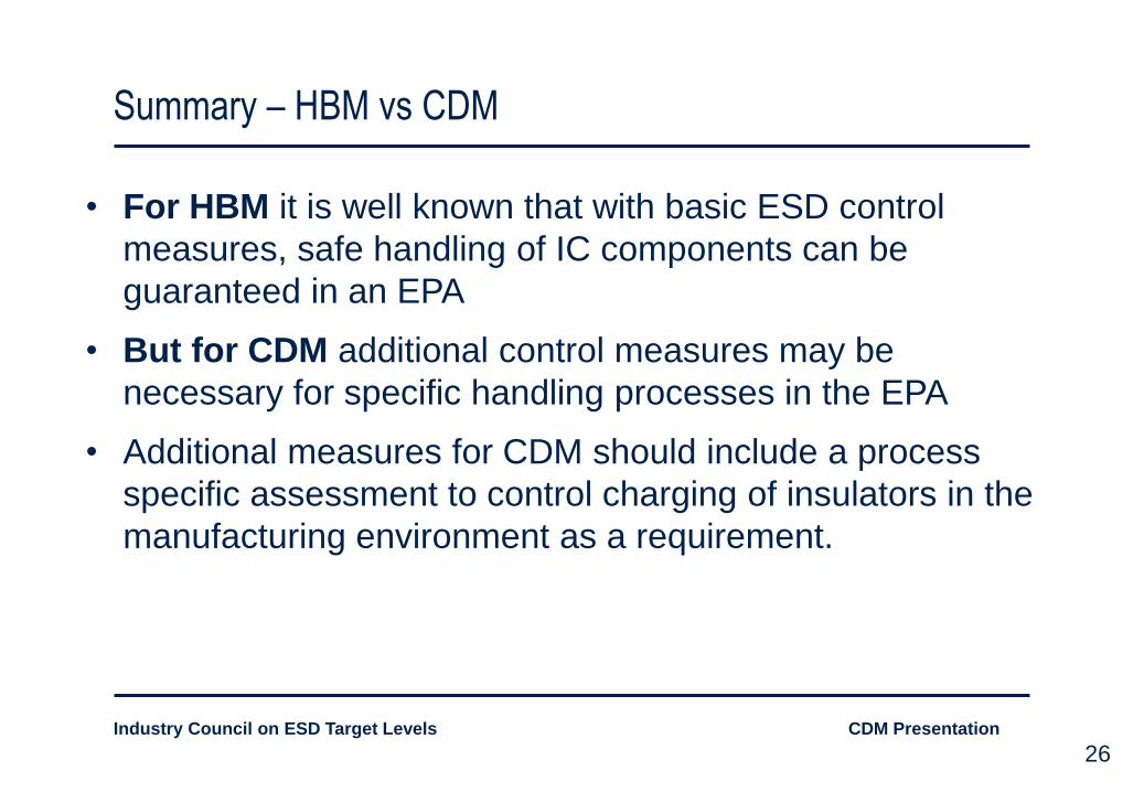
Summary – HBM vs CDM
• For HBM it is well known that with basic ESD control
measures, safe handling of IC components can be
guaranteed in an EPA
• But for CDM additional control measures may be
necessary for specific handling processes in the EPA
• Additional measures for CDM should include a process
specific assessment to control charging of insulators in the
manufacturing environment as a requirement.
Industry Council on ESD Target Levels CDM Presentation
27
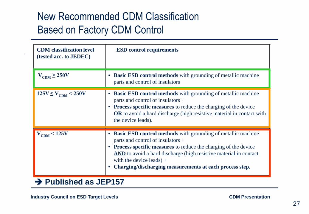
New Recommended CDM Classification
Based on Factory CDM Control
CDM classification level
(tested acc. to JEDEC)
ESD control requirements
VCDM ≥ 250V • Basic ESD control methods with grounding of metallic machine
parts and control of insulators
125V ≤ VCDM < 250V • Basic ESD control methods with grounding of metallic machine
parts and control of insulators +
• Process specific measures to reduce the charging of the device
OR to avoid a hard discharge (high resistive material in contact with
the device leads).
VCDM < 125V • Basic ESD control methods with grounding of metallic machine
parts and control of insulators +
• Process specific measures to reduce the charging of the device
AND to avoid a hard discharge (high resistive material in contact
with the device leads) +
• Charging/discharging measurements at each process step.
Published as JEP157
Industry Council on ESD Target Levels CDM Presentation
28
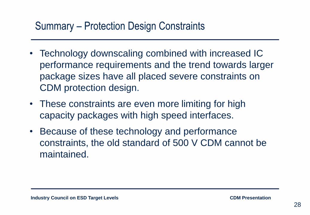
• Technology downscaling combined with increased IC
performance requirements and the trend towards larger
package sizes have all placed severe constraints on
CDM protection design.
• These constraints are even more limiting for high
capacity packages with high speed interfaces.
• Because of these technology and performance
constraints, the old standard of 500 V CDM cannot be
maintained.
Summary – Protection Design Constraints
Industry Council on ESD Target Levels CDM Presentation
29
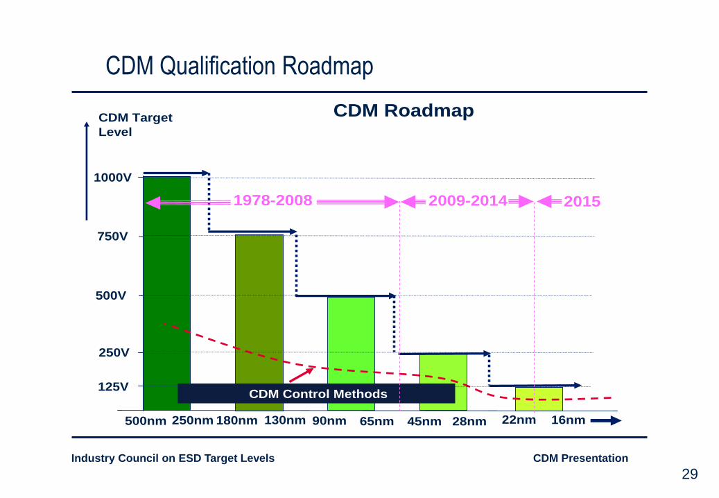
CDM Qualification Roadmap
1000V
750V
500V
250V
125VCDM Control Methods
CDM Target
Level
CDM Roadmap
16nm22nm28nm45nm65nm90nm130nm180nm250nm500nm
1978-2008 2009-2014 2015
Industry Council on ESD Target Levels CDM Presentation
30
Q & A
Q: If the production areas have basic control for ESD, would these methods also provide the necessary protection for CDM?
A: If the basic controls are in place and include control of insulators, then the chances for ESD events of any kind would be minimized
Q: What are the main weak points for CDM ESD control in manufacturing?
A: In contrast to controls for HBM, ESD controls for CDM rely on controlling the charge on insulators and controlling discharges to the conductors of the manufactured devices.
Industry Council on ESD Target Levels CDM Presentation
31
Q & A
Q: How is it determined that lower than 500V CDM are really
safe?
A: It has been proven that even 100V CDM parts can be
manufactured if appropriate CDM control measures are
taken. The same assessment of ESD control measures and
fail return data show that devices with 250V CDM are equally
safe as 500V parts in typical modern manufacturing sites.
Q: If the specifications are meant for all pins of a package,
would it not make sense to require higher levels for the
corner pins?
A: With the automated pick and place tools today, any of the
pins could make first contact. All of the pins need to be
considered, the corner pins should not be treated differently.
Industry Council on ESD Target Levels CDM Presentation
32
Q & A
Q: What if the customers are not confident that the subcons have
the control measures to match the new requirements
A: Simply staying at the old levels will not address the design
challenges. It should be noted that:
• Customer demands for better IO performance will place more stress
on achieving the old target levels.
• Efforts to improve CDM protection in the manufacturing facilities need
to continue to be a focus area if we are to meet these challenges.
• In addition to the basic CDM protection measures, an analysis of the
production lines should be completed. This is especially critical during
introduction of new process steps or during product ramp-up
Industry Council on ESD Target Levels CDM Presentation
33
Q & A
Q: Will CDM change from die to package level? Will the die have greater risk in assembly onto a board
A: In most cases, bare die or wafer level MLF show higher peak current levels than the same die in a package. If the die has the same connectivity to the board as the package, it could have a higher risk of charged board damage. Care must be taken to place the die away from insulators on the board that could charge up during assembly.
Q: Are charge board events (CBE) related to CDM and shouldn’t IC pins be designed to handle CBE?
A: Board level aspects of CBE (much greater capacitance) results in failures that are much more severe, like EOS. Component IC protection cannot be designed to handle CBE events, which can be large and vary from application to application. Additional system level EOS protection must be provided.
Industry Council on ESD Target Levels CDM Presentation
34
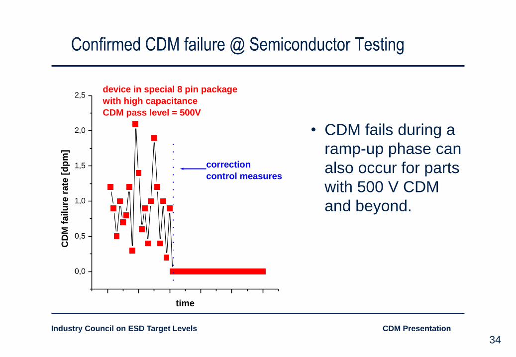
Confirmed CDM failure @ Semiconductor Testing
0,0
0,5
1,0
1,5
2,0
2,5
correction
control measures
device in special 8 pin package
with high capacitance
CDM pass level = 500V
CD
M f
ailu
re r
ate
[d
pm
]
time
• CDM fails during a
ramp-up phase can
also occur for parts
with 500 V CDM
and beyond.


