41
Chemical characterization of semiconductor nanostructures by energy filtered PEEM S. Heun TASC-INFM Laboratory, Area di Ricerca di Trieste, Basovizza, SS-14, Km 163.5, 34012 Trieste, ITALY

Chemical characterization of semiconductor nanostructuresby energy filtered PEEM
S. Heun
TASC-INFM Laboratory, Area di Ricerca di Trieste, Basovizza, SS-14, Km 163.5, 34012 Trieste, ITALY

Outline
A brief introduction to spectromicroscopyThe SPELEEM at Elettra
SPELEEM = spectroscopic photoemission and low energy electron microscope
Application example:AFM local anodic oxidationSi oxidesGaAs oxides

MotivationWhy XPS?
chemical state informationsurface sensitiveease of quantificationnondestructive
Why spectromicroscopy ?(semicond.) nanostructures: self-organization, lithographydevicesdiffusion, segregationalloying (silicide formation)catalysis, chemical wavessurface magnetism (XMCD)

Location of TASC and Elettra
Elettra
TASC-INFM

Elettra Beamlines
exit beamline source
1.1L TWINMIC short id
1.2L Nanospectroscopy id
1.2R FEL (Free-Electron Laser) -
2.2L ESCA Microscopy id
2.2R SuperESCA id
3.2L Spectro Microscopy id
3.2R VUV Photoemission id
4.2 Circularly Polarised Light id
5.2L SAXS (Small Angle X-Ray Scattering) id
5.2R XRD1 (X-ray Diffraction) id
6.1L Material science bm
6.1R SYRMEP (SYnchrotron Radiation for MEdical Physics) bm
6.2R Gas Phase id
7.1 MCX (Powder Diffraction Beamline) bm
7.2 ALOISA (Advanced Line for Overlayer, Interface and Surface Analysis) id
8.1L BEAR (Bending magnet for Emission Absorption and Reflectivity) bm
8.1R LILIT (Lab of Interdisciplinary LIThography) bm
8.2 BACH (Beamline for Advanced DiCHroism) id
9.1 IRSR (Infrared Synchrotron Radiaton Microscopy) bm
9.2 APE (Advanced Photoelectric-effect Experiments) id
10.1L X-ray microfluorescence bm
10.1R DXRL (Deep-etch Lithography) bm
10.2L IUVS (Inelastic Ultra Violet Scattering) id
10.2R BAD Elph id
11.1 XAFS (X-ray Absorption Fine Structure) bm
11.2 XRD2 (X-ray Diffraction) id
1
23
4
5
6

Scanning vs. direct imaging type
Photon optics is demagnifying the beam:Scanning Instrument
Whole power of XPS in a small spot mode.Flexibility for adding different detectors.Rough surfaces can be measured.Limited use for fast dynamic processes.Lower lateral resolution than imaging instruments
Electron optics to magnify irradiated area:Imaging Instrument
High lateral resolution (20 nm).Multi-method instrument (XPEEM/PED).Excellent for monitoring dynamic processes.Poorer spectroscopic ability.Sensitive to rough surfaces.
Monochromaticlight
Sample(scanned)
Photo-emissiondetector
Detector hv
Object plane
Object lensBackfocal planeStigmator
Intermediate imageIntermediatelens
Projectivelens
Image planeMCPScreen CCD camera
Sample
Intermediate image
e-

Outline
A brief introduction to spectromicroscopyThe SPELEEM at Elettra
SPELEEM = spectroscopic photoemission and low energy electron microscope
Application example:AFM local anodic oxidationSi oxidesGaAs oxides

The SPELEEM at ElettraSpectroscopic photoemission and low energy electron microscope

The SPELEEM at ELETTRA

The energy filter
R = 100 mmPass Energy = 900 V

Modes of Operation
XPEEMLEEM
PESELS
PEDLEED

XPEEM: Spectroscopic Microscopy
Images from a Field Effect Transistor (FET) at different binding energies.Photon energy 131.3 eV.

XPEEM: Core Level Spectroscopy

Imaging of Dispersive Plane
W{110} clean surfaceW 4f core level hv = 98 eVResolution 210 meV
(1) Riffe et al., PRL 63 (1989) 1976.(2) Webelements
SCLS (eV)
W7/2-W5/2 BE diff. (eV)
Gauss. Broad. (eV)
Alpha S
Gamma S (eV)
Alpha B
Gamma B (eV)
parameter
0.3040.321
2.142.2 (2)
0.210.04
Fixed0.063
Fixed0.084
Fixed0.035
Fixed0.06
Our fitRef. (1)

Lateral resolution
C 1s image (hv= 350 eV, KE = 62 eV)
Lateral resolution: 32 nm
inte
nsity
(a.u
.)100806040200
distance (pixel)
lateral resolution:0.7 * (4 pixel /435 pixel ) * 5000 (nm)= 32 nm acquisition time: 1min

Outline
A brief introduction to spectromicroscopyThe SPELEEM at Elettra
SPELEEM = spectroscopic photoemission and low energy electron microscope
Application example:AFM local anodic oxidationSi oxidesGaAs oxides

Motivation
Lithography for fabrication of state-of-the-art semiconductor nanostructuresBasic research and quantum device applicationsApproaches:
Traditional lithographyProximal probes (STM or AFM)
H.C. Manoharan, C.P. Lutz, D.M. Eigler: Nature 403 (2000) 512

Local Anodic Oxidation (LAO)
Water electrolysis H2O → H+ + OH-.OH- groups migrate towards the sample.Oxide penetration induced by the intense local electric field.
Versatile tool at relatively low costHigh lateral resolution but small area

Z
Z
Z
Z
GaAs AlGaAs GaAs
LAO on GaAs/AlGaAsBefore oxidation:
After oxidation:

Setup for Lithography on GaAs
Thermomicroscope Microcope CP-Resource
Plexiglass hood
N2 +H2O
water bottle
AFM
voltage sourceAFM
camera Hygrometer

Quantum Point Contact
x
Y
Electronflow
Vgate
-1 0 1 2 30
1
2
3
30 K1.4 K
Cond
ucta
nce
(2e2 /h
)
IPG voltage(V)
G. Mori et al, JVST B 22 (2004) 570.

Why Spectroscopic Microscopy?
Lack of information on the oxidation process and on the chemical nature of the oxides.Lack of reliable microscopic techniques able to perform chemical analysis on such small structures.
Understand the composition of the AFM-grown oxides (electrical and chemical properties, effect of oxidation parameters).Improve the fabrication of devices with LAO.
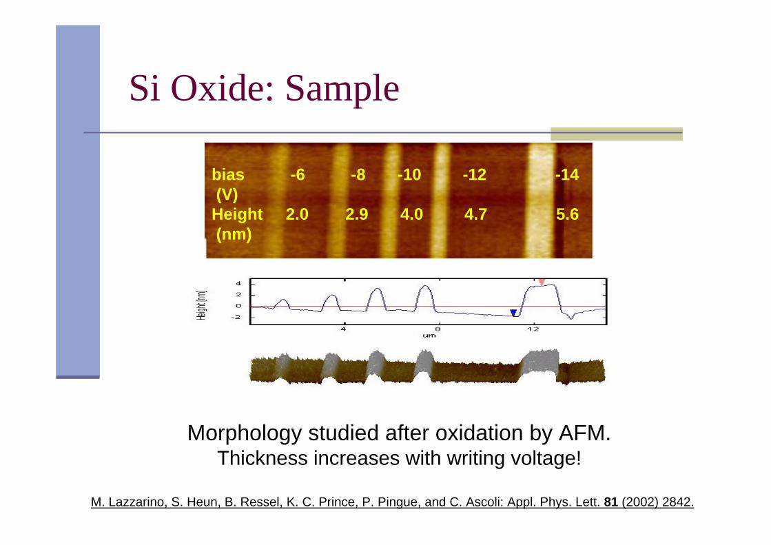
Si Oxide: Sample
M. Lazzarino, S. Heun, B. Ressel, K. C. Prince, P. Pingue, and C. Ascoli: Appl. Phys. Lett. 81 (2002) 2842.
Morphology studied after oxidation by AFM.Thickness increases with writing voltage!
bias -6 -8 -10 -12 -14(V)Height 2.0 2.9 4.0 4.7 5.6(nm)

Si Oxide: Image Contrast at Si 2p
Field of view 12 µm, hv = 132.5 eV, energy resolution: 1 eV
M. Lazzarino, S. Heun, B. Ressel, K. C. Prince, P. Pingue, and C. Ascoli: Appl. Phys. Lett. 81 (2002) 2842.
Binding energy 104.7 eV
a-14V
-12V
-10V
-8V
Binding energy 102.3 eV
b

Si Oxide: Spectroscopy at Si 2p
Spectra show high unformity of each stripeBulk silicon peak: position and width constantNative oxide: SiO2 peak (3.9 eV shifted)AFM oxide shows higher binding energyThere is no evidence of broadeningSpectra explain contrast inversion
M. Lazzarino, S. Heun, B. Ressel, K. C. Prince, P. Pingue, and C. Ascoli: Appl. Phys. Lett. 81 (2002) 2842.
110 109 108 107 106 105 104 103 102 101 100 99 98 97 96 950.0
0.2
0.4
0.6
0.8
1.0
native oxideAFM oxide
Inte
nsity
(a.u
.)
binding energy (eV)

Si Oxide: Spectroscopy at Si 2p
M. Lazzarino, S. Heun, B. Ressel, K. C. Prince, P. Pingue, and C. Ascoli: Appl. Phys. Lett. 81 (2002) 2842.
104.7eV
102.3eV
ba
110 109 108 107 106 105 104 103 102 101 100 99 98 97 96 950.0
0.2
0.4
0.6
0.8
1.0
native oxideAFM oxide
Inte
nsity
(a.u
.)
binding energy (eV)

Si Oxide: Writing Voltage Effect
14V14V
nativenative
12V12V
10V10V
8V8V
1.0
0.8
0.6
0.4
0.2Nor
mal
ized
Pho
toem
issi
on In
tens
ity
110 105 100 95Binding Energy (eV)
: native oxide: 14 V: 12 V: 10 V: 8 V
Si 2p
siliconoxide
bulksilicon
M. Lazzarino, S. Heun, B. Ressel, K. C. Prince, P. Pingue, and C. Ascoli: Appl. Phys. Lett. 81 (2002) 2842.
ΔE = 3.97 eV (native)ΔE = 4.62 eV (U = 14V)ΔE = 4.46 eV (U = 12V)ΔE = 4. 41 eV (U = 10V)ΔE = 4.39 eV (U = 8V)
Shift (Sibulk - SiOx) increases with increasing writing voltage (oxide thickness).

Si Oxide: Charging Effects
H. Kobayashi, T. Kubota, H. Kawa, Y. Nakato, and M. Nishiyama: Appl. Phys. Lett. 73 (1998) 933.
+ +
+ +
+ +
Intensity decreases due to escape depth
effectCharged (yellow)
layer contribution is more important
Squared points: our data
Line: Kobayashi model

GaAs Oxide: Photon Exposure
AFM after: height 13nm
AFM before: height 18nm
Images taken with secondary electronsPhoton energy: 125 eVKinetic energy: 4 eVField of view: 10 µmOne image every 2 sec

GaAs Oxide: Desorption
Writing speed 0.5 µm/sHumidity 50 %
Photon energy 130 eVPhoton flux 1017 ph cm-2sec-1
Before photon exposure After hours of exposure
12V
1μm12V14V
16V
14V10V
hv

Height reduction vs. exposure time
We observe a linear relation between exposure time and height reduction.A dependence on other oxidation parameters (bias, speed) could not be detected.
hv = 130 eV = 9.5 nm

Spectra From AFM GaAs Oxide
Sample S03BHole (3,2)Writing voltage 15 VStructure height 3 nmImage taken with secondary electrons:
Photon energy: 130 eVKinetic energy: 0.3 eVField of view: 10 µm
Time resolved spectroscopy with SPELEEM using Dispersive Plane (hv = 130 eV)

Spectra From AFM GaAs Oxide
Time resolved spectroscopy with SPELEEM using Dispersive Plane (hv = 130 eV)
2500
2000
1500
1000
Inte
nsity
(a.
u.)
12 10 8 6 4 2Relative Binding Energy (eV)
Exposure Time 3 min 5 min 7 min 13 min 20 min 28 min 43 min 63 min
As 3dhv = 130 eV
1000
800
600
400
200
Inte
nsity
(a.
u.)
12 10 8 6 4 2Relative Binding Energy (eV)
Exposure Time 4 min 6 min 10 min 17 min 25 min 54 min 74 min
Ga 3dhv = 130 eV
As oxide GaAsO 2s
Ga oxides+ GaAs
The As-oxide signal disappeares with time.The Ga-oxide signal remains unchanged (early stage of exposure).

Spectra From AFM GaAs Oxide
The AFM-oxide is mainly composed of Ga2O. After 3 hours exposure, only traces of As-oxides observed in As 3d.Absolute ratio As : Ga = 1 : 5
4000
3500
3000
2500
2000
Inte
nsity
(a.
u.)
888684828078Kinetic energy (eV)
As 3dhv = 130 eV
GaAs
AsO
20x103
15
10
5
0
Inte
nsity
(a.
u.)
110108106104102100Kinetic Energy (eV)
Ga 3dhv = 130 eV
GaAs
Ga2O
Ga2O3
O 2s
after160 min.
after115 min.

A possible model for the desorptionOur Observations:
The AFM-grown oxide exposed to 130 eV photons desorbs linearly with exposure time.The AFM-oxide is mainly composed of Ga2O with traces of As-oxide.The shape of the Ga peak does not change with exposure time (early stage of desorption).The As-oxides desorb completely after 3 hours of exposure.Not even traces of As-oxides detected in scanning Auger microscopy.
GaAs
Ga2O
Ga2O + As-oxides

The physics underlying the desorption
Does the desorpion depend on the total amount of energy delivered to the system?
No! We delivered the same amount of energy with electrons and conventional XPS but no desorption took place.
Does the photon beam heat up the system enough to locally deoxidize the sample?
No! The oxides are stable up to 400ºC. The calculated local heating is less than 10ºC.
The desorption depends on photon flux and energy!

Thermal stabilityRT 300C 400C 450C
500C 550C 600C
Each annealing step:10 minutes
in N2 atmosphere

The Knotek-Feibelman mechanism
The valence electrons are mainly localized at O atoms.This Auger decay leads to a final state with two vacancies in valence band weakening the bond between Ga and O.
Valence electrons
E
3d
GaInitial state
Valence electrons
E
3d
Ga
Valence electrons
E
3d
Ga
Valence electrons
E
3d
GaFinal state

SummarySi oxide:
The AFM induced oxidation produces chemically uniform, stoichiometric SiO2 with dielectric properties comparable to those of thermal SiO2.
GaAs oxide:The AFM-oxide is mainly composed of Ga2O with traces of As-oxide at the surface.Photon assisted partial desorption of the AFM-grown oxide was observed.All As oxides and the oxygen-rich Ga oxides are desorbed.We proposed a simple model for the dynamics of the desorption.
Acknowledgements
M. Lazzarino, G. Mori, D. Ercolani, B. Ressel, and L. Sorba (Laboratorio TASC-INFM, Area di Ricerca, I-34012 Trieste, Italy)
A. Locatelli, S. Cherifi, A. Ballestrazzi, and K. C. Prince (Sincrotrone Trieste, Area di Ricerca, I-34012 Trieste, Italy)
P. Pingue (NEST-INFM and Scuola Normale Superiore, I-56012 Pisa, Italy)


