Chemical Mechanical Planarization of Copper Damascene StructuresP. Wrschka,a J. Hernandez,a G. S. Oehrlein,a,* and J. King b.c
aDepartment of Physics, The University at Albany, State University of New York, Albany, New York 12222, USAbCybeq Nano Technologies, San Jose, California 94025, USA
Manuscript submitted June 18, 1999; revised manuscript received September 30, 1999.
tepves
s. Itnter-g-
yers
izedlinerre
owing,r areforve(seeh to beo beuiv-
tern
nsity.t col- theden-at- dot-t of
pat-
Copper is beginning to replace aluminum as the interconnemetal in integrated circuits (IC). Not only has Cu the ability to reducthe resistance-capacitance product (RC) delay due to its lower retivity, but also increase the circuit reliability because of its higheelectromigration resistance.1-4 The use of reactive ion etching (RIE)to pattern Cu is impractical, because volatile Cu compounds foonly at elevated temperatures.5 The damascene process provides solution to the problems arising from the lack of a directional metetch capability.6-8 In this approach, the dielectric is patterned by RIE(Fig. 1a), followed by the liner and metal deposition (Fig. 1b). Thliner becomes necessary when using Cu as an interconnect materi
Figure 1. Cross-sectional view after the different process steps for the daascene technique: (a) Patterns are etched into the SiO2. (b) Liner material andmetal are deposited over the whole surface of the patterned wafer. (c) Cremoves the excess liner material and metal. The metal remains only ingaps (trenches/holes) to form the interconnects.
ctesis-r
rmaal
eal to
prevent the rapid diffusion of the Cu into the dielectric. The final sin this process is chemical mechanical polishing (CMP) that remothe excess metal and provides global planarization9 (Fig. 1c). The pla-narization capability is an important advantage of the CMP procesprevents problems associated with the increase of the number of iconnect layers in the multilevel metallization of ICs, where the toporaphy of device structures increases significantly as additional laare stacked on top of one another.10
In order to achieve ideal planarized structures as shown idealin Fig. 1c, the CMP process has to remove the metal and the material evenly without eroding the underlying dielectric. Therefoa high metal and liner to dielectric selectivity is necessary. Lselectivities can lead to the erosion of patterns during overpolishwhich is necessary because the removal rates across the wafeusually not constant. Also, longer polishing times are required regions of low pattern density (low density of metal lines) to remothe larger amounts of metal situated on top of the spacers Fig. 2a, right column). During the overpolishing, regions of higmetal pattern density tend to erode faster since less metal needsremoved to planarize the structures and less dielectric needs tremoved to erode the spacers. A high metal pattern density is eqalent to a low dielectric density; therefore areas of high metal patdensities show higher metal and dielectric removal rates.11
m-
MP the
Figure 2. (a) The time needed to planarize a structure,i.e., to remove theexcess metal to obtain an isolated metal line, depends on the pattern deLess overburden needs to be removed in high pattern density areas (lefumn) as compared to low pattern density areas (right column). (b) Whenhigh pattern density structures are planarized (left) areas of low pattern sity still show some residual metal. (c) During the overpolishing time the pterned dielectric (left) erodes faster as compared to the unpatterned. Theted line indicates the original, uneroded dielectric thickness. The end pointhe CMP process is reached when no residual metal is found in the lowtern density areas (right).
The problems associated with the homogeneous removal of themetal overburden in low and high pattern density areas can be solvedby depositing a sufficiently thick film of metal,since in this fashionthe metal is already planarized before the polishing pad reaches themetal/dielectric interface during the CMP process. However, thisapproach is not feasible for the liner material, which makes achiev-ing high liner/dielectric selectivity very important. Ta and/or TaNliners are frequently used for Cu interconnects.12,13 Ta is a hard(mineral hardness:6.5) and chemically inert metal,14,15which makesit difficult to remove.
The two important consumables for the CMP process are the padand the slurry. The choice of the polishing pad influences the pla-narization rate. A harder pad planarizes a surface faster and causesless dishing of the metal lines.11,16The role of the slurry can be sep-arated into two aspects:particles and chemistry. The choice of theparticles is important to prevent defects,since large or clustered par-ticles can scratch the surface during CMP. This can lead to defects inthe spacers degrading the isolation of the metal line, or it may causedefects in the metal line itself. The choice of the slurry chemistry,such as pH value and etch rate, influence the metal removal rate, themetal/dielectric selectivity, as well as undesired etching and corro-sion of the metal lines.
These issues can affect both the fabrication and ultimate perfor-mance of an IC device. We describe the results of experiments on thepolishing of patterned Cu samples using several slurries. Specialattention was given to the corrosion behavior of the slurries utilizedsince Cu does not passivate as readily as other metals,e.g.,Al.15Thiscan lead to the localized dissolution (corrosion) of Cu lines.
Experimental
CMP tool.—All polishing results in this paper were obtainedwith a Cybeq 3900 (Cybeq Nano Technologies,San Jose, CA) waferpolisher and planarization system. This tool is a three-axis polisherconsisting of a head (wafer carrier), a carousel,and a platen as de-scribed previously.17 The down force on the wafer is set by air pres-sure applied uniformly to the head. For the blanket polishing exper-iments,the polishing pressure was varied between 19 and 33 kPa andthe linear polishing velocity between 26 and 48 m/min. Although theCybeq 3900 tool is capable of polishing six wafers simultaneously,for practical reasons,all experimental runs were performed with oneor two wafer heads. A mounting pad (DF 200/buffed poromeric film,Rodel,Inc., Newark, DE) and a Delrin retaining ring with an innerdiameter slightly greater than that of the wafer were used on the headto hold the wafer in place during polishing. This setup allows foreasy placement and removal of the wafer from the carrier withoutdamage and contamination. This tool incorporates an ex situ paddresser which is used to recondition the surface of the pad after aCMP run. For experiments in which the pad was reconditioned, thepressure exerted by the dresser on the pad was set to 20 psi.
Samples.—Polishing was performed on 150 mm diam Si wafersthat were either covered with a thin film of Cu or thermally grownSiO2. In order to investigate the removal rate selectivity of Cu toSiO2, the 150 mm copper and oxide wafers were polished simulta-neously. The patterned Cu samples (damascene structures) utilizedwere partial wafers 2 3 2 cm in size consisting of an array of dif-ferent sized trenches. These patterned structures as well as the blan-ket Cu wafers contained a Ta liner 50 nm thick to prevent diffusionof the copper into the oxide. The thin films of pure Cu for blanketand patterned wafers were sputter-deposited with a thickness of2.3 mm. The thermally grown oxide had a thickness of 1.5 mm.
To study the removal of the liner material we polished partialwafers, (2 3 2 cm) coated with 350 nm of Ta or TaN, independent-ly from the Cu CMP experiments but under the same experimentalconditions.
Consumables.—The polishing experiments were conducted withfour different slurries: the Rodel slurry QCTT1010 (slurry A1) andthree experimental slurries labeled slurry A2, S1, and S2. The prop-erties of the slurries are shown in Table I. Slurry A1 and experimen-
tal slurry A2 both contain fumed alumina particles and have a pH of4.0 and 3.6,respectively. Experimental slurries S1 and S2, on theother hand, incorporate the same type of silica particles to act as theabrasive and were measured to have a pH value of 3.5 and 3.9,respectively. The slurry chemistries of the three experimental slur-ries differ only in the amount of an additive to adjust the etch rates(discussed in detail below). An oxidizer (hydrogen peroxide, H2O2)was added to each of the slurries in order to oxidize the copper filmand thus enhance its removal rate. For all of the CMP experimentsperformed in this study, the slurry was fed to the polishing platenthrough a masterflex pump system at a flow rate of 300 mL/min.Figure 3 shows the particle size distributions for slurry A1 and S1obtained from a laser scattering particle size distribution analyzer(Horiba LA-910). Only incomplete data is available for slurry A2.With 128 nm 6 36 nm,the silica slurry has a smaller mean particlediameter than the alumina slurry (316 nm 6 25 nm),but shows asecond, smaller peak in the size distribution at 600 nm (see inset,particle counts only from slurry S1).
The polishing pads (IC 1400 k-groove) were supplied by Rodel,Inc. The IC 1400 is composed of the IC1000 stacked on top of theSuba IV. The properties of this pad, especially its microstructurehave been described by Hernandez et al.18
Before each polishing run,the pad was soaked with slurry for 30sto fully charge the pad with abrasive particles. After each run, thewafers were brushed and rinsed in deionized water and dried withcompressed N2. This cleaning procedure removes most of the residuesof slurry particles from the wafers and does not introduce any defects.For the pattern polishing study no brushing was performed so as notto interfere with the performance of the above mentioned slurries. Thepad was only rejuvenated (dressed) for one minute when we startedpolishing experiments with a different slurry.
Removal rate determination.—Thickness and uniformity of theCu films were obtained by using a four point probe to measure the
Table I. Slurry properties.
Particle Etch rate Removal rateSlurry pH type (nm/min) (nm/min)
Figure 3.Particle size distribution as measured with a laser scattering ana-lyzer. The mean particle diameter for slurry S1 is smaller than that for A1, butS1 shows a small,second peak (inset) at larger particle sizes.
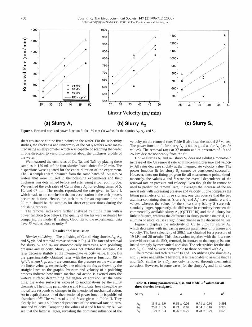
Figure 4.Removal rates and power function fit for 150 mm Cu wafers for the slurries A1, A2, and S1.
sheet resistance at nine fixed points on the wafer. For the selectivitystudies,the thickness and uniformity of the SiO2 wafers were meas-ured using an ellipsometer which was capable of scanning the waferin one direction to yield information about the thickness profile ofthe wafer.
We measured the etch rates of Cu,Ta, and TaN by placing thesesamples in 150 mL of the four slurries listed above for 20 min. Thedispersions were agitated for the entire duration of the experiment.The Cu samples were obtained from the same batch of 150 mm Siwafers that were utilized in the polishing experiments and theirthickness was determined before and after using a four point probe.We verif ied the etch rates of Cu in slurry A2 for etching times of 5,10, and 67 min. The results reproduced the rate given in Table I,which leads to the conclusion that no acceleration in the etch processoccurs with time. Hence, the etch rates for an exposure time of20 min should be the same as for short exposure times during thepolishing process.
The removal rates were further analyzed by fitting them with apower function (see below). The quality of the fits were evaluated bycomparing the model R2 values. Good fits to the experimental datahave R2 values close to unity.19
Results and Discussion
Blanket polishing.—The polishing of Cu utilizing slurries A1, A2,and S1 yielded removal rates as shown in Fig. 4. The rates of removalfor slurry A1 and A2 are monotonically increasing with polishingpressure and velocity. Slurry S1 does not exhibit this increase. Allrates decrease slightly at the intermediate velocity value. If one fitsthe experimentally obtained rates with the power function,RR 5kpavb, where k, p, and v are constants,the pressure on the wafer andthe linear velocity, respectively, one obtains the fits as shown by thestraight lines on the graphs. Pressure and velocity of a polishingprocess indicate how much mechanical action is exerted onto thewafer’s surface, determining the degree of abrasion. At the sametime, the wafer surface is exposed to modifications by the slurrychemistry. The fitting parameters a and b indicate, how strong the re-moval rate responds to changes in the mentioned mechanical action.An in depth discussion of the mentioned power function is publishedelsewhere.17,18 The values of a and b are given in Table II. Theyclearly indicate a sublinear dependence of the removal rate on pres-sure and velocity. Comparing the values of a and b for slurry A1, wesee that the latter is larger, revealing the dominant influence of the
velocity on the removal rate. Table II also lists the model R2 values.The power function fit for slurry A2 is not as good as for A1 (see R2
values). The removal rates at 37 m/min and at pressures of 19 and26 kPa deviate noticeably from the fit.
Unlike slurries A1 and A2, slurry S1 does not exhibit a monotonicincrease of the Cu removal rate with increasing pressure and veloci-ty. All r ates decrease slightly at the intermediate velocity value. Thepower function fit for slurry S1 cannot be considered successful.However, since our fitting program fits all measurement points simul-taneously, the values a and b state the overall dependence of theremoval rate on pressure and velocity. Even though the fit cannot beused to predict the removal rate, it averages the increase of the re-moval rate with increasing pressure and velocity. If one compares thefitting parameters of all three slurries,one can observe that the twoalumina-containing slurries (slurry A1 and A2) have similar a and bvalues,whereas the values for the silica slurry (slurry S1) are sub-stantially larger. Apparently, the difference in chemistry between thecommercially available slurry A1 (QCTT1010) and the S1 slurry haslittle influence, whereas the difference in slurry particle material, i.e.,alumina or silica,causes a significant change in the discussed values.
Figure 5 displays the selectivity of Cu to SiO2 for slurry A1,which decreases with increasing process parameters of pressure andvelocity. The best selectivity of 206:1 was obtained for a pressure of19 kPa and 26 m/min. This observation together with the low ratesare evidence that the SiO2 removal, in contrast to the copper, is dom-inated strongly by mechanical abrasion. The selectivities for the slur-ries A2, S1, and S2 were comparable to those obtained with A1.
The removal and etch rates of Ta and TaN utilizing the slurries A1and S1 were negligible. Therefore, it is reasonable to assume that Taand TaN, similar to SiO2, are only removed through mechanicalabrasion. However, in some cases,for the slurry A1 and in all cases
Table II. Fitting par ameters k, a, b, and model R2 values for allthr ee slurr ies investigated.
for the slurry S1, it was found that the liner film had partially delam-inated after polishing. Further investigation revealed that for the alu-mina slurry A1, the liner film delaminated only as a result of the fourpoint probe measurement prior to polishing. The film peeled only inthe direct vicinity where the probe had touched the sample. The fourpoint probe measurement is invasive, i.e., it introduces defects intothe surface of the film. The Ta liner possesses high internal stresswhen deposited on SiO2.
20 Therefore, these films easily lose adhe-sion (peeling) when subjected to surface damage. It is possible thatthe small amount of larger particles present in slurry S1 (see inset ofFig. 3) introduced surface defects in the Ta film that caused theobserved delamination.
Pattern polishing.—Erosion and Cu line recess.—After the ini-tial CMP of blanket Cu wafers,we focused on the chemical mechan-ical polishing of Cu patterns and compared the four different slurriesA1, A2, S1, and S2. Erosion of the SiO2 spacers,dishing and surfacetopography of the copper lines,scratching, and contamination of thestructures were examined.
No scratches were observed for polishing with all four slurries asshown in the micrographs of Fig. 6. The results for slurry S2 are notdisplayed because no differences were observed when comparedwith slurry S1.
Figure 5.Cu/SiO2 selectivity using A1 slurry as a function of linear velocityand pressure.
Figure 7a displays an unpolished set of trenches in a cross-sec-tional view. The width of the two outer trenches is 3.3 mm and thatof the center trench is 3.9 mm. These trenches have a uniform depthof 920 nm and were initially covered with 2.3 mm of Cu. As shownin Fig. 7b, well-planarized structures are obtained after polishingwith slurry A1. Upon closer inspection,however, one can observethat the oxide spacers are eroded and although the Cu lines showvery little dishing they are slightly recessed.
Figure 8 shows two 1 mm wide trenches with strongly recessedCu lines. The schematic drawing in Fig. 9 explains this in moredetail. If patterns are overpolished they can erode. Because the metalpolishes faster than the dielectric, the metal will always stay at orbelow the level of the neighboring spacer, which causes a thinningof the metal lines as soon as the SiO2 is eroded. Due to pad bendingspacers can appear rounded and the adjacent metal lines dished. Inaddition to dishing, the metal lines can be recessed, so that oneobserves a step from the spacer down to the Cu wire. The pad we uti-lized is stiff enough to keep spacer rounding and Cu line dishing toa minimum. For our experiments the amounts of rounding and dish-ing were small in comparison to the “step” height (see Fig. 9).
Hence, it is reasonable to assume that the metal recess originatesmainly from a chemical etch rather than from pad bending. Anisotropic etch leaves a Cu line of uniform thickness behind, whereasa line eroded by the pad is thinner at the center than at the edges.This assumption is verif ied when plotting the Cu line recess vs. etchrate as shown in Fig. 10 for all four slurries. Slurry S2 shows the leastamount of Cu line recess while slurry S1 shows the greatest which isconsistent with the etch rate experiments on Cu that were mentionedpreviously. Finally, it should be noted that the SiO2 spacer erosion iscomparable for all four slurries.
Corrosion of submicrometer Cu lines.—Severe corrosion of Cu linesoccurs only for the S1 slurry and only for the smallest Cu linewidth,i.e., 0.69 mm, to be found on this particular type of patterned wafer.Neither the slurry A1, A2, or S2 display the corrosion shown inFig. 11b. The micrographs in Fig. 11a and c exhibit an uncorrodedCu line of the same type from a sample polished with slurry A2 andS2. The corrosion is presumably caused by the presence of hydroni-um ions (H3O
1). If the Cu is first oxidized (e.g., by oxidizer H2O2)to one of its simple oxides (i.e., CuO or Cu2O) then the hydroniumions (H3O
1) facilitate their dissolution.15,21
Moreover, we observed that the degree of corrosion is alsodependent on the pattern density. The same Cu lines are less corrod-ed in regions of high pattern density than in areas of low pattern den-sity. Figure 12a displays the strongly corroded Cu line in a low pat-tern density area,whereas Fig. 12b is taken using an area of high pat-
Figure 6.Top down view of a patterned sample polished with three different slurries. No defects are introduced during the planarization process by either slurry.
Figure 7.Cross section of damascene structures:(a) before CMP; (b) after CMP.
tern density and shows less corrosion. The fact that only submi-crometer Cu lines are subject to corrosion may be attributed to thehigher inner stress of small Cu lines. Stress decreases the activationenergy for certain chemical reactions.22 However, the correlationbetween pattern density and degree of corrosion could be due to thelocally different consumption of the hydronium ions. This isexplained in more detail in Fig. 13a and b, which are cross-section-al schematics of Fig. 12a and b. One can assume that during the pol-ishing process,a constant flux of hydronium ions is provided to thepolished surface. The consumption of these ions depends directly onthe amount of Cu present at the wafer surface resulting in high con-centrations in areas with only a few Cu lines (low pattern density)and low concentrations in areas with a lot of Cu lines (high patterndensity). To the left of the 0.69 mm trench of Fig. 13a is a large spac-er, several tens of micrometers wide, representing an area,where nohydronium ions are consumed due to the lack of Cu. This can pro-mote the local increase of H3O
1, inducing the corrosion of the near-by Cu line. The small and less corroded Cu line in Fig. 12b is onlyseparated on each side by a relatively narrow spacer followed by alarge Cu wire. The local pattern density in Fig. 13b is much higherthan in Fig. 13a,providing an increased consumption of the activecorrosive substance (H3O
1). In regions of high pattern density, thecorrosion is only caused by the internal stress of small Cu lines.
Figure 8.Cross section of a damascene structure after CMP with recessed Culines.
Some issues that need further investigation are the Ta linerremoval and the correlation between slurry particle material andcontamination. Figure 14 shows patterns polished with slurry A1 and
Figure 9.Generic features of polished patterns that may arise as a result ofCMP.
Figure 10.The Cu line recess shows a direct correlation to the etch rates forall slurries tested. Therefore the recess is due to the chemical etching of theslurry and not due to pad bending (dishing).
Figure 11.Cross sections of 0.69 mm wide Cu lines after polishing with (a) slurry A2, (b) slurry S1, and (c) slurry S2. Only slurry S1 displays severe corrosion.
S1, but only the alumina-based slurry displays Ta residues on theSiO2 spacers even though the amount of overpolishing (sameamount of spacer erosion) for the two samples are comparable. Thedifference in the Ta removal could be explained by the differences inthe particle size distributions of both slurries. Slurry S1 incorporatessmall amounts of larger particles that could aid in the delaminationof the barrier layer. Chemical effects are unlikely to contribute to thisdifference, because both slurries have negligible etch rates for Ta. Ahigher etch rate would yield a higher liner/dielectric selectivity.However, this approach of solving the liner removal issue wouldintroduce problems with the etching and corrosion of the Cu lines.
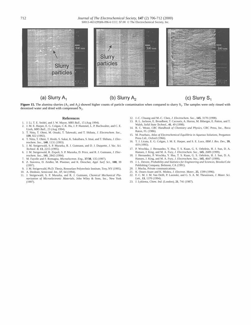
Figure 15 addresses the issue of slurry particle contamination. Incontrast to the slurries A1 and A2, the silica-based slurry S1 revealsfewer slurry particles that adhered to the wafer surface, especially tothe Cu lines. The accumulation of surface charges on the slurry par-ticles and the polished surface could be responsible for this. A meas-ure for this charge accumulation is the zeta potential.11,23At pH 4,alumina (Al2O3) has a positive zeta potential,whereas that of silica(SiO2) is negative. Metal surfaces always have a negative zeta poten-
Figure 12.Pattern density effect on corrosion with 0.69 mm wide Cu linespolished with slurry S1. Small Cu lines showed less corrosion in areas of highpattern density.
Figure 13.Possible explanation for the effect of the pattern density on cor-rosion (schematic).
tial.11 This means that the silica slurry particles are electrostaticallyrepelled from the polished surface, consisting of silica spacers andmetal lines,while the alumina particles are attracted in each case.For the alumina slurries,we found most of the particle contamina-tion on the Cu lines as shown in Fig. 15a. It seems that at the givenpH, the surface charging of the Cu is significant.
Conclusion
This article described generic issues of the CMP process thatmay arise form the choice of slurry. We find that the slurry particletype, i.e. alumina or silica,has a significant influence on the depen-dence of the removal rate on pressure and velocity. Good selectivi-ties were achieved with all four slurries. We have found that in orderto yield reproducible removal rates low etch rates of the slurry chem-istry are necessary, i.e., on the order of 10 nm/min. Furthermore, lowetch rates are required to prevent recess and corrosion of the Culines. We have shown that corrosion is prone to occur on small Culines located in low pattern density areas. The chemical inertness ofthe liner material can lead to residues on the spacers that compro-mise the insulation of the Cu lines. The particle type material canhave an effect on the efficiency of the post CMP clean up. Largeramounts of alumina particles adhered to the Cu lines as compared tothe silica particles.
Acknowledgments
The authors would like to thank Cybeq Nano Technologies,Mit -subishi Materials Corporation, Rodel,and IBM for support of thisstudy.
Figure 14.Only the sample polished with slurry A1 shows Ta residues on theSiO2 spacers, even though both samples were subjected to the same amountof overpolishing. The small amounts of larger particles (600 nm diam) ofslurry S1 could contribute to the delamination of the Ta barrier layer.
Figure 15.The alumina slurries (A1 and A2) showed higher counts of particle contamination when compared to slurry S1. The samples were only rinsed withdeionized water and dried with compressed N2.
References1. J. Li, T. E. Seidel,and J. W. Mayer, MRS Bull., 15 (Aug 1994).2. J. M. E. Harper, E. G. Colgan,C-K. Hu,J. P. Hummel,L. P. Buchwalter, and C. E.
Uzoh,MRS Bull., 23 (Aug 1994).3. T. Nitta, T. Ohmi, M. Otsuki,T. Takewaki, and T. Shibata, J. Electrochem. Soc.,
139, 922 (1992).4. T. Nitta,T. Ohmi,T. Hoshi,S. Sakai,K. Sakaibara,S. Imai,and T. Shibata,J. Elec-
trochem. Soc., 140, 1131 (1993).5. J. M. Steigerwald, S. P. Murarka, R. J. Gutmann,and D. J. Duquette, J. Vac. Sci.
Technol. B, 13, 2215 (1995).6. J. M. Steigerwald, R. Zirpoli, S. P. Murarka,D. Price, and R. J. Gutmann,J. Elec-
trochem. Soc., 141, 2842 (1994).7. M. Fayolle and F. Romagna,Microelectron. Eng., 37/38, 135 (1997).8. Z. Stavreva, D. Zeidler, M. Ploetner, and K. Drescher, Appl. Surf. Sci., 108, 39
(1997).9. J. M. Steigerwald, Ph.D. Thesis,Rensselaer Polytechnic Institute, Troy, NY (1995).
10. A. Denboer, Semicond. Int., 17, 64 (1994).11. J. Steigerwald, S. P. Murarka, and R. J. Gutmann,Chemical Mechanical Pla-
narization of Microelectronic Materials, John Wiley & Sons, Inc., New York(1997).
12. J.-C. Chuang and M.-C. Chen,J. Electrochem. Soc., 145, 3170 (1998).13. R. L. Jackson,E. Broadbent,T. Cacouris,A. Harrus,M. Biberger, E. Patton,and T.
Walsh,Solid State Technol., 41, 49 (1998).14. R. C. Weast,CRC Handbook of Chemistry and Physics, CRC Press,Inc., Boca
Raton,FL (1986).15. M. Pourbaix,Atlas of Electrochemical Equilibria in Aqueous Solutions, Pergamon
Press Ltd., Oxford (1966).16. T. J. Licata, E. G. Colgan,J. M. E. Harper, and S. E. Luce, IBM J. Res. Dev., 39,
419 (1995).
17. P. Wrschka, J. Hernandez,Y. Hsu,T. S. Kuan,G. S. Oehrlein, H. J. Sun,D. A.Hansen,J. King, and M. A. Fury, J. Electrochem. Soc., 145, 2689 (1999).
18. J. Hernandez,P. Wrschka,Y. Hsu,T. S. Kuan,G. S. Oehrlein, H. J. Sun,D. A.Hansen,J. King, and M. A. Fury, J. Electrochem. Soc., 145, 4647 (1999).
19. J. L. Devore, Probability and Statistics for Engineering and Sciences, Brooks/ColePublishing Company, Belmont,CA (1991).
20. J. Mucha,Private communications.21. K. Osseo-Asare and K. Mishra,J. Electron. Mater., 25, 1599 (1996).22. F. C. M. J. M. Van Delft,P. Lasinski,and G. S. A. M. Theunissen,J. Mater. Sci.
Lett., 13, 1370 (1994).23. J. Lyklema,Chem. Ind. (London),21, 741 (1987).