8
ChemiSEM Technology Faster information for faster discovery

ChemiSEM Technology
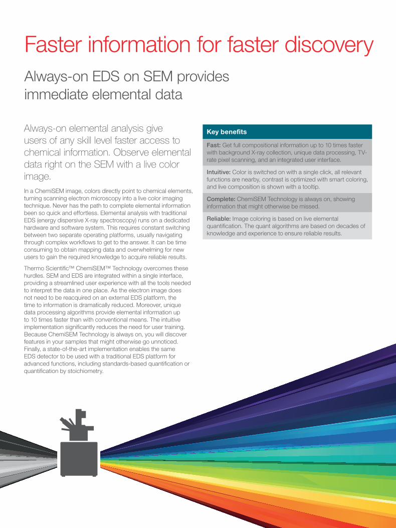
Faster information for faster discovery

Ceramic in glass.
On the cover: Li-ion battery anode
Faster information for faster discovery
Always-on elemental analysis give users of any skill level faster access to chemical information. Observe elemental data right on the SEM with a live color image.In a ChemiSEM image, colors directly point to chemical elements, turning scanning electron microscopy into a live color imaging technique. Never has the path to complete elemental information been so quick and effortless. Elemental analysis with traditional EDS (energy dispersive X-ray spectroscopy) runs on a dedicated hardware and software system. This requires constant switching between two separate operating platforms, usually navigating through complex workflows to get to the answer. It can be time consuming to obtain mapping data and overwhelming for new users to gain the required knowledge to acquire reliable results.
Thermo Scientific™ ChemiSEM™ Technology overcomes these hurdles. SEM and EDS are integrated within a single interface, providing a streamlined user experience with all the tools needed to interpret the data in one place. As the electron image does not need to be reacquired on an external EDS platform, the time to information is dramatically reduced. Moreover, unique data processing algorithms provide elemental information up to 10 times faster than with conventional means. The intuitive implementation significantly reduces the need for user training. Because ChemiSEM Technology is always on, you will discover features in your samples that might otherwise go unnoticed. Finally, a state-of-the-art implementation enables the same EDS detector to be used with a traditional EDS platform for advanced functions, including standards-based quantification or quantification by stoichiometry.
Always-on EDS on SEM provides immediate elemental data
Key benefits
Fast: Get full compositional information up to 10 times faster with background X-ray collection, unique data processing, TV-rate pixel scanning, and an integrated user interface.
Intuitive: Color is switched on with a single click, all relevant functions are nearby, contrast is optimized with smart coloring, and live composition is shown with a tooltip.
Complete: ChemiSEM Technology is always on, showing information that might otherwise be missed.
Reliable: Image coloring is based on live elemental quantification. The quant algorithms are based on decades of knowledge and experience to ensure reliable results.

Live ColorChemiSEM Technology provides live compositional information during routine SEM navigation and imaging. Proprietary electron and X–ray data processing algorithms make ChemiSEM Technology incredibly fast.
Compared to traditional mapping, ChemiSEM Technology will present results much more quickly for the same acquisition parameters, as shown in Figure 1.
Each element is indicated by a different color, so you can clearly see the sample composition in the xT user interface (UI) (Figure 2) without switching to another software program. Each element can be turned on or off in order to focus only on the relevant information.
The color palette can be manually adjusted or automatically refreshed with the SmartColor function. The element selection runs automatically with the AutoID button that provides live identification and user assistance for manual peak identification.
Element identification in live ChemiSEM mode is generated by a quantification algorithm. Therefore, the correct composition is shown, and the results do not suffer from peak overlaps that are typical in gross counts maps. Also, the proprietary shadow detection algorithm assists in providing information only from regions where X-rays are detected (Figure 3).
On-the-fly quantification with the composition tooltipThe tooltip shows the relative concentrations of the sample constituents, making it the quickest way to obtain composition information during live imaging (Figure 4).
Figure 1: Traditional mapping (top) and live ChemiSEM Technology imaging (bottom). Sample: CuNiZn reaction precursor. (20 kV, 0.8 nA, 30 s).
Figure 3: Non-colored area highlighted in red is due to shadowing from a tall feature. Sample: Nickel contamination on a Li-Ion battery anode. (20 kV, 4.5 nA, 90 s).
Figure 4: Live tooltip feature. Sample: silicon oxide and graphite Li-ion battery anode. (15 kV, 1.1 nA).
Figure 2: The dedicated workspace in ChemiSEM Technology is fully integrated in the xT user interface. Sample: Li-Ion battery anode. (15 kV, 1.1 nA).
100 μm
15 μm
15 μm
100 μm

Point analysis and region analysisAccurate quantitative information of a specific point or region of interest can be obtained using Point & ID analyses. These conventional EDS functions are fully integrated in the UI, to enable smooth optimization of the acquisition parameters (such as acquisition time or number of counts). The parameters can also be saved as presets in the user profile. There is no need to acquire a survey scan, because you can work with the image in the UI.
Results obtained from different points or regions can be compared with one click by overlaying their spectra, as shown in Figure 5.
LinescanLinescans can be obtained from any region of the SE or BSE image. As with Point & ID analyses, you can use presets to obtain quick results and switch easily between linescan parameters. Figures 6 and 7 compare results obtained with different parameters.
MappingFor a more conventional approach to elemental analysis, ChemiSEM Technology allows for traditional gross counts mapping. The feature works during live scanning, even with dwell times as short as 100 ns, so slow scanning is not required. Short dwell times make ChemiSEM Technology faster than alternatives, even in this conventional mapping mode, and enable the study of sensitive materials.
With a single click, any combination of elements can be overlaid. Moreover, it is possible to select K, L, and M lines with real-time updates and display (shown in Figure 8).
Figure 5: Point & ID analyses on two areas with different compositions. Spectra obtained from the two acquisitions are overlapped for a qualitative comparison of the peaks. Sample: Al2O3 slag obtained during the steelmaking process. (20 kV, 1.2 nA).
Figure 6: An example of a fast linescan with 10 points per line. Sample: Glass Fiber Reinforced Polymer (GFRP). (20 kV, 1.2 nA).
Figure 7: An example of a finer profiling with 300 points per line. Sample: Complex Inclusion in Steel. (20 kV, 4.5 nA).

ReportingFor fast and easy data reporting, the Job History Manager generates various reports and saves the most important information. For example, you can save the spectrum and quantification (both atomic and weight percentages) for Point & ID analyses, or you can save the quantifications and spectra for each single point of a linescan.
How ChemiSEM Technology worksThe key idea behind the ChemiSEM Technology algorithms is to process the image in segments. ChemiSEM Technology works with an object-based image segmentation and dynamic pixel binning. This means that SE/BSE information is used with X-ray data to give features in the image a color that is based on their composition.
Traditional EDS uses SE/BSE information but does not use image processing, so the data arrives more slowly and the image resolution is relatively coarse. In contrast, ChemiSEM Technology is based on a single-scan generator approach that perfectly aligns the SEM image and EDS image, which produces sharper images and faster results. In addition, new pulse processing with Adaptive Pulse Shaping ensures reliable data acquisition over a range of conditions.
Specifications• Thermo Scientific EDS detector technology and spectral
analysis methodology
• 10, 30, and 60 mm2 detector supported, 129 eV resolution at Mn k-alpha
• Fully integrated EDS in the microscope user interface
• Unprecedented time to data due to tight EDS+SEM integration and on-the-fly spectra acquisition and processing
• Live quantitative EDS mapping down to 100 ns dwell time
• Dynamic pixel binning based on the sample features identified in the SE or BSE image processed by real-time computer vision algorithms
• Dynamic color and shadow detection features
• Live SEM/X-ray elemental map overlay, usable at all scan speeds
• Adaptive Pulse Shaping enables optimal spectral resolution and dead time across a broad range of input count rates
• Automated EDS detector calibrations and on-demand spectral quality validation
• State -of- the- art EDS analytical functions:
– Point and ID
– Region analysis
– Linescan
– Mapping
– Fast and easy data reporting
– Job History Managerr
• Automated peak identification and user assistance for manual peak identification
• On- the- fly quantification that is standardless
• Energy resolution compliant with ISO15632:2002
• Compatible with integrated RGB Cathodoluminescence (CL) detector for simultaneous EDS and CL
EDS Image
ElectronImage
ColorMap
ColorMap
Regular Segments (super pixels)
Object-based Segments
Image Processing
Machine Vision
Figure 10: Proprietary ChemiSEM algorithms ensure sharper images in a shorter amount of time.
Figure 8: Conventional gross counts mapping is available down to 100 ns dwell time per pixel.
20 μm
Figure 9: Example of a report containing different types of analysis.

Applications
Figure 11: Lithium ion battery cathode. (20 kV, 4.5 nA, 90 s).
Figure 13: Ceramic in glass. (20 kV, 4.5 nA, 50 s).
Figure 12: Construction materials. (20 kV, 4.5 nA, 120 s).
100 μm
100 μm
20 μm 20 μm
100 μm
100 μm

For current certifications, visit thermofisher.com/certifications. © 2021 Thermo Fisher Scientific Inc. All rights reserved. All trademarks are the property of Thermo Fisher Scientific and its subsidiaries unless otherwise specified. BR109-EN-08-2021
Find out more at thermofisher.com/ChemiSEM
Figure 15: High resolutions are possible on field emission systems. AuPdPt nanoparticles on TiO2. (10 kV, 1.6 nA, 65 s).
Figure 14: Malachite. (15 kV, 1.1 nA, 120 s).
300 nm 300 nm
25 μm 25 μm


