Issued Date: June 3, 2003 Model No.: V270W1 - L01 Preliminary TFT LCD Preliminary Specification MODEL NO.: V270W1 - L01 1 / 26 The information described in this technical specification is tentative and it is possible to be changed without prior notice. Please contact CMO ’s representative while your product design is based on this specification. Version 1.0
Transcript
Issued Date: June 3, 2003 Model No.: V270W1 - L01
Preliminary
TFT LCD Preliminary Specification
MODEL NO.: V270W1 - L01
1 / 26 The information described in this technical specification is tentative and it is possible to be changed without prior notice. Please contact CMO ’s representative while your product design is based on this specification. Version 1.0
Issued Date: June 3, 2003 Model No.: V270W1 - L01
Preliminary
- CONTENTS -
REVISION HISTORY ------------------------------------------------------- 3 1. GENERAL DESCRIPTION ------------------------------------------------------- 4 1.1 OVERVIEW 1.2 FEATURES 1.3 APPLICATION 1.4 GENERAL SPECIFICATIONS 1.5 MECHANICAL SPECIFICATIONS 2. ABSOLUTE MAXIMUM RATINGS ------------------------------------------------------- 5 2.1 ABSOLUTE RATINGS OF ENVIRONMENT 2.2 ELECTRICAL ABSOLUTE RATINGS 2.2.1 TFT LCD MODULE 2.2.2 BACKLIGHT UNIT 3. ELECTRICAL CHARACTERISTICS ------------------------------------------------------- 6
2 / 26 The information described in this technical specification is tentative and it is possible to be changed without prior notice. Please contact CMO ’s representative while your product design is based on this specification. Version 1.0
Issued Date: June 3, 2003 Model No.: V270W1 - L01
Preliminary
REVISION HISTORY
Version Date Page(New) Section Description
Ver 0.1 Ver 0.2
Ver 1.0
Feb.23, 02 May 02, 03
June 03,03
All 18
19
20
20
21 23
25-2618
25-26
All 7.2
8 9 11 7.2
11
Tentative Specification was second issued. Note(1) Add “Viewing angles are measured by EZ-Contrast 160R (Eldim)” Note(4) The driving signal means the signal of gray level 0,63,127,191,255. Note(7) The LCD module should be stabilized at given temperature for 30 minutes 1hour to avoid abrupt temperature change during measuring. In order to stabilize the luminance, the measurement shouldbe executed after lighting Backlight for 30 minutes 1 hour in a windless room. Note(7) The drawing is updated. Add Packing description Add Label definition The drawing of mechanical characteristics is updated. Min. Typ. Max. Color Chromaticity Green Gx (0.239)(0.269)(0.299) Gy (0.570)(0.600)(0.630)
The drawing of mechanical characteristics is updated.
3 / 26 The information described in this technical specification is tentative and it is possible to be changed without prior notice. Please contact CMO ’s representative while your product design is based on this specification. Version 1.0
Issued Date: June 3, 2003 Model No.: V270W1 - L01
Preliminary
1. GENERAL DESCRIPTION
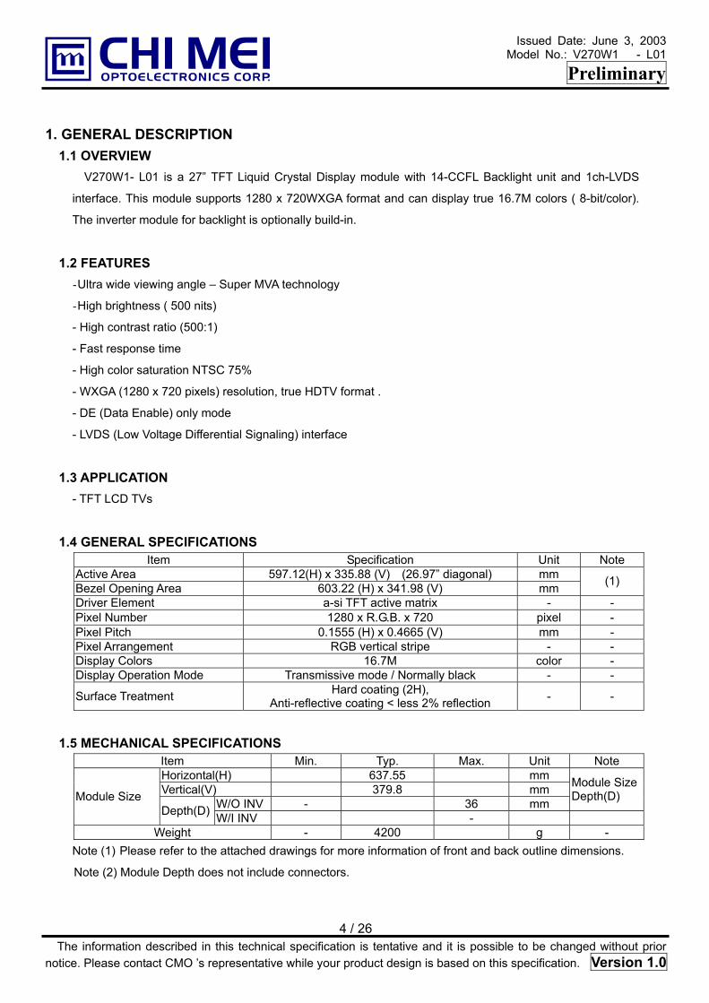
1.1 OVERVIEW V270W1- L01 is a 27” TFT Liquid Crystal Display module with 14-CCFL Backlight unit and 1ch-LVDS
interface. This module supports 1280 x 720WXGA format and can display true 16.7M colors ( 8-bit/color).
The inverter module for backlight is optionally build-in.
1.2 FEATURES - Ultra wide viewing angle – Super MVA technology
- High brightness ( 500 nits)
- High contrast ratio (500:1)
- Fast response time
- High color saturation NTSC 75%
- WXGA (1280 x 720 pixels) resolution, true HDTV format .
- DE (Data Enable) only mode
- LVDS (Low Voltage Differential Signaling) interface
1.3 APPLICATION - TFT LCD TVs
1.4 GENERAL SPECIFICATIONS Item Specification Unit Note
Active Area 597.12(H) x 335.88 (V) (26.97” diagonal) mm Bezel Opening Area 603.22 (H) x 341.98 (V) mm (1)
Driver Element a-si TFT active matrix - - Pixel Number 1280 x R.G.B. x 720 pixel - Pixel Pitch 0.1555 (H) x 0.4665 (V) mm - Pixel Arrangement RGB vertical stripe - - Display Colors 16.7M color - Display Operation Mode Transmissive mode / Normally black - -
Surface Treatment Hard coating (2H), Anti-reflective coating < less 2% reflection - -
1.5 MECHANICAL SPECIFICATIONS Item Min. Typ. Max. Unit Note Horizontal(H) 637.55 mm Vertical(V) 379.8 mm
W/O INV - 36 mm
Module SizeDepth(D) Module Size
Depth(D) W/I INV - Weight - 4200 g -
Note (1) Please refer to the attached drawings for more information of front and back outline dimensions.
Note (2) Module Depth does not include connectors.
4 / 26 The information described in this technical specification is tentative and it is possible to be changed without prior notice. Please contact CMO ’s representative while your product design is based on this specification. Version 1.0
Issued Date: June 3, 2003 Model No.: V270W1 - L01
Preliminary
2. ABSOLUTE MAXIMUM RATINGS 2.1 ABSOLUTE RATINGS OF ENVIRONMENT
Value Item Symbol Min. Max. Unit Note
Storage Temperature TST -20 +60 ºC (1) Operating Ambient Temperature TOP 0 +50 ºC (1), (2) Shock (Non-Operating) SNOP - (100) G (3), (5) Vibration (Non-Operating) VNOP - (1.0) G (4), (5) Note (1) Temperature and relative humidity range is shown in the figure below.
(a) 90 %RH Max. (Ta ≦ 40 ºC).
(b) Wet-bulb temperature should be 39 ºC Max. (Ta > 40 ºC).
(c) No condensation.
Note (2) The temperature of panel display area surface should be 0 ºC Min. and 60 ºC Max.
Note (3) 2 ms, half sine wave, 1 time for ± X, ± Y, ± Z.
Note (4) 10 ~ 500 Hz, 10 min, 1 time each X, Y, Z.
Note (5) At testing Vibration and Shock, the fixture in holding the module has to be hard and rigid enough
so that the module would not be twisted or bent by the fixture.
Storage Range 5
20
60
40
80
-40 -20 0 20 40 60 80
10090
Temperature (ºC)
Operating Range
Relative Humidity (%RH)
5 / 26 The information described in this technical specification is tentative and it is possible to be changed without prior notice. Please contact CMO ’s representative while your product design is based on this specification. Version 1.0
LVDS common input voltage Vic 1.125 1.25 1.375 V Terminating Resistor RT - 100 - ohm Note (1) The module should be always operated within above ranges.
Note (2) Measurement Conditions:
6 / 26 The information described in this technical specification is tentative and it is possible to be changed without prior notice. Please contact CMO ’s representative while your product design is based on this specification. Version 1.0
Issued Date: June 3, 2003 Model No.: V270W1 - L01
Preliminary
+5.0V
(LCD Module Input)FUSE
1uF C3
0.01uF
C247K VR1
1K
R2 2SK1470
Vcc
1uF
C1
Q2
+12V
(High to Low) (Control Signal)
R1 47K
Q1 2SK1475
SW
Vcc rising time is 470µs
0.1Vcc
0.9Vcc
GND
+5V
470µs
Note (3) The specified power supply current is under the conditions at Vcc = 5 V, Ta = 25 ± 2 ºC, fv = 60 Hz,
whereas a power dissipation check pattern below is displayed.
b. Black Pattern a. White Pattern
Active Area Active Area
7 / 26 The information described in this technical specification is tentative and it is possible to be changed without prior notice. Please contact CMO ’s representative while your product design is based on this specification. Version 1.0
Issued Date: June 3, 2003 Model No.: V270W1 - L01
Preliminary
R
R
R
B
B
B
B
G
G
G
G
B
B
B
B
B
B
G
G
G
G
R
R
R R
R
R
R
c. Vertical Stripe Pattern
Active Area
3.2 BACKLIGHT UNIT Ta = 25 ± 2 ºC Value Parameter Symbol Min. Typ. Max. Unit Note
Lamp Input Voltage VL 1008 1120 1232 VRMS IL = (4.65) mA Lamp Current IL 4.35 4.65 4.95 mARMS (1)
1200 - 3000 VRMS (2), Ta = 25 ºC Lamp Turn On Voltage VS 1790 - 3000 VRMS (2), Ta = 0 ºC Operating Frequency FL 50 55 60 KHz (3) Lamp Life Time LBL 50K - - Hrs (5) Power Consumption PL - 90 - W (4), IL = (4.65) mANote (1) Lamp current is measured by utilizing high frequency current meters as shown below:
Inverter
1HV (Pink)
2HV (White)
1HV (Pink)
2HV (White)
1HV (Pink)
2HV (White)
1HV (Pink)
2HV (White)
1HV (Pink)
2HV (White)
1HV (Pink)
2HV (White)
1HV (Pink)
2HV (White)
A A A A A A A A A A A A A A
8 / 26 The information described in this technical specification is tentative and it is possible to be changed withounotice. Please contact CMO ’s representative while your product design is based on this specification. Versio
LCD Module
LV (Gray)
t prior n 1.0
Issued Date: June 3, 2003 Model No.: V270W1 - L01
Preliminary
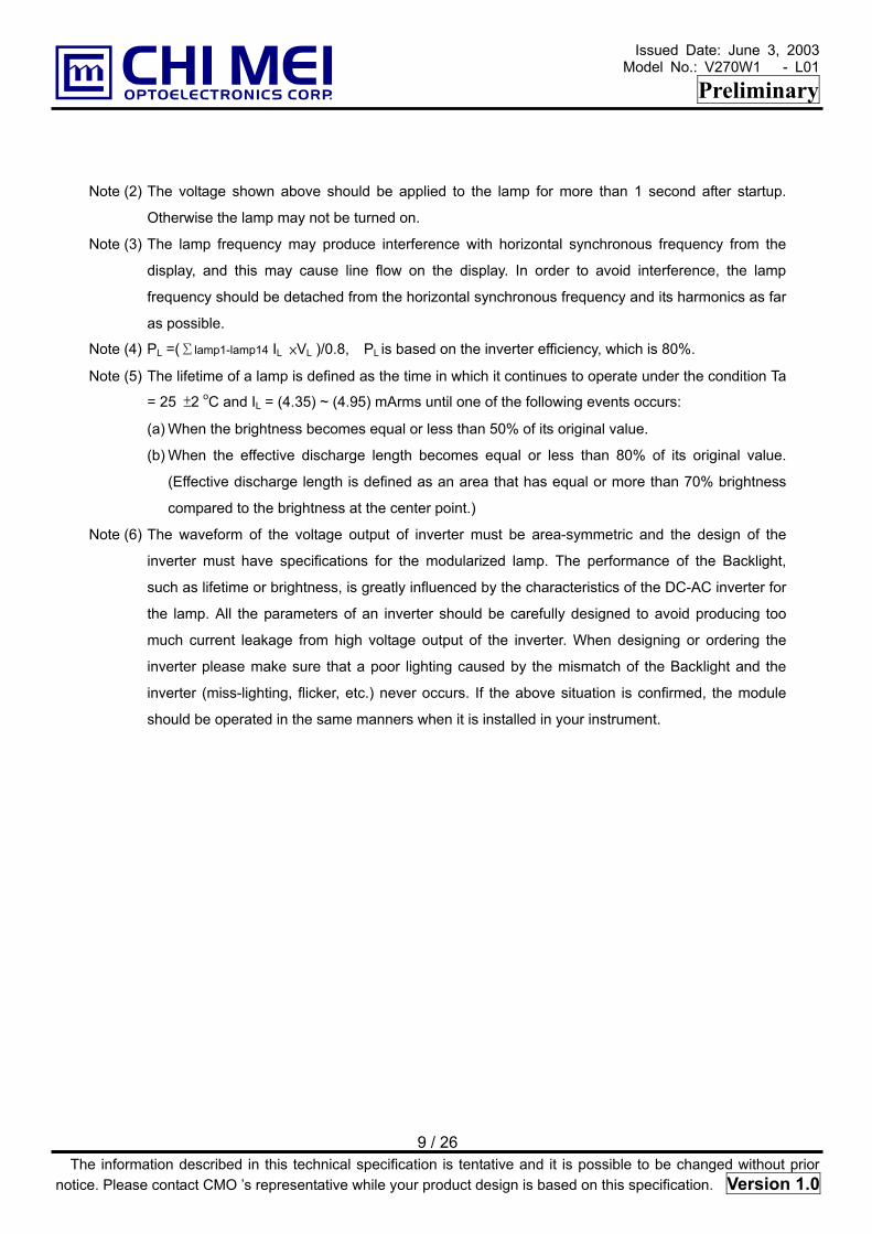
Note (2) The voltage shown above should be applied to the lamp for more than 1 second after startup.
Otherwise the lamp may not be turned on.
Note (3) The lamp frequency may produce interference with horizontal synchronous frequency from the
display, and this may cause line flow on the display. In order to avoid interference, the lamp
frequency should be detached from the horizontal synchronous frequency and its harmonics as far
as possible.
Note (4) PL =(Σlamp1-lamp14 IL ×VL )/0.8, PL is based on the inverter efficiency, which is 80%.
Note (5) The lifetime of a lamp is defined as the time in which it continues to operate under the condition Ta
= 25 ±2 oC and IL = (4.35) ~ (4.95) mArms until one of the following events occurs:
(a) When the brightness becomes equal or less than 50% of its original value.
(b) When the effective discharge length becomes equal or less than 80% of its original value.
(Effective discharge length is defined as an area that has equal or more than 70% brightness
compared to the brightness at the center point.)
Note (6) The waveform of the voltage output of inverter must be area-symmetric and the design of the
inverter must have specifications for the modularized lamp. The performance of the Backlight,
such as lifetime or brightness, is greatly influenced by the characteristics of the DC-AC inverter for
the lamp. All the parameters of an inverter should be carefully designed to avoid producing too
much current leakage from high voltage output of the inverter. When designing or ordering the
inverter please make sure that a poor lighting caused by the mismatch of the Backlight and the
inverter (miss-lighting, flicker, etc.) never occurs. If the above situation is confirmed, the module
should be operated in the same manners when it is installed in your instrument.
9 / 26 The information described in this technical specification is tentative and it is possible to be changed without prior notice. Please contact CMO ’s representative while your product design is based on this specification. Version 1.0
Issued Date: June 3, 2003 Model No.: V270W1 - L01
Preliminary
4. BLOCK DIAGRAM 4.1 TFT LCD MODULE
TFT LCD PANEL
(1280x3x720)
DATA DRIVER IC
SCA
N D
RIVER
IC
LVDS INPUT /
OVER DRIVING CONTROLLER /
TIMING CONTROLLER
I
NPU
T CO
NN
ECTO
R(JA
E-FI-SE30P-HF)
LAMP CONNECTO
Vcc
VL
4.2 BACKLIGHT UNIT Lamp connector
HV : BHR-03-VS-1(JST) *7
LV : ZHR-2 (JST) *1
The information described in this technotice. Please contact CMO ’s represent
DC/DC CONVERTER &
REFERENCE VOLTAGE
GND
RX0(+/-)
RX1(+/-)
RX2(+/-)
RX3(+/-)
RXC(+/-)
BACKLIGHT UNITR
1 LV(Gray)
1 HV(Pink)
2 HV(White)
2 HV(White)
1 HV(Pink)
2 HV(White)
10 / 26 nical specification is tentative and it is possible to be changed without prior ative while your product design is based on this specification. Version 1.0
Issued Date: June 3, 2003 Model No.: V270W1 - L01
Preliminary
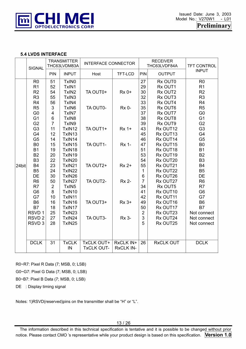
5. INPUT TERMINAL PIN ASSIGNMENT
5.1 TFT LCD MODULE Pin Name Description 1 NC No Connection 2 NC No Connection 3 NC No Connection 4 NC No Connection 5 NC No Connection 6 NC No Connection 7 NC No Connection 8 GND Ground 9 RX3+ Positive LVDS differential data input. Channel 3
5.2 BACKLIGHT UNIT Pin Symbol Description Color 1 HV High Voltage Pink 2 HV High Voltage White
Note (1) Connector Part No.: BHR-03VS-1 (JST) or equivalent
Note (2) User’s connector Part No.: SM02(8.0)B-BHS-1TB (JST) or equivalent
Pin Symbol Description Color 1 LV Low Voltage Gray 2 NC No Connection
Note (1) Connector Part No.: ZHR-2 (JST) or equivalent
11 / 26 The information described in this technical specification is tentative and it is possible to be changed without prior notice. Please contact CMO ’s representative while your product design is based on this specification. Version 1.0
Issued Date: June 3, 2003 Model No.: V270W1 - L01
Preliminary
Note (2) User’s connector Part No.: S2B-ZR-SM3A-TF (JST) or equivalent
5.3 BLOCK DIAGRAM OF INTERFACE
CNF1
100pF
R0~R7
G0~G7
B0~B7
DE
Notes: 1)
2)
The informnotice. Pleas
R0-R7
100pF7 7
G0-G
e
B0-B7
100pF
Th
LV
us
ati c
DE
Rx3+
100pF
00pF
Host Graphics Controller
: Pixel
: Pixel
: Pixel
: Displ
e syste
DS ca
ed diffe
on desontact
TxIN
R Data
G Data
B Data
ay timing s
m must h
ble impeda
rentially.
cribed in tCMO ’s re
PLL
ignal
ave the transmitter to drive the module.
nce shall be 50 ohms per signal line or abou
12 / 26 his technical specification is tentative and itpresentative while your product design is bas
Notes: 1)RSVD(reserved)pins on the transmitter shall be “H” or “L”.
13 / 26 The information described in this technical specification is tentative and it is possible to be changed without prior notice. Please contact CMO ’s representative while your product design is based on this specification. Version 1.0
Issued Date: June 3, 2003 Model No.: V270W1 - L01
Preliminary
5.5 COLOR DATA INPUT ASSIGNMENT The brightness of each primary color (red, green and blue) is based on the 8-bit gray scale data input for
the color. The higher the binary input, the brighter the color. The table below provides the assignment of
color versus data input. Data Signal
Red Green Blue Color R7 R6 R5 R4 R3 R2 R1 R0 R7 R6 G5 G4 G3 G2 G1 G0 R7 R6 B5 B4 B3 B2 B1 B0
Basic Colors
Black Red Green Blue Cyan Magenta Yellow White
01000111
0 1 0 0 0 1 1 1
0 1 0 0 0 1 1 1
0 1 0 0 0 1 1 1
01000111
01000111
01000111
01000111
00101011
00101011
00101011
00101011
00101011
00101011
00101011
0 0 1 0 1 0 1 1
0 0 0 1 1 1 0 1
0 0 0 1 1 1 0 1
0 0 0 1 1 1 0 1
0 0 0 1 1 1 0 1
00011101
00011101
00011101
00011101
Gray Scale Of Red
Red(0) / Dark Red(1) Red(2)
: :
Red(253) Red(254) Red(255)
000::111
0 0 0 : : 1 1 1
0 0 0 : : 1 1 1
0 0 0 : : 1 1 1
000::111
000::111
001::011
010::101
000::000
000::000
000::000
000::000
000::000
000::000
000::000
0 0 0 : : 0 0 0
0 0 0 : : 0 0 0
0 0 0 : : 0 0 0
0 0 0 : : 0 0 0
0 0 0 : : 0 0 0
000::000
000::000
000::000
000::000
Gray Scale Of Green
Green(0) / Dark Green(1) Green(2)
: :
Green(253) Green(254) Green(255)
000::000
0 0 0 : : 0 0 0
0 0 0 : : 0 0 0
0 0 0 : : 0 0 0
000::000
000::000
000::000
000::000
000::111
000::111
000::111
000::111
000::111
000::111
001::011
0 1 0 : : 1 0 1
0 0 0 : : 0 0 0
0 0 0 : : 0 0 0
0 0 0 : : 0 0 0
0 0 0 : : 0 0 0
000::000
000::000
000::000
000::000
Gray Scale Of Blue
Blue(0) / Dark Blue(1) Blue(2)
: :
Blue(253) Blue(254) Blue(255)
000::000
0 0 0 : : 0 0 0
0 0 0 : : 0 0 0
0 0 0 : : 0 0 0
000::000
000::000
000::000
000::000
000::000
000::000
000::000
000::000
000::000
000::000
000::000
0 0 0 : : 0 0 0
0 0 0 : : 1 1 1
0 0 0 : : 1 1 1
0 0 0 : : 1 1 1
0 0 0 : : 1 1 1
000::111
000::111
001::011
010::101
Note (1) 0: Low Level Voltage, 1: High Level Voltage
14 / 26 The information described in this technical specification is tentative and it is possible to be changed without prior notice. Please contact CMO ’s representative while your product design is based on this specification. Version 1.0
Issued Date: June 3, 2003 Model No.: V270W1 - L01
Preliminary
6. INTERFACE TIMING
6.1 INPUT SIGNAL TIMING SPECIFICATIONS The input signal timing specifications are shown as the following table and timing diagram.
Signal Item Symbol Min. Typ. Max. Unit Note Clock Frequency 1/Tc (70) 74.25 80 MHZ -
Frame Rate Fr 48 60 - Hz Tv=Tvd+TvbTotal Tv 730 750 850 Th - Display Tvd 720 720 720 Th - Vertical Active Display Term
Note: Because of this module is operated by DE only mode, Hsync and Vsync input signals should be set
to low logic level or ground. Otherwise, this module would operate abnormally.
INPUT SIGNAL TIMING DIAGRAM
DATA
DE
Thd
DCLK
Tc
Valid display data (1280 clocks)
Thb
DE
Th
Tv
Tvb Tvd
15 / 26 The information described in this technical specification is tentative and it is possible to be changed without prior notice. Please contact CMO ’s representative while your product design is based on this specification. Version 1.0
Issued Date: June 3, 2003 Model No.: V270W1 - L01
Preliminary
6.2 POWER ON/OFF SEQUENCE To prevent a latch-up or DC operation of LCD module, the power on/off sequence should be as the diagram below.
0≦T1≦10ms 0≦T2≦50ms 0≦T3≦50ms 1s≦T4
50%
0V
0V
50%
T6 T5
T3 T1
0.1VDD
0.9 VCC
0.1VCC
0.9 VCC
T4 T2
VALID
Power On
Power Supply
VCC
Signals
Power Off
Backlight (Recommended) 450ms≦T5 100ms≦T6
Power ON/OFF Sequence
Note.
(1) The supply voltage of the external system for the module input should be the same as the definition of Vcc.
(2) Apply the lamp voltage within the LCD operation range. When the backlight turns on before the LCD operation of
the LCD turns off before the backlight turns off, the display may momentarily become abnormal screen.
(3) In case of VCC = off level, please keep the level of input signals on the low or keep a high impedance.
(4) T4 should be measured after the module has been fully discharged between power of and on period.
(5) Interface signal shall not be kept at high impedance when the power is on.
16 / 26 The information described in this technical specification is tentative and it is possible to be changed without prior notice. Please contact CMO ’s representative while your product design is based on this specification. Version 1.0
Issued Date: June 3, 2003 Model No.: V270W1 - L01
Preliminary
7. OPTICAL CHARACTERISTICS 7.1 TEST CONDITIONS
Item Symbol Value Unit Ambient Temperature Ta 25±2 oC Ambient Humidity Ha 50±10 %RH Supply Voltage VCC 5.0 V Input Signal According to typical value in "3. ELECTRICAL CHARACTERISTICS" Inverter Current IL (4.65) mA Inverter Driving Frequency FL 55 KHz Inverter --
7.2 OPTICAL SPECIFICATIONS
The relative measurement methods of optical characteristics are shown in 7.2. The following items should
be measured under the test conditions described in 7.1 and stable environment shown in Note (7). Item Symbol Condition Min. Typ. Max. Unit Note
Contrast Ratio CR - (500) - - Note(2) TR - (15) - ms TF - (10) - ms
Note(3) Response Time
Gray to gray (16.6) ms Note(4)
Center Luminance of White LC (450) (500) - cd/m2 Note(5) Average Luminance of White LAVE (400) (450) - cd/m2 White Variation δW - - 1.6 - Note(8) Cross Talk CT - - 4.0 % Note(6)
Rx (0.616) (0.646) (0.676) - Red Ry (0.302) (0.332) (0.362) - Gx (0.239) (0.269) (0.299) - Green Gy (0.570) (0.600) (0.630) - Bx (0.112) (0.142) (0.172) - Blue By (0.042) (0.072) (0.102) -
Wx 0.255 0.285 0.315 -
Color Chromaticity
White Wy
θx=0°, θY =0° Viewing Normal Angle
0.263 0.293 0.323 - 9, 300K
θx+ (85) - Horizontal θx- (85) - θY+ (85) -
Viewing Angle
Vertical θY-
CR≥10
(85) -
Deg. No gray
scale inversion
17 / 26 The information described in this technical specification is tentative and it is possible to be changed without prior notice. Please contact CMO ’s representative while your product design is based on this specification. Version 1.0
Issued Date: June 3, 2003 Model No.: V270W1 - L01
Preliminary
18 / 26 The information described in this technical specification is tentative and it is possible to be changed without prior notice. Please contact CMO ’s representative while your product design is based on this specification. Version 1.0
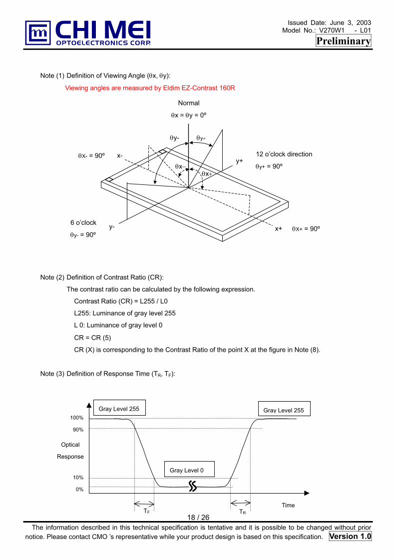
Note (1) Definition of Viewing Angle (θx, θy):
Viewing angles are measured by Eldim EZ-Contrast 160R
θX- = 90º
θX+ = 90º
Normal
θx = θy = 0º
x+ y-
y+x-
θy+ θy-
θx+ θx−
6 o’clock
θy- = 90º
12 o’clock direction
θy+ = 90º
Note (2) Definition of Contrast Ratio (CR):
The contrast ratio can be calculated by the following expression.
Contrast Ratio (CR) = L255 / L0
L255: Luminance of gray level 255
L 0: Luminance of gray level 0
CR = CR (5)
CR (X) is corresponding to the Contrast Ratio of the point X at the figure in Note (8).
Note (3) Definition of Response Time (TR, TF):
Gray Level 255 Gray Level 255
Optical
Response
100%
90%
10%
0%
Gray Level 0
Time TF TR
Issued Date: June 3, 2003 Model No.: V270W1 - L01
Preliminary
Note (4) Definition of Gray to Gray Switching Time:
Optical
Response
100%90%
10%0%
Gray to gray switching time
Time
Time Gray to gray switching time
Drive signal
of LCD Panel
The driving signal means the signal of gray level 0,63,127,191,255.
Note (5) Definition of Luminance of White (LC, LAVE):
Measure the luminance of gray level 255 at center point and 5 points
LC = L (5)
LAVE = [L (1)+ L (2)+ L (3)+ L (4)+ L (5)] / 5
L (x) is corresponding to the luminance of the point X at the figure in Note (8).
Note (6) Definition of Cross Talk (CT):
CT = | YB – YA | / YA × 100 (%)
Where:
YA = Luminance of measured location without gray level 0 pattern (cd/m2)
YB = Luminance of measured location with gray level 0 pattern (cd/m2)
(0, 0)
YA, L (D/8,W/2)
YA, D (D/2,7W/8)
a a
The information describnotice. Please contact CMO
Active Are
Gray 128
YA, U (D/2,W/8) YB, U (D/2,W/8)
0
(D/4,W/4)
YB, R (7D/8,W/2)YB, L (D/8,W/2)
ed in this technica ’s representative
YA, R (7D/8,W/2)(3D/4,3W/4)
YB, D (D/2,7W/8)
(D,W)
19 / 26 l specification is tentative and it i while your product design is base
Active Are
s d
Gray Gray
(0, 0)
possible to be ch on this specificati
Gray 128
0
(D,W)
anged without prior on. Version 1.0
Issued Date: June 3, 2003 Model No.: V270W1 - L01
Preliminary
Note (7) Measurement Setup:
The LCD module should be stabilized at given temperature for 1hour to avoid abrupt
temperature change during measuring. In order to stabilize the luminance, the measurement
should be executed after lighting Backlight for 1 hour in a windless room.
Light Shield Room
(Ambient Luminance < 2 lux)
Display Color Analyzer (Minolta CA210)
Center of the Screen
LCD Panel
LCD Module
Note (8) Definition of White Variation (δW):
Measure the luminance of gray level 255 at 5 points
δW = Maximum [L (1), L (2), L (3), L (4), L (5)] / Minimum [L (1), L (2), L (3), L (4), L (5)]
Horizontal Line
X
3W/4
W/2
W/4
3D/4D/2D/4
43
21
5 : Test Point
X=1 to 5 W
D
Verti
cal L
ine
Active Area
20 / 26 The information described in this technical specification is tentative and it is possible to be changed without prior notice. Please contact CMO ’s representative while your product design is based on this specification. Version 1.0
Issued Date: June 3, 2003 Model No.: V270W1 - L01
Preliminary
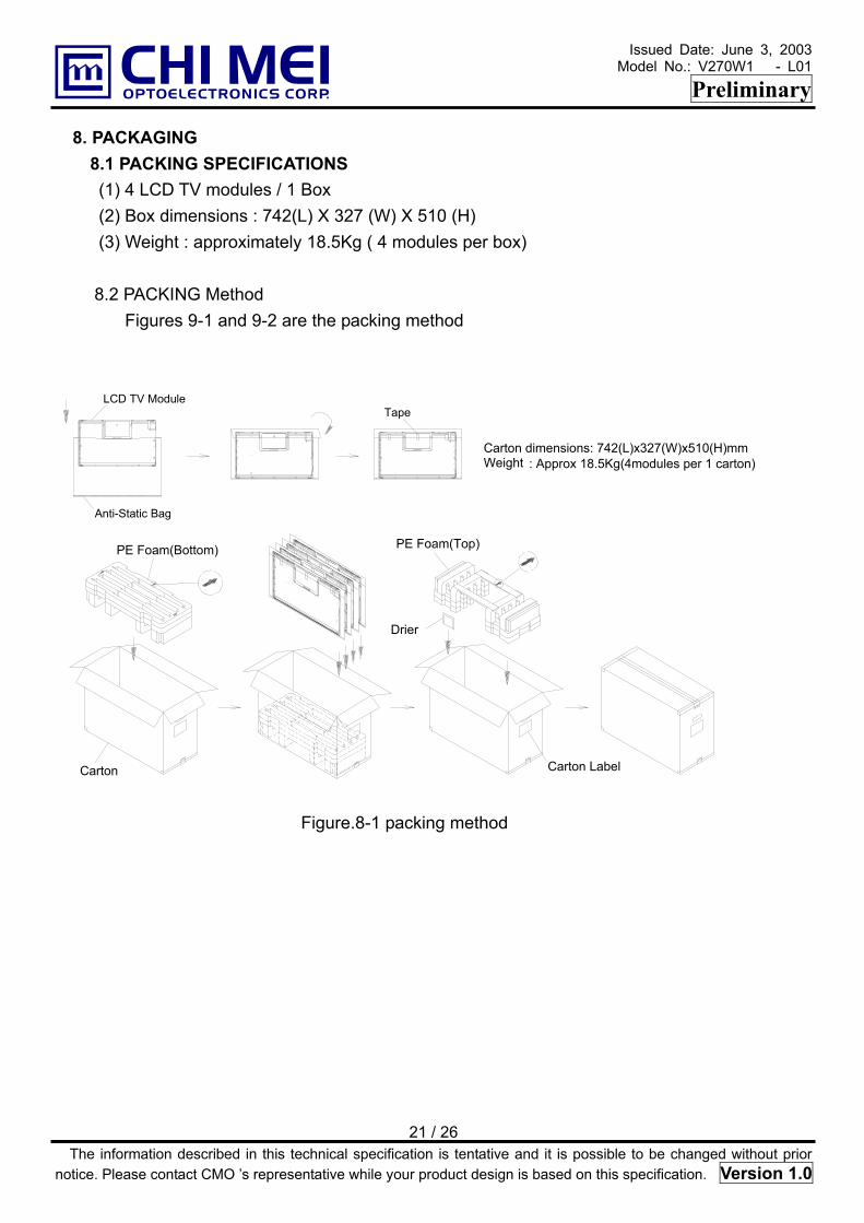
8. PACKAGING 8.1 PACKING SPECIFICATIONS
(1) 4 LCD TV modules / 1 Box (2) Box dimensions : 742(L) X 327 (W) X 510 (H) (3) Weight : approximately 18.5Kg ( 4 modules per box) 8.2 PACKING Method Figures 9-1 and 9-2 are the packing method
LCD TV Module
Anti-Static Bag
Drier
Carton Label
: Approx 18.5Kg(4modules per 1 carton)Carton dimensions: 742(L)x327(W)x510(H)mmWeight
Carton
PE Foam(Bottom)
Tape
Figure.8-1 packing method
21 / 26 The information described in this technical specification is tentative and it is possible to be changed without prior notice. Please contact CMO ’s representative while your product design is based on this specification. Version 1.0
22 / 26 The information described in this technical specification is tentative and it is possible to be changed without prior notice. Please contact CMO ’s representative while your product design is based on this specification. Version 1.0
Issued Date: June 3, 2003 Model No.: V270W1 - L01
Preliminary
9. DEFINITION OF LABELS 9.1 CMO MODULE LABEL
The barcode nameplate is pasted on each module as illustration, and its definitions are as following explanation.
(a) Model Name: V270W1-L01
(b) Revision: Rev. XX, for example: A0, A1… B1, B2… or C1, C2…etc.
(c) Serial ID: X X X X X X X Y M D L N N N N
Product Line
Year, Month, Date
Serial No.
CHI MEI OPTOELECTRONICS MADE IN TAIWAN
E207943
X X X X X X X Y M D L N N N N
MADE IN TAIWAN V270W1 -L01 Rev. XX
CMO Internal Use
CMO Internal Use
Revision
CMO Internal Use Serial ID includes the information as below:
(a) Manufactured Date: Year: 1~9, for 2000~2009
Month: 1~9, A~C, for Jan. ~ Dec.
Day: 1~9, A~Y, for 1st to 31st, exclude I ,O, and U.
(b) Revision Code: Cover all the change
(c) Serial No.: Manufacturing sequence of product
(d) Product Line: 1 -> Line1, 2 -> Line 2, …etc.
23 / 26 The information described in this technical specification is tentative and it is possible to be changed without prior notice. Please contact CMO ’s representative while your product design is based on this specification. Version 1.0
Issued Date: June 3, 2003 Model No.: V270W1 - L01
Preliminary
10. PRECAUTIONS 10.1 ASSEMBLY AND HANDLING PRECAUTIONS
(1) Do not apply rough force such as bending or twisting to the module during assembly.
(2) It is recommended to assemble or to install a module into the user’s system in clean working areas.
The dust and oil may cause electrical short or worsen the polarizer.
(3) Do not apply pressure or impulse to the module to prevent the damage of LCD panel and Backlight.
(4) Always follow the correct power-on sequence when the LCD module is turned on. This can prevent the
damage and latch-up of the CMOS LSI chips.
(5) Do not plug in or pull out the I/F connector while the module is in operation.
(6) Do not disassemble the module.
(7) Use a soft dry cloth without chemicals for cleaning, because the surface of polarizer is very soft and
easily scratched.
(8) Moisture can easily penetrate into LCD module and may cause the damage during operation.
(9) High temperature or humidity may deteriorate the performance of LCD module. Please store LCD
modules in the specified storage conditions.
(10) When ambient temperature is lower than 10ºC, the display quality might be reduced. For example, the
response time will become slow, and the starting voltage of CCFL will be higher than that of room
temperature.
10.2 SAFETY PRECAUTIONS (1) The startup voltage of a Backlight is approximately 1000 Volts. It may cause an electrical shock while
assembling with the inverter. Do not disassemble the module or insert anything into the Backlight unit.
(2) If the liquid crystal material leaks from the panel, it should be kept away from the eyes or mouth. In
case of contact with hands, skin or clothes, it has to be washed away thoroughly with soap.
(3) After the module’s end of life, it is not harmful in case of normal operation and storage.
24 / 26 The information described in this technical specification is tentative and it is possible to be changed without prior notice. Please contact CMO ’s representative while your product design is based on this specification. Version 1.0
Issued Date: June 3, 2003 Model No.: V270W1 - L01
Preliminary
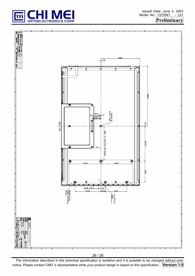
11. MECHANICAL CHARACTERISTICS
25 / 26 The information described in this technical specification is tentative and it is possible to be changed without prior notice. Please contact CMO ’s representative while your product design is based on this specification. Version 1.0
Issued Date: June 3, 2003 Model No.: V270W1 - L01
Preliminary
26 / 26
The information described in this technical specification is tentative and it is possible to be changed without prior notice. Please contact CMO ’s representative while your product design is based on this specification. Version 1.0