21
Chip IO Prof. MacDonald

Chip IO
Prof. MacDonald
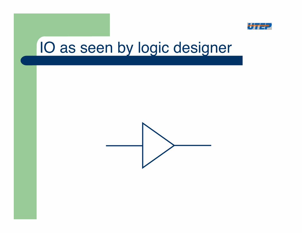
IO as seen by logic designer!
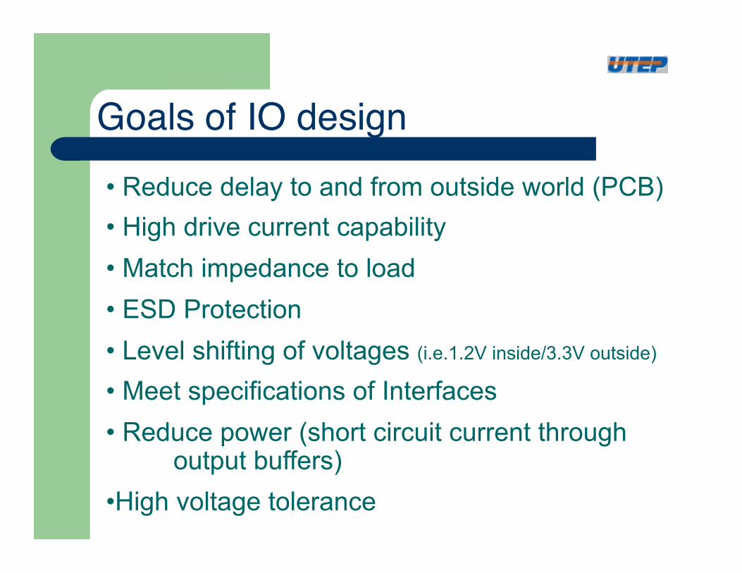
Goals of IO design!• Reduce delay to and from outside world (PCB) • High drive current capability • Match impedance to load • ESD Protection • Level shifting of voltages (i.e.1.2V inside/3.3V outside)
• Meet specifications of Interfaces • Reduce power (short circuit current through
output buffers) • High voltage tolerance

IO Cells and Placement!
Wirebond IO

Interface signaling standards!• Single ended vs. Differential • Levels – Voh, Vol, Vih, Vil • Termination • Most common Interfaces
• TTL is old school – Transistor-Transistor Logic • term used generically for 5V single-ended logic • not really used for last 25 years
• CMOS and LVCMOS • 5V, 3.3V, 2.5V, 1.8V, 1.5V and 1.2V (technology driven) • Vil ~ 0.8V, • Vih ~ .75*Vdd
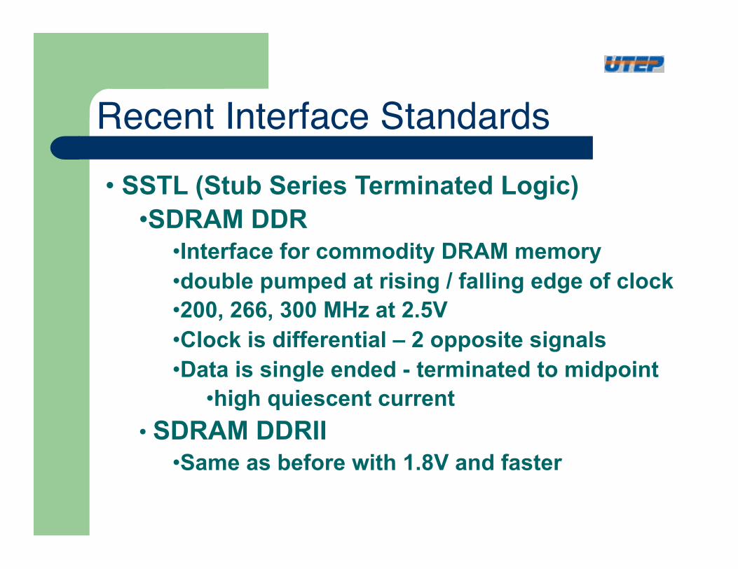
Recent Interface Standards!• SSTL (Stub Series Terminated Logic)
• SDRAM DDR • Interface for commodity DRAM memory • double pumped at rising / falling edge of clock • 200, 266, 300 MHz at 2.5V • Clock is differential – 2 opposite signals • Data is single ended - terminated to midpoint
• high quiescent current • SDRAM DDRII
• Same as before with 1.8V and faster

SSTL!

Recent Interface Standards!• LVDS (Low Voltage Differential Signaling)
• Used for really high speed operation (500MHz <) • Example: 200 MSPS 12bit ADC
• Data is sent in pairs that run +/- 0.35 from midpoint • Differential mode improves noise sensitivity
• noise affects both lines and is cancelled out • reduce voltage swing improves speed • reduce voltage swing improves dynamic power
• but termination cause hugh static power • Base for many competing serial interconnects
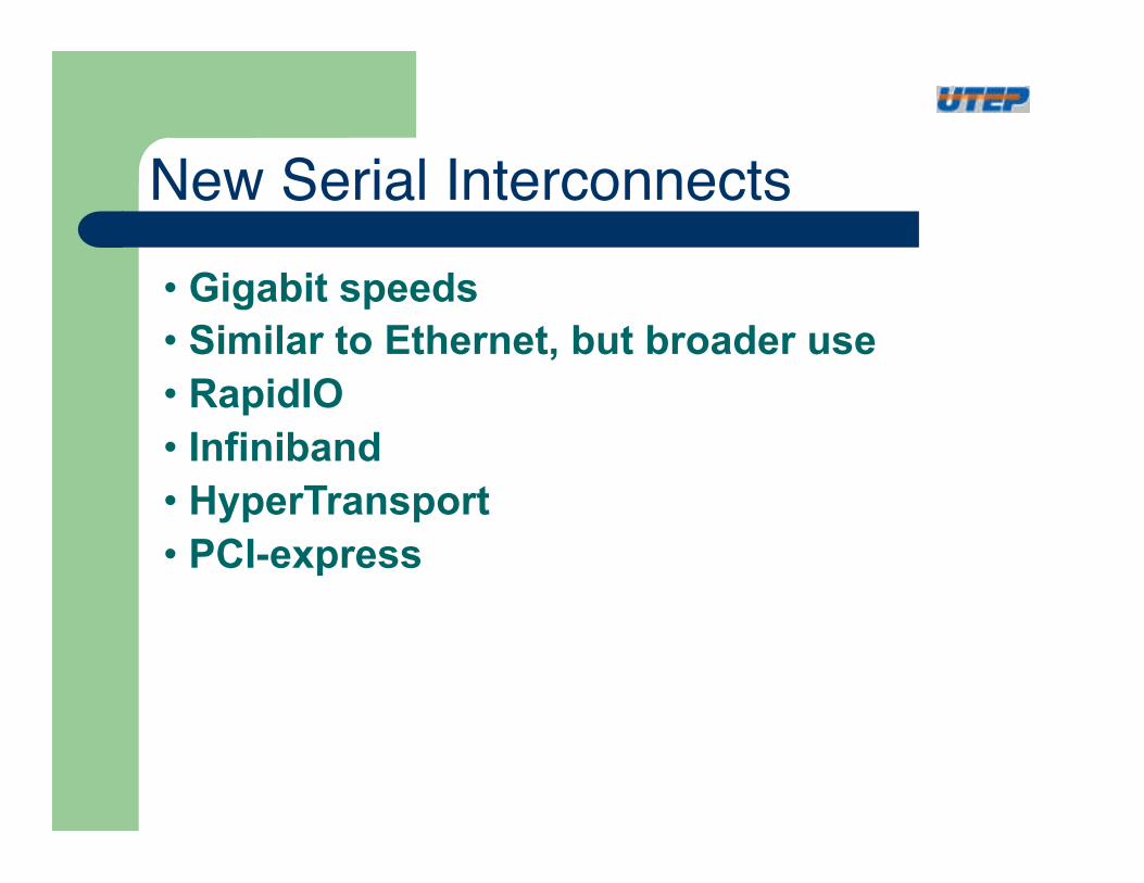
New Serial Interconnects!• Gigabit speeds • Similar to Ethernet, but broader use • RapidIO • Infiniband • HyperTransport • PCI-express

IO Libraries - Artisan TSMC!Cell Name Description PCI33DGZ 3-STATE OUTPUT PCI BUFFER PAD WITH INPUT AND LIMITED SLEW RATE, 5V-Tolerant PCI66DGZ 3-STATE OUTPUT PCI BUFFER PAD WITH INPUT AND LIMITED SLEW RATE, 5V-Tolerant PDBxDGZ CMOS 3-State Output Pad with Input, 5V-Tolerant PDDDGZ Input Pad With Pulldown, 5-VT IO PDDSDGZ Schmitt Trigger Input Pad, 5V-Tolerant PDDxDGZ CMOS 3-State Output Pad with Input and Pulldown, 5V-Tolerant PDIDGZ Input Pad, 5V-Tolerant PDISDGZ Schmitt Trigger Input Pad, 5V-Tolerant PDOxCDG CMOS Output Pad PDTxDGZ CMOS 3-State Output Pad, 5V-Tolerant PDUDGZ Input Pad With Pullup, 5V-Tolerant PDUSDGZ Schmitt Trigger Input Pad, 5V-Tolerant PDUxDGZ CMOS 3-State Output Pad with Input and Pullup, 5V-Tolerant PDXOExDG Crystal Oscillator with High Enable PDXOxDG Crystal Oscillator PRBxDGZ CMOS 3-State Output Pad with Input and Limited Slew Rate, 5V-Tolerant PRDxDGZ CMOS 3-State Output Pad with Input, Pulldown, and Limited Slew Rate, 5V-Tolerant PROxCDG CMOS Output Pad with Limited Slew Rate PRTxDGZ CMOS 3-State Output Pad with Limited Slew Rate, 5V-Tolerant PRUxDGZ CMOS 3-State Output Pad with Input, Pullup, and Limited Slew Rate, 5V-Tolerant PVDDxDGZ Vdd Pad PVSSxDGZ Vss Pad

IO Libraries - Artisan TSMC!Truth Table INPUT OUTPUT OEN I PAD C 1 x 0 0 1 x 1 1 1 x Z 0 0 0 0 0 0 1 1 1 Cell Information Cell Name No. Pad Req. Power (uW/MHz) Drive Capability (mA) PDD02DGZ 1 99.97 2.00 PDD04DGZ 1 56.97 4.00 PDD24DGZ 1 82.90 24.00 Pin Capacitance (pF) Cell Name C I OEN PAD PDD02DGZ 0.046 0.106 0.060 5.435 PDD04DGZ 0.046 0.107 0.060 5.454 PDD24DGZ 0.046 0.114 0.068 5.141 Propagation Delays (ns)
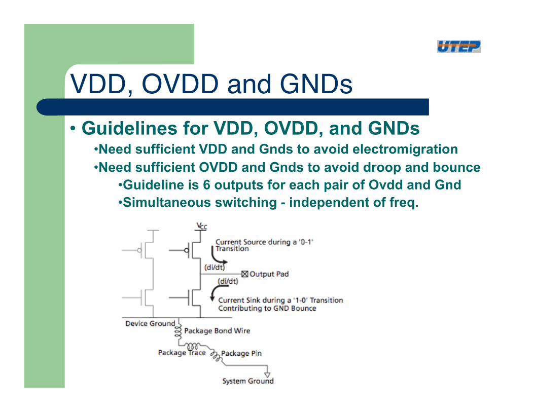
VDD, OVDD and GNDs!!• Guidelines for VDD, OVDD, and GNDs
• Need sufficient VDD and Gnds to avoid electromigration • Need sufficient OVDD and Gnds to avoid droop and bounce
• Guideline is 6 outputs for each pair of Ovdd and Gnd • Simultaneous switching - independent of freq.
Simultaneous Switching!• Consider a 64 bit output bus • If all transition from high to low, • lots of current must be sunk by gnd • Voltage drop will develop from gndi and gnde • Extent can be measured on quiet low output • Problem is independent of frequency • Causes compression of supply voltage and thus results in unexpected slow down.
Simultaneous Switching!• Identify SS IO and spread them out • Avoid placing near asynch inputs • Can use low slew IO - but performance suffers • Stagger timing of outputs • At most 6 outputs per power pin pair • 3 outputs per power pin is rock solid • Add decoupling caps between Ovdd and Gnd • Decrease cap load on outputs

Design of basic CMOS IO!• Output buffer must be very large
• needs to drive pF not fF – 1000’s time larger than normal • presents huge load to internal logic
• so requires increasing fanout inverter chain to be driven • short circuit current is unacceptable
• so pullup/pulldown must be mutually exclusive
2000u
1000u
time
nfet_enable
pfet_enableN
bondpad
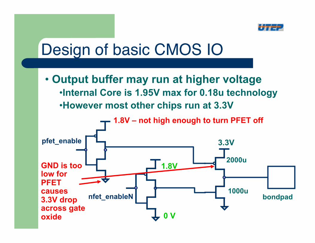
Design of basic CMOS IO!• Output buffer may run at higher voltage
• Internal Core is 1.95V max for 0.18u technology • However most other chips run at 3.3V
2000u
1000u bondpad
3.3V
1.8V – not high enough to turn PFET off
1.8V
nfet_enableN
pfet_enable
GND is too low for PFET causes 3.3V drop across gate oxide 0 V

Input Buffers!
bondpad
50u
25u
1.8V
25u
1.8V 3.3V or 0V
• Input buffer drives internal logic • General much smaller than output buffer • May need to downshift signal voltage with 0Vt device
0vt

ESD protection!• Static discharge is like a grenade to dainty
CMOS transistors • cause gate oxide to rupture • permanent damage to chips
• Three models • human body model (low energy – high voltage – 2kV typical) • machine body model (higher energy) • charge body model (another model – can’t remember)
• All CMOS chips are tested as a part of reliability studies to measure ESD levels that can be withstood.

ESD protection!
bondpad
50u
25u
1.8V
25u
1.8V +/- 2kV
1.8V
• If bond pad exceeds Vdd + diode drop, top diode turns on and discharges static • If bond pad drops below one diode drop below ground, bottom diode turns on • In either case, the gate oxide of the input buffer is protected.

IO circuit with level shifters !

Level Shifters!


