4.3 Thermal Measurement Method in Module --------------------------------------- 48
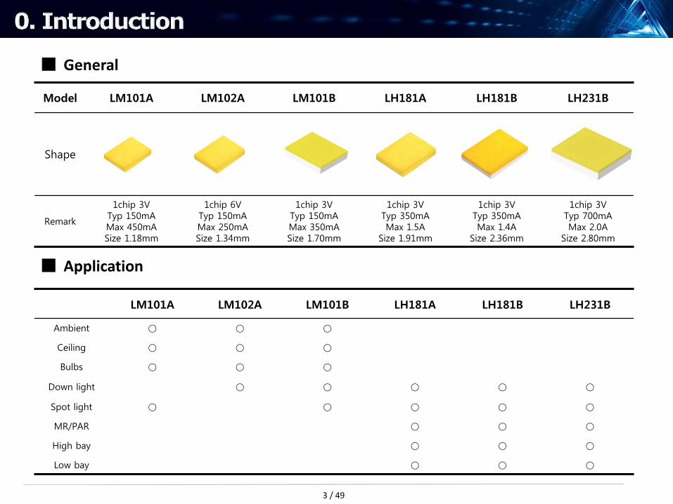
Model LM101A LM102A LM101B LH181A LH181B LH231B
Shape
Remark
1chip 3V Typ 150mA Max 450mA Size 1.18mm
1chip 6V Typ 150mA Max 250mA Size 1.34mm
1chip 3V Typ 150mA Max 350mA Size 1.70mm
1chip 3V Typ 350mA Max 1.5A
Size 1.91mm
1chip 3V Typ 350mA Max 1.4A
Size 2.36mm
1chip 3V Typ 700mA Max 2.0A
Size 2.80mm
■ General
■ Application
LM101A LM102A LM101B LH181A LH181B LH231B
Ambient ○ ○ ○
Ceiling ○ ○ ○
Bulbs ○ ○ ○
Down light ○ ○ ○ ○ ○
Spot light ○ ○ ○ ○ ○
MR/PAR ○ ○ ○
High bay ○ ○ ○
Low bay ○ ○ ○
3 / 49
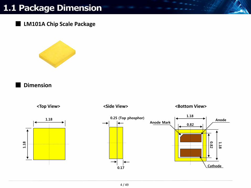
■ LM101A Chip Scale Package
■ Dimension
<Side View> <Top View> <Bottom View>
Anode Mark
Cathode
Anode 1.18
0.82
1.1
8
0.8
2
1.18
1.1
8
0.25 (Top phosphor)
0.17
4 / 49
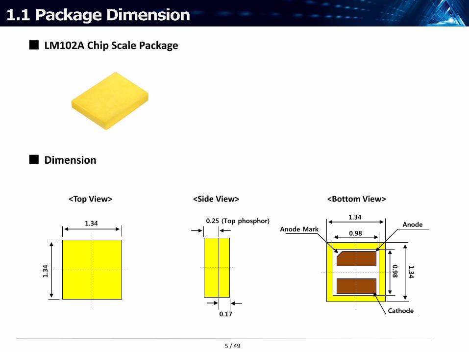
■ LM102A Chip Scale Package
■ Dimension
<Side View> <Top View> <Bottom View>
1.34
1.3
4
0.25 (Top phosphor)
0.17
Anode Mark
Cathode
Anode 1.34
0.98
1.3
4
0.9
8
5 / 49
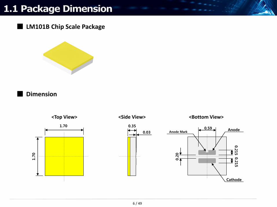
■ LM101B Chip Scale Package
■ Dimension
6 / 49
<Side View> <Top View> <Bottom View>
1.70
1.7
0
0.35
0.03 Anode Mark 0.59
0.2
0
0.2
15
Cathode
Anode
0.2
15
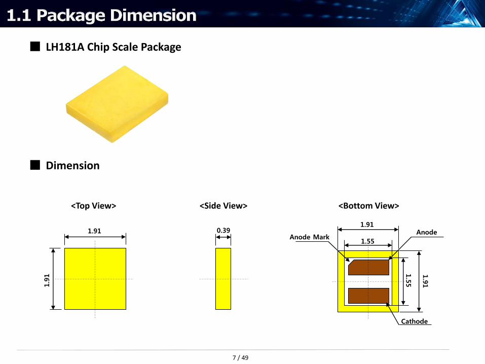
■ LH181A Chip Scale Package
■ Dimension
<Side View> <Top View> <Bottom View>
1.91
1.9
1
Anode Mark
Cathode
Anode 1.91
1.55
1.9
1
1.5
5
0.39
7 / 49
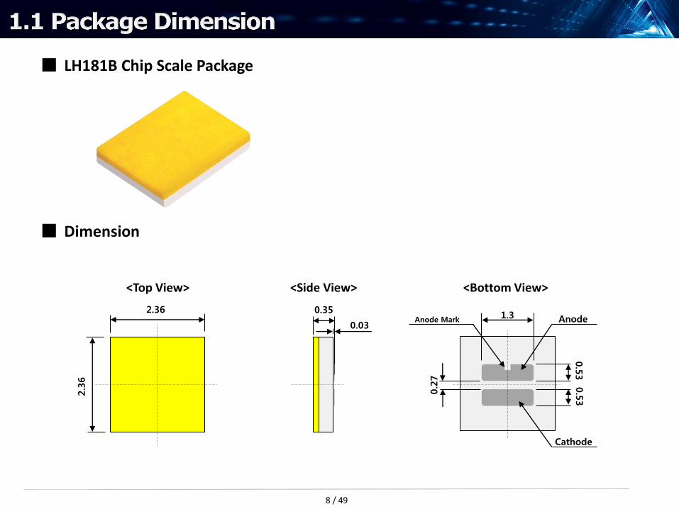
■ LH181B Chip Scale Package
■ Dimension
<Side View> <Top View> <Bottom View>
2.36
2.3
6
0.35
0.03 Anode Mark
1.3
0.2
7
0.5
3
Cathode
Anode
0.5
3
8 / 49
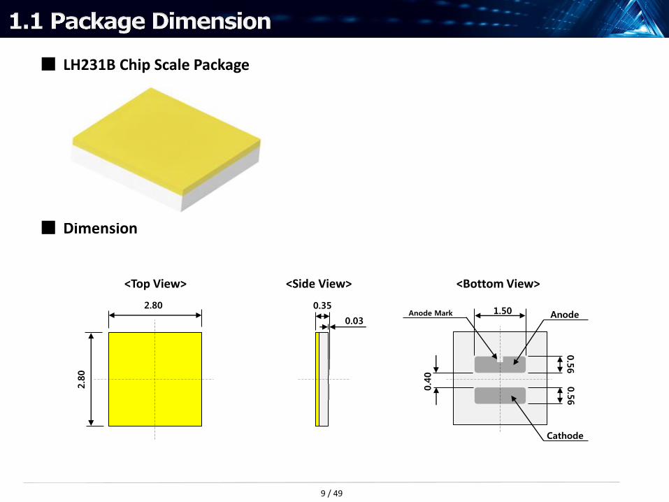
■ LH231B Chip Scale Package
■ Dimension
<Side View> <Top View> <Bottom View>
2.80
2.8
0
0.35
0.03 Anode Mark 1.50
0.4
0
0.5
6
Cathode
Anode
0.5
6
9 / 49
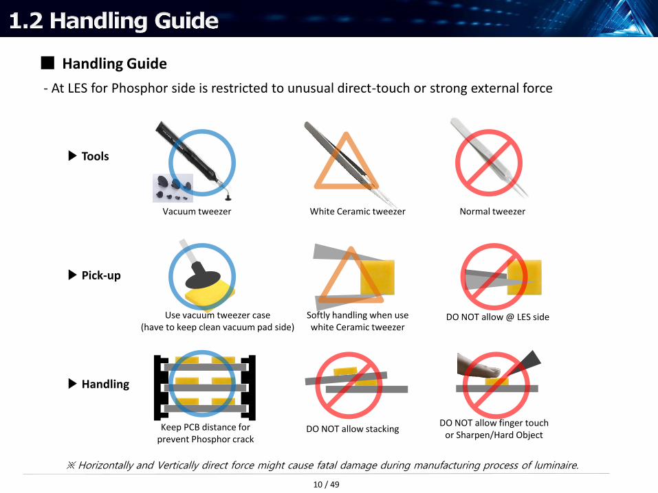
■ Handling Guide
- At LES for Phosphor side is restricted to unusual direct-touch or strong external force
▶ Tools
▶ Pick-up
▶ Handling
White Ceramic tweezer Vacuum tweezer Normal tweezer
Softly handling when use white Ceramic tweezer
Use vacuum tweezer case (have to keep clean vacuum pad side)
DO NOT allow @ LES side
DO NOT allow stacking DO NOT allow finger touch
or Sharpen/Hard Object Keep PCB distance for
prevent Phosphor crack
※ Horizontally and Vertically direct force might cause fatal damage during manufacturing process of luminaire.
10 / 49
Handling PKGs
① Users have not to touch the lighting emitting surface(LES) in any cases.
② When handling with tweezers user have to grip the thermo plastic(white mold).
③ Users have to wear the anti-static gloves or anti-static wrist band.
④ When handling CSP, user have to use the anti-static tweezers. Especially, CSP is strongly recommended to use a vacuum pick-up & place utensils. (Especially, a sharpened-tip of the tweezers would have high possibility of giving a physical defect to CSP)
⑤ When switching on CSP with an electrical power supplier, an unexpected or abrupt current should bring about EOS failure in CSP. This may also bring about the failure in use or the decrease of life time of products. Please discharge the stored voltage
of the power supplier.
Environment of Working place
The working area for assembly luminaire is recommended to be maintained clean for preventing any contamination and keeping workers’ safety. If all working area cannot be maintained clean, at least the space for assembly have to be kept clean and lower humidity in air.
At LES (Lighting Emitting Surface), for CSP phosphor film is restricted to unusual direct-touch or strong external force. This may lead to the deformation or film damage.
■ Handling Guide (Document)
The sharp tip may physically damage the resin of Phosphor Resin or wall.
Prevent ESD
It might be required to use MLCCs, TVS or Zener diodes in order to prevent ESD failures in LED module or luminaire.
Those protection components should be considered and selected depending on the forward voltage of LED module, environment or
additional requirements. (ex. Able to use 10uF 50V MLCC for 24V LED module. Regarding PWM dimming, recommend TVS or other
diodes rather than MLCC due to acoustic noise.)
11 / 49
Chemical compatibility
During manufacturing luminaire, the many chemicals could attack and contaminate PKGs. It is necessary to avoid the contaminants and chemicals in manufacturing process and operation. And we are providing the guideline for chemicals and relevant failure mode. (Refer to chemical guideline).
Contamination and cleaning
In the production process of luminaire, pkgs can be contaminated by an unexpected contaminant. The organic material like as solder flux have to be cleaned out by using the tip of cotton swap soaked isopropyl alcohol(IPA).
When a product are stored in any space the product needs not to be directly contact with ambient air or any packing paper boxes. Some packing materials could lead to give in harmful gases to normal operation of pkgs.
Storage
If the LEDs are to be stored for 3 months or more after being shipped from Samsung Electronics, they should be packed by a sealed container with nitrogen gas. (Shelf life of sealed bags: 12 months, temp. ~40 ℃, ~90 %RH)
CSP have a JEDEC level of 2a. User have to handle CSP by below following guide line, which is based on the JEDEC Moisture Sensitivity Level.
- After sealed bag is to be opened and , CSP, will be surface-mounted on the board, have to be followed the below guide.
a. CSP should be mounted within 672 hours(28 days) at an assembly line with a condition of no more than 30℃/60%RH
b. CSP should be stored at <10 %RH
- After mounting, the residual or extra CSP is recommended to be repack in a gas sealed bag.
- If moisture sensitivity indicator is >60 % at 23±5℃ the recovery work should be carried out at the proper condition. In that case, CSP should be baked at 60±5 ℃
■ Handling Guide (Document)
12 / 49
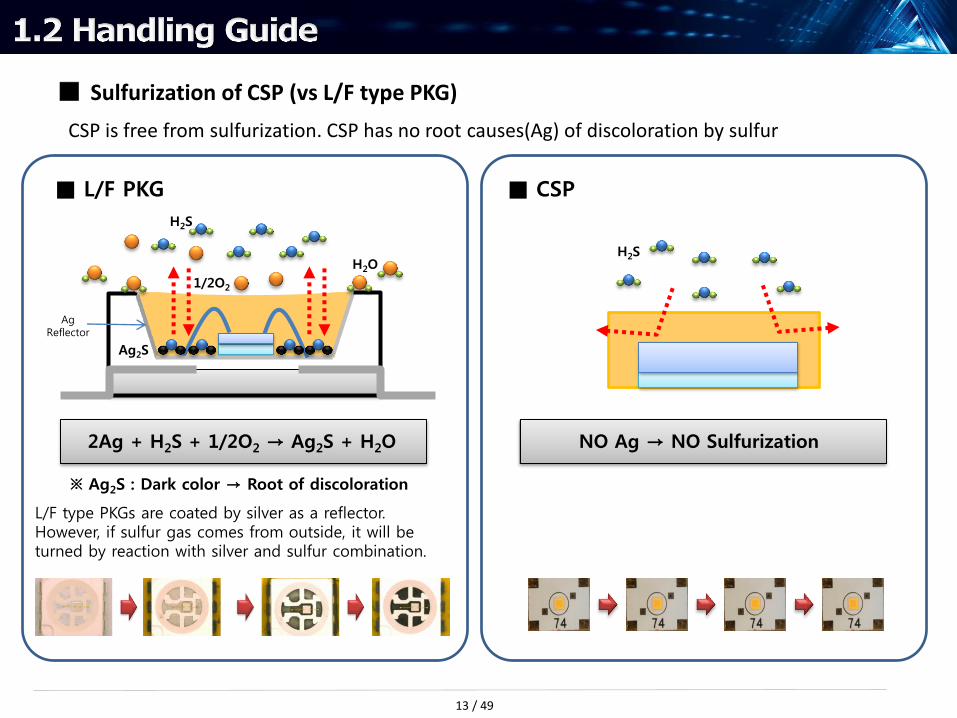
2Ag + H2S + 1/2O2 → Ag2S + H2O
■ L/F PKG
H2S
Ag2S
H2O
1/2O2
H2S
■ CSP
NO Ag → NO Sulfurization
※ Ag2S : Dark color → Root of discoloration
Ag Reflector
L/F type PKGs are coated by silver as a reflector. However, if sulfur gas comes from outside, it will be turned by reaction with silver and sulfur combination.
■ Sulfurization of CSP (vs L/F type PKG)
CSP is free from sulfurization. CSP has no root causes(Ag) of discoloration by sulfur
13 / 49
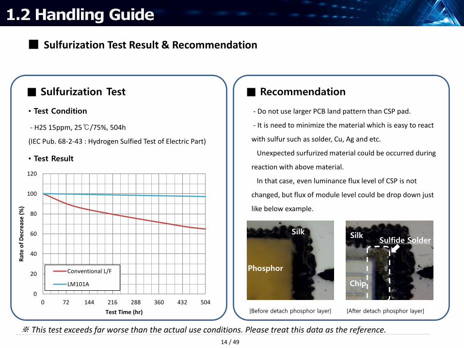
※ This test exceeds far worse than the actual use conditions. Please treat this data as the reference.
0
20
40
60
80
100
120
0 72 144 216 288 360 432 504
Rat
e o
f D
ecr
eas
e (
%)
Test Time (hr)
Conventional L/F
LM101A
■ Sulfurization Test Result & Recommendation
- H2S 15ppm, 25℃/75%, 504h
(IEC Pub. 68-2-43 : Hydrogen Sulfied Test of Electric Part)
- Do not use larger PCB land pattern than CSP pad.
- It is need to minimize the material which is easy to react
with sulfur such as solder, Cu, Ag and etc.
Unexpected surfurized material could be occurred during
reaction with above material.
In that case, even luminance flux level of CSP is not
changed, but flux of module level could be drop down just
like below example.
14 / 49
■ Recommended Land Pattern
LM101A
0.2
4
0.2
5
0.2
5
0.67
Anode Mark
0.82
0.63
0.2
1
0.2
1
0.2
0
0.8
2
Phosphor Wall
0.2
0
0.2
1
0.2
1
0.63
LM102A
PKG PAD
PCB Land
PKG PAD
PCB Land
15 / 49 0.2
0
0.2
4
0.2
4
0.75
LM101B
PKG PAD
PCB Land
Anode Mark 0.59
0.2
0
0.2
15
0.2
15
Anode Mark
0.98
0.67
0.2
5
0.2
5
0.2
4 0
.98
Phosphor Wall
■ Recommended Land Pattern
LH181B
PKG PAD
PCB Land
LH181A
PKG PAD
PCB Land
0.2
7
0.5
3
0.5
3
1.3
0.2
7
0.5
3
0.5
3
1.3
Anode Mark
1.55
1.3
0.5
3
0.5
3
0.2
7 1
.55
Phosphor Wall
Anode Mark 1.3
0.2
7
0.5
3
0.5
3
16 / 49
LH231B
PKG PAD
PCB Land
0.4
0
0.5
6
0.5
6
1.50
Anode Mark 1.50
0.4
0
0.5
6
0.5
6
Process control item (Process setting condition)
Unit Specification Spec. range
LSL Target USL
Solder stir Hours sec 60 - 60 -
Speed rpm 1000 - 1000 -
Solder standing time @ room temperature
Hr 2 2 - 12
Solder Lifetime
After opening Hr within 24 hours Use within 24 hours
Printer status - Volume 70 - 150
SPI spec.
Squeegee Presure ㎏f/㎠ 3 3 4 5
Speed mm/sec 40 30 60 90
Snap-Off Distance Mm 3 - 3 -
Speed mm/sec 1 0.8 1 1.5
Print temperature ℃ 24 20 24 28
Mask Auto-cleaning time/Board 3 - 3 -
Mask Manual cleaning time/Board 15 - 15 -
MASK Lifetime
# of time # time 30,000 - 30,000
tension mm 0.5 0.4 - 0.7
■ Screen Printing
※ Reference Equipment : ESE US-8500X
- Solder Printing : check accurate position, shape, amount of solder paste. - Solder Paste Storage: Should be stored in refrigerator. We can re-use if solder paste store within 24 hour after using at room temperature. In accordance with the relevant regulations it should be used as the correct process. - Squeegees : Should be keep clean after using the squeegee for maintain flatness of squeegee. After usage of over 20,000 times, it should be replaced by new one.
※ Please refer just as a reference
17 / 49
■ Solder Paste Recommendation
- Solder : M705-GRN360-K2 (IV-Type) - Low voiding paste - Paste type recommendations : Pb free, No clean, No water soluble
Max. Temp. gradient in Cooling : -5℃/sec Conveyor Belt Speed : 0.75 m/min
Melting : 220℃~ (60~70sec)
20 / 49
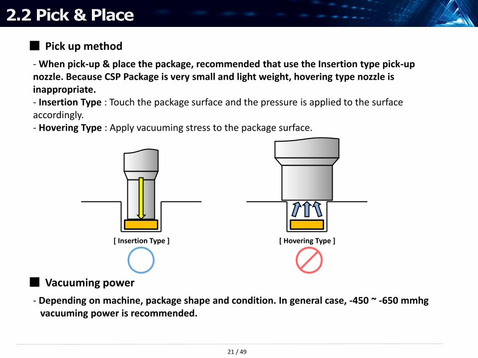
■ Pick up method
- When pick-up & place the package, recommended that use the Insertion type pick-up nozzle. Because CSP Package is very small and light weight, hovering type nozzle is inappropriate. - Insertion Type : Touch the package surface and the pressure is applied to the surface accordingly. - Hovering Type : Apply vacuuming stress to the package surface.
[ Insertion Type ] [ Hovering Type ]
■ Vacuuming power
- Depending on machine, package shape and condition. In general case, -450 ~ -650 mmhg vacuuming power is recommended.
21 / 49
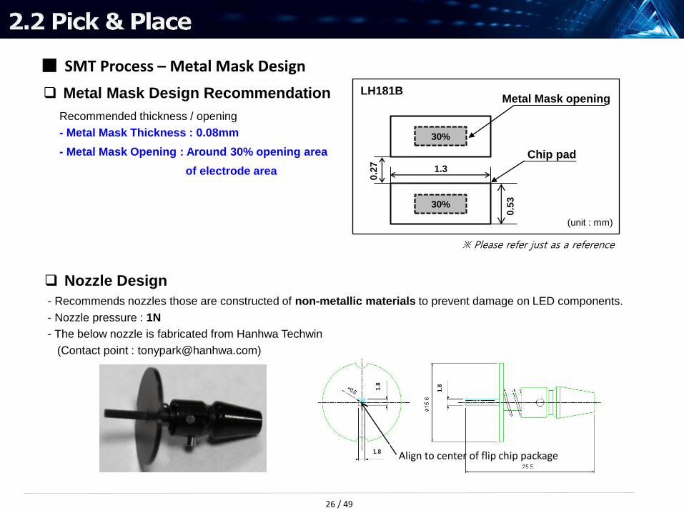
Metal Mask Design Recommendation
Recommended thickness / opening
- Metal Mask Thickness : 0.08 ~ 0.1mm
- Metal Mask Opening : Around 60~70% opening area
of electrode area
Nozzle Design
- Recommends nozzles those are constructed of non-metallic materials to prevent damage on LED components.
- Nozzle pressure : 1N
- The below nozzle is fabricated from Hanhwa Techwin
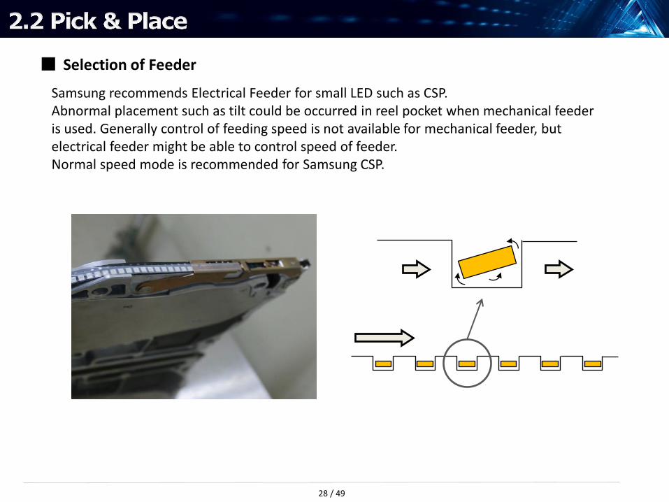
Samsung recommends Electrical Feeder for small LED such as CSP. Abnormal placement such as tilt could be occurred in reel pocket when mechanical feeder is used. Generally control of feeding speed is not available for mechanical feeder, but electrical feeder might be able to control speed of feeder. Normal speed mode is recommended for Samsung CSP.
28 / 49
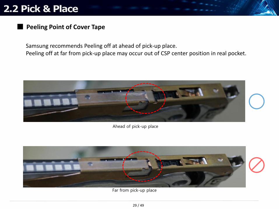
■ Peeling Point of Cover Tape
Samsung recommends Peeling off at ahead of pick-up place. Peeling off at far from pick-up place may occur out of CSP center position in real pocket.
Ahead of pick-up place
Far from pick-up place
29 / 49
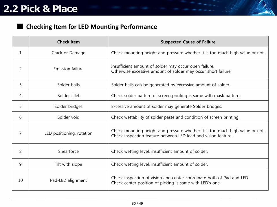
Check item Suspected Cause of Failure
1 Crack or Damage Check mounting height and pressure whether it is too much high value or not.
2 Emission failure Insufficient amount of solder may occur open failure. Otherwise excessive amount of solder may occur short failure.
3 Solder balls Solder balls can be generated by excessive amount of solder.
4 Solder fillet Check solder pattern of screen printing is same with mask pattern.
5 Solder bridges Excessive amount of solder may generate Solder bridges.
6 Solder void Check wettability of solder paste and condition of screen printing.
7 LED positioning, rotation Check mounting height and pressure whether it is too much high value or not. Check inspection feature between LED lead and vision feature.
8 Shearforce Check wetting level, insufficient amount of solder.
9 Tilt with slope Check wetting level, insufficient amount of solder.
10 Pad-LED alignment Check inspection of vision and center coordinate both of Pad and LED. Check center position of picking is same with LED’s one.
■ Checking Item for LED Mounting Performance
30 / 49
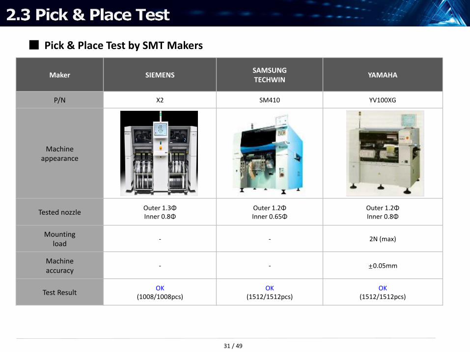
■ Pick & Place Test by SMT Makers
Maker SIEMENS SAMSUNG TECHWIN
YAMAHA
P/N X2 SM410 YV100XG
Machine appearance
Tested nozzle Outer 1.3Φ Inner 0.8Φ
Outer 1.2Φ Inner 0.65Φ
Outer 1.2Φ Inner 0.8Φ
Mounting load
- - 2N (max)
Machine accuracy
- - ±0.05mm
Test Result OK
(1008/1008pcs) OK
(1512/1512pcs) OK
(1512/1512pcs)
31 / 49
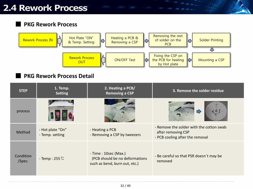
Rework Process IN Hot Plate “ON” & Temp. Setting
Heating a PCB & Removing a CSP
Removing the rest of solder on the
PCB Solder Printing
Mounting a CSP Fixing the CSP on
the PCB for heating by Hot plate
ON/OFF Test Rework Process
OUT
STEP 1. Temp. Setting
2. Heating a PCB/ Removing a CSP
3. Remove the solder residue
process
Method - Hot plate “On” - Temp. setting
- Heating a PCB - Removing a CSP by tweezers
- Remove the solder with the cotton swab after removing CSP - PCB cooling after the removal
Condition /Spec.
- Temp : 255℃ - Time : 10sec (Max.) (PCB should be no deformations such as bend, burn out, etc.)
- Be careful so that PSR doesn`t may be removed
■ PKG Rework Process
■ PKG Rework Process Detail
32 / 49
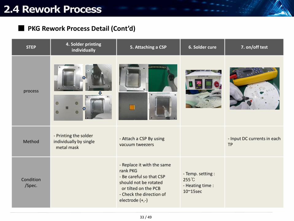
STEP 4. Solder printing
individually 5. Attaching a CSP 6. Solder cure 7. on/off test
process
Method - Printing the solder individually by single metal mask
- Attach a CSP By using vacuum tweezers
- Input DC currents in each TP
Condition /Spec.
- Replace it with the same rank PKG - Be careful so that CSP should not be rotated or tilted on the PCB - Check the direction of electrode (+,-)
- Temp. setting : 255℃ - Heating time : 10~15sec
■ PKG Rework Process Detail (Cont’d)
33 / 49
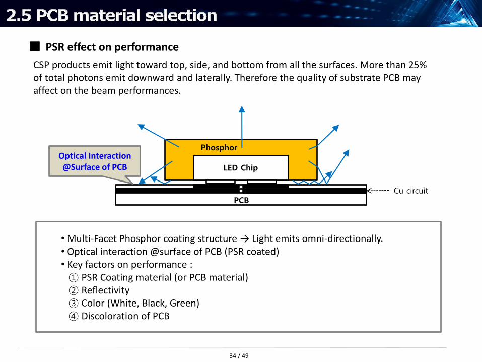
■ PSR effect on performance
• Multi-Facet Phosphor coating structure → Light emits omni-directionally. • Optical interaction @surface of PCB (PSR coated) • Key factors on performance : ① PSR Coating material (or PCB material) ② Reflectivity ③ Color (White, Black, Green) ④ Discoloration of PCB
PCB
LED Chip
Phosphor
Cu circuit
Optical Interaction @Surface of PCB
CSP products emit light toward top, side, and bottom from all the surfaces. More than 25% of total photons emit downward and laterally. Therefore the quality of substrate PCB may affect on the beam performances.
34 / 49
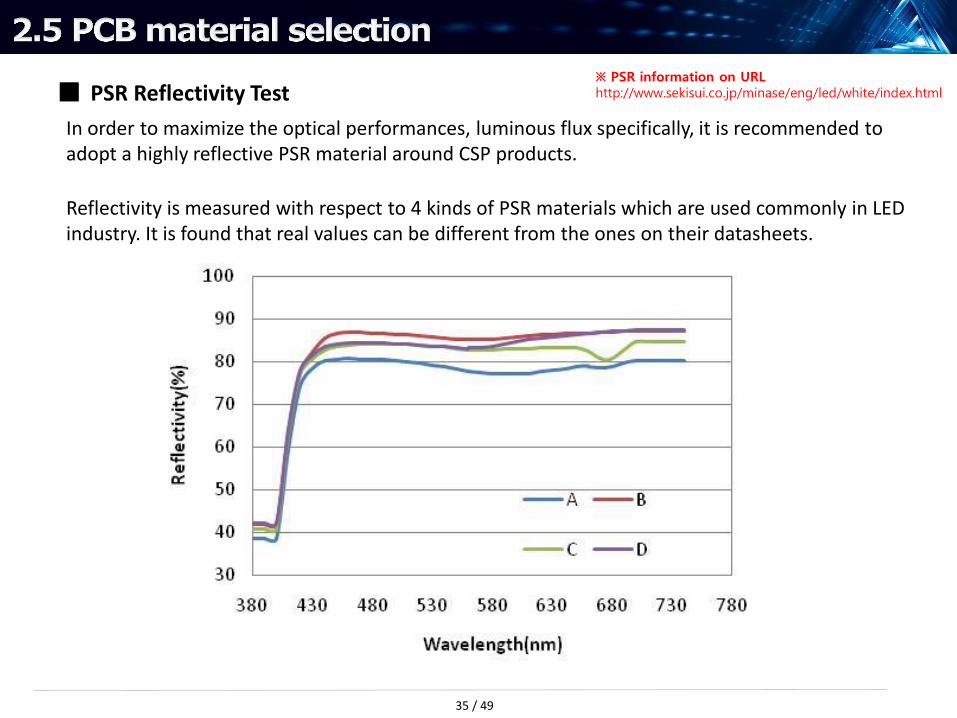
■ PSR Reflectivity Test
In order to maximize the optical performances, luminous flux specifically, it is recommended to adopt a highly reflective PSR material around CSP products.
Reflectivity is measured with respect to 4 kinds of PSR materials which are used commonly in LED industry. It is found that real values can be different from the ones on their datasheets.
※ PSR information on URL http://www.sekisui.co.jp/minase/eng/led/white/index.html
35 / 49
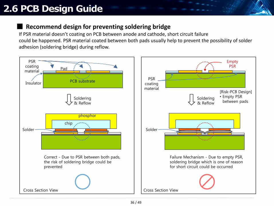
■ Recommend design for preventing soldering bridge If PSR material doesn’t coating on PCB between anode and cathode, short circuit failure could be happened. PSR material coated between both pads usually help to prevent the possibility of solder adhesion (soldering bridge) during reflow.
PCB substrate
Pad
PSR coating material
PSR coating material
Empty PSR
Failure Mechanism - Due to empty PSR, soldering bridge which is one of reason for short circuit could be occurred
Solder
Correct - Due to PSR between both pads, the risk of soldering bridge could be prevented
Solder
chip
phosphor
Soldering & Reflow
Soldering & Reflow
Cross Section View Cross Section View
Insulator
[Risk-PCB Design] • Empty PSR between pads
36 / 49
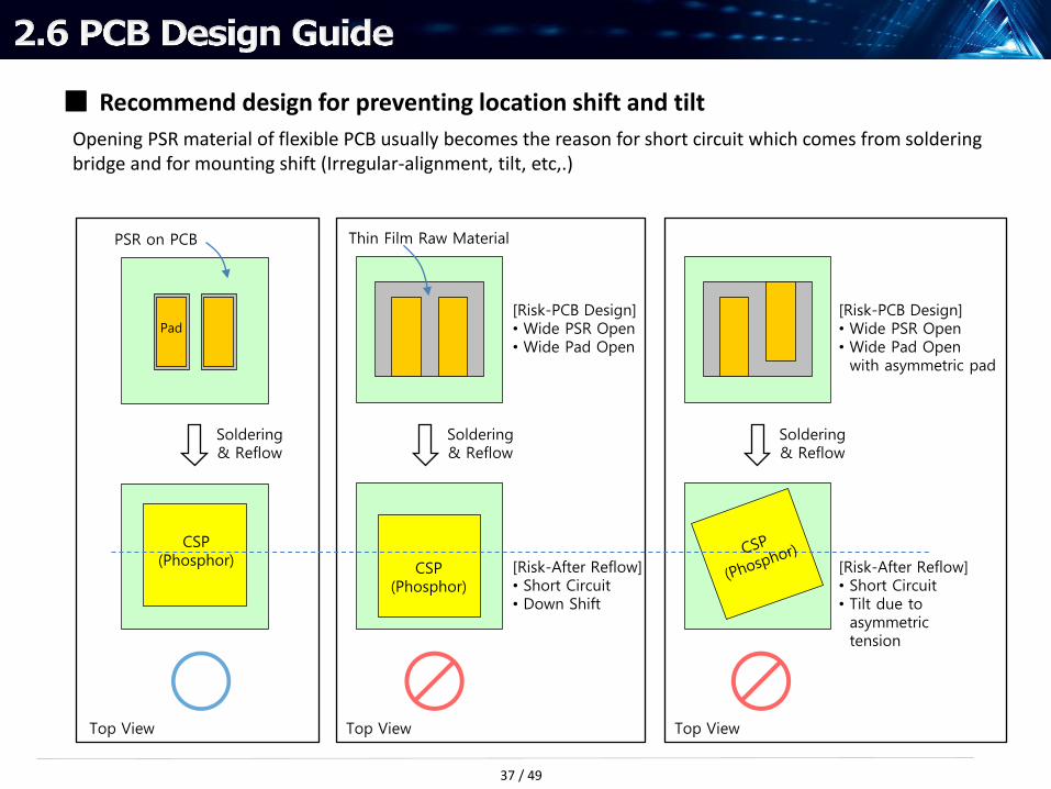
Opening PSR material of flexible PCB usually becomes the reason for short circuit which comes from soldering bridge and for mounting shift (Irregular-alignment, tilt, etc,.)
Soldering & Reflow
CSP (Phosphor)
PSR on PCB
Pad
Top View Top View Top View
Soldering & Reflow
Soldering & Reflow
Thin Film Raw Material
[Risk-After Reflow] • Short Circuit • Down Shift
[Risk-After Reflow] • Short Circuit • Tilt due to asymmetric tension
■ Recommend design for preventing location shift and tilt
[Risk-PCB Design] • Wide PSR Open • Wide Pad Open
[Risk-PCB Design] • Wide PSR Open • Wide Pad Open with asymmetric pad
CSP (Phosphor)
37 / 49
Normally to reduce thermal resistance against insulator within PCB, copper pad were designed to have more wide size for fast spreading heat dissipation. But without PSR coating material, solder could effect electrical damage to LED through the edge side of chip. This could cause result to short circuit failure especially when ceramic PCB design.
■ Recommend design for preventing electrical damage from outside
PCB substrate
Pad
PSR coating material
Correct - Due to well matched pad size between CSP and PCB, there’s no any leakage path
Solder
chip
phosphor
Soldering & Reflow
Cross Section View Cross Section View
Insulator
Wide Pad
Failure Mechanism - Due to wide pad size of PCB, wide spreading solder could effect electrical damage through the edge side of chip (GaN)
Soldering & Reflow
Pad with guided size Pad with wider size than recommendation
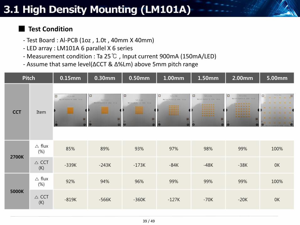
- Test Board : Al-PCB (1oz , 1.0t , 40mm X 40mm) - LED array : LM101A 6 parallel X 6 series - Measurement condition : Ta 25℃ , Input current 900mA (150mA/LED) - Assume that same level(ΔCCT & Δ%Lm) above 5mm pitch range
39 / 49
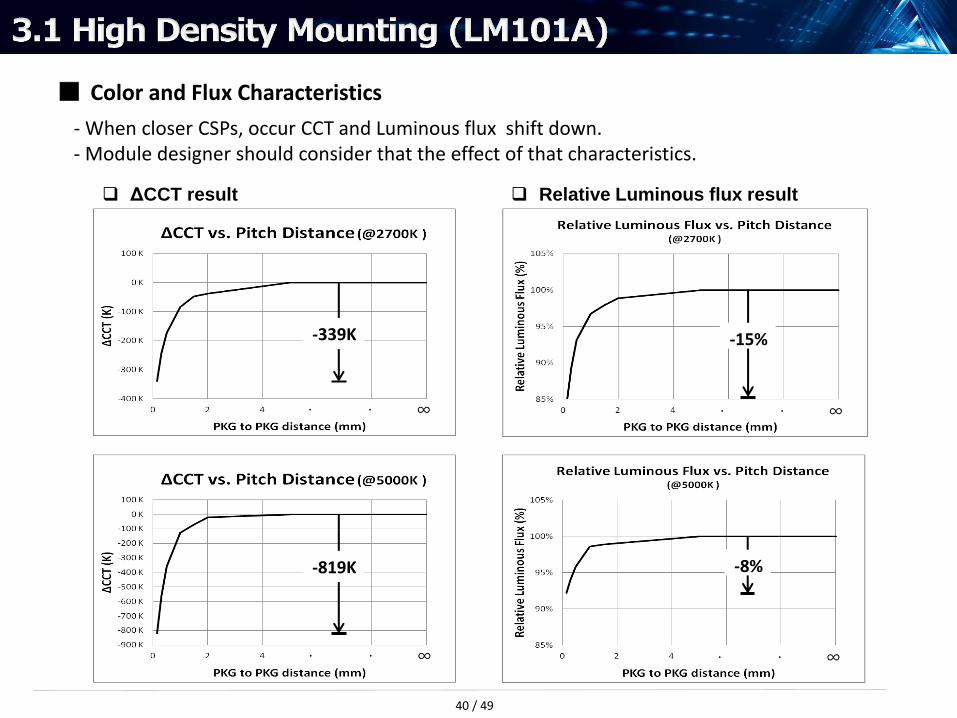
■ Color and Flux Characteristics
· · ∞
-339K
· · ∞
-819K
· · ∞
-15%
· · ∞
-8%
- When closer CSPs, occur CCT and Luminous flux shift down. - Module designer should consider that the effect of that characteristics.
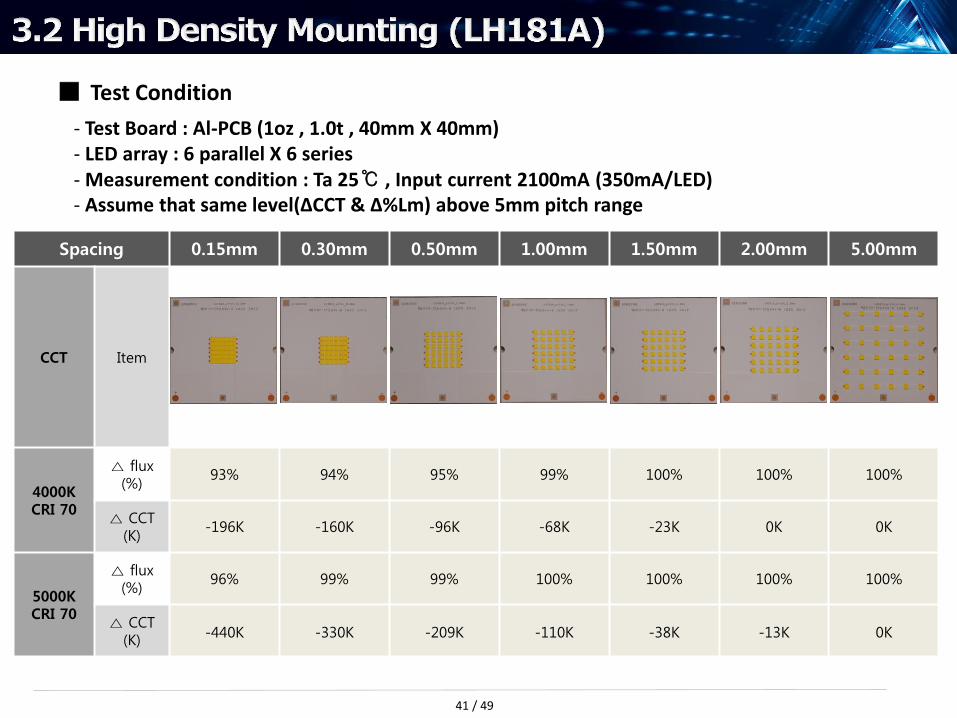
- Test Board : Al-PCB (1oz , 1.0t , 40mm X 40mm) - LED array : 6 parallel X 6 series - Measurement condition : Ta 25℃ , Input current 2100mA (350mA/LED) - Assume that same level(ΔCCT & Δ%Lm) above 5mm pitch range
41 / 49
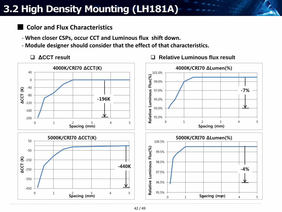
■ Color and Flux Characteristics
- When closer CSPs, occur CCT and Luminous flux shift down. - Module designer should consider that the effect of that characteristics.
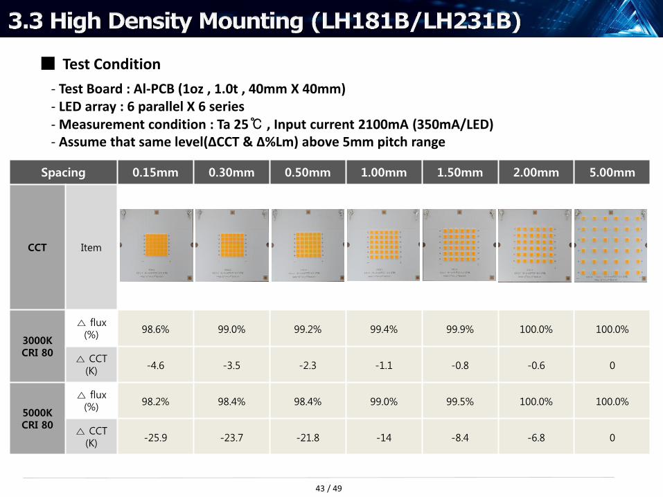
- Test Board : Al-PCB (1oz , 1.0t , 40mm X 40mm) - LED array : 6 parallel X 6 series - Measurement condition : Ta 25℃ , Input current 2100mA (350mA/LED) - Assume that same level(ΔCCT & Δ%Lm) above 5mm pitch range
43 / 49
95.0%
96.0%
97.0%
98.0%
99.0%
100.0%
0 1 2 3 4 5Rela
tive L
um
inous
Flu
x(%
)
Spacing (mm)
3000K/CRI80 ΔLumen(%)
95.0%
96.0%
97.0%
98.0%
99.0%
100.0%
0 1 2 3 4 5Rela
tive L
um
inous
Flu
x(%
)
Spacing (mm)
5000K/CRI80 ΔLumen(%)
-50
-40
-30
-20
-10
0
0 1 2 3 4 5
ΔCCT (
K)
Spacing (mm)
3000K/CRI80 ΔCCT(K)
-50
-40
-30
-20
-10
0
0 1 2 3 4 5
ΔCCT (
K)
Spacing (mm)
5000K/CRI80 ΔCCT(K)
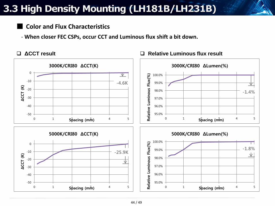
■ Color and Flux Characteristics
- When closer FEC CSPs, occur CCT and Luminous flux shift a bit down.
ΔCCT result Relative Luminous flux result
-4.6K
-25.9K
-1.4%
-1.8%
44 / 49
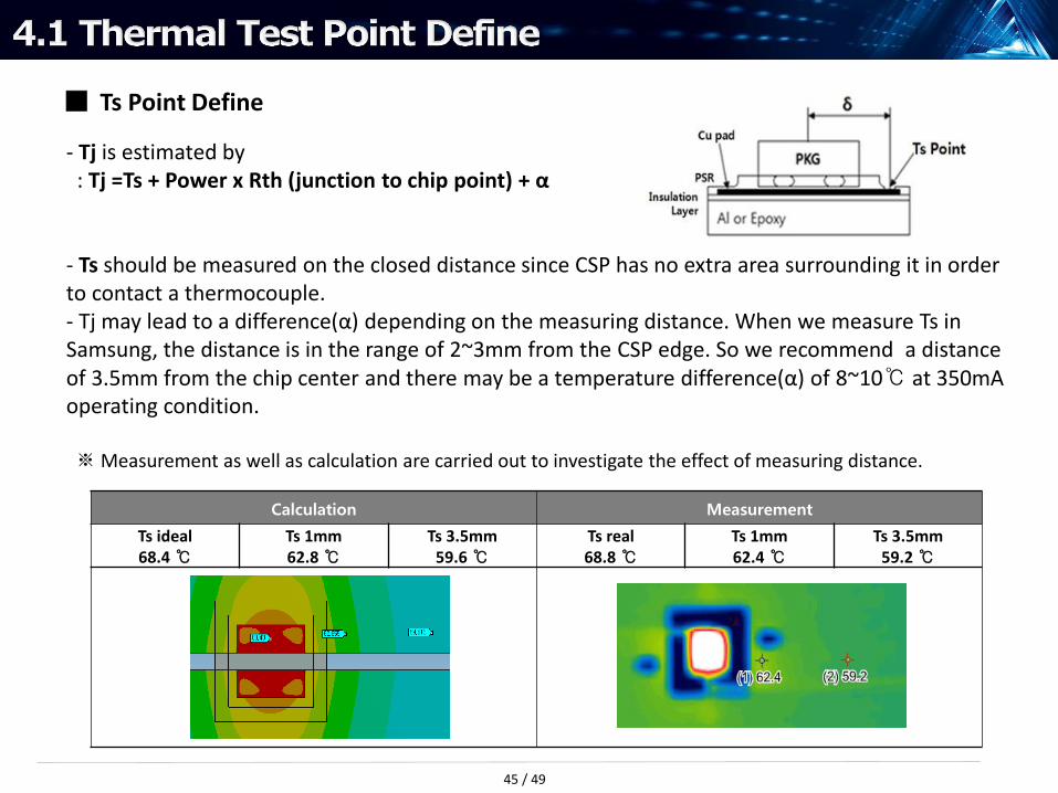
■ Ts Point Define
- Tj is estimated by : Tj =Ts + Power x Rth (junction to chip point) + α - Ts should be measured on the closed distance since CSP has no extra area surrounding it in order to contact a thermocouple. - Tj may lead to a difference(α) depending on the measuring distance. When we measure Ts in Samsung, the distance is in the range of 2~3mm from the CSP edge. So we recommend a distance of 3.5mm from the chip center and there may be a temperature difference(α) of 8~10℃ at 350mA operating condition. ※ Measurement as well as calculation are carried out to investigate the effect of measuring distance.
Calculation Measurement
Ts ideal 68.4 ℃
Ts 1mm 62.8 ℃
Ts 3.5mm 59.6 ℃
Ts real 68.8 ℃
Ts 1mm 62.4 ℃
Ts 3.5mm 59.2 ℃
45 / 49
■ Measurement of a thermal resistance, Rth of LED with T3Ster* tool
* T3Ster : Thermal Transient Tester, developed by Mentor Graphics ** The Structure Function is related with vertical position and Rth of the testing object, supplied by T3Ster.
MCPCB
① The test sample should be smaller than T3STER heat sink but bigger than CSP. - A star board of 20㎜ size is used normally. ② For thermal contact, a thermal grease or a pad should be placed between heat sink and CSP. - Input electric power should not exceed the cooling capacity of T3Ster. ③ From the generated structure function**, Rth values can be derived.
① Sample Preparation
20mm
CSP
[CSP on Star Board]
② Testing CSP using T3STER ③ Evaluating Rth
PC
0 5 10 15 20 25
1e-4
0.01
1
100
10000
Rth [K/W]
K [W
쾠 / K
?
T3Ster Master: differential structure function(s)
20131009 5630G2 STAR MPCB 65mA no3 - Ch. 0
20131005_FCOM_SQRPAD_STARMPCB_65mA_no2 - Ch. 0
20131009 5630G2 STAR MPCB 65mA no1 - Ch. 0
20131005_FCOM_SQRPAD_STARMPCB_65mA_no3 - Ch. 0
[Structure Function]
Rth (℃/W)
K (W
2s/℃
2)
[Schematic work flow to evaluate a thermal resistance of LED]
46 / 49
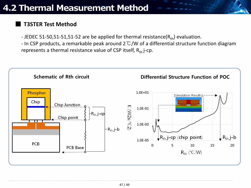
■ T3STER Test Method
- JEDEC 51-50,51-51,51-52 are be applied for thermal resistance(Rth) evaluation. - In CSP products, a remarkable peak around 2℃/W of a differential structure function diagram represents a thermal resistance value of CSP itself, Rth j-cp.
Differential Structure Function of POC Schematic of Rth circuit
47 / 49
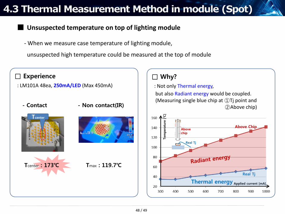
■ Unsuspected temperature on top of lighting module
- When we measure case temperature of lighting module,
unsuspected high temperature could be measured at the top of module
□ Why?
: Not only Thermal energy,
but also Radiant energy would be coupled. (Measuring single blue chip at ①Tj point and ②Above chip)
□ Experience
: LM101A 48ea, 250mA/LED (Max 450mA)
- Contact - Non contact(IR)
Tcenter : 173℃ Tmax : 119.7℃
Tcenter
Above Chip
Real Tj
Applied current [mA]
Tem
pera
ture
[℃
]
Thermal energy
Real Tj
Above chip
48 / 49
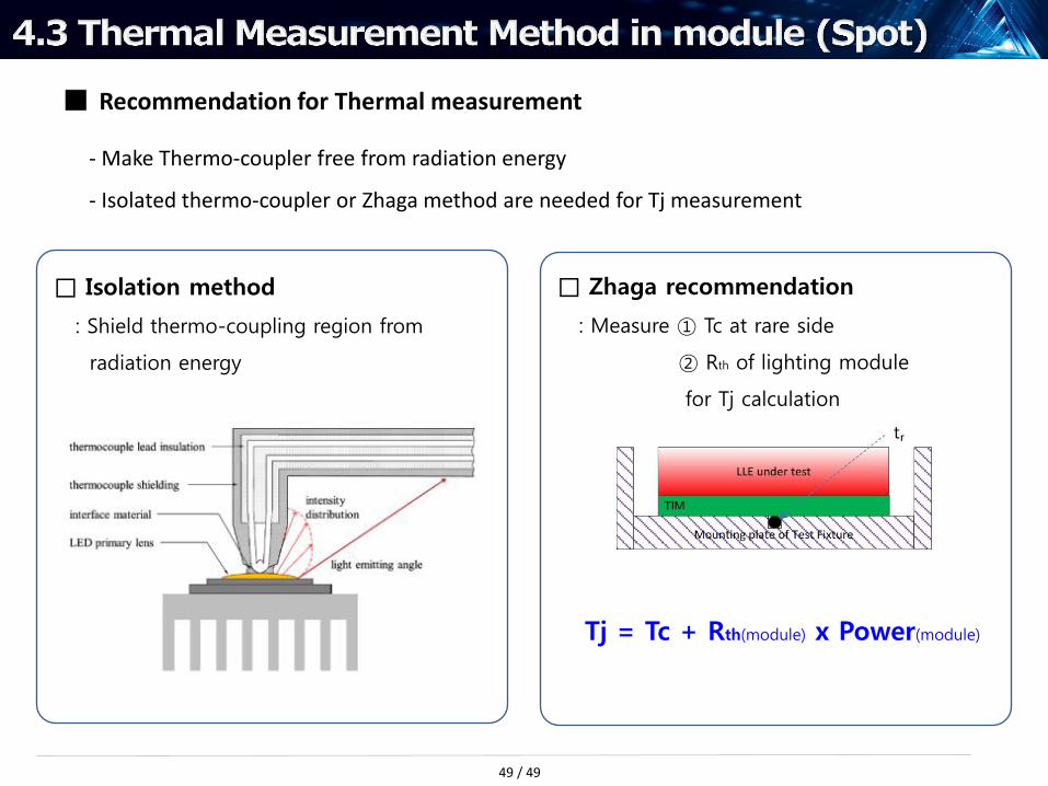
■ Recommendation for Thermal measurement
- Make Thermo-coupler free from radiation energy
- Isolated thermo-coupler or Zhaga method are needed for Tj measurement