Page 1
1300 Henley Court
Pullman, WA 99163
509.334.6306
www.digilentinc.com
ChipKIT Pro MX7 Board Reference Manual
Revised October 15, 2013 This manual applies to the ChipKIT Pro MX7 rev. B and C
DOC#: 502-296 Copyright Digilent, Inc. All rights reserved.
Other product and company names mentioned may be trademarks of their respective owners. Page 1 of 38
Table of Contents
Table of Contents .................................................................................................................. 1
Overview ............................................................................................................................... 3
Functional Description ........................................................................................................... 4
1 Programming Tools ........................................................................................................ 4
1.1 Using the ChipKIT Pro MX7 with Microchip Development Tools..................................... 4
1.2 Using the ChipKIT Pro MX7 with the MPIDE .................................................................... 6
1.3 Additional Reference Documentation ............................................................................. 6
2 Board Power Supply ....................................................................................................... 7
2.1 RESET ................................................................................................................................ 9
3 Pmod™ Connectors ........................................................................................................ 9
4 Digital Inputs and Outputs ........................................................................................... 10
4.1 Push Buttons and LEDs ................................................................................................... 11
4.2 5V Signal Compatibility .................................................................................................. 12
5 CPU Clock Source ......................................................................................................... 12
6 Ethernet Interface ........................................................................................................ 13
7 USB Interface ............................................................................................................... 15
8 CAN Interface ............................................................................................................... 16
Page 2
ChipKIT Pro MX7 Board Reference Manual
Copyright Digilent, Inc. All rights reserved. Other product and company names mentioned may be trademarks of their respective owners. Page 2 of 38
9 UART Interface ............................................................................................................. 17
10 Serial Peripheral Interface (SPI) .................................................................................... 18
11 I2C™ Interface .............................................................................................................. 19
11.1 On-Board I2C Peripheral Device .................................................................................. 21
12 Analog Inputs ............................................................................................................... 21
12.1 A/D Converter Voltage Reference .............................................................................. 22
13 Timers ......................................................................................................................... 22
14 Output Compare .......................................................................................................... 23
15 Input Capture ............................................................................................................... 23
16 External Interrupts ....................................................................................................... 24
17 RTCC ............................................................................................................................ 25
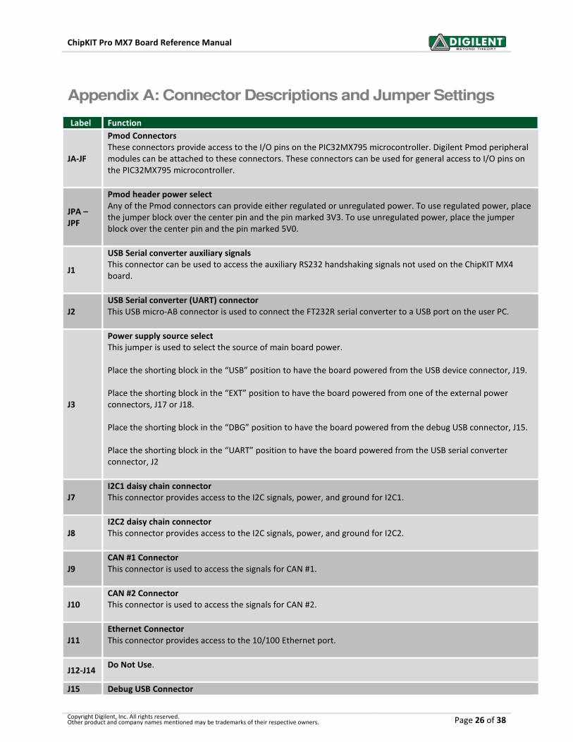
Appendix A: Connector Descriptions and Jumper Settings .................................................... 26
Appendix B: Example of Configuration Values ...................................................................... 29
Appendix C: Connector and Jumper Block Pinout Tables ...................................................... 30
Arranged by Microcontroller Pin Number ................................................................................ 30
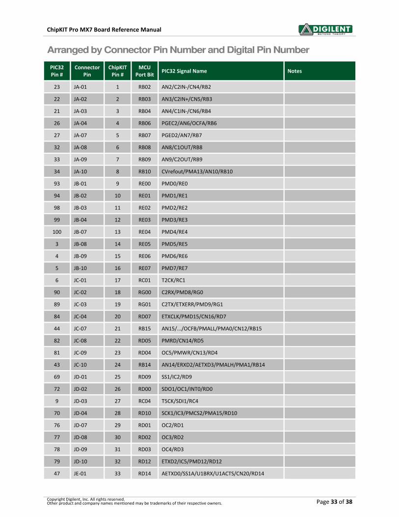
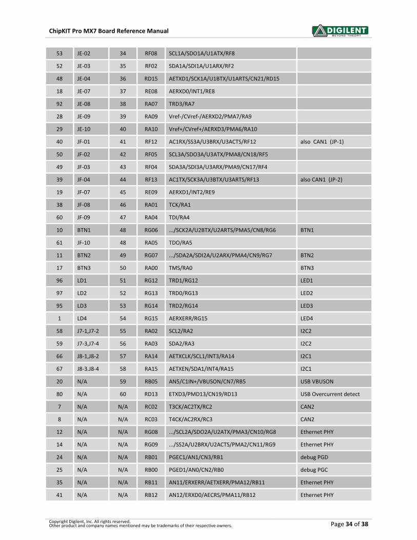
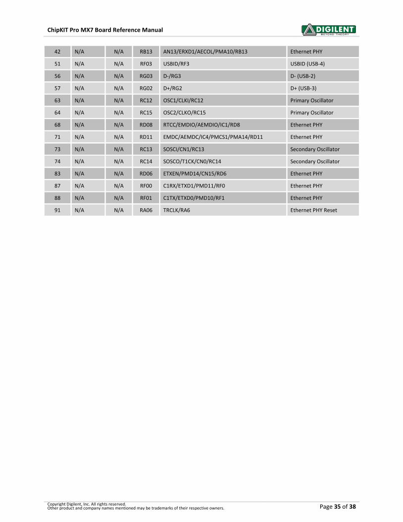
Arranged by Connector Pin Number and Digital Pin Number .................................................. 33
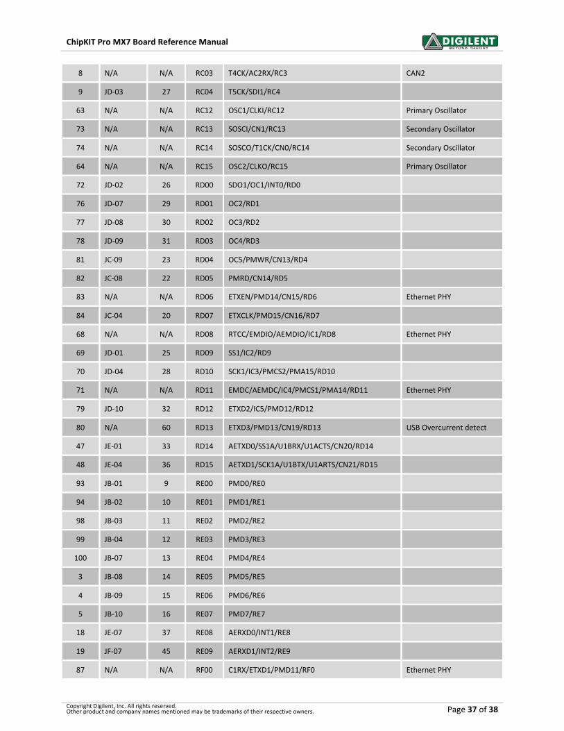
Arranged by Connector Pin Number and Digital Pin Number .................................................. 36
Page 3
ChipKIT Pro MX7 Board Reference Manual
Copyright Digilent, Inc. All rights reserved. Other product and company names mentioned may be trademarks of their respective owners. Page 3 of 38
Overview
ChipKIT Pro MX7is the new name for Cerebot MX7. This board retains all functionality of the Cerebot MX7.
The ChipKIT Pro MX7 is a microcontroller development board based on the Microchip PIC32MX795F512L, a
member of the 32-bit PIC32 microcontroller family. It is compatible with Digilent’s line of Pmod™ peripheral
modules, and is suitable for use with the Microchip MPLAB® IDE tools. The ChipKIT Pro MX7 is also compatible for
use with the chipKIT™ MPIDE development environment. ChipKIT MPIDE is a PIC32 based system compatible with
many existing Arduino™ code examples, reference materials, and other resources.
The ChipKIT Pro MX7 is designed to be easy to use and suitable for use by anyone from beginners to advanced
users for experimenting with embedded control and network communications application. A built in
programming/debugging circuit compatible with the Microchip MPLAB® IDE is provided, so no additional hardware
is required for use with MPLAB. The kit contains everything needed to start developing embedded applications
using either the MPLAB® IDE or the MPIDE.
The ChipKIT Pro MX7 provides 52 I/O pins that support a number of peripheral functions, such as UART, SPI, I2C™
ports, as well as five pulse width modulated outputs and five external interrupt inputs. Its network and
communications features also include a 10/100 Ethernet interface, Full Speed USB 2.0 OTG interface, and dual CAN
network interfaces. Ten of the I/O pins can be used as analog inputs in addition to their use as digital inputs and
outputs.
The ChipKIT Pro MX7 can be powered in various ways via USB, or using an external AC-DC power adapter.
Features of the ChipKIT Pro MX7 include:
• PIC32MX795F512L microcontroller
• Support for programming and debugging within the
Microchip MPLAB development environment
• Support for programming within the chipKIT MPIDE
development environment
• Six Pmod connectors for Digilent peripheral module
boards
• 10/100 Ethernet
• USB 2.0 compatible Device, Host, and OTG support
• Two CAN network interfaces
• Three push buttons
• Four LEDs
• Multiple power supply options, including USB
powered
• ESD protection and short circuit protection for all
I/O pins.
ChipKIT Pro MX7 Board
Page 4
ChipKIT Pro MX7 Board Reference Manual
Copyright Digilent, Inc. All rights reserved. Other product and company names mentioned may be trademarks of their respective owners. Page 4 of 38
Functional Description
The ChipKIT Pro MX7 is designed for embedded control and network communications applications as well as for
general microprocessor experimentation. Firmware suitable for many applications can be downloaded to the
ChipKIT Pro MX7’s programmable PIC32 microcontroller.
The ChipKIT Pro MX7 has a number of input/output connection options, and is designed to work with the Digilent
line of Pmod peripheral modules that provide various input and output functions. For more information, visit
www.digilentinc.com. In addition to the Pmod connectors, the board provides three push buttons and four LEDs
for user I/O, as well as providing connections for two I2C busses. A serial EEPROM is provided on one of the I
2C
busses.
The ChipKIT Pro MX7 features a flexible power supply system with a number of options for powering the board as
well as powering peripheral devices connected to the board. It can be USB powered via the debug USB port, the
USB UART serial port, or the USB device port. It can also be powered from an external 5V power supply.
1 Programming Tools
The ChipKIT Pro MX7 can be used with either the Microchip MPLAB® development environment or the chipKIT
MPIDE development environment. When used with the MPLAB® IDE, in-system-programming and debugging of
firmware running on the PIC32MX795 microcontroller is supported using an on-board programming/debugging
circuit licensed from Microchip.
The ChipKIT Pro MX7 is immediately useable with either the MPLAB IDE or the MPIDE. No additional hardware is
required to use the board with the Microchip MPLAB tools.
1.1 Using the ChipKIT Pro MX7 with Microchip Development Tools
The Microchip MPLAB® IDE or the MPLAB
® X IDE can be used to program and debug code running on the ChipKIT
Pro MX7 board using the built-in programming/debugging circuit.
Features of the PIC32MX795F512L include:
• 512KB internal program flash memory
• 128KB internal SRAM memory
• USB 2.0 compliant full-speed On-The-Go (OTG)
controller with dedicated DMA channel
• 10/100 Ethernet controller
• Two CAN network controllers
• Up to four serial peripheral interfaces (SPI)
• Up to six UART serial interfaces
• Up to four I2C serial interfaces
• Five 16-bit timer/counters
• Five timer capture inputs
• Five compare/PWM outputs
• Sixteen 10-bit analog inputs
• Two analog comparators
ChipKIT Pro MX7 Circuit Diagram
Page 5
ChipKIT Pro MX7 Board Reference Manual
Copyright Digilent, Inc. All rights reserved. Other product and company names mentioned may be trademarks of their respective owners. Page 5 of 38
The MPLAB development environment can be downloaded from the Microchip web site. This software suite
includes a free evaluation copy of the Microchip C32 compiler for use with the PIC32 microcontroller family. The
licensed debugger is compatible with the MPLAB IDE version 8.63 or later or all versions of MPLAB X.
When creating a new project, use the “Configure.Select Device…” menu to specify the PIC32 device being used.
Ensure that the device is set to PIC32MX795F512L.
In order to use the on-board programming/debugging circuit, it must be selected as the debugger or programmer
within the MPLAB IDE. Use the “Debugger.Select Tool” menu, or the “Programmer.Select Tool” menu, and select
“Licensed Debugger” as the programmer or debugger.
The licensed debugger interface uses USB connector J15, labeled DEBUG. Connector J15 is a USB micro-B
connector located on the left side of the board below the Ethernet RJ45 connector. Use a USB-A to micro-B cable
(provided with the board) to connect to an available USB port on the PC.
When the licensed debugger is selected as the programming or debugging device, the MPLAB IDE will check the
version number of the firmware running on the debugger and offer to update if it is out of date with the version of
MPLAB being used.
The PIC32 in-system programming/debugging interface uses two pins on the microcontroller. These devices
support two alternate pin pairs for this interface: PGC1/PGD1 or PGC2/PGD2. The PGC2/PGD2 pair is used by
default. Due to conflicting uses of the microcontroller pins, the ChipKIT Pro MX7 is designed to use the PGC1/PGD1
pair of pins. Because of this, it is necessary to select the use of PGC1/PGD1 for the debugging interface. This is
done using configuration variables set using the #pragma config statement. The following statement must be
used to configure the microcontroller for use with the on-board licensed debugger circuit:
#pragma config ICESEL = ICS_PGx1
The MPLAB IDE may report an error indicating that the device is not configured for debugging until a program
containing this statement has been programmed into the board.
The MCLR pin on the PIC32 microcontroller is used by the hardware programming/debugging interface to reset the
processor. This same pin is used by the USB serial converter to reset the processor when using the MPIDE. It is
possible that the reset function from the USB serial interface can interfere with correct operation of the Microchip
programming and debugging tools. If this happens, jumper JP11 can be used to disconnect the USB serial converter
reset circuit. Remove the shorting block from JP11 to disable the reset circuit. If the shorting block has been
removed, it is necessary to reinstall it on JP11 in order to use the ChipKIT Pro MX7 board with the MPIDE again.
Using the Microchip development tools to program the ChipKIT Pro MX7 will erase the chipKIT boot loader. To use
the board with the MPIDE again, it is necessary to program the boot loader back onto the board. The programming
file for the boot loader programmed into the board by Digilent at the factory is available for download from the
product page for the ChipKIT Pro MX7 on the Digilent web site. Additionally, the boot loader source code is
available in the chipKIT project repository at www.github.com/chipKIT32/pic32-Arduino-Bootloader.
To reprogram the boot loader using MPLAB, perform the following steps:
• Use the “Configure.Select Device …” menu to select the PIC32MX795F512L
• Use the “Programmer.Select Programmer” menu to select the “Licensed Debugger”.
• Use the “File Import…” dialog box to navigate to and select the boot loader programming downloaded from
the Digilent web site. The file name will be something like: chipKIT_Bootloader_MX7.hex
• Use the “Programmer.Program” command to program all memories on the device.
Page 6
ChipKIT Pro MX7 Board Reference Manual
Copyright Digilent, Inc. All rights reserved. Other product and company names mentioned may be trademarks of their respective owners. Page 6 of 38
1.2 Using the ChipKIT Pro MX7 with the MPIDE
ChipKIT and the MPIDE is a PIC32 based hardware and software system compatible with many existing Arduino™
code examples, reference materials, and other resources. The MPIDE development platform was produced by
modifying the Arduino™ IDE and is fully backward compatible with the Arduino IDE. The ChipKIT Pro MX7 board is
designed to be fully compatible with the MPIDE system, version 20111221 or later.
The MPIDE uses a serial communications port to communicate with a boot loader running in the target board. The
serial port on the MX7 board is implemented using an FTDI FT232R USB serial converter. Before attempting to use
the MPIDE with the MX7, the appropriate USB device driver must be installed.
The USB serial converter on the ChipKIT Pro MX7 uses USB connector J2, labeled UART on the board. This
connector is a USB micro-AB, and is located on the lower left side of the board adjacent to the power switch. Use a
standard USB-A to micro-B cable (provided with the board) to connect the board to an available USB port on the
PC.
In the MPIDE, use the “Tools.Board” command to select the ChipKIT Pro MX7 from the list of available boards. Use
the “Tools.Serial Port” command to choose the appropriate serial port from the list of available serial ports on the
PC.
When the MPIDE needs to communicate with the MX7 board, the PIC32 microcontroller is reset and starts running
the boot loader. The MPIDE then establishes communications with the boot loader and downloads the user’s
program, programming it into the flash memory in the microcontroller
When the MPIDE opens the serial communications connection on the PC, the DTR pin on the FT232R chip is driven
low. This pin is coupled through a capacitor to the MCLR pin on the PIC32 microcontroller. Driving the MCLR line
low resets the microcontroller, restarting execution with the boot loader.
The automatic reset action when the serial communications connection is opened can be disabled. To disable this
operation, remove the shorting block from jumper JP11. The shorting block is reinstalled on JP11 to restore
operation with the MPIDE.
Two red LEDs (LD9 and LD10) will blink when data is being sent or received between the ChipKIT Pro MX7 and the
PC over the serial connection.
The header connector J1 provides access to the other serial handshaking signals provided by the FT232R.
Connector J1 is not loaded at the factory but can be installed by the user to access these signals.
1.3 Additional Reference Documentation
Additional information about the ChipKIT Pro MX7 board and the use and operation of the PIC32MX795F512L
microcontroller can be obtained from the following sources.
The ChipKIT Pro MX7 Schematic, various support libraries, and example reference designs are available on the
board product page on the Digilent web site: www.digilentinc.com
The PIC32MX5XX/6XX/7XX Family Data Sheet and the PIC32MX Family Reference Manual are available from the
Microchip web site: www.microchip.com
Page 7
ChipKIT Pro MX7 Board Reference Manual
Copyright Digilent, Inc. All rights reserved. Other product and company names mentioned may be trademarks of their respective owners. Page 7 of 38
Reference material for the MPIDE system is included in the MPIDE software download and on-line in the chipKIT
wiki. Help with questions and problems using the board with the MPIDE software can also be obtained in the
chipKIT forums:
www.github.com/chipKIT32 (software download)
www.chipKIT.org/wiki
www.chipKIT.org/forum
2 Board Power Supply
Switch SW1 in the lower left corner of the board is the power switch. Place this switch in the ON position to turn
on board power and in the OFF position to turn off board power.
The ChipKIT Pro MX7 may be USB powered via either the USB debug port, the USB UART port, or the USB device
port. Alternatively, the board may be powered via dedicated “external” power supply connectors.
Jumper block J3 selects the power source used to provide power to the board. This jumper block provides the
following four positions:
• USB – power is supplied by USB device connector J19. This is used when the ChipKIT Pro MX7 is being used to
implement a USB bus powered device.
• EXT – Power is supplied by one of the external power connectors.
• DBG – Power is supplied by DEBUG USB connector J15.
• UART – Power is supplied by UART USB connector J2.
Place the shorting block in the appropriate position on J3 for the desired power source for the board.
The ChipKIT Pro MX7 is rated for external power from 3.6 to 5.5 volts DC. Using a voltage outside this range will
damage the board and connected devices. For most purposes when using external power, a regulated 5V supply
should be used. If the board is operated from an external supply with a voltage less than 5V, some features won’t
work correctly.
The USB specification requires that USB devices not draw more than 100mA of current until they have enumerated
on the USB bus and informed the host that they want to consume more current. To meet this specification, the
debugger circuit turns on main board power by driving the PWR_ON signal high after successfully enumerating on
the USB bus. The bus labeled on the schematic as VCC5V0 is powered when this occurs. The VCC5V0 bus powers
the input to the main board voltage regulator, the input voltage to the USB bus voltage load switch used when
using the board as a USB host, the power supply voltage for the CAN transceivers, and the 5V0 side of the power
select jumpers for the Pmod connectors. The voltage on the VCC5V0 bus will be 5V when the board is being
operated from USB power or an external regulated 5V supply. If a different external supply voltage is used, that
voltage will appear on the VCC5V0 bus.
The power supply selected by the shorting block on J3 will appear on the input power supply bus, labeled VIN in
the schematic. This voltage is regulated to 3.3V to power the licensed debugger circuit by IC11, a Microchip
MCP1801 Low Dropout voltage regulator. This regulator is turned on and the debugger circuit is powered
whenever the power switch is in the on position. The VIN power bus also supplies power to IC9, a PFET load switch
used to turn main board power on or off.
When the power switch is turned on, transistor Q7A attempts to drive the ON/OFF pin of IC9 high to enable the
main power supply.
Page 8
ChipKIT Pro MX7 Board Reference Manual
Copyright Digilent, Inc. All rights reserved. Other product and company names mentioned may be trademarks of their respective owners. Page 8 of 38
If the licensed debugger is connected to an active USB port, it initially disables the main power supply by holding
the PWR_ON signal low. This causes Q8B to hold the ON/OFF pin of IC9 low, forcing the main supply off. The
licensed debugger will enumerate with the host computer and once it has successfully enumerated, will turn on
the main board power supply by driving the PWR_ON signal high.
If the licensed debugger is not connected to an active USB port, the signal labeled DBG5V0 will not be powered.
Transistor Q8B will be unable to hold the ON/OFF pin low and the main power supply will be turned on
immediately when the power switch is turned on. When load switch IC9 is turned on, it powers the board
unregulated power bus VCC5V0, which provides the input power to the main regulator.
The main board power supply is a switch mode voltage regulator implemented using a Microchip MCP16301
switch mode step-down regulator, IC10. This regulator provides 3.3V at up to 600 mA with approximately 96%
efficiency. When the main power supply is enabled, it powers the regulated power bus VCC3V3
When powering the board from an external power supply, there are two connectors that can be used: J17 and J18.
The barrel connector, J17, is used to power the board from a “wall wart” style power supply. This type of power
supply is available from many sources. Digilent has a power supply available, the 5V Switching Power Supply, which
can be used with connector J17. Connector J17 is a 2.5mm x 5.5mm coaxial connector wired with the center
terminal as the positive voltage.
Connector J18 is a screw terminal connector for an alternative power supply connection for use with battery packs,
bench supplies, or other power sources where use of a hard wired power supply is desirable.
Connectors J17 and J18 are wired in parallel and connect to the EXT position on the Power Select jumper block J3.
A shorting block should be placed on the “EXT” position of J3 when using this option for board power. Only one of
the external power connectors should be used at a time. If multiple power supplies are connected simultaneously,
damage to the board or the power supplies may occur.
When the ChipKIT Pro MX7 is operating as a USB host, an external power supply connected to either J17 or J18
must be used to power the board. In addition to powering the logic on the ChipKIT Pro MX7 board, this supply
provides the USB bus voltage supplied to any connected USB device and must be a regulated 5V with at least
500mA current capability to meet the USB specifications.
The CAN bus operates at 5V, and therefore the transceivers for the two CAN interfaces require 5V to operate
correctly and within the CAN specification. When using the CAN network interfaces, the board should be operated
from a 5V supply if using an external power supply.
The PIC32 microcontroller and on-board I/O devices operate at a supply voltage of 3.3V provided by the VCC3V3
bus. The main voltage regulator is capable of providing a maximum of 600mA of current. The PIC32 microcontroller
will use approximately 85mA when running at 80MHz. The SMSC LAN8720 Ethernet PHY consumes approximately
45mA when operating at 100Mbps. The Microchip MCP2551 CAN transceivers can draw up to 75mA each when
operating the CAN busses. The other circuitry on the board will draw 10-20 mA. The remaining current is available
to provide power to attached Pmods and I2C devices.
The ChipKIT Pro MX7 can provide power to any peripheral modules attached to the Pmod connectors, JA-JF, and to
I2C devices powered from the I
2C daisy chain connectors, J7 and J8. Each Pmod connector provides power pins
that can be powered from either the switched main power bus, VCC5V0, or regulated voltage, VCC3V3, by setting
the voltage jumper block to the desired position. The I2C connectors only provide the regulated voltage, VCC3V3.
Page 9
ChipKIT Pro MX7 Board Reference Manual
Copyright Digilent, Inc. All rights reserved. Other product and company names mentioned may be trademarks of their respective owners. Page 9 of 38
2.1 RESET
A reset button is at the upper right corner of the board. Pressing this button will reset the PIC32 microcontroller.
3 Pmod™ Connectors
The ChipKIT Pro MX7 has six connectors for connecting Digilent Pmod peripheral modules. The Pmod connectors
labeled JA–JF, are 2x6 pin, right-angle, female pin header connectors. Each connector has an associated power
select jumper block labeled JPA–JPF.
Digilent Pmods are a line of small peripheral modules that provide various kinds of I/O interfaces. The Pmod
product line includes such things as button, switch and LED modules, connector modules, LCD displays, high
current output drivers, various kinds of RF interfaces, and many others.
There are two styles of Pmod connector: six-pin and twelve-pin. Both connectors use standard pin headers with
100mil spaced pins. The six-pin connectors have the pins in a 1x6 configuration, while the twelve-pin connectors
use a 2x6 configuration. All of the Pmod connectors on the ChipKIT Pro MX7 are twelve pin connectors.
Six-pin Pmod connectors provide four I/O signals, ground and a switchable power connection. The twelve-pin
connectors provide eight I/O signals, two power pins, and two ground pins. The twelve-pin connectors have the
signals arranged so that one twelve-pin connector is equivalent to two of the six-pin connectors. Pins 1–4 and 7–10
are the signal pins, pins 5 and 11 are the ground pins, and pins 6 & 12 are the power supply pins.
The pin numbering that Digilent uses on the twelve-pin Pmod connectors is non-standard. The upper row of pins
are numbered 1–6, left to right (when viewed from the top of the board), and the lower row of pins are numbered
7–12, left to right. This is in keeping with the convention that the upper and lower rows of pins can be considered
to be two six-pin connectors stacked. When viewed from the end of the connector, pin 1 is the upper right pin and
pin 7 is immediately below it (closer to the PCB).
Each Pmod connector has an associated power select jumper. These are used to select the power supply voltage
supplied to the power supply pins on the Pmod connector. They are switchable between either the unregulated
power supply, VCC5V0, or the 3.3V main board supply, VCC3V3. Place the shorting block in the 3V3 position for
regulated 3.3V and in the 5V0 position to use the unregulated supply.
Each signal pin on the Pmod connectors is connected to an input/output pin on the PIC32 microcontroller. Each pin
has a 200 ohm series resistor and an ESD protection diode. The series resistor provides short circuit protection to
prevent damaging the I/O block in the microcontroller if the pin is inadvertently shorted to VDD or GND, or two
outputs are shorted together. The ESD protection diode protects the I/O block from damage due to electro-static
discharge.
The 200 ohm resistor in series with each I/O pin limits the amount of current that can be sourced from the
microcontroller pins. There will be a 200mV voltage drop per mA of current sourced by the pin. This will not be a
problem when driving typical, high impedance, logic inputs, but can be problematic when trying to drive low
impedance inputs. In some cases it may be necessary to use external buffers when trying to drive low impedance
inputs.
Although ESD protection is provided between the connector pins and the microcontroller pins, ESD safe handling
procedures should be followed when handling the circuit board. The pins on the microcontroller and other circuits
on the board are exposed and can be damaged through ESD when handling the board.
Page 10
ChipKIT Pro MX7 Board Reference Manual
Copyright Digilent, Inc. All rights reserved. Other product and company names mentioned may be trademarks of their respective owners. Page 10 of 38
Digilent Pmod peripheral modules can either be plugged directly into the connectors on the ChipKIT Pro MX7 or
attached via cables. Digilent has a variety of Pmod interconnect cables available.
See the Pinout Tables in Appendix C for more information about connecting peripheral modules and other devices
to the ChipKIT Pro MX7. These tables describe the mapping between pins on the PIC32MX795 microcontroller and
the pins on the various connectors.
The PIC32 microcontroller can source or sink a maximum of 18mA on all digital I/O pins. However, to keep the
output voltage within the specified input/output voltage range (VOL 0.4V, VOH 2.4V) the pin current must be
restricted to +7/-12mA. The maximum current that can be sourced or sunk across all I/O pins simultaneously is +/-
200mA. The maximum voltage that can be applied to any digital I/O pin is 5.5V. The maximum voltage that can be
applied to any analog input capable pin is 3.6V. For more detailed specifications, refer to the
PIC32MX5XX/6XX/7XX Family Data Sheet.
4 Digital Inputs and Outputs
The ChipKIT Pro MX7 board provides access to 48 of the I/O pins from the PIC32MX795 microcontroller via the
Pmod connectors. Four additional I/O pins can be accessed via the I2C connectors, J7 and J8. Any of the pins on the
Pmod or I2C connectors can be individually accessed for digital input or output. Note that when the I
2C signals on
J7 or J8 are being used for I2C communications, they are not available for general purpose I/O.
On PIC32 microcontrollers, the input/output pins are grouped into I/O Ports and are accessed via peripheral
registers in the microcontroller. There are seven I/O Ports numbered A–G and each of the ports are 16 bits wide.
Depending on the particular PIC32 microcontroller, some of the I/O Ports are not present, and not all 16 bits are
present in all I/O Ports.
Each I/O Port has four associated registers: TRIS, LAT, PORT, and ODC. The registers for I/O Port A are named
TRISA, LATA, PORTA, and ODCA. The registers for the other I/O Ports are named similarly.
The TRIS register is used to set the pin direction. Setting a TRIS bit to 0 makes the pin an output. Setting the TRIS
bit to 1 makes the pin an input.
The LAT register is used to write to the I/O Port. Writing to the LAT register sets any pins configured as outputs.
Reading from the LAT register returns the last value written.
The PORT register is used to read from the I/O Port. Reading from the PORT register returns the current state of all
of the pins in the I/O Port. Writing to the PORT register is equivalent to writing to the LAT register.
PIC32 microcontrollers allow any pin set as an output to be configured as either a normal totem-pole output or as
an open-drain output. The ODC register is used to control the output type. Setting an ODC bit to 0 makes the pin a
normal output and setting it to 1 makes the pin an open drain output.
Refer to the PIC32MX5XX/6XX/7XX Family Data Sheet, and the PIC32 Family Reference Manual, Section 12, I/O
Ports, for more detailed information about the operation of the I/O Ports in the microcontroller.
Pmod connector JF, pins 8, 9, and 10 are connected to the signals TCK/RA1, TDI/RA4, and TDO/RA5 respectively.
These microcontroller pins are shared between general purpose I/O functions and use by the JTAG controller. The
JTAG controller is enabled on reset, so these pins are not available for general purpose I/O until the JTAG
controller is disabled. The following statement can be used to disable the JTAG controller:
DDPCONbits.JTAGEN = 0;
The JTAG controller is disabled by the startup initialization code in the MPIDE runtime. It is not necessary to disable
the JTAG controller when using the board with MPIDE.
Page 11
ChipKIT Pro MX7 Board Reference Manual
Copyright Digilent, Inc. All rights reserved. Other product and company names mentioned may be trademarks of their respective owners. Page 11 of 38
The MPIDE system uses logical pin numbers to identify digital I/O pins on the connectors. These pin numbers start
with pin 0 and are numbered up consecutively.
On the ChipKIT Pro MX7, pin numbers 0-47 are used to access the pins on the Pmod connectors and pin numbers
55-58 are used for the signal pins on the I2C connectors, J7 and J8. The pin numbers are assigned so that connector
JA pin 1 (JA-01) is digital pin 0, JA pin 2 (JA-02) is digital pin 1, and so on.
Pins 0-7 are on connector JA, pins 8-15 on JB, pins 16-23 on JC, pins 24-31 and so on. Refer to the tables in
Appendix B for detailed information about the pin mapping between Pmod connector, logical pin number, and
PIC32 microcontroller pin number and pin function.
When using the ChipKIT Pro MX7 with the MPIDE, the functions pinMode(), digitalRead(), and digitalWrite() are
used for digital pin I/O.
The pinMode() function is used to set the pin direction. Pin direction can be set to: INPUT, OUTPUT, or OPEN.
OPEN is used for open-drain and implies output.
The digitalRead() and digitalWrite() functions are used to read or write the pins. DigitalRead() returns the current
state of the specified pin, and digitalWrite() is used to set the state of an output pin. The pin state can be either
HIGH or LOW.
4.1 Push Buttons and LEDs
The ChipKIT Pro MX7 board provides three push button switches for user input and four LEDs for output. The
buttons, BTN1 and BTN2 are connected to I/O Port G, bits 6 and 7 respectively. BTN3 is connected to I/O Port A, bit
0. To read the buttons, pins 6 and 7 of I/O Port G and pin 0 of I/O Port A must be configured as inputs by setting
the corresponding bits in the TRISG and TRISA registers. The button state is then obtained by reading the PORTG or
PORTA registers. When a button is pressed, the corresponding bit will be high (‘1’). The pins used by the buttons
are dedicated to this use and do not appear on any connector.
Button BTN3 is connected to the signal TMS/RA0 on the PIC32 microcontroller. This microcontroller pin is shared
between general purpose I/O functions and use by the JTAG controller. The JTAG controller is enabled on reset,
and so BTN3 is not useable as a button input until the JTAG controller is disabled. The following statement can be
used to disable the JTAG controller:
DDPCONbits.JTAGEN = 0;
The JTAG controller is disabled by the startup initialization code in the MPIDE runtime. It is not necessary to disable
the JTAG controller when using the board with MPIDE.
The four LEDs are connected to bits 12-15 of I/O Port G. LED 1 is connected to bit 12; LED 2 is connected to bit 13,
and so on. These four pins are dedicated to use with the LEDs and do not appear on any connector pin. To use the
LEDs, configure the desired bits as outputs by clearing the corresponding bits in the TRISG register. The state of an
LED is set by writing values to the LATG register. Setting a bit to 1 will illuminate the LED and setting the bit to 0
will turn it off.
When using the MPIDE and the chipKIT system, the buttons are accessed using digitalRead() and the LEDs using
digitalWrite(). Use the following pins to access them:
• BTN1 – PIN_BTN1, pin 48, RG6
• BTN2 – PIN_BTN2, pin 49, RG7
Page 12
ChipKIT Pro MX7 Board Reference Manual
Copyright Digilent, Inc. All rights reserved. Other product and company names mentioned may be trademarks of their respective owners. Page 12 of 38
• BTN3 – PIN_BTN3, pin 50, RA0
• LD1 – PIN_LED1, pin 51, RG12
• LD2 – PIN_LED2, pin 52, RG13
• LD3 – PIN_LED3, pin 53, RG14
• LD4 – PIN_LED4, pin 54, RG15
4.2 5V Signal Compatibility
The PIC32 microcontroller operates at 3.3V and the I/O pins provide 3.3V logic levels; however, it is possible in
some circumstances to use the ChipKIT Pro MX7 to operate with 5V logic devices.
There are two issues to consider when dealing with 5V compatibility for 3.3V logic. The first is protection of 3.3V
inputs from damage caused by 5V signals. The second is whether the 3.3V output is high enough to be recognized
as a logic high value by a 5V input.
The digital only I/O pins on the PIC32 microcontroller are 5V tolerant. It is safe to apply 5V logic signals directly to
these pins without risk of damage to the microcontroller.
The analog capable I/O pins on the PIC32 are not 5V tolerant. The absolute maximum voltage rating for the analog
pins is 3.6V. Generally, the analog pins are the pins on I/O port B; however, there are other non-5V tolerant pins on
the device.
Refer to the PIC32MX5XX/6XX/7XX Family Data Sheet for more information about which pins on the device are 5V
tolerant before applying input signals higher than 3.3V to any pin on the ChipKIT Pro MX7 board.
If a 5V signal is applied to a non-5V tolerant pin, some external means must be used to limit the applied voltage to
3.6V or less. The ChipKIT Pro MX7 board provides 200 ohm series resistors between the microcontroller pins and
the Pmod connector pins. These resistors are primarily intended to provide short circuit protection on the outputs,
but will also provide limited protection if a 5V signal is inadvertently applied to a non-5V tolerant pin.
One technique that can be used to limit an input voltage to a safe level is to use a 200 ohm series resistor and
Schottky diode connected to the 3.3V supply to clamp the voltage.
The minimum output high voltage of the PIC32 microcontroller is rated at 2.4V when sourcing 12mA of current.
When driving a high impedance input (typical of CMOS logic) the output high voltage will be close to 3.3V. Some 5V
devices will recognize this voltage as a logic high input, and some won’t. Many 5V logic inputs will work reliably
with 3.3V inputs.
If the 3.3V logic output is not sufficient for 5V logic input to be reliably seen as a logic high input signal, some
external means must be used to raise the output level. In some cases, a pull-up resistor to 5V is sufficient. A pull-up
resistor in the range of 2Kohm–10kOhm can be used. This technique should not be used with pins that are not 5V
tolerant on the PIC32 microcontroller.
5 CPU Clock Source
The PIC32 microcontroller supports numerous clock source options for the main processor operating clock. The
ChipKIT Pro MX7 board is designed to operate with either a silicon resonator from Discera, IC2, for use with the EC
oscillator option, or an external crystal, X1, for use with the XT oscillator option. Standard production boards will
have an 8 MHz Discera silicon resonator loaded and the EC oscillator option should be used. If IC2 is not loaded, an
8 MHz crystal will be loaded for X1 (on the bottom of the board) and the XT oscillator option should be used.
Oscillator options are selected via the configuration settings specified using the #pragma config statement.
Page 13
ChipKIT Pro MX7 Board Reference Manual
Copyright Digilent, Inc. All rights reserved. Other product and company names mentioned may be trademarks of their respective owners. Page 13 of 38
Use #pragma config POSCMOD=EC to select the EC option and #pragma config POSCMOD=XT to select
the XT option.
Using the internal system clock phase-locked loop (PLL), it is possible to select numerous multiples or divisions of
the 8 MHz oscillator to produce CPU operating frequencies up to 80 MHz. The clock circuit PLL provides an input
divider, multiplier, and output divider. The external clock frequency (8 MHz) is first divided by the input divider
value selected. This is multiplied by the selected multiplier value and then finally divided by the selected output
divider. The result is the system clock, SYSCLK, frequency. The SYSCLK frequency is used by the CPU, DMA
controller, interrupt controller, and pre-fetch cache.
The operating frequency is selected using the PIC32MX795 configuration variables. These are set using the
#pragma config statement. Use #pragma config FPLLIDIV to set the input divider, #pragma
config FPLLMUL to set the multiplication factor, and #pragma config FPLLODIV to set the output
divider. Refer to the PIC32MX5XX/6XX/7XX Family Data Sheet and the PIC32MX Family Reference Manual, Section
6 Oscillators for information on how to choose the correct values, as not all combinations of multiplication and
division factors will work.
In addition to configuring the SYSCLK frequency, the peripheral bus clock, PBCLK, frequency is also configurable.
The peripheral bus clock is used for most peripheral devices, and in particular is the clock used by the timers and
serial controllers (UART, SPI, I2C). The PBLCK frequency is a division of the SYSCLK frequency selected using
#pragma config FPBDIV. The PBCLK divider can be set to divide by 1, 2, 4, or 8.
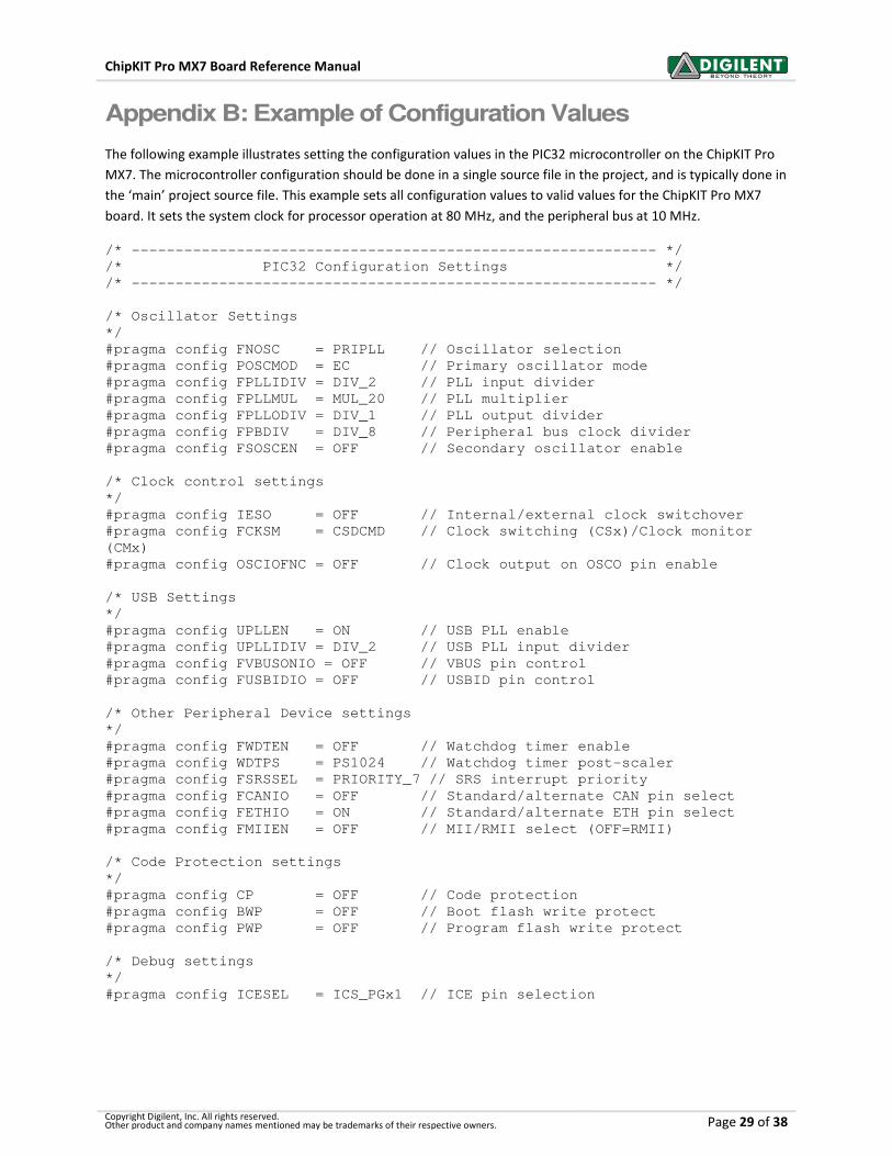
The following example will set up the ChipKIT Pro MX7 for operation with a SYSCLK frequency of 80 MHz and a
PBCLK frequency of 10 MHz:
#pragma config FNOSC = PRIPLL
#pragma config POSCMOD = EC
#pragma config FPLLIDIV = DIV_2
#pragma config FPLLMUL = MUL_20
#pragma config FPLLODIV = DIV_1
#pragma config FPBDIV = DIV_8
Documentation for the PIC32 configuration variables can be found in the PIC32MX Configuration Settings guide.
This is found using the “Help.Topics…” command in the MPLAB IDE. Also, refer to Appendix C for an example of
setting the configuration variables.
When using the ChipKIT Pro MX7 with the MPIDE software, the clock source is set by the boot loader and no action
is required.
6 Ethernet Interface
The ChipKIT Pro MX7 provides the ability to interface with 10Mbps or 100Mbps Ethernet networks. The
PIC32MX795 microcontroller contains a 10/100 Ethernet Medium Access Controller (MAC). External to the PIC32
microcontroller, the ChipKIT Pro MX7 board provides an SMSC LAN8720 Ethernet Physical Layer Transceiver (PHY).
Together, the MAC and PHY in combination with an appropriate coupling transformer and RJ45 jack provide a
standard 10/100 Ethernet interface.
The RJ45 connector J11 provides the physical connection to an Ethernet network using a standard Ethernet cable.
Page 14
ChipKIT Pro MX7 Board Reference Manual
Copyright Digilent, Inc. All rights reserved. Other product and company names mentioned may be trademarks of their respective owners. Page 14 of 38
All devices on an Ethernet network must have a unique address. This address is used to direct packets on the
network to a specific device and to identify the device that originated a packet. An Ethernet MAC uses a 48-bit
address value, commonly called the “MAC Address”. These address values are globally unique to ensure that no
two devices on a network can have conflicting addresses. MAC addresses are assigned by the IEEE. Each
PIC32MX795 device is programmed at the factory to have a unique MAC address that will be loaded by default
when the device is reset.
Digilent provides another unique MAC address that can be used as well. This address is printed on a sticker
attached to the bottom of the board. The Digilent provided MAC address is a twelve digit hexadecimal number of
the form: 00183Exxxxxx, where xxxxxx represents six hexadecimal digits. This value is used to initialize the Ethernet
Controller MAC Station Address registers in the Ethernet controller of the PIC32MX795 microcontroller.
In order to connect to and operate with an Ethernet network, the PIC32 microcontroller must be running network
protocol stack firmware. Normally, the TCP/IP (Transmission Control Protocol/Internet Protocol) network protocol
is used and “TCP/IP Stack” software must be used. The Microchip Applications Library, available for download from
the Microchip web site, provides full protocol stack support compatible with the PIC32MX795 MAC and the
LAN8720 PHY. Microchip also provides numerous example programs illustrating the use of their network protocol
stack for various applications.
When not using the Microchip network protocol stack, refer to the manufacturer documentation for the
PIC32MX795 and LAN8720, plus network protocol documentation, for operation of the Ethernet interface.
Digilent has Network libraries available that can be used to develop both client and server applications when using
the board with the MPIDE development environment. These libraries are built on a custom version of the
Microchip Applications Library network stack and support various network protocols such as TCP, UDP, DHCP and
others to provide complete Ethernet network support. These libraries can be downloaded from the ChipKIT Pro
MX7 product page on the Digilent web site.
The Digilent chipKIT libraries contain examples illustrating various network applications.
The PIC32MX795 microcontroller provides two alternate sets of pins that can be used to connect the MAC to the
external PHY. It also provides two alternate standard MAC/PHY interface signaling conventions. The ChipKIT Pro
MX7 is designed to use the standard (not the alternate) pins, and to use the RMII (not the MII) interface signaling
convention. These options are selected using the configuration variables in the PIC32 microcontroller and are
specified using the #pragma config statement. To enable the Ethernet controller in the correct configuration,
the following statements must appear in the main program module:
#pragma config FETHIO=ON
#pragma config FMIIEN=OFF
The MPIDE boot loader sets these configuration variables, so no action is necessary when using the MPIDE
software system.
The LAN8720 PHY has a reset signal, labeled NRST in the schematic, used to reset the PHY. This signal is connected
to the TRCLK/RA6 pin on the PIC32 microcontroller. The NRST signal is active low. Configure the microcontroller
pin as an output and drive it low to reset the PHY, or drive it high to allow the PHY to come out of reset and begin
operation. The NRST signal is pulled low on the board, so that the PHY is held in reset by default. To allow the PHY
to operate, this pin must be driven high. This reset operation is not part of the Microchip network protocol stack,
and so driving NRST high must be done before initializing the Microchip network stack.
Page 15
ChipKIT Pro MX7 Board Reference Manual
Copyright Digilent, Inc. All rights reserved. Other product and company names mentioned may be trademarks of their respective owners. Page 15 of 38
The Digilent chipKIT network libraries perform this automatically, and so no action is necessary when using the
board with the MPIDE software system and the Digilent libraries.
7 USB Interface
The PIC32MX795 microcontroller contains a USB 2.0 Compliant, Full Speed Device and On-The-Go (OTG) controller.
This controller provides the following features:
• USB full speed host and device support
• Low speed host support
• USB OTG support
• Endpoint buffering anywhere in system RAM
• Integrated DMA to access system RAM and Flash memory.
The USB controller uses a phased lock loop, PLL, to generate the necessary USB clock frequency from the external
primary oscillator input frequency. By default, this PLL is disabled. In order to use the USB controller, it is necessary
to enable the USB PLL, and set the input divider to the correct value to generate a valid USB clock. The input to the
USB PLL must be 4 MHz. The ChipKIT Pro MX7 provides an 8 MHz clock to the PIC32 microcontroller, so a USB PLL
input divider value of 2 must be used. These parameters are set in the PIC32 microcontroller configuration
registers using the #pragma config statement. The following statements must be used to configure the PIC32
microcontroller for use of the USB controller:
#pragma config UPLLEN = ON
#pragma config UPLLIDIV = DIV_2
When using the MPIDE development environment these will have been set by the boot loader, so no action is
needed.
When operating as a USB device, the ChipKIT Pro MX7 can be used as a self-powered device or as a bus powered
device. To operate as a self-powered device, an external power supply should be connected to one of the external
power connectors (J17 or J18) and a shorting block placed on the “EXT” position of J3. To operate as a bus
powered device, the shorting block should be placed in the USB Device position, “USB”, on J3.
Note that when operating as a bus powered device, the ChipKIT Pro MX7 and all devices connected to it are limited
to using no more than 500mA of current to remain in compliance with the USB specification.
Connector J19 on the bottom of the board in the lower right corner is the Device/OTG connector. This is a standard
USB micro-AB connector. Connect a cable with a micro-A plug (optionally available from Digilent) from this
connector to an available USB port on a PC or USB hub for device operation.
When operating as a USB host, the ChipKIT Pro MX7 must be externally powered. Connect a regulated 5V power
supply to one of the external power connectors (J17, or J18) and ensure that the shorting block is in the, “EXT”
position of J3. The power supply used must be a regulated 5V supply. The ChipKIT Pro MX7 board provides power
to the attached USB device when operating as a host and the USB specification requires the use of a 5V power
supply. NOTE: Providing a voltage greater than 5V can damage the ChipKIT Pro MX7 board and/or the USB device
being used.
Connector J20 on the top of the board in the lower right corner is the USB host connector. This is a standard USB
type A receptacle. USB devices may be connected either directly or through a standard USB cable.
Page 16
ChipKIT Pro MX7 Board Reference Manual
Copyright Digilent, Inc. All rights reserved. Other product and company names mentioned may be trademarks of their respective owners. Page 16 of 38
Jumper JP10 is used to route power to the host connector being used. Place the shorting block in the “A” position
when using the standard USB type A (host) Connector, J20. Place the shorting block in the “MICRO” position for
use with the USB micro-AB (OTG) connector, J19.
When operating as a USB host, the PIC32MX795 microcontroller controls application of power to the connected
device via the VBUSON control pin. The VBUSON signal is connected to the circuit net labeled P32_VBUSON in the
schematic. Bus power is applied to the attached USB device by driving the VBUSON pin high. Power is removed
from the device by driving the VBUSON pin low. The VBUSON pin is accessed via bit 3 of the U1OTGCON register.
The VBUSON pin drives the enable input of a Texas Instruments TPS2051B Current-Limited Power Distribution
Switch to control the application of USB power to the host connector. This switch has over-current detection
capability and provides an over-current fault indication by pulling the signal P32_USBOC low. The over-current
output indication can be monitored via I/O Port D pin 13 (RD13) on the PIC32MX795 microcontroller. This pin can
function as change notification pin 19 (CN19), so that a change notification interrupt can be used to detect the
overcurrent condition.
Details about the operation of the TPS2051B can be obtained from the data sheet available at the Texas
Instruments web site.
The Microchip Applications Library, MAL, available on the Microchip web site contains USB driver code for
implementing either USB host devices or USB function devices. This library contains numerous examples
demonstrating both device and host operation of PIC32 microcontrollers. With minor modification or
configuration, these reference designs are suitable to use for developing USB firmware for the ChipKIT Pro MX7
board.
Digilent has USB libraries available that can be used to develop both USB device and USB host applications when
using the board with the MPIDE development environment. These libraries are built on a custom version of the
Microchip Applications Library and can be downloaded from the ChipKIT Pro MX7 product page on the Digilent
web site.
The Digilent chipKIT libraries contain examples illustrating various USB host and device applications.
8 CAN Interface
The Controller Area Network (CAN) is a control networking standard originally developed for use in automobile
systems, but has since become a standard used in various industrial control and building automation networking
applications as well.
The PIC32MX795 microcontroller contains two independent CAN network controllers. These CAN controllers in
combination with two Microchip MCP2551 CAN transceivers allow the ChipKIT Pro MX7 board to operate on up to
two independent CAN networks. Refer to the PIC32MX5XX/6XX/7XX Family Data Sheet and the PIC32 Family
Reference Manual, Section 34, Controller Area Network (CAN), plus CAN network documentation for information
on operation of the CAN controllers and CAN networking in general.
The Microchip C32 peripheral library, plib, provides basic support for all CAN operations using the CAN controllers
in the PIC32MX795 microcontroller.
Digilent has a basic CAN library available for use with the MPIDE software environment. This library can be
downloaded from the ChipKIT Pro MX7 product page on the Digilent web site.
Page 17
ChipKIT Pro MX7 Board Reference Manual
Copyright Digilent, Inc. All rights reserved. Other product and company names mentioned may be trademarks of their respective owners. Page 17 of 38
The PIC32MX795 microcontroller provides two sets of pins that can be used to connect the CAN controllers to the
external transceivers. The ChipKIT Pro MX7 is designed to use the alternate (not the standard) pins. This selection
is made using the configuration variables in the microcontroller, set using a #pragma config statement. To
select the use of the alternate interface pins, the following statement must appear in the main program module:
#pragma config FCANIO=OFF
The MPIDE boot loader sets the configuration variables, and so no action is necessary when using the MPIDE
software system.
The pins on the PIC32MX795 microcontroller used by signals for the CAN1 controller to connect to its transceiver
are shared with two of the signals for the UART2 and SPI4 ports. Jumpers JP1 and JP2 are used to select the use of
these two signals. Place JP1 and JP2 in the CAN position for use of the CAN1 network interface. Place JP1 and JP2 in
the PMOD position for use of these signals for UART or SPI operation. These signals connect to pins 1 & 4 of Pmod
connector JF. When JP1 and JP2 are in the CAN position, Pins 1 & 4 of Pmod connector JF are not useable. In some
cases it may be possible to use UART2 at the same time as CAN1 as the RX and TX pins are not used by the CAN
interface (only RTS and CTS are used). When JP1 and JP2 are in the CAN position Pmod pins JF-01 and JF-04 are not
connected to the PIC32 microcontroller.
There is no standard connector for use with CAN networks. The ChipKIT Pro MX7 board provides two 2x6 pin
header connectors for access to the CAN signals. Connector J9 provides access to the signals for the CAN1 network
controller, and connector J10 provides access to the signals for CAN2. Refer to the ChipKIT Pro MX7 schematic,
Sheet 6, for information on the connectors and signal assignments. Digilent 6-pin or 2x6 to dual 6-pin cables can be
used to daisy chain Digilent boards together in a CAN network. A Digilent 6-Pin cable in combination with a Digilent
PmodCON1 Screw Terminal Connector module can be used to connect the ChipKIT Pro MX7 board to other
network wiring configurations.
The CAN network standard requires that the network nodes at each end of a network provide 120 ohm
termination. The ChipKIT Pro MX7 provides termination resistors and jumpers to enable/disable them depending
on the location of the board in the network. Jumper JP5 is used to enable/disable the termination resistor for the
CAN1 network connector, and JP7 is used to enable/disable the termination resistor for CAN2. Install a shorting
block on the jumper pins to enable the termination resistor, or remove the shorting block to disable it.
9 UART Interface
The PIC32MX795 microcontroller can provide up to six UARTs. Due to conflicting uses of many of the pins used by
the UARTs, the ChipKIT Pro MX7 is designed to allow use of two of them: UART1 and UART2. The UARTs can
provide either a 2-wire or a 4-wire asynchronous serial interface. The 2-wire interface provides receive (RX) and
transmit (TX) pins. The 4-wire interface includes request-to-send (RTS), and clear-to-send (CTS), in addition to
receive and transmit.
UART1 can be accessed from Pmod connector JE and UART2 can be accessed from Pmod connector JF using the
following pins:
• U1CTS JE-01
• U1TX JE-02
• U1RX JE-03
• U1RTS JE-04
Page 18
ChipKIT Pro MX7 Board Reference Manual
Copyright Digilent, Inc. All rights reserved. Other product and company names mentioned may be trademarks of their respective owners. Page 18 of 38
• U2CTS JF-01
• U2TX JF-02
• U2RX JF-03
• U2RTS JF-04
Note that early versions of the Microchip PIC32MX5XX/6XX/7XX Family Data Sheet refer to UART1 as UART1A and
UART2 as UART3A.
Detailed information about the operation of the UART peripherals can be found in the PIC32 Family Reference
Manual, Section 21, UART.
The USB Serial converter is connected to UART1. The MPIDE uses this to communicate with the boot loader. This
can also be used for a serial communications interface between the ChipKIT Pro MX7 board and other software
running on a PC. Resistors are used to decouple the USB serial interface and so UART1 can also be used via Pmod
connector JE when not using it to communicate with the USB serial converter.
Note that when using the MPIDE software, devices connected to JE can interfere with the operation of the serial
interface and prevent the MPIDE from successfully downloading sketches to the board. If this happens, disconnect
the external device from JE until the sketch has been downloaded and then reconnect it.
When using the ChipKIT Pro MX7 with the MPIDE and the chipKIT system, the UARTs are accessed using the
HardwareSerial facility built into the system. UART1 Pmod connector JE, is accessed using the Serial object and
UART2 Pmod connector JF, is accessed using Serial1.
10 Serial Peripheral Interface (SPI)
SPI is a four wire synchronous serial interface and SPI devices can operate as either master devices or as slave
devices. The PIC32 microcontroller labels the four SPI signals as Slave Select (SS), Serial Data Out (SDO), Serial Data
In (SDI), and Serial Clock (SCK). A master device transmits SS, SDO, SCK, and receives SDI. A slave device receives SS,
SDI, SCK, and transmits SDO. The SS signal is used to enable the slave device, and this signal is only significant for
slave devices. A master device can use any general purpose I/O pin to generate SS to enable the slave.
An SPI transaction begins with the master device bringing SS low. When the slave sees SS go low it becomes
enabled and waits for the master to send data. The master shifts data out on SDO and simultaneously shifts data in
on SDI. The slave device receives data from the master on its SDI pin and simultaneously sends data to the master
on its SDO pin. Each time the master sends a byte to the slave, it simultaneously receives a byte from the slave.
The PIC32MX795 microcontroller provides four Serial Peripheral Interfaces. The ChipKIT Pro MX7 supports use of
three ports: SPI1, SPI3, and SPI4. These are accessed using Pmod connectors JD, JE, and JF.
The following gives the mapping between SPI signals and connector pins:
• SS1 JD-01
• SDO1 JD-02
• SDI1 JD-03
• SCK1 JD-04
• SS3 JE-01
• SDO3 JE-02
Page 19
ChipKIT Pro MX7 Board Reference Manual
Copyright Digilent, Inc. All rights reserved. Other product and company names mentioned may be trademarks of their respective owners. Page 19 of 38
• SDI3 JE-03
• SCK3 JE-04
• SS4 JF-01
• SDO4 JF-02
• SDI4 JF-03
• SCK4 JF-04
Note that early versions of the Microchip PIC32MX5Xx/6XX/7XX Family Data Sheet refer to SPI3 as SPI1A and SPI4
as SPI3A.
Detailed information about the operation of the SPI peripherals can be found in the PIC32 Family Reference
Manual, Section 23, Serial Peripheral Interface.
When using the ChipKIT Pro MX7 with the MPIDE and the chipKIT system, the SPI ports are accessed using either
the standard chipKIT SPI library or using the Digilent DSPI library.
The standard SPI library supports access to a single SPI port, SPI4, Pmod connector JF. This is accessed using the
SPI object.
The DSPI library supports access to all three SPI ports. The DSPI0 object class is used to create an object used to
access SPI1, Pmod connector JD. The DSPI1 object class is used to access SPI3, Pmod connector JE, and the
DSPI2 object class is used to access SPI4, Pmod connector JF. I2C™ Interface
11 I2C™ Interface
The Inter-Integrated Circuit (I2C
TM) Interface provides a medium speed (100K or 400K bps) synchronous serial
communications bus. The I2C interface provides master and slave operation using either 7 bit or 10 bit device
addressing. Each device is given a unique address, and the protocol provides the ability to address packets to a
specific device or to broadcast packets to all devices on the bus. Refer to the Microchip PIC32MX5XX/6XX/7XX
Family Data Sheet and the PIC32 Family Reference Manual, Section 24, Inter-Integrated Circuit, for detailed
information on configuring and using the I2C interface.
The PIC32MX795 microcontroller provides for up to five independent I2C interfaces. The ChipKIT Pro MX7 is
designed to provide dedicated access to two of these interfaces I2C1 and I2C2 via I2C daisy chain connectors J7 and
J8. Connector J7 provides access to I2C1 while connector J8 provides access to I2C2.
In addition to I2C1 and I2C2, two other I2C interfaces, I2C3 and I2C5 can be accessed via pins on Pmod connectors.
I2C3 can be accessed via Pmod connector JE, pins JE-02 (SCL3) and JE-03 (SDA3). I2C5 can be accessed via Pmod
connector JF, pins JF-02 (SCL5) and JF-03 (SDA5)
The I2C daisy chain connectors, J7 and J8, each provide two positions for connecting to the I
2C signals, power and
ground. By using two-wire or four-wire MTE cables (available separately from Digilent) a daisy chain of multiple
ChipKIT Pro MX7 boards or other I2C-capable boards can be created.
The I2C bus is an open-collector bus. Devices on the bus actively drive the signals low. The high state on the I
2C
signals is achieved by pull-up resistors when no device is driving the lines low. One device on the I2C bus must
provide the pull-up resistors.
Page 20
ChipKIT Pro MX7 Board Reference Manual
Copyright Digilent, Inc. All rights reserved. Other product and company names mentioned may be trademarks of their respective owners. Page 20 of 38
On the ChipKIT Pro MX7 I2C2, connector J8, has permanently connected 2.2K ohm, pull-up resistors. I2C1,
connector J7, provides selectable pull-ups that can be enabled or disabled via jumper blocks JP3 and JP4. The pull-
ups are enabled by installing shorting blocks on JP3 and JP4. They are disabled by removing the shorting blocks.
Only one device on the bus should have the pull-ups enabled.
If the I2C interfaces on Pmod connectors JE or JF are being used, external pull-up resistors must be provided. These
resistors can be in the range 1K ohm to 10K ohm, and should be connected to pull the pins to 3.3V.
The pull-ups on I2C1 on the ChipKIT Pro MX7 board are actually implemented using current mirrors rather than
simple resistors. These current mirrors source approximately 1.7mA. The use of current mirrors provides faster rise
times on the I2C signals and provides the ability to drive longer cable runs reliably than would be the case with
simple pull-up resistors.
When using the ChipKIT Pro MX7 with the MPIDE and the chipKIT system, the I2C interfaces are accessed using the
standard chipKIT Wire library, or the Digilent DTWI library.
The Wire library supports a single I2C interface, I2C2 on J8. This is accessed using the Wire object.
The DTWI library supports four I2C interfaces. The DTWI0 object class is used to create an object for access to I2C1,
connector J7, and the DTWI1 object class is used to access I2C2, connector J8. The DTWI2 object class is used to
access I2C3, Pmod connector JE, and the DTWI3 object class is used to access I2C5, Pmod connector JF.
The pinouts of the I2C connectors are as follows:
Connector J7 – I2C1
• J7-1, J7-2 – SCL1
• J7-3, J7-4 – SDA1
• J7-5, J7-6 – GND
• J7-7, J7-8 – VCC3V3
Connector J8 – I2C2
• J8-1, J8-2 – SCL2
• J8-3, J8-4 – SDA2
• J8-5, J8-6 – GND
Jumper Settings for I2C Pull-Up Resistor
Page 21
ChipKIT Pro MX7 Board Reference Manual
Copyright Digilent, Inc. All rights reserved. Other product and company names mentioned may be trademarks of their respective owners. Page 21 of 38
• J8-7, J8-8 – VCC3V3
Pmod connector JE – I2C3
• JE-02 – SCL3
• JE-03 – SDA3
Pmod connector JF – I2C5
• JF-02 – SCL5
• JF-03 – SDA5
11.1 On-Board I2C Peripheral Device
The ChipKIT Pro MX7 provides one on-board I2C peripheral device, a Microchip 24LC256 serial EEPROM. This
device is connected to I2C2. The 24LC256 is a 256Kbit (32Kbyte) serial EEPROM device to provide non-volatile
memory storage. The device address for the 24LC256 is 1010000 (0x50).
When using the MPIDE software, this device can be accessed using the Wire library Wire object, or using the
DTWI library via the DTWI1 object class.
Refer to the Microchip data sheet for detailed information on the operation of this device.
12 Analog Inputs
The PIC32MX795 microcontroller provides a 10-bit analog to digital (A/D) converter that provides up to sixteen
analog inputs. The ChipKIT Pro MX7 board provides access to 10 of these inputs via the Pmod connectors. The
converted values produced by the A/D converter will be in the range 0–1023.
For detailed information on the operation and use of the A/D converter, refer to the PIC32 Family Reference
Manual, Section 17, 10-bit AD Converter.
The analog inputs are accessed using the analogRead() function in the MPIDE software. The analog input pin
number is specified using the symbols A0–A9. The digital pin numbers for the pins or the numbers 0–9 can also be
used, but using the symbols A0–A9 is recommended.
The following gives the Pmod connector position, digital pin number, microcontroller I/O port, and bit number for
the analog inputs:
• A0 – JA-01, digital pin 0, RB02
• A1 – JA-02, digital pin 1, RB03
• A2 – JA-03, digital pin 2, RB04
• A3 – JA-04, digital pin 3, RB06
• A4 – JA-07, digital pin 4, RB07
• A5 – JA-08, digital pin 5, RB08
• A6 – JA-09, digital pin 6, RB09
• A7 – JA-10, digital pin 7, RB10
• A8 – JC-07, digital pin 20, RB15
• A9 – JC-10, digital pin 23, RB14
Page 22
ChipKIT Pro MX7 Board Reference Manual
Copyright Digilent, Inc. All rights reserved. Other product and company names mentioned may be trademarks of their respective owners. Page 22 of 38
12.1 A/D Converter Voltage Reference
The PIC32 microcontroller provides two voltage reference inputs to the analog to digital converter. Vref- is used
set the lower reference level and Vref+ is used to set the upper reference level. These references can be connected
to internal references or to external references using two of the analog input pins.
When the internal references are being used, Vref- is connected to VSS and Vref+ is connected to VDD. This means
that the voltage input range at the analog input pins is 0V–3.3V. In this case, an input voltage of 0V will convert to
~0, an input voltage of 1.65V will convert to ~511, and an input voltage of 3.3V will convert to ~1023.
Either one, or both, of the references can be connected to external reference pins. When this is done, the
references can be set to voltages other than 0V and 3.3V.
If, for example, both references were selected to use external references, with 1V applied to Vref- and 2V applied
to Vref+, the input voltage range at the analog input pins would be from 1V to 2V. An applied voltage of 1V would
have a converted value of ~0, 1.5V would have a converted value of ~511, and 2V would have a converted value of
~1023.
When both external references are being used, Vref+ must have a higher voltage applied to in than Vref-.
The analog reference input pins appear on Pmod connector JE, pins 9 & 10. Vref- is on pin JE-09, and Vref+ is on
pin JE-10. These pins are not available to be used for digital I/O when being used as an external reference.
When using the MPIDE software, the use of external analog references is selected using the analogReference()
function. The following values can be used with analogReference():
• DEFAULT – Vref- = 0V, Vref+ = 3.3V
• INTERNAL – same as default
• EXTERNAL – Vref- = 0V, Vref+ = voltage at A2
• EXTMINUS – Vref- = voltage at A3, Vref+ = 3.3V
• EXTPLUSMINUS – Vref- = voltage at A3, Vref+ = voltage at A2
13 Timers
The PIC32MX795 microcontroller provides five timers that can be used for various timing functions. These timers
are each 16 bits wide, although two pairs, TIMER2/TIMER3 and TIMER4/TIMER5 can be combined to produce 32
bit wide timers.
A timer consists of a control register, a counter register, and a period register. The control register is used to
configure the timer for various modes of operation. The count register counts cycles of the clock source selected
via the control register. This clock source can be the peripheral bus clock or a division of the peripheral bus clock
via a prescaler divider. The period register can be used to generate an interrupt and/or reset the count register
when a predetermined value is reached.
Each timer has an associated input pin. In some operating modes, this pin can be used as an external clock input to
the timer, or as a gate input to turn on/off incrementing of the counter register under control of an external signal.
The following gives the Pmod connector position, chipKIT pin number, microcontroller I/O port, and bit number for
the timer input pins.
• T1CK – not available
• T2CK – JC-01, digital pin 16, RC01
Page 23
ChipKIT Pro MX7 Board Reference Manual
Copyright Digilent, Inc. All rights reserved. Other product and company names mentioned may be trademarks of their respective owners. Page 23 of 38
• T3CK – not available
• T4CK – not available
• T5CK – JD-03, digital pin 26, RC04
For detailed information on the operation of the PIC32 timers, refer to the PIC32 Family Reference Manual, Section
14, Timers.
When using the MPIDE software, the symbols PIN_TCK2 and PIN_TCK5 can be used to access the timer input pins.
Control and operation of the timers is not explicitly provided in the current version of the MPIDE software. This
capability will be added in a future version of the software; however, timers are used implicitly by various core
functions and libraries.
14 Output Compare
The PIC32MX795 microcontroller provides five output compare units that can be used to control the timing of
state changes on certain output pins or to generate pulse width modulated (PWM) outputs.
Each output compare unit works with a particular output pin (OC1-OC5). It can be programmed to control the pin
in any of the following ways:
• PWM output
• Generate continuous pulses
• Generate a single pulse
• Toggle the output pin
• Generate falling edge
• Generate rising edge
The output compare units work in conjunction with a timer. Either Timer2 or Timer3 can be used with any of the
five output compare units.
Refer to the PIC32 Family Reference Manual, Section 16, Output Compare for detailed information on the use of
the output compare units.
When using the MPIDE software, these are accessed using the analogWrite() function. The digital pin number, or
preferably, the symbols PIN_OC1 through PIN_OC5 are used to specify the pin. The MPIDE software currently only
supports using the output compare units to generate PWM outputs. It uses Timer2 to control the output
compares.
The following gives Pmod connector position, chipKIT pin number, and microcontroller I/O port and bit number for
the output compare unit’s output pins:
• OC1 – JD-02, digital pin 25, RD00
• OC2 – JD-07, digital pin 28, RD01
• OC3 – JD-08, digital pin 29, RD02
• OC4 – JD-09, digital pin 30, RD03
• OC5 – JC-09, digital pin 22, RD04
15 Input Capture
The PIC32MX795 microcontroller provides five input capture units. The design of the ChipKIT Pro MX7 board
allows the use of three of them.
Page 24
ChipKIT Pro MX7 Board Reference Manual
Copyright Digilent, Inc. All rights reserved. Other product and company names mentioned may be trademarks of their respective owners. Page 24 of 38
An input capture unit works in conjunction with a timer and monitors the state of an associated pin. When the pin
changes state, the current value of the timer is captured. The input capture units can be used with either Timer2 or
Timer3.
The input capture unit can be programmed to be sensitive to either a rising edge, a falling edge, or both edges on
the input pin. An interrupt can also be signaled when an input capture is triggered. Each input capture has a four
level deep FIFO that can buffer up to four capture events.
For detailed information on the operation and use of the input capture units, refer to the PIC32 Family Reference
Manual, Section 15, Input Capture.
The following gives the Pmod connector position, chipKIT pin number, and microcontroller port and bit number for
the input capture units input pins:
• IC1 – not available
• IC2 – JD-01, digital pin 24, RD09
• IC3 – JD-04, digital pin 27, RD10
• IC4 – not available
• IC5 – JD-10, digital pin 31, RD12
When using the MPIDE software, the symbols PIN_IC2, PIN_IC3, and PIN_IC5 can be used to access the capture
input pins.
Use of the input capture units is not currently supported in the MPIDE software. This will be added in a future
version.
16 External Interrupts
The PIC32 microcontroller provides five external interrupt inputs. An external interrupt input can be used to
generate an interrupt to the microprocessor CPU when the pin changes state. They can be programmed to
interrupt on a rising edge or a falling edge on the pin.
Refer to the PIC32 Family Reference Manual, Section 8, Interrupts for more information on the operation of the
external interrupts.
These are accessed using the attachInterrupt() and detachInterrupt() functions when using the MPIDE software.
The interrupt number is specified using the numbers 0-4, or preferably, the symbols EXT_INT0 through EXT_INT4.
The symbols PIN_INT0 through PIN_INT4 are also defined to refer to the digital pin numbers used for the external
interrupt inputs.
The following gives connector position, chipKIT pin number, and microcontroller I/O port and bit number. Note
that INT0-INT1 are on Pmod connectors. INT3 and INT4 are on I2C1 daisy chain connector J7. When using these
pins as external interrupt inputs, they are not available to use for I2C. It may also be necessary to disable the pull-
ups by pulling the shorting blocks from JP3 or JP4.
• INT0 – JD-02, digital pin 25, RD00
• INT1 – JE-07, digital pin 36, RE08
• INT2 – JF-07, digital pin 44, RE09
• INT3 – J7-1 & J7-2, digital pin 57, RA14
• INT4 – J7-3 & J7-4, digital pin 58, RA15
Page 25
ChipKIT Pro MX7 Board Reference Manual
Copyright Digilent, Inc. All rights reserved. Other product and company names mentioned may be trademarks of their respective owners. Page 25 of 38
17 RTCC
The PIC32 microcontroller contains a low frequency oscillator and Real Time Clock/Calendar circuit, RTCC, which
can be used to maintain time and date information. The operation of the RTCC requires a 32.768 KHz frequency
source. The crystal X2 position, just above and on the right of the PIC32 microcontroller, IC1, is provided for the
user to solder in a 32 KHz watch crystal. The Citizen CFS206-32.768KDZF-UB is a crystal part that can be used in this
location.
Page 26
ChipKIT Pro MX7 Board Reference Manual
Copyright Digilent, Inc. All rights reserved. Other product and company names mentioned may be trademarks of their respective owners. Page 26 of 38
Appendix A: Connector Descriptions and Jumper Settings
Label Function
JA-JF
Pmod Connectors
These connectors provide access to the I/O pins on the PIC32MX795 microcontroller. Digilent Pmod peripheral
modules can be attached to these connectors. These connectors can be used for general access to I/O pins on
the PIC32MX795 microcontroller.
JPA –
JPF
Pmod header power select
Any of the Pmod connectors can provide either regulated or unregulated power. To use regulated power, place
the jumper block over the center pin and the pin marked 3V3. To use unregulated power, place the jumper
block over the center pin and the pin marked 5V0.
J1
USB Serial converter auxiliary signals
This connector can be used to access the auxiliary RS232 handshaking signals not used on the ChipKIT MX4
board.
J2
USB Serial converter (UART) connector
This USB micro-AB connector is used to connect the FT232R serial converter to a USB port on the user PC.
J3
Power supply source select
This jumper is used to select the source of main board power.
Place the shorting block in the “USB” position to have the board powered from the USB device connector, J19.
Place the shorting block in the “EXT” position to have the board powered from one of the external power
connectors, J17 or J18.
Place the shorting block in the “DBG” position to have the board powered from the debug USB connector, J15.
Place the shorting block in the “UART” position to have the board powered from the USB serial converter
connector, J2
J7
I2C1 daisy chain connector
This connector provides access to the I2C signals, power, and ground for I2C1.
J8
I2C2 daisy chain connector
This connector provides access to the I2C signals, power, and ground for I2C2.
J9
CAN #1 Connector
This connector is used to access the signals for CAN #1.
J10
CAN #2 Connector
This connector is used to access the signals for CAN #2.
J11
Ethernet Connector
This connector provides access to the 10/100 Ethernet port.
J12-J14 Do Not Use.
J15 Debug USB Connector
Page 27
ChipKIT Pro MX7 Board Reference Manual
Copyright Digilent, Inc. All rights reserved. Other product and company names mentioned may be trademarks of their respective owners. Page 27 of 38
This connector is used to connect the on-board programming and debug circuit to the PC for use with the
MPLAB IDE.
J17
External Power Connector
This is a 2.5mm x 5.5mm, center positive, coax power connector used to provide external power to the board.
The optional Digilent 5V Switching Power Supply is connected here.
J18
External Power Connector
This is a screw terminal connector used to provide external power to the board. Be sure to observe proper
polarity (marked near the connector) when providing power via this connector, or damage to the board and/or
connected devices may result.
J19
USB Device / OTG Connector
This is a USB micro-AB connector. It is used when using the PIC32MX795 microcontroller to implement a USB
device or OTG Host/Device.
J20
USB Host Connector
This is a standard sized USB type A connector. This connector is used to connect USB devices to the board when
using the PIC32MX795 microcontroller to implement an embedded USB host.
JP1 &
JP2
CAN or Pmod Select
These jumpers select microcontroller signals RF12 and RF13 for use with CAN #1 or Pmod connector JF. Place
these jumpers in the CAN position to use CAN #1. Place the jumpers in the PMOD position to use then with
Pmod connector JF.
JP3 &
JP4
Pull-up enable for I2C1
These two jumpers are used to enable/disable the pull-up resistors on I2C1. Insert shorting blocks on these two
jumpers to enable the pull-up resistors. Remove the shorting blocks to disable the pull-up resistors. Only a
single device on the I2C bus should have the pull-up resistors enabled.
JP5
CAN #1 Termination
This jumper is used to enable/disable the 120 ohm termination resistor for CAN #1. Insert the shorting block to
enable the termination resistor, remove it to disable the termination resistor.
JP6
CAN #1 5V0 Enable
This jumper is used to enable/disable providing 5V to the CAN #1 connector. Insert the shorting block to
connect the board 5V0 supply to pins 9 & 10 of CAN #1 connector. Remove the shorting block to disconnect the
5V0 supply.
JP7
CAN #2 Termination
This jumper is used to enable/disable the 120 ohm termination resistor for CAN #2. Insert the shorting block to
enable the termination resistor, remove it to disable the termination resistor.
JP8
CAN #1 5V0 Enable
This jumper is used to enable/disable providing 5V to the CAN #1 connector. Insert the shorting block to
connect the board 5V0 supply to pins 9 & 10 of CAN #1 connector. Remove the shorting block to disconnect the
5V0 supply.
JP9 Do Not Use.
JP10
USB host power select
This jumper is used to select which host connector is powered when host power is enabled. Place the shorting
block in the “MICRO” position to supply power to the USB micro-AB OTG Connector, J19. Place the shorting
block in the “A” position to supply power to the USB type A Host Connector, J20.
Page 28
ChipKIT Pro MX7 Board Reference Manual
Copyright Digilent, Inc. All rights reserved. Other product and company names mentioned may be trademarks of their respective owners. Page 28 of 38
JP11
USB Serial converter reset disconnect
This is used to connect/disconnect the USB serial converter reset circuit from the PIC32 MCLR pin. The shorting
block must be in place on this jumper when using the MPIDE development tools. Remove the shorting block if
the USB serial converter is interfering with proper operation of the licensed debugger circuit.
JP17 Do Not Use.
Page 29
ChipKIT Pro MX7 Board Reference Manual
Copyright Digilent, Inc. All rights reserved. Other product and company names mentioned may be trademarks of their respective owners. Page 29 of 38
Appendix B: Example of Configuration Values
The following example illustrates setting the configuration values in the PIC32 microcontroller on the ChipKIT Pro
MX7. The microcontroller configuration should be done in a single source file in the project, and is typically done in
the ‘main’ project source file. This example sets all configuration values to valid values for the ChipKIT Pro MX7
board. It sets the system clock for processor operation at 80 MHz, and the peripheral bus at 10 MHz.
/* ------------------------------------------------------------ */
/* PIC32 Configuration Settings */
/* ------------------------------------------------------------ */
/* Oscillator Settings
*/
#pragma config FNOSC = PRIPLL // Oscillator selection
#pragma config POSCMOD = EC // Primary oscillator mode
#pragma config FPLLIDIV = DIV_2 // PLL input divider
#pragma config FPLLMUL = MUL_20 // PLL multiplier
#pragma config FPLLODIV = DIV_1 // PLL output divider
#pragma config FPBDIV = DIV_8 // Peripheral bus clock divider
#pragma config FSOSCEN = OFF // Secondary oscillator enable
/* Clock control settings
*/
#pragma config IESO = OFF // Internal/external clock switchover
#pragma config FCKSM = CSDCMD // Clock switching (CSx)/Clock monitor
(CMx)
#pragma config OSCIOFNC = OFF // Clock output on OSCO pin enable
/* USB Settings
*/
#pragma config UPLLEN = ON // USB PLL enable
#pragma config UPLLIDIV = DIV_2 // USB PLL input divider
#pragma config FVBUSONIO = OFF // VBUS pin control
#pragma config FUSBIDIO = OFF // USBID pin control
/* Other Peripheral Device settings
*/
#pragma config FWDTEN = OFF // Watchdog timer enable
#pragma config WDTPS = PS1024 // Watchdog timer post-scaler
#pragma config FSRSSEL = PRIORITY_7 // SRS interrupt priority
#pragma config FCANIO = OFF // Standard/alternate CAN pin select
#pragma config FETHIO = ON // Standard/alternate ETH pin select
#pragma config FMIIEN = OFF // MII/RMII select (OFF=RMII)
/* Code Protection settings
*/
#pragma config CP = OFF // Code protection
#pragma config BWP = OFF // Boot flash write protect
#pragma config PWP = OFF // Program flash write protect
/* Debug settings
*/
#pragma config ICESEL = ICS_PGx1 // ICE pin selection
Page 30
ChipKIT Pro MX7 Board Reference Manual
Copyright Digilent, Inc. All rights reserved. Other product and company names mentioned may be trademarks of their respective owners. Page 30 of 38
Appendix C: Connector Pinout Tables
Arranged by Microcontroller Pin Number
PIC32
Pin #
Connector
Pin
chipKIT
Pin #
MCU
Port Bit PIC32 Signal Name Notes
1 LD4 54 RG15 AERXERR/RG15 LED4
3 JB-08 14 RE05 PMD5/RE5
4 JB-09 15 RE06 PMD6/RE6
5 JB-10 16 RE07 PMD7/RE7
6 JC-01 17 RC01 T2CK/RC1
7 N/A N/A RC02 T3CK/AC2TX/RC2 CAN2
8 N/A N/A RC03 T4CK/AC2RX/RC3 CAN2
9 JD-03 27 RC04 T5CK/SDI1/RC4
10 BTN1 48 RG06 .../SCK2A/U2BTX/U2ARTS/PMA5/CN8/RG6 BTN1
11 BTN2 49 RG07 .../SDA2A/SDI2A/U2ARX/PMA4/CN9/RG7 BTN2
12 N/A N/A RG08 .../SCL2A/SDO2A/U2ATX/PMA3/CN10/RG8 Ethernet PHY
14 N/A N/A RG09 .../SS2A/U2BRX/U2ACTS/PMA2/CN11/RG9 Ethernet PHY
17 BTN3 50 RA00 TMS/RA0 BTN3
18 JE-07 37 RE08 AERXD0/INT1/RE8
19 JF-07 45 RE09 AERXD1/INT2/RE9
20 N/A 59 RB05 AN5/C1IN+/VBUSON/CN7/RB5 USB VBUSON
21 JA-03 3 RB04 AN4/C1IN-/CN6/RB4
22 JA-02 2 RB03 AN3/C2IN+/CN5/RB3
23 JA-01 1 RB02 AN2/C2IN-/CN4/RB2
24 N/A N/A RB01 PGEC1/AN1/CN3/RB1 debug PGD
25 N/A N/A RB00 PGED1/AN0/CN2/RB0 debug PGC
26 JA-04 4 RB06 PGEC2/AN6/OCFA/RB6
27 JA-07 5 RB07 PGED2/AN7/RB7
28 JE-09 39 RA09 Vref-/CVref-/AERXD2/PMA7/RA9
29 JE-10 40 RA10 Vref+/CVref+/AERXD3/PMA6/RA10
32 JA-08 6 RB08 AN8/C1OUT/RB8
33 JA-09 7 RB09 AN9/C2OUT/RB9
34 JA-10 8 RB10 CVrefout/PMA13/AN10/RB10
35 N/A N/A RB11 AN11/ERXERR/AETXERR/PMA12/RB11 Ethernet PHY
38 JF-08 46 RA01 TCK/RA1
39 JF-04 44 RF13 AC1TX/SCK3A/U3BTX/U3ARTS/RF13 also CAN1 (JP-2)
40 JF-01 41 RF12 AC1RX/SS3A/U3BRX/U3ACTS/RF12 also CAN1 (JP-1)
41 N/A N/A RB12 AN12/ERXD0/AECRS/PMA11/RB12 Ethernet PHY
42 N/A N/A RB13 AN13/ERXD1/AECOL/PMA10/RB13 Ethernet PHY
43 JC-10 24 RB14 AN14/ERXD2/AETXD3/PMALH/PMA1/RB14
44 JC-07 21 RB15 AN15/.../OCFB/PMALL/PMA0/CN12/RB15
Page 31
ChipKIT Pro MX7 Board Reference Manual
Copyright Digilent, Inc. All rights reserved. Other product and company names mentioned may be trademarks of their respective owners. Page 31 of 38
47 JE-01 33 RD14 AETXD0/SS1A/U1BRX/U1ACTS/CN20/RD14
48 JE-04 36 RD15 AETXD1/SCK1A/U1BTX/U1ARTS/CN21/RD15
49 JF-03 43 RF04 SDA3A/SDI3A/U3ARX/PMA9/CN17/RF4
50 JF-02 42 RF05 SCL3A/SDO3A/U3ATX/PMA8/CN18/RF5
51 N/A N/A RF03 USBID/RF3 USBID (USB-4)
52 JE-03 35 RF02 SDA1A/SDI1A/U1ARX/RF2
53 JE-02 34 RF08 SCL1A/SDO1A/U1ATX/RF8
56 N/A N/A RG03 D-/RG3 D- (USB-2)
57 N/A N/A RG02 D+/RG2 D+ (USB-3)
58 J7-1,J7-2 55 RA02 SCL2/RA2 I2C2
59 J7-3,J7-4 56 RA03 SDA2/RA3 I2C2
60 JF-09 47 RA04 TDI/RA4
61 JF-10 48 RA05 TDO/RA5
63 N/A N/A RC12 OSC1/CLKI/RC12 Primary Oscillator
64 N/A N/A RC15 OSC2/CLKO/RC15 Primary Oscillator
66 J8-1,J8-2 57 RA14 AETXCLK/SCL1/INT3/RA14 I2C1
67 J8-3.J8-4 58 RA15 AETXEN/SDA1/INT4/RA15 I2C1
68 N/A N/A RD08 RTCC/EMDIO/AEMDIO/IC1/RD8 Ethernet PHY
69 JD-01 25 RD09 SS1/IC2/RD9
70 JD-04 28 RD10 SCK1/IC3/PMCS2/PMA15/RD10
71 N/A N/A RD11 EMDC/AEMDC/IC4/PMCS1/PMA14/RD11 Ethernet PHY
72 JD-02 26 RD00 SDO1/OC1/INT0/RD0
73 N/A N/A RC13 SOSCI/CN1/RC13 Secondary Oscillator
74 N/A N/A RC14 SOSCO/T1CK/CN0/RC14 Secondary Oscillator
76 JD-07 29 RD01 OC2/RD1
77 JD-08 30 RD02 OC3/RD2
78 JD-09 31 RD03 OC4/RD3
79 JD-10 32 RD12 ETXD2/IC5/PMD12/RD12
80 N/A 60 RD13 ETXD3/PMD13/CN19/RD13 USB Overcurrent
81 JC-09 23 RD04 OC5/PMWR/CN13/RD4
82 JC-08 22 RD05 PMRD/CN14/RD5
83 N/A N/A RD06 ETXEN/PMD14/CN15/RD6 Ethernet PHY
84 JC-04 20 RD07 ETXCLK/PMD15/CN16/RD7
87 N/A N/A RF00 C1RX/ETXD1/PMD11/RF0 Ethernet PHY
88 N/A N/A RF01 C1TX/ETXD0/PMD10/RF1 Ethernet PHY
89 JC-03 19 RG01 C2TX/ETXERR/PMD9/RG1
90 JC-02 18 RG00 C2RX/PMD8/RG0
91 N/A N/A RA06 TRCLK/RA6 Ethernet PHY Reset
92 JE-08 38 RA07 TRD3/RA7
93 JB-01 9 RE00 PMD0/RE0
94 JB-02 10 RE01 PMD1/RE1
Page 32
ChipKIT Pro MX7 Board Reference Manual
Copyright Digilent, Inc. All rights reserved. Other product and company names mentioned may be trademarks of their respective owners. Page 32 of 38
95 LD3 53 RG14 TRD2/RG14 LED3
96 LD1 51 RG12 TRD1/RG12 LED1
97 LD2 52 RG13 TRD0/RG13 LED2
98 JB-03 11 RE02 PMD2/RE2
99 JB-04 12 RE03 PMD3/RE3
100 JB-07 13 RE04 PMD4/RE4
Page 33
ChipKIT Pro MX7 Board Reference Manual
Copyright Digilent, Inc. All rights reserved. Other product and company names mentioned may be trademarks of their respective owners. Page 33 of 38
Arranged by Connector Pin Number and Digital Pin Number
PIC32
Pin #
Connector
Pin
ChipKIT
Pin #
MCU
Port Bit PIC32 Signal Name Notes
23 JA-01 1 RB02 AN2/C2IN-/CN4/RB2
22 JA-02 2 RB03 AN3/C2IN+/CN5/RB3
21 JA-03 3 RB04 AN4/C1IN-/CN6/RB4
26 JA-04 4 RB06 PGEC2/AN6/OCFA/RB6
27 JA-07 5 RB07 PGED2/AN7/RB7
32 JA-08 6 RB08 AN8/C1OUT/RB8
33 JA-09 7 RB09 AN9/C2OUT/RB9
34 JA-10 8 RB10 CVrefout/PMA13/AN10/RB10
93 JB-01 9 RE00 PMD0/RE0
94 JB-02 10 RE01 PMD1/RE1
98 JB-03 11 RE02 PMD2/RE2
99 JB-04 12 RE03 PMD3/RE3
100 JB-07 13 RE04 PMD4/RE4
3 JB-08 14 RE05 PMD5/RE5
4 JB-09 15 RE06 PMD6/RE6
5 JB-10 16 RE07 PMD7/RE7
6 JC-01 17 RC01 T2CK/RC1
90 JC-02 18 RG00 C2RX/PMD8/RG0
89 JC-03 19 RG01 C2TX/ETXERR/PMD9/RG1
84 JC-04 20 RD07 ETXCLK/PMD15/CN16/RD7
44 JC-07 21 RB15 AN15/.../OCFB/PMALL/PMA0/CN12/RB15
82 JC-08 22 RD05 PMRD/CN14/RD5
81 JC-09 23 RD04 OC5/PMWR/CN13/RD4
43 JC-10 24 RB14 AN14/ERXD2/AETXD3/PMALH/PMA1/RB14
69 JD-01 25 RD09 SS1/IC2/RD9
72 JD-02 26 RD00 SDO1/OC1/INT0/RD0
9 JD-03 27 RC04 T5CK/SDI1/RC4
70 JD-04 28 RD10 SCK1/IC3/PMCS2/PMA15/RD10
76 JD-07 29 RD01 OC2/RD1
77 JD-08 30 RD02 OC3/RD2
78 JD-09 31 RD03 OC4/RD3
79 JD-10 32 RD12 ETXD2/IC5/PMD12/RD12
47 JE-01 33 RD14 AETXD0/SS1A/U1BRX/U1ACTS/CN20/RD14
Page 34
ChipKIT Pro MX7 Board Reference Manual
Copyright Digilent, Inc. All rights reserved. Other product and company names mentioned may be trademarks of their respective owners. Page 34 of 38
53 JE-02 34 RF08 SCL1A/SDO1A/U1ATX/RF8
52 JE-03 35 RF02 SDA1A/SDI1A/U1ARX/RF2
48 JE-04 36 RD15 AETXD1/SCK1A/U1BTX/U1ARTS/CN21/RD15
18 JE-07 37 RE08 AERXD0/INT1/RE8
92 JE-08 38 RA07 TRD3/RA7
28 JE-09 39 RA09 Vref-/CVref-/AERXD2/PMA7/RA9
29 JE-10 40 RA10 Vref+/CVref+/AERXD3/PMA6/RA10
40 JF-01 41 RF12 AC1RX/SS3A/U3BRX/U3ACTS/RF12 also CAN1 (JP-1)
50 JF-02 42 RF05 SCL3A/SDO3A/U3ATX/PMA8/CN18/RF5
49 JF-03 43 RF04 SDA3A/SDI3A/U3ARX/PMA9/CN17/RF4
39 JF-04 44 RF13 AC1TX/SCK3A/U3BTX/U3ARTS/RF13 also CAN1 (JP-2)
19 JF-07 45 RE09 AERXD1/INT2/RE9
38 JF-08 46 RA01 TCK/RA1
60 JF-09 47 RA04 TDI/RA4
10 BTN1 48 RG06 .../SCK2A/U2BTX/U2ARTS/PMA5/CN8/RG6 BTN1
61 JF-10 48 RA05 TDO/RA5
11 BTN2 49 RG07 .../SDA2A/SDI2A/U2ARX/PMA4/CN9/RG7 BTN2
17 BTN3 50 RA00 TMS/RA0 BTN3
96 LD1 51 RG12 TRD1/RG12 LED1
97 LD2 52 RG13 TRD0/RG13 LED2
95 LD3 53 RG14 TRD2/RG14 LED3
1 LD4 54 RG15 AERXERR/RG15 LED4
58 J7-1,J7-2 55 RA02 SCL2/RA2 I2C2
59 J7-3,J7-4 56 RA03 SDA2/RA3 I2C2
66 J8-1,J8-2 57 RA14 AETXCLK/SCL1/INT3/RA14 I2C1
67 J8-3.J8-4 58 RA15 AETXEN/SDA1/INT4/RA15 I2C1
20 N/A 59 RB05 AN5/C1IN+/VBUSON/CN7/RB5 USB VBUSON
80 N/A 60 RD13 ETXD3/PMD13/CN19/RD13 USB Overcurrent detect
7 N/A N/A RC02 T3CK/AC2TX/RC2 CAN2
8 N/A N/A RC03 T4CK/AC2RX/RC3 CAN2
12 N/A N/A RG08 .../SCL2A/SDO2A/U2ATX/PMA3/CN10/RG8 Ethernet PHY
14 N/A N/A RG09 .../SS2A/U2BRX/U2ACTS/PMA2/CN11/RG9 Ethernet PHY
24 N/A N/A RB01 PGEC1/AN1/CN3/RB1 debug PGD
25 N/A N/A RB00 PGED1/AN0/CN2/RB0 debug PGC
35 N/A N/A RB11 AN11/ERXERR/AETXERR/PMA12/RB11 Ethernet PHY
41 N/A N/A RB12 AN12/ERXD0/AECRS/PMA11/RB12 Ethernet PHY
Page 35
ChipKIT Pro MX7 Board Reference Manual
Copyright Digilent, Inc. All rights reserved. Other product and company names mentioned may be trademarks of their respective owners. Page 35 of 38
42 N/A N/A RB13 AN13/ERXD1/AECOL/PMA10/RB13 Ethernet PHY
51 N/A N/A RF03 USBID/RF3 USBID (USB-4)
56 N/A N/A RG03 D-/RG3 D- (USB-2)
57 N/A N/A RG02 D+/RG2 D+ (USB-3)
63 N/A N/A RC12 OSC1/CLKI/RC12 Primary Oscillator
64 N/A N/A RC15 OSC2/CLKO/RC15 Primary Oscillator
68 N/A N/A RD08 RTCC/EMDIO/AEMDIO/IC1/RD8 Ethernet PHY
71 N/A N/A RD11 EMDC/AEMDC/IC4/PMCS1/PMA14/RD11 Ethernet PHY
73 N/A N/A RC13 SOSCI/CN1/RC13 Secondary Oscillator
74 N/A N/A RC14 SOSCO/T1CK/CN0/RC14 Secondary Oscillator
83 N/A N/A RD06 ETXEN/PMD14/CN15/RD6 Ethernet PHY
87 N/A N/A RF00 C1RX/ETXD1/PMD11/RF0 Ethernet PHY
88 N/A N/A RF01 C1TX/ETXD0/PMD10/RF1 Ethernet PHY
91 N/A N/A RA06 TRCLK/RA6 Ethernet PHY Reset
Page 36
ChipKIT Pro MX7 Board Reference Manual
Copyright Digilent, Inc. All rights reserved. Other product and company names mentioned may be trademarks of their respective owners. Page 36 of 38
Arranged by MCU Port and Bit Number
PIC32
Pin #
Connector
Pin
chipKIT
Pin #
MCU
Port Bit PIC32 Signal Name Notes
17 BTN3 50 RA00 TMS/RA0 BTN3
38 JF-08 46 RA01 TCK/RA1
58 J7-1,J7-2 55 RA02 SCL2/RA2 I2C2
59 J7-3,J7-4 56 RA03 SDA2/RA3 I2C2
60 JF-09 47 RA04 TDI/RA4
61 JF-10 48 RA05 TDO/RA5
91 N/A N/A RA06 TRCLK/RA6 Ethernet PHY Reset
92 JE-08 38 RA07 TRD3/RA7
28 JE-09 39 RA09 Vref-/CVref-/AERXD2/PMA7/RA9
29 JE-10 40 RA10 Vref+/CVref+/AERXD3/PMA6/RA10
66 J8-1,J8-2 57 RA14 AETXCLK/SCL1/INT3/RA14 I2C1
67 J8-3.J8-4 58 RA15 AETXEN/SDA1/INT4/RA15 I2C1
25 N/A N/A RB00 PGED1/AN0/CN2/RB0 debug PGC
24 N/A N/A RB01 PGEC1/AN1/CN3/RB1 debug PGD
23 JA-01 1 RB02 AN2/C2IN-/CN4/RB2
22 JA-02 2 RB03 AN3/C2IN+/CN5/RB3
21 JA-03 3 RB04 AN4/C1IN-/CN6/RB4
20 N/A 59 RB05 AN5/C1IN+/VBUSON/CN7/RB5 USB VBUSON
26 JA-04 4 RB06 PGEC2/AN6/OCFA/RB6
27 JA-07 5 RB07 PGED2/AN7/RB7
32 JA-08 6 RB08 AN8/C1OUT/RB8
33 JA-09 7 RB09 AN9/C2OUT/RB9
34 JA-10 8 RB10 CVrefout/PMA13/AN10/RB10
35 N/A N/A RB11 AN11/ERXERR/AETXERR/PMA12/RB11 Ethernet PHY
41 N/A N/A RB12 AN12/ERXD0/AECRS/PMA11/RB12 Ethernet PHY
42 N/A N/A RB13 AN13/ERXD1/AECOL/PMA10/RB13 Ethernet PHY
43 JC-10 24 RB14 AN14/ERXD2/AETXD3/PMALH/PMA1/RB14
44 JC-07 21 RB15 AN15/.../OCFB/PMALL/PMA0/CN12/RB15
6 JC-01 17 RC01 T2CK/RC1
7 N/A N/A RC02 T3CK/AC2TX/RC2 CAN2
Page 37
ChipKIT Pro MX7 Board Reference Manual
Copyright Digilent, Inc. All rights reserved. Other product and company names mentioned may be trademarks of their respective owners. Page 37 of 38
8 N/A N/A RC03 T4CK/AC2RX/RC3 CAN2
9 JD-03 27 RC04 T5CK/SDI1/RC4
63 N/A N/A RC12 OSC1/CLKI/RC12 Primary Oscillator
73 N/A N/A RC13 SOSCI/CN1/RC13 Secondary Oscillator
74 N/A N/A RC14 SOSCO/T1CK/CN0/RC14 Secondary Oscillator
64 N/A N/A RC15 OSC2/CLKO/RC15 Primary Oscillator
72 JD-02 26 RD00 SDO1/OC1/INT0/RD0
76 JD-07 29 RD01 OC2/RD1
77 JD-08 30 RD02 OC3/RD2
78 JD-09 31 RD03 OC4/RD3
81 JC-09 23 RD04 OC5/PMWR/CN13/RD4
82 JC-08 22 RD05 PMRD/CN14/RD5
83 N/A N/A RD06 ETXEN/PMD14/CN15/RD6 Ethernet PHY
84 JC-04 20 RD07 ETXCLK/PMD15/CN16/RD7
68 N/A N/A RD08 RTCC/EMDIO/AEMDIO/IC1/RD8 Ethernet PHY
69 JD-01 25 RD09 SS1/IC2/RD9
70 JD-04 28 RD10 SCK1/IC3/PMCS2/PMA15/RD10
71 N/A N/A RD11 EMDC/AEMDC/IC4/PMCS1/PMA14/RD11 Ethernet PHY
79 JD-10 32 RD12 ETXD2/IC5/PMD12/RD12
80 N/A 60 RD13 ETXD3/PMD13/CN19/RD13 USB Overcurrent detect
47 JE-01 33 RD14 AETXD0/SS1A/U1BRX/U1ACTS/CN20/RD14
48 JE-04 36 RD15 AETXD1/SCK1A/U1BTX/U1ARTS/CN21/RD15
93 JB-01 9 RE00 PMD0/RE0
94 JB-02 10 RE01 PMD1/RE1
98 JB-03 11 RE02 PMD2/RE2
99 JB-04 12 RE03 PMD3/RE3
100 JB-07 13 RE04 PMD4/RE4
3 JB-08 14 RE05 PMD5/RE5
4 JB-09 15 RE06 PMD6/RE6
5 JB-10 16 RE07 PMD7/RE7
18 JE-07 37 RE08 AERXD0/INT1/RE8
19 JF-07 45 RE09 AERXD1/INT2/RE9
87 N/A N/A RF00 C1RX/ETXD1/PMD11/RF0 Ethernet PHY
Page 38
ChipKIT Pro MX7 Board Reference Manual
Copyright Digilent, Inc. All rights reserved. Other product and company names mentioned may be trademarks of their respective owners. Page 38 of 38
88 N/A N/A RF01 C1TX/ETXD0/PMD10/RF1 Ethernet PHY
52 JE-03 35 RF02 SDA1A/SDI1A/U1ARX/RF2
51 N/A N/A RF03 USBID/RF3 USBID (USB-4)
49 JF-03 43 RF04 SDA3A/SDI3A/U3ARX/PMA9/CN17/RF4
50 JF-02 42 RF05 SCL3A/SDO3A/U3ATX/PMA8/CN18/RF5
53 JE-02 34 RF08 SCL1A/SDO1A/U1ATX/RF8
40 JF-01 41 RF12 AC1RX/SS3A/U3BRX/U3ACTS/RF12 also CAN1 (JP-1)
39 JF-04 44 RF13 AC1TX/SCK3A/U3BTX/U3ARTS/RF13 also CAN1 (JP-2)
90 JC-02 18 RG00 C2RX/PMD8/RG0
89 JC-03 19 RG01 C2TX/ETXERR/PMD9/RG1
57 N/A N/A RG02 D+/RG2 D+ (USB-3)
56 N/A N/A RG03 D-/RG3 D- (USB-2)
10 BTN1 48 RG06 .../SCK2A/U2BTX/U2ARTS/PMA5/CN8/RG6 BTN1
11 BTN2 49 RG07 .../SDA2A/SDI2A/U2ARX/PMA4/CN9/RG7 BTN2
12 N/A N/A RG08 .../SCL2A/SDO2A/U2ATX/PMA3/CN10/RG8 Ethernet PHY
14 N/A N/A RG09 .../SS2A/U2BRX/U2ACTS/PMA2/CN11/RG9 Ethernet PHY
96 LD1 51 RG12 TRD1/RG12 LED1
97 LD2 52 RG13 TRD0/RG13 LED2
95 LD3 53 RG14 TRD2/RG14 LED3
1 LD4 54 RG15 AERXERR/RG15 LED4