and burst sequence length• Balanced READ and WRITE latencies in order to
optimize data bus utilization• Data mask for WRITE commands• Differential input clocks (CK, CK#)• Differential input data clocks (DKx, DKx#)• On-die DLL generates CK edge-aligned data and
output data clock signals• Data valid signal (QVLD)• 32ms refresh (8K refresh for each bank; 64K refresh
command must be issued in total each 32ms)• HSTL I/O (1.5V or 1.8V nominal)• 25–60Ω matched impedance outputs• 2.5V VEXT, 1.8V VDD, 1.5V or 1.8V VDDQ I/O• On-die termination (ODT) RTT
Note: 1. Not all options listed can be combined todefine an offered product. Use the part cat-alog search on micron.com for available of-ferings.
288Mb: x9, x18, x36 CIO RLDRAM 2Features
PDF: 09005aef80a41b46rldram-2_cio_288mb.pdf - Rev. Q 10/15 EN 1 Micron Technology, Inc. reserves the right to change products or specifications without notice.
Products and specifications discussed herein are subject to change by Micron without notice.
BGA Marking Decoder
Due to space limitations, BGA-packaged components have an abbreviated part marking that is different from thepart number. Micron’s BGA Part Marking Decoder is available on Micron’s web site at micron.com.
Figure 1: 288Mb RLDRAM 2 CIO Part Numbers
Package
144-ball µBGA
144-ball µBGA (Pb-free)
144-ball FBGA
144-ball FBGA (Pb-free)
FM
BM
TR
SJ
Example Part Number: MT49H16M18SJ-25 :B
tCK = 2.5nstCK = 3.3nstCK = 5ns
-25E
-25
-33
-5
- :
ConfigurationMT49H Package Speed Temp Rev.I/O
Temperature
Commercial
Industrial
None
IT
I/O
Common
Separate
None
CConfiguration
32 Meg x 9
16 Meg x 18
8 Meg x 36
32M9
16M18
8M36
Revision
Rev. A None
Rev. B :B
Speed Grade
-18
tCK = 2.5ns
tCK = 1.875ns
288Mb: x9, x18, x36 CIO RLDRAM 2Features
PDF: 09005aef80a41b46rldram-2_cio_288mb.pdf - Rev. Q 10/15 EN 2 Micron Technology, Inc. reserves the right to change products or specifications without notice.
PDF: 09005aef80a41b46rldram-2_cio_288mb.pdf - Rev. Q 10/15 EN 3 Micron Technology, Inc. reserves the right to change products or specifications without notice.
TAP Instruction Set ......................................................................................................................................... 76EXTEST ...................................................................................................................................................... 76IDCODE ..................................................................................................................................................... 76SAMPLE/PRELOAD .................................................................................................................................... 76CLAMP ...................................................................................................................................................... 77High-Z ....................................................................................................................................................... 77BYPASS ...................................................................................................................................................... 77Reserved for Future Use .............................................................................................................................. 77
288Mb: x9, x18, x36 CIO RLDRAM 2Features
PDF: 09005aef80a41b46rldram-2_cio_288mb.pdf - Rev. Q 10/15 EN 4 Micron Technology, Inc. reserves the right to change products or specifications without notice.
List of FiguresFigure 1: 288Mb RLDRAM 2 CIO Part Numbers ................................................................................................ 2Figure 2: State Diagram ................................................................................................................................... 7Figure 3: 32 Meg x 9 Functional Block Diagram ................................................................................................. 8Figure 4: 16 Meg x 18 Functional Block Diagram ............................................................................................... 9Figure 5: 8 Meg x 36 Functional Block Diagram ............................................................................................... 10Figure 6: 144-Ball µBGA ................................................................................................................................. 16Figure 7: 144-Ball FBGA ................................................................................................................................. 17Figure 8: Minimum Slew Rate ........................................................................................................................ 23Figure 9: Clock Input ..................................................................................................................................... 24Figure 10: Nominal tAS/tCS/tDS and tAH/tCH/tDH Slew Rate .......................................................................... 28Figure 11: AC Outputs – Equivalent Load ........................................................................................................ 31Figure 12: Example Temperature Test Point Location ...................................................................................... 33Figure 13: Mode Register Set .......................................................................................................................... 35Figure 14: Mode Register Definition in Nonmultiplexed Address Mode ............................................................ 36Figure 15: Read Burst Lengths ........................................................................................................................ 38Figure 16: On-Die Termination-Equivalent Circuit .......................................................................................... 40Figure 17: READ Command ........................................................................................................................... 41Figure 18: WRITE Command ......................................................................................................................... 42Figure 19: AUTO REFRESH Command ........................................................................................................... 43Figure 20: Power-Up/Initialization Sequence ................................................................................................. 45Figure 21: Power-Up/Initialization Flow Chart ................................................................................................ 46Figure 22: Basic READ Burst Timing ............................................................................................................... 47Figure 23: Consecutive READ Bursts (BL = 2) .................................................................................................. 48Figure 24: Consecutive READ Bursts (BL = 4) .................................................................................................. 49Figure 25: READ-to-WRITE ............................................................................................................................ 49Figure 26: Read Data Valid Window for x9 Device ........................................................................................... 50Figure 27: Read Data Valid Window for x18 Device .......................................................................................... 51Figure 28: Read Data Valid Window for x36 Device .......................................................................................... 52Figure 29: WRITE Burst ................................................................................................................................. 53Figure 30: Consecutive WRITE-to-WRITE ....................................................................................................... 54Figure 31: WRITE-to-READ ............................................................................................................................ 55Figure 32: WRITE-to-READ – Separated by Two NOP Commands .................................................................... 56Figure 33: WRITE – DM Operation ................................................................................................................. 57Figure 34: AUTO REFRESH Cycle ................................................................................................................... 58Figure 35: READ Burst with ODT .................................................................................................................... 59Figure 36: READ-NOP-READ with ODT .......................................................................................................... 60Figure 37: READ-to-WRITE with ODT ............................................................................................................ 61Figure 38: Command Description in Multiplexed Address Mode ..................................................................... 62Figure 39: Power-Up/Initialization Sequence in Multiplexed Address Mode ..................................................... 63Figure 40: Mode Register Definition in Multiplexed Address Mode .................................................................. 64Figure 41: Burst REFRESH Operation with Multiplexed Addressing ................................................................. 66Figure 42: Consecutive WRITE Bursts with Multiplexed Addressing ................................................................. 67Figure 43: WRITE-to-READ with Multiplexed Addressing ................................................................................ 68Figure 44: Consecutive READ Bursts with Multiplexed Addressing ................................................................... 69Figure 45: READ-to-WRITE with Multiplexed Addressing ................................................................................ 70Figure 46: TAP Controller State Diagram ......................................................................................................... 74Figure 47: TAP Controller Block Diagram ........................................................................................................ 74Figure 48: JTAG Operation – Loading Instruction Code and Shifting Out Data .................................................. 78Figure 49: TAP Timing ................................................................................................................................... 78
288Mb: x9, x18, x36 CIO RLDRAM 2Features
PDF: 09005aef80a41b46rldram-2_cio_288mb.pdf - Rev. Q 10/15 EN 5 Micron Technology, Inc. reserves the right to change products or specifications without notice.
List of TablesTable 1: 32 Meg x 9 Ball Assignments (Top View) ............................................................................................. 11Table 2: 16 Meg x 18 Ball Assignments (Top View) ........................................................................................... 12Table 3: 8 Meg x 36 Ball Assignments (Top View) ............................................................................................. 13Table 4: Ball Descriptions .............................................................................................................................. 14Table 5: IDD Operating Conditions and Maximum Limits – Rev. A .................................................................... 18Table 6: IDD Operating Conditions and Maximum Limits – Rev. B .................................................................... 20Table 7: Absolute Maximum Ratings .............................................................................................................. 22Table 8: DC Electrical Characteristics and Operating Conditions ..................................................................... 22Table 9: Input AC Logic Levels ........................................................................................................................ 23Table 10: Differential Input Clock Operating Conditions ................................................................................. 24Table 11: Address and Command Setup and Hold Derating Values .................................................................. 25Table 12: Data Setup and Hold Derating Values .............................................................................................. 27Table 13: Capacitance – µBGA ........................................................................................................................ 28Table 14: Capacitance – FBGA ........................................................................................................................ 28Table 15: AC Electrical Characteristics ............................................................................................................ 29Table 16: Temperature Limits ......................................................................................................................... 32Table 17: Thermal Impedance ........................................................................................................................ 33Table 18: Thermal Impedance ........................................................................................................................ 33Table 19: Description of Commands .............................................................................................................. 34Table 20: Command Table ............................................................................................................................. 34Table 21: Cycle Time and READ/WRITE Latency Configuration Table .............................................................. 37Table 22: Address Widths at Different Burst Lengths ....................................................................................... 38Table 23: On-Die Termination DC Parameters ................................................................................................ 40Table 24: Address Mapping in Multiplexed Address Mode ............................................................................... 65Table 25: Cycle Time and READ/WRITE Latency Configuration in Multiplexed Mode ....................................... 66Table 26: Instruction Codes ........................................................................................................................... 76Table 27: TAP Input AC Logic Levels ............................................................................................................... 79Table 28: TAP AC Electrical Characteristics ..................................................................................................... 79Table 29: TAP DC Electrical Characteristics and Operating Conditions ............................................................. 80Table 30: Identification Register Definitions ................................................................................................... 80Table 31: Scan Register Sizes .......................................................................................................................... 80Table 32: Boundary Scan (Exit) Order ............................................................................................................. 80
288Mb: x9, x18, x36 CIO RLDRAM 2Features
PDF: 09005aef80a41b46rldram-2_cio_288mb.pdf - Rev. Q 10/15 EN 6 Micron Technology, Inc. reserves the right to change products or specifications without notice.
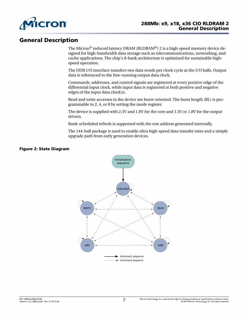
General DescriptionThe Micron® reduced latency DRAM (RLDRAM®) 2 is a high-speed memory device de-signed for high-bandwidth data storage such as telecommunications, networking, andcache applications. The chip’s 8-bank architecture is optimized for sustainable high-speed operation.
The DDR I/O interface transfers two data words per clock cycle at the I/O balls. Outputdata is referenced to the free-running output data clock.
Commands, addresses, and control signals are registered at every positive edge of thedifferential input clock, while input data is registered at both positive and negativeedges of the input data clock(s).
Read and write accesses to the device are burst-oriented. The burst length (BL) is pro-grammable to 2, 4, or 8 by setting the mode register.
The device is supplied with 2.5V and 1.8V for the core and 1.5V or 1.8V for the outputdrivers.
Bank-scheduled refresh is supported with the row address generated internally.
The 144-ball package is used to enable ultra high-speed data transfer rates and a simpleupgrade path from early generation devices.
PDF: 09005aef80a41b46rldram-2_cio_288mb.pdf - Rev. Q 10/15 EN 7 Micron Technology, Inc. reserves the right to change products or specifications without notice.
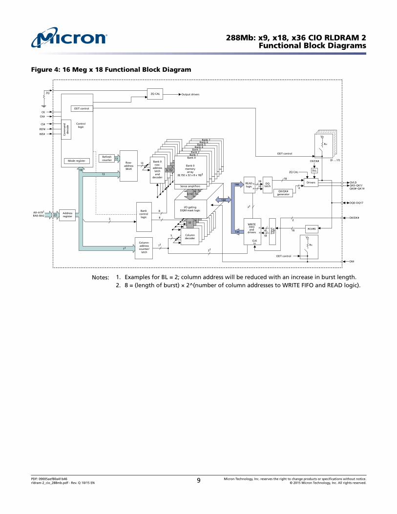
Notes: 1. Examples for BL = 2; column address will be reduced with an increase in burst length.2. 16 = (length of burst) × 2^(number of column addresses to WRITE FIFO and READ logic).
PDF: 09005aef80a41b46rldram-2_cio_288mb.pdf - Rev. Q 10/15 EN 8 Micron Technology, Inc. reserves the right to change products or specifications without notice.
Notes: 1. Examples for BL = 2; column address will be reduced with an increase in burst length.2. 8 = (length of burst) × 2^(number of column addresses to WRITE FIFO and READ logic).
PDF: 09005aef80a41b46rldram-2_cio_288mb.pdf - Rev. Q 10/15 EN 9 Micron Technology, Inc. reserves the right to change products or specifications without notice.
Notes: 1. Examples for BL = 2; column address will be reduced with an increase in burst length.2. 4 = (length of burst) × 2^(number of column addresses to WRITE FIFO and READ logic).
PDF: 09005aef80a41b46rldram-2_cio_288mb.pdf - Rev. Q 10/15 EN 10 Micron Technology, Inc. reserves the right to change products or specifications without notice.
Notes: 1. Reserved for future use. This signal is not connected.2. Reserved for future use. This signal is internally connected and has parasitic characteris-
tics of an address input signal.3. No function. This signal is internally connected and has parasitic characteristics of a clock
input signal. This may optionally be connected to GND.4. Do not use. This signal is internally connected and has parasitic characteristics of a I/O.
This may optionally be connected to GND. Note that if ODT is enabled on Rev. A die,these pins will be connected to VTT. The DNU pins are High-Z on Rev. B die when ODT isenabled.
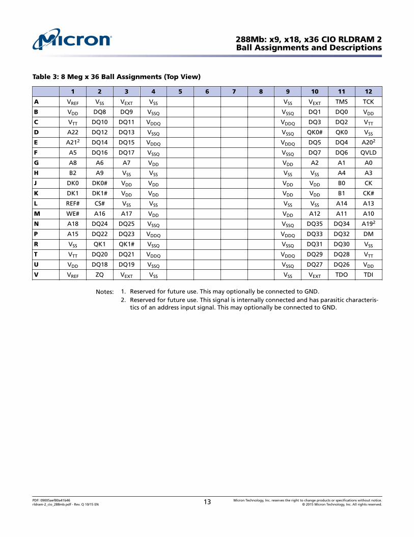
288Mb: x9, x18, x36 CIO RLDRAM 2Ball Assignments and Descriptions
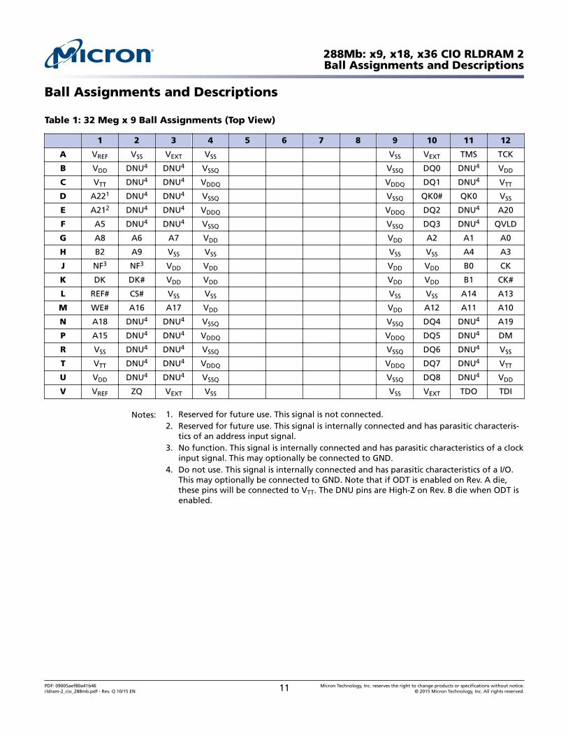
PDF: 09005aef80a41b46rldram-2_cio_288mb.pdf - Rev. Q 10/15 EN 11 Micron Technology, Inc. reserves the right to change products or specifications without notice.
Notes: 1. Reserved for future use. This may optionally be connected to GND.2. Reserved for future use. This signal is internally connected and has parasitic characteris-
tics of an address input signal. This may optionally be connected to GND.3. No function. This signal is internally connected and has parasitic characteristics of a clock
input signal. This may optionally be connected to GND.4. Do not use. This signal is internally connected and has parasitic characteristics of a I/O.
This may optionally be connected to GND. Note that if ODT is enabled on Rev. A die,these pins will be connected to VTT. The DNU pins are High-Z on Rev. B die when ODT isenabled.
288Mb: x9, x18, x36 CIO RLDRAM 2Ball Assignments and Descriptions
PDF: 09005aef80a41b46rldram-2_cio_288mb.pdf - Rev. Q 10/15 EN 12 Micron Technology, Inc. reserves the right to change products or specifications without notice.
Notes: 1. Reserved for future use. This may optionally be connected to GND.2. Reserved for future use. This signal is internally connected and has parasitic characteris-
tics of an address input signal. This may optionally be connected to GND.
288Mb: x9, x18, x36 CIO RLDRAM 2Ball Assignments and Descriptions
PDF: 09005aef80a41b46rldram-2_cio_288mb.pdf - Rev. Q 10/15 EN 13 Micron Technology, Inc. reserves the right to change products or specifications without notice.
A0–A20 Input Address inputs: A0–A20 define the row and column addresses for READ and WRITE operations.During a MODE REGISTER SET, the address inputs define the register settings. They are sampledat the rising edge of CK.
BA0–BA2 Input Bank address inputs: Select to which internal bank a command is being applied.
CK, CK# Input Input clock: CK and CK# are differential input clocks. Addresses and commands are latched onthe rising edge of CK. CK# is ideally 180 degrees out of phase with CK.
CS# Input Chip select: CS# enables the command decoder when LOW and disables it when HIGH. Whenthe command decoder is disabled, new commands are ignored, but internal operations continue.
DK, DK# Input Input data clock: DK and DK# are the differential input data clocks. All input data is referencedto both edges of DK. DK# is ideally 180 degrees out of phase with DK. For the x36 device, DQ0–DQ17 are referenced to DK0 and DK0# and DQ18–DQ35 are referenced to DK1 and DK1#. Forthe x9 and x18 devices, all DQs are referenced to DK and DK#. All DKx and DKx# pins must al-ways be supplied to the device.
DM Input Input data mask: The DM signal is the input mask signal for WRITE data. Input data is maskedwhen DM is sampled HIGH. DM is sampled on both edges of DK (DK1 for the x36 configuration).Tie signal to ground if not used.
TCK Input IEEE 1149.1 clock input: This ball must be tied to VSS if the JTAG function is not used.
TMS, TDI Input IEEE 1149.1 test inputs: These balls may be left as no connects if the JTAG function is not used.
WE#, REF# Input Command inputs: Sampled at the positive edge of CK, WE# and REF# define (together withCS#) the command to be executed.
DQ0–DQ35 I/O Data input: The DQ signals form the 36-bit data bus. During READ commands, the data is refer-enced to both edges of QKx. During WRITE commands, the data is sampled at both edges of DK.
ZQ Reference External impedance (25–60Ω): This signal is used to tune the device outputs to the system da-ta bus impedance. DQ output impedance is set to 0.2 × RQ, where RQ is a resistor from this signalto ground. Connecting ZQ to GND invokes the minimum impedance mode. Connecting ZQ toVDD invokes the maximum impedance mode. Refer to the Mode Register Definition in Nonmulti-plexed Address Mode figure to activate this function.
QKx, QKx# Output Output data clocks: QKx and QKx# are opposite polarity, output data clocks. They are free-run-ning, and during READs, are edge-aligned with data output from the RLDRAM. QKx# is ideally180 degrees out of phase with QKx. For the x36 device, QK0 and QK0# are aligned with DQ0–DQ17, and QK1 and QK1# are aligned with DQ18–DQ35. For the x18 device, QK0 and QK0# arealigned with DQ0–DQ8, while QK1 and QK1# are aligned with Q9–Q17. For the x9 device, all DQsare aligned with QK0 and QK0#.
QVLD Output Data valid: The QVLD pin indicates valid output data. QVLD is edge-aligned with QKx andQKx#.
TDO Output IEEE 1149.1 test output: JTAG output. This ball may be left as no connect if the JTAG functionis not used.
VDD Supply Power supply: Nominally, 1.8V. See the DC Electrical Characteristics and Operating Conditionstable for range.
VDDQ Supply DQ power supply: Nominally, 1.5V or 1.8V. Isolated on the device for improved noise immunity.See the DC Electrical Characteristics and Operating Conditions table for range.
VEXT Supply Power supply: Nominally, 2.5V. See the DC Electrical Characteristics and Operating Conditionstable for range.
288Mb: x9, x18, x36 CIO RLDRAM 2Ball Assignments and Descriptions
PDF: 09005aef80a41b46rldram-2_cio_288mb.pdf - Rev. Q 10/15 EN 14 Micron Technology, Inc. reserves the right to change products or specifications without notice.
VREF Supply Input reference voltage: Nominally VDDQ/2. Provides a reference voltage for the input buffers.
VSS Supply Ground.
VSSQ Supply DQ ground: Isolated on the device for improved noise immunity.
VTT Supply Power supply: Isolated termination supply. Nominally, VDDQ/2. See the DC Electrical Characteris-tics and Operating Conditions table for range.
A21 – Reserved for future use: This signal is internally connected and can be treated as an addressinput.
A22 – Reserved for future use: This signal is not connected and can be connected to ground.
DNU – Do not use: These balls may be connected to ground. Note that if ODT is enabled on Rev. A die,these pins will be connected to VTT. The DNU pins are High-Z on Rev. B die when ODT is enabled.
NF – No function: These balls can be connected to ground.
288Mb: x9, x18, x36 CIO RLDRAM 2Ball Assignments and Descriptions
PDF: 09005aef80a41b46rldram-2_cio_288mb.pdf - Rev. Q 10/15 EN 15 Micron Technology, Inc. reserves the right to change products or specifications without notice.
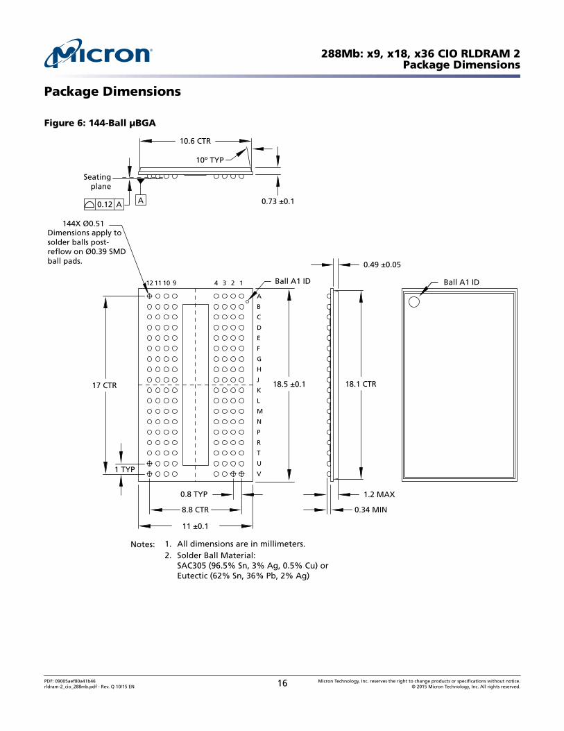
PDF: 09005aef80a41b46rldram-2_cio_288mb.pdf - Rev. Q 10/15 EN 16 Micron Technology, Inc. reserves the right to change products or specifications without notice.
PDF: 09005aef80a41b46rldram-2_cio_288mb.pdf - Rev. Q 10/15 EN 17 Micron Technology, Inc. reserves the right to change products or specifications without notice.
Table 5: IDD Operating Conditions and Maximum Limits – Rev. A
Notes appear after Rev. B tableDescription Condition Symbol -25 -33 -5 Units
Standby current tCK = idle; All banks idle; No inputs toggling ISB1 (VDD) x9/x18 48 48 48 mA
ISB1 (VDD) x36 48 48 48
ISB1 (VEXT) 26 26 26
Active standbycurrent
CS# = 1; No commands; Bank address incre-mented and half address/data change once ev-ery 4 clock cycles
ISB2 (VDD) x9/x18 288 233 189 mA
ISB2 (VDD) x36 288 233 189
ISB2 (VEXT) 26 26 26
Operational cur-rent
BL = 2; Sequential bank access; Bank transitionsonce every tRC; Half address transitions onceevery tRC; Read followed by write sequence;continuous data during WRITE commands
IDD1 (VDD) x9/x18 348 305 255 mA
IDD1 (VDD) x36 374 343 292
IDD1 (VEXT) 41 36 36
Operational cur-rent
BL = 4; Sequential bank access; Bank transitionsonce every tRC; Half address transitions onceevery tRC; Read followed by write sequence;Continuous data during WRITE commands
IDD2 (VDD) x9/x18 362 319 269 mA
IDD2 (VDD) x36 418 389 339
IDD2 (VEXT) 48 42 42
Operational cur-rent
BL = 8; Sequential bank access; Bank transitionsonce every tRC; half address transitions onceevery tRC; Read followed by write sequence;continuous data during WRITE commands
IDD3 (VDD) x9/x18 408 368 286 mA
IDD3 (VDD) x36 n/a n/a n/a
IDD3 (VEXT) 55 48 48
Burst refresh cur-rent
Eight-bank cyclic refresh; Continuous address/data; Command bus remains in refresh for alleight banks
IREF1 (VDD) x9/x18 785 615 430 mA
IREF1 (VDD) x36 785 615 430
IREF1 (VEXT) 133 111 105
Distributed refreshcurrent
Single-bank refresh; Sequential bank access;Half address transitions once every tRC, contin-uous data
IREF2 (VDD) x9/x18 325 267 221 mA
IREF2 (VDD) x36 326 281 227
IREF2 (VEXT) 48 42 42
Operating burstwrite current ex-ample
BL = 2; Cyclic bank access; Half of address bitschange every clock cycle; Continuous data;measurement is taken during continuousWRITE
IDD2W (VDD) x9/x18
970 819 597 mA
IDD2W (VDD) x36 990 914 676
IDD2W (VEXT) 100 90 69
Operating burstwrite current ex-ample
BL = 4; Cyclic bank access; Half of address bitschange every 2 clock cycles; Continuous data;Measurement is taken during continuousWRITE
IDD4W (VDD) x9/x18
779 609 439 mA
IDD4W (VDD) x36 882 790 567
IDD4W (VEXT) 88 77 63
Operating burstwrite current ex-ample
BL = 8; Cyclic bank access; Half of address bitschange every 4 clock cycles; continuous data;Measurement is taken during continuousWRITE
PDF: 09005aef80a41b46rldram-2_cio_288mb.pdf - Rev. Q 10/15 EN 18 Micron Technology, Inc. reserves the right to change products or specifications without notice.
PDF: 09005aef80a41b46rldram-2_cio_288mb.pdf - Rev. Q 10/15 EN 19 Micron Technology, Inc. reserves the right to change products or specifications without notice.
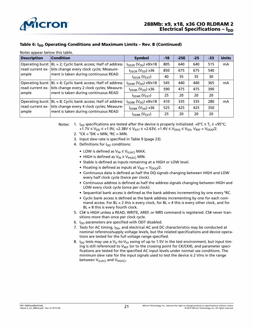
Table 6: IDD Operating Conditions and Maximum Limits – Rev. B
Notes appear below this table.Description Condition Symbol -18 -25E -25 -33 Units
Standby current tCK = idle; All banks idle; No inputs tog-gling
ISB1 (VDD) x9/x18 55 55 55 55 mA
ISB1 (VDD) x36 55 55 55 55
ISB1 (VEXT) 5 5 5 5
Active standbycurrent
CS# = 1; No commands; Bank address in-cremented and half address/data changeonce every 4 clock cycles
ISB2 (VDD) x9/x18 250 215 215 190 mA
ISB2 (VDD) x36 250 215 215 190
ISB2 (VEXT) 5 5 5 5
Operationalcurrent
BL = 2; Sequential bank access; Banktransitions once every tRC; Half addresstransitions once every tRC; Read followedby write sequence; continuous data dur-ing WRITE commands
IDD1 (VDD) x9/x18 310 285 260 225 mA
IDD1 (VDD) x36 320 295 270 230
IDD1 (VEXT) 10 10 10 10
Operationalcurrent
BL = 4; Sequential bank access; Banktransitions once every tRC; Half addresstransitions once every tRC; Read followedby write sequence; Continuous data dur-ing WRITE commands
IDD2 (VDD) x9/x18 315 290 260 220 mA
IDD2 (VDD) x36 330 305 275 230
IDD2 (VEXT) 10 10 10 10
Operationalcurrent
BL = 8; Sequential bank access; Banktransitions once every tRC; half addresstransitions once every tRC; Read followedby write sequence; continuous data dur-ing WRITE commands
IDD3 (VDD) x9/x18 330 305 275 230 mA
IDD3 (VDD) x36 390 365 320 265
IDD3 (VEXT) 15 15 15 15
Burst refreshcurrent
Eight-bank cyclic refresh; Continuous ad-dress/data; Command bus remains in re-fresh for all eight banks
IREF1 (VDD) x9/x18 660 540 530 430 mA
IREF1 (VDD) x36 670 545 535 435
IREF1 (VEXT) 45 30 30 25
Distributed re-fresh current
Single-bank refresh; Sequential bank ac-cess; Half address transitions once everytRC, continuous data
IREF2 (VDD) x9/x18 295 265 250 215 mA
IREF2 (VDD) x36 295 265 250 215
IREF2 (VEXT) 10 10 10 10
Operating burstwrite currentexample
BL = 2; Cyclic bank access; Half of addressbits change every clock cycle; Continuousdata; measurement is taken during con-tinuous WRITE
IDD2W (VDD) x9/x18
830 655 655 530 mA
IDD2W (VDD) x36 885 700 700 565
IDD2W (VEXT) 40 35 35 30
Operating burstwrite currentexample
BL = 4; Cyclic bank access; Half of addressbits change every 2 clock cycles; Continu-ous data; Measurement is taken duringcontinuous WRITE
IDD4W (VDD) x9/x18
580 465 465 385 mA
IDD4W (VDD) x36 635 510 510 420
IDD4W (VEXT) 25 20 20 20
Operating burstwrite currentexample
BL = 8; Cyclic bank access; Half of addressbits change every 4 clock cycles; continu-ous data; Measurement is taken duringcontinuous WRITE
PDF: 09005aef80a41b46rldram-2_cio_288mb.pdf - Rev. Q 10/15 EN 20 Micron Technology, Inc. reserves the right to change products or specifications without notice.
Table 6: IDD Operating Conditions and Maximum Limits – Rev. B (Continued)
Notes appear below this table.Description Condition Symbol -18 -25E -25 -33 Units
Operating burstread current ex-ample
BL = 2; Cyclic bank access; Half of addressbits change every clock cycle; Measure-ment is taken during continuous READ
IDD2R (VDD) x9/x18 805 640 640 515 mA
IDD2R (VDD) x36 850 675 675 540
IDD2R (VEXT) 40 35 35 30
Operating burstread current ex-ample
BL = 4; Cyclic bank access; Half of addressbits change every 2 clock cycles; Measure-ment is taken during continuous READ
IDD4R (VDD) x9/x18 545 440 440 365 mA
IDD4R (VDD) x36 590 475 475 390
IDD4R (VEXT) 25 20 20 20
Operating burstread current ex-ample
BL = 8; Cyclic bank access; Half of addressbits change every 4 clock cycles; Measure-ment is taken during continuous READ
IDD8R (VDD) x9/x18 410 335 335 280 mA
IDD8R (VDD) x36 525 425 425 350
IDD8R (VEXT) 25 20 20 20
Notes: 1. IDD specifications are tested after the device is properly initialized. +0°C ≤ Tc ≤ +95°C;+1.7V ≤ VDD ≤ +1.9V, +2.38V ≤ VEXT ≤ +2.63V, +1.4V ≤ VDDQ ≤ VDD, VREF = VDDQ/2.
2. tCK = tDK = MIN, tRC = MIN.3. Input slew rate is specified in Table 9 (page 23).4. Definitions for IDD conditions:
• LOW is defined as VIN ≤ VIL(AC) MAX.• HIGH is defined as VIN ≥ VIH(AC) MIN.• Stable is defined as inputs remaining at a HIGH or LOW level.• Floating is defined as inputs at VREF = VDDQ/2.• Continuous data is defined as half the DQ signals changing between HIGH and LOW
every half clock cycle (twice per clock).• Continuous address is defined as half the address signals changing between HIGH and
LOW every clock cycle (once per clock).• Sequential bank access is defined as the bank address incrementing by one every tRC.• Cyclic bank access is defined as the bank address incrementing by one for each com-
mand access. For BL = 2 this is every clock, for BL = 4 this is every other clock, and for BL = 8 this is every fourth clock.
5. CS# is HIGH unless a READ, WRITE, AREF, or MRS command is registered. CS# never tran-sitions more than once per clock cycle.
6. IDD parameters are specified with ODT disabled.7. Tests for AC timing, IDD, and electrical AC and DC characteristics may be conducted at
nominal reference/supply voltage levels, but the related specifications and device opera-tions are tested for the full voltage range specified.
8. IDD tests may use a VIL-to-VIH swing of up to 1.5V in the test environment, but input tim-ing is still referenced to VREF (or to the crossing point for CK/CK#), and parameter speci-fications are tested for the specified AC input levels under normal use conditions. Theminimum slew rate for the input signals used to test the device is 2 V/ns in the rangebetween VIL(AC) and VIH(AC).
PDF: 09005aef80a41b46rldram-2_cio_288mb.pdf - Rev. Q 10/15 EN 21 Micron Technology, Inc. reserves the right to change products or specifications without notice.
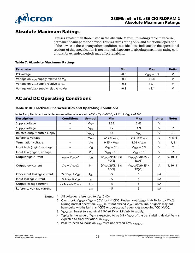
Absolute Maximum RatingsStresses greater than those listed in the Absolute Maximum Ratings table may causepermanent damage to the device. This is a stress rating only, and functional operationof the device at these or any other conditions outside those indicated in the operationalsections of this specification is not implied. Exposure to absolute maximum rating con-ditions for extended periods may affect reliability.
Table 7: Absolute Maximum Ratings
Parameter Min Max Units
I/O voltage –0.3 VDDQ + 0.3 V
Voltage on VEXT supply relative to VSS –0.3 +2.8 V
Voltage on VDD supply relative to VSS –0.3 +2.1 V
Voltage on VDDQ supply relative to VSS –0.3 +2.1 V
AC and DC Operating Conditions
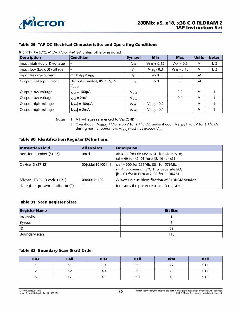
Table 8: DC Electrical Characteristics and Operating Conditions
Note 1 applies to entire table; unless otherwise noted: +0°C ≤ TC ≤ +95°C; +1.7V ≤ VDD ≤ +1.9VDescription Conditions Symbol Min Max Units Notes
Notes: 1. All voltages referenced to VSS (GND).2. Overshoot: VIH(AC) ≤ VDD + 0.7V for t ≤ tCK/2. Undershoot: VIL(AC) ≥ –0.5V for t ≤ tCK/2.
During normal operation, VDDQ must not exceed VDD. Control input signals may nothave pulse widths less than tCK/2 or operate at frequencies exceeding tCK (MAX).
3. VDDQ can be set to a nominal 1.5V ±0.1V or 1.8V ±0.1V supply.4. Typically the value of VREF is expected to be 0.5 × VDDQ of the transmitting device. VREF is
expected to track variations in VDDQ.5. Peak-to-peak AC noise on VREF must not exceed ±2% VREF(DC).
288Mb: x9, x18, x36 CIO RLDRAM 2Absolute Maximum Ratings
PDF: 09005aef80a41b46rldram-2_cio_288mb.pdf - Rev. Q 10/15 EN 22 Micron Technology, Inc. reserves the right to change products or specifications without notice.
6. VREF is expected to equal VDDQ/2 of the transmitting device and to track variations in theDC level of the same. Peak-to-peak noise (non-common mode) on VREF may not exceed±2% of the DC value. Thus, from VDDQ/2, VREF is allowed ±2% VDDQ/2 for DC error andan additional ±2% VDDQ/2 for AC noise. This measurement is to be taken at the nearestVREF bypass capacitor.
7. VTT is expected to be set equal to VREF and must track variations in the DC level of VREF.8. On-die termination may be selected using mode register bit 9 (see Mode Register Defini-
tion in Nonmultiplexed Address Mode). A resistance RTT from each data input signal tothe nearest VTT can be enabled. RTT = 125–185Ω at 95°C TC.
9. IOH and IOL are defined as absolute values and are measured at VDDQ/2. IOH flows fromthe device, IOL flows into the device.
10. If MRS bit A8 is 0, use RQ = 250Ω in the equation in lieu of presence of an external im-pedance matched resistor.
11. For VOL and VOH, refer to the device HSPICE or IBIS driver models.
Table 9: Input AC Logic Levels
Notes 1–3 apply to entire table; unless otherwise noted: +0°C ≤ TC ≤ +95°C; +1.7V ≤ VDD ≤ +1.9VDescription Symbol Min Max Units
Input high (logic 1) voltage VIH VREF + 0.2 – V
Input low (logic 0) voltage VIL – VREF - 0.2 V
Notes: 1. All voltages referenced to VSS (GND).2. The AC and DC input level specifications are as defined in the HSTL standard (that is, the
receiver will effectively switch as a result of the signal crossing the AC input level andwill remain in that state as long as the signal does not ring back above [below] the DCinput LOW [HIGH] level).
3. The minimum slew rate for the input signals used to test the device is 2 V/ns in therange between VIL(AC) and VIH(AC) (see Minimum Slew Rate figure below).
Figure 8: Minimum Slew Rate
VIH(AC) MIN
VIL(AC) MAX
Rise time: 2 V/ns
Fall time:2 V/ns
VDDQ
GND
VSWING
288Mb: x9, x18, x36 CIO RLDRAM 2AC and DC Operating Conditions
PDF: 09005aef80a41b46rldram-2_cio_288mb.pdf - Rev. Q 10/15 EN 23 Micron Technology, Inc. reserves the right to change products or specifications without notice.
Notes 1–4 apply to entire table; unless otherwise noted: +0°C ≤ TC ≤ +95°C; +1.7V ≤ VDD ≤ +1.9VParameter/Condition Symbol Min Max Units Notes
Clock input voltage level: CK and CK# VIN(DC) –0.3 VDDQ + 0.3 V
Clock input differential voltage: CK and CK# VID(DC) 0.2 VDDQ + 0.6 V 5
Clock input differential voltage: CK and CK# VID(AC) 0.4 VDDQ + 0.6 V 5
Clock input crossing point voltage: CK andCK#
VIX(AC) VDDQ/2 - 0.15 VDDQ/2 + 0.15 V 6
Notes: 1. DKx and DKx# have the same requirements as CK and CK#.2. All voltages referenced to VSS (GND).3. The CK/CK# input reference level (for timing referenced to CK/CK#) is the point at which
CK and CK# cross. The input reference level for signals other than CK/CK# is VREF.4. CK and CK# input slew rate must be ≥2 V/ns (≥4 V/ns if measured differentially).5. VID is the magnitude of the difference between the input level on CK and the input lev-
el on CK#.6. The value of VIX is expected to equal VDDQ/2 of the transmitting device and must track
variations in the DC level of the same.
Figure 9: Clock Input
CK
CK#
VIN(DC) MAX
1
Maximum clock level
Minimum clock levelVIN(DC) MIN
VDDQ/2
VDDQ/2 + 0.15
VDDQ/2A - 0.15 X
XVID(AC)
3VID(DC)
2VIX(AC) MAX
VIX(AC) MIN
Notes: 1. CK and CK# must cross within this region.2. CK and CK# must meet at least VID(DC) MIN when static and centered around VDDQ/2.3. Minimum peak-to-peak swing.4. It is a violation to tristate CK and CK# after the part is initialized.
288Mb: x9, x18, x36 CIO RLDRAM 2AC and DC Operating Conditions
PDF: 09005aef80a41b46rldram-2_cio_288mb.pdf - Rev. Q 10/15 EN 24 Micron Technology, Inc. reserves the right to change products or specifications without notice.
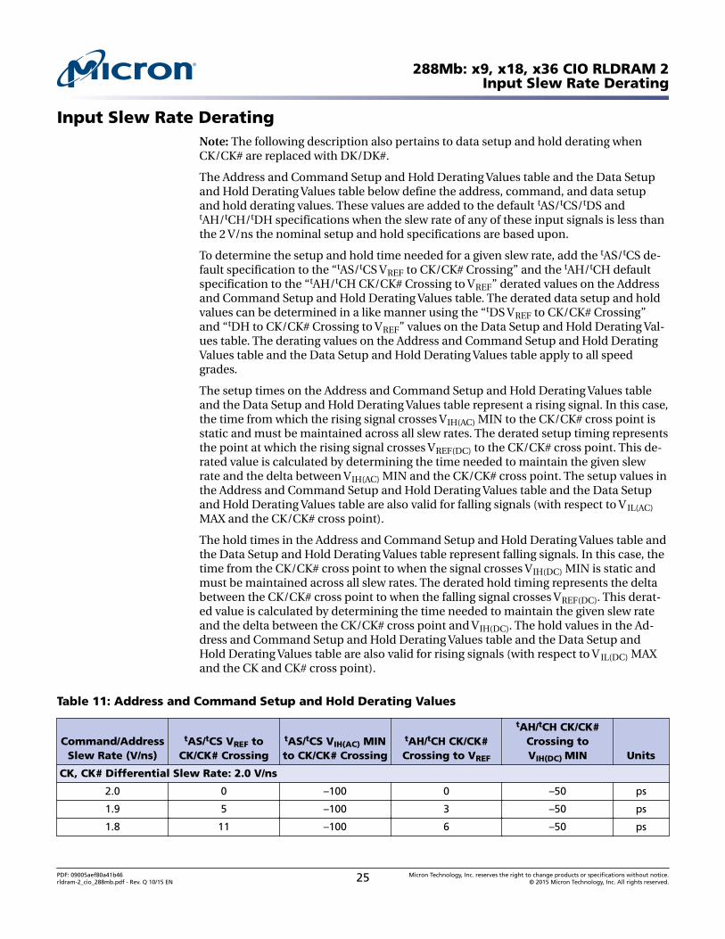
Input Slew Rate DeratingNote: The following description also pertains to data setup and hold derating whenCK/CK# are replaced with DK/DK#.
The Address and Command Setup and Hold Derating Values table and the Data Setupand Hold Derating Values table below define the address, command, and data setupand hold derating values. These values are added to the default tAS/tCS/tDS andtAH/tCH/tDH specifications when the slew rate of any of these input signals is less thanthe 2 V/ns the nominal setup and hold specifications are based upon.
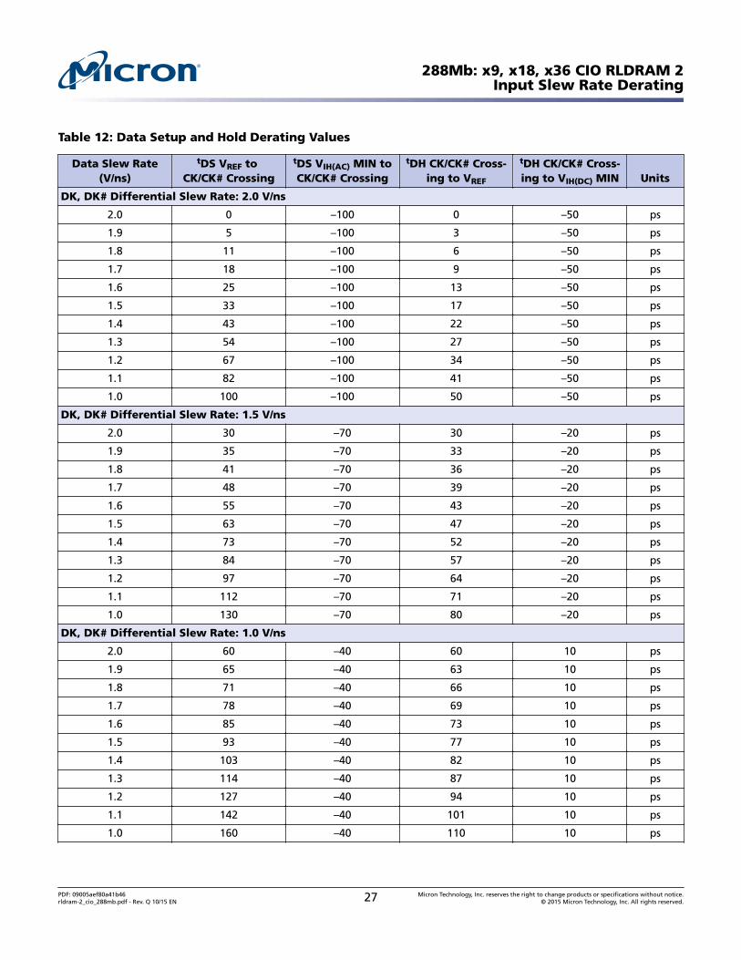
To determine the setup and hold time needed for a given slew rate, add the tAS/tCS de-fault specification to the “tAS/tCS VREF to CK/CK# Crossing” and the tAH/tCH defaultspecification to the “tAH/tCH CK/CK# Crossing to VREF” derated values on the Addressand Command Setup and Hold Derating Values table. The derated data setup and holdvalues can be determined in a like manner using the “tDS VREF to CK/CK# Crossing”and “tDH to CK/CK# Crossing to VREF” values on the Data Setup and Hold Derating Val-ues table. The derating values on the Address and Command Setup and Hold DeratingValues table and the Data Setup and Hold Derating Values table apply to all speedgrades.
The setup times on the Address and Command Setup and Hold Derating Values tableand the Data Setup and Hold Derating Values table represent a rising signal. In this case,the time from which the rising signal crosses VIH(AC) MIN to the CK/CK# cross point isstatic and must be maintained across all slew rates. The derated setup timing representsthe point at which the rising signal crosses VREF(DC) to the CK/CK# cross point. This de-rated value is calculated by determining the time needed to maintain the given slewrate and the delta between VIH(AC) MIN and the CK/CK# cross point. The setup values inthe Address and Command Setup and Hold Derating Values table and the Data Setupand Hold Derating Values table are also valid for falling signals (with respect to V IL(AC)MAX and the CK/CK# cross point).
The hold times in the Address and Command Setup and Hold Derating Values table andthe Data Setup and Hold Derating Values table represent falling signals. In this case, thetime from the CK/CK# cross point to when the signal crosses VIH(DC) MIN is static andmust be maintained across all slew rates. The derated hold timing represents the deltabetween the CK/CK# cross point to when the falling signal crosses VREF(DC). This derat-ed value is calculated by determining the time needed to maintain the given slew rateand the delta between the CK/CK# cross point and VIH(DC). The hold values in the Ad-dress and Command Setup and Hold Derating Values table and the Data Setup andHold Derating Values table are also valid for rising signals (with respect to V IL(DC) MAXand the CK and CK# cross point).
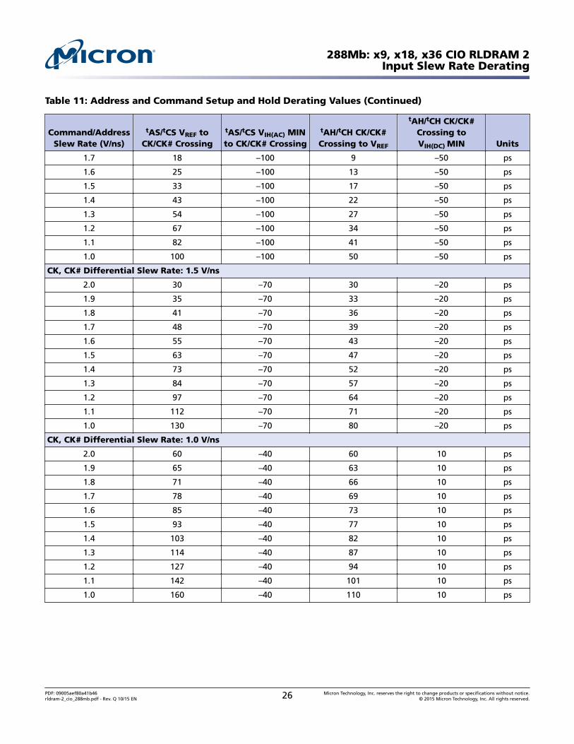
Table 11: Address and Command Setup and Hold Derating Values
PDF: 09005aef80a41b46rldram-2_cio_288mb.pdf - Rev. Q 10/15 EN 25 Micron Technology, Inc. reserves the right to change products or specifications without notice.
PDF: 09005aef80a41b46rldram-2_cio_288mb.pdf - Rev. Q 10/15 EN 26 Micron Technology, Inc. reserves the right to change products or specifications without notice.
PDF: 09005aef80a41b46rldram-2_cio_288mb.pdf - Rev. Q 10/15 EN 27 Micron Technology, Inc. reserves the right to change products or specifications without notice.
PDF: 09005aef80a41b46rldram-2_cio_288mb.pdf - Rev. Q 10/15 EN 28 Micron Technology, Inc. reserves the right to change products or specifications without notice.
PDF: 09005aef80a41b46rldram-2_cio_288mb.pdf - Rev. Q 10/15 EN 29 Micron Technology, Inc. reserves the right to change products or specifications without notice.
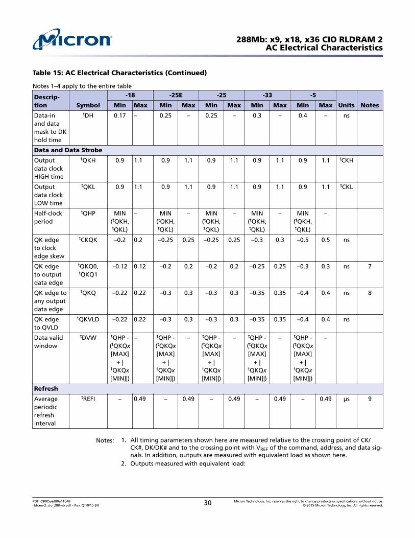
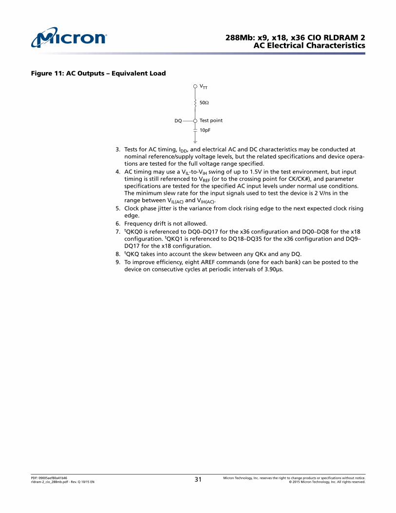
Notes: 1. All timing parameters shown here are measured relative to the crossing point of CK/CK#, DK/DK# and to the crossing point with VREF of the command, address, and data sig-nals. In addition, outputs are measured with equivalent load as shown here.
PDF: 09005aef80a41b46rldram-2_cio_288mb.pdf - Rev. Q 10/15 EN 30 Micron Technology, Inc. reserves the right to change products or specifications without notice.
3. Tests for AC timing, IDD, and electrical AC and DC characteristics may be conducted atnominal reference/supply voltage levels, but the related specifications and device opera-tions are tested for the full voltage range specified.
4. AC timing may use a VIL-to-VIH swing of up to 1.5V in the test environment, but inputtiming is still referenced to VREF (or to the crossing point for CK/CK#), and parameterspecifications are tested for the specified AC input levels under normal use conditions.The minimum slew rate for the input signals used to test the device is 2 V/ns in therange between VIL(AC) and VIH(AC).
5. Clock phase jitter is the variance from clock rising edge to the next expected clock risingedge.
6. Frequency drift is not allowed.7. tQKQ0 is referenced to DQ0–DQ17 for the x36 configuration and DQ0–DQ8 for the x18
configuration. tQKQ1 is referenced to DQ18–DQ35 for the x36 configuration and DQ9–DQ17 for the x18 configuration.
8. tQKQ takes into account the skew between any QKx and any DQ.9. To improve efficiency, eight AREF commands (one for each bank) can be posted to the
device on consecutive cycles at periodic intervals of 3.90µs.
PDF: 09005aef80a41b46rldram-2_cio_288mb.pdf - Rev. Q 10/15 EN 31 Micron Technology, Inc. reserves the right to change products or specifications without notice.
Temperature and Thermal ImpedanceIt is imperative that the temperature specifications shown in the Temperature Limits ta-ble are maintained to ensure that the junction temperature is in the proper operatingrange to meet data sheet specifications. An important step in maintaining the properjunction temperature is using the device’s thermal impedances correctly. The thermalimpedances are listed for the available packages.
Using thermal impedances incorrectly can produce significant errors. Read Micron'sTN-00-08: Thermal Applications technical note prior to using the thermal impedanceslisted in the Temperature Limits table. For designs that are expected to last several yearsand require the flexibility to use several DRAM die shrinks, consider using final targettheta values (rather than existing values) to account for increased thermal impedancesfrom the die size reduction.
The safe junction temperature range can be maintained when the TC specification isnot exceeded. In applications where the device’s ambient temperature is too high, theuse of forced air and/or heat sinks may be required in order to satisfy the case tempera-ture specifications.
Table 16: Temperature Limits
Parameter Symbol Min Max Units Notes
Storage temperature TSTG –55 +150 °C 1
Reliability junction temperature Commercial TJ – +110 °C 2
Industrial – +110 °C 2
Operating junction temperature Commercial TJ 0 +100 °C 3
Industrial –40 +100 °C 3
Operating case temperature Commercial TC 0 +95 °C 4, 5
Industrial –40 +95 °C 4, 5, 6
Notes: 1. Max storage case temperature, TSTG , is measured in the center of the package, as shownin the Example Temperature Test Point Location figure. This case temperature limit canbe exceeded briefly during package reflow, as noted in Micron's TN-00-15: Recommen-ded Soldering Parameters technical note.
2. Temperatures greater than 110°C may cause permanent damage to the device. This is astress rating only and functional operation of the device at or above this is not implied.Exposure to absolute maximum rating conditions for extended periods may affect thereliability of the part.
3. Junction temperature depends upon package type, cycle time, loading, ambient temper-ature, and airflow.
4. MAX operating case temperature; TC is measured in the center of the package, as shownin the Example Temperature Test Point Location figure.
5. Device functionality is not guaranteed if the device exceeds maximum TC during opera-tion.
6. Both temperature specifications must be satisfied.
288Mb: x9, x18, x36 CIO RLDRAM 2Temperature and Thermal Impedance
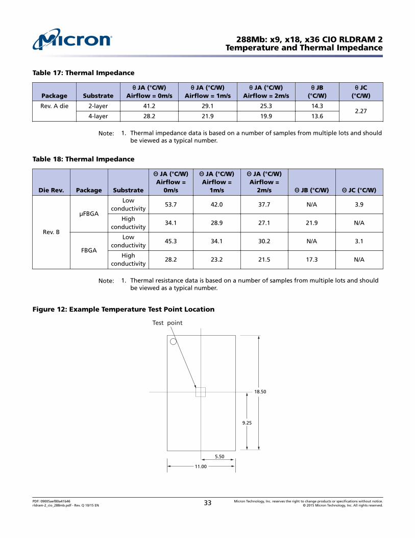
PDF: 09005aef80a41b46rldram-2_cio_288mb.pdf - Rev. Q 10/15 EN 32 Micron Technology, Inc. reserves the right to change products or specifications without notice.
Note: 1. Thermal impedance data is based on a number of samples from multiple lots and shouldbe viewed as a typical number.
Table 18: Thermal Impedance
Die Rev. Package Substrate
Θ JA (°C/W)Airflow =
0m/s
Θ JA (°C/W)Airflow =
1m/s
Θ JA (°C/W)Airflow =
2m/s Θ JB (°C/W) Θ JC (°C/W)
Rev. B
µFBGA
Lowconductivity
53.7 42.0 37.7 N/A 3.9
Highconductivity
34.1 28.9 27.1 21.9 N/A
FBGA
Lowconductivity
45.3 34.1 30.2 N/A 3.1
Highconductivity
28.2 23.2 21.5 17.3 N/A
Note: 1. Thermal resistance data is based on a number of samples from multiple lots and shouldbe viewed as a typical number.
Figure 12: Example Temperature Test Point Location
11.00
5.50
18.50
9.25
Test point
288Mb: x9, x18, x36 CIO RLDRAM 2Temperature and Thermal Impedance
PDF: 09005aef80a41b46rldram-2_cio_288mb.pdf - Rev. Q 10/15 EN 33 Micron Technology, Inc. reserves the right to change products or specifications without notice.
CommandsAll input states or sequences not shown are illegal or reserved. All command and ad-dress inputs must meet setup and hold times around the rising edge of CK.
Table 19: Description of Commands
Command Description Notes
DSEL/NOP The NOP command is used to perform a no operation to the device, which essentially deselectsthe chip. Use the NOP command to prevent unwanted commands from being registered duringidle or wait states. Operations already in progress are not affected. Output values depend oncommand history.
1
MRS The mode register is set via the address inputs A0–A17. See the Mode Register Definition inNonmultiplexed Address Mode figure for further information. The MRS command can only beissued when all banks are idle and no other operation is in progress.
READ The READ command is used to initiate a burst read access to a bank. The value on the BA0–BA2inputs selects the bank, and the address provided on inputs A0–An selects the data locationwithin the bank.
2
WRITE The WRITE command is used to initiate a burst write access to a bank. The value on the BA0–BA2 inputs selects the bank, and the address provided on inputs A0–An selects the data locationwithin the bank. Input data appearing on the DQ is written to the memory array subject to theDM input logic level appearing coincident with the data. If the DM signal is registered LOW, thecorresponding data will be written to memory. If the DM signal is registered HIGH, the corre-sponding data inputs will be ignored (that is, this part of the data word will not be written).
2
AUTO RE-FRESH (AREF)
The AREF command is used during normal device operation to refresh the memory content of abank. The command is nonpersistent, so it must be issued each time a refresh is required. Thevalue on the BA0–BA2 inputs selects the bank. The refresh address is generated by an internalrefresh controller, effectively making each address bit a “Don’t Care” during the AREF com-mand. See the AUTO REFRESH (AREF) section for more details.
Notes: 1. When the chip is deselected, internal NOP commands are generated and no commandsare accepted.
2. n = 20.
Table 20: Command Table
Operation Code CS# WE# REF# A0–An2 BA0–BA2 Notes
DEVICE DESELECT/NO OPERATION DSEL/NOP H X X X X
MRS MRS L L L OPCODE X 3
READ READ L H H A BA 4
WRITE WRITE L L H A BA 4
AUTO REFRESH AREF L H L X BA
Notes: 1. Applies to entire table: X = “Don’t Care;” H = logic HIGH; L = logic LOW; A = valid ad-dress; BA = valid bank address; n = 20.
2. Only A0–A17 are used for the MRS command.3. Address width varies with burst length; see the Address Widths at Different Burst
Lengths table.
288Mb: x9, x18, x36 CIO RLDRAM 2Commands
PDF: 09005aef80a41b46rldram-2_cio_288mb.pdf - Rev. Q 10/15 EN 34 Micron Technology, Inc. reserves the right to change products or specifications without notice.
MODE REGISTER SET (MRS) CommandThe mode register set stores the data for controlling the operating modes of the memo-ry. It programs the configuration, burst length, test mode, and I/O options. During anMRS command, the address inputs A0–A17 are sampled and stored in the mode regis-ter. After issuing a valid MRS command, tMRSC must be met before any command canbe issued to the device. This statement does not apply to the consecutive MRS com-mands needed for internal logic reset during the initialization routine. The MRS com-mand can only be issued when all banks are idle and no other operation is in progress.
Note: The data written by the prior burst length is not guaranteed to be accurate whenthe burst length of the device is changed.
PDF: 09005aef80a41b46rldram-2_cio_288mb.pdf - Rev. Q 10/15 EN 35 Micron Technology, Inc. reserves the right to change products or specifications without notice.
Figure 14: Mode Register Definition in Nonmultiplexed Address Mode
ConfigBLAMReserved1
A9A10 A7 A6 A5 A4 A3A8 A2 A1 A0
Mode Register (Mx)
Address Bus
9 7 6 5 4 38 2 1 0
A17
17–10
Configuration
13 (default)
13
2
3
43
5
Reserved
Reserved
M0
0
1
0
1
0
1
0
1
M1
0
0
1
1
0
0
1
1
M2
0
0
0
0
1
1
1
1
M5
0
1
Address MUX
Nonmultiplexed (default)
Multiplexed
M8
0
1
Drive Impedance
Internal 50Ω5 (default)
External (ZQ)
M9
0
1
On-Die Termination
Off (default)
On
DLL NA2ODT
M3
0
1
0
1
Burst Length
2 (default)
4
8
Reserved
M4
0
0
1
1
IM
. . .
M7
0
1
DLL Reset
DLL reset4 (default)
DLL enabled
Notes: 1. A10–A17 must be set to zero; A18–An = “Don’t Care.”2. A6 not used in MRS.3. BL = 8 is not available.4. DLL RESET turns the DLL off.5. ±30% temperature variation.
PDF: 09005aef80a41b46rldram-2_cio_288mb.pdf - Rev. Q 10/15 EN 36 Micron Technology, Inc. reserves the right to change products or specifications without notice.
The table here shows the different configurations that can be programmed into themode register. The WRITE latency is equal to the READ latency plus one in each config-uration in order to maximize data bus utilization. Bits M0, M1, and M2 are used to se-lect the configuration during the MRS command.
Table 21: Cycle Time and READ/WRITE Latency Configuration Table
Valid frequency range 266–175 400–175 533–175 200–175 333–175 MHz
Notes: 1. tRC < 20ns in any configuration only available with -25E and -18 speed grades.2. BL = 8 is not available.3. The minimum tRC is typically 3 cycles, except in the case of a WRITE followed by a READ
to the same bank. In this instance the minimum tRC is 4 cycles.
Burst Length (BL)
Burst length is defined by mode register bits M3 and M4. Device read and write accessesare burst-oriented, with burst length programmable to 2, 4, or 8. Shown here are the dif-ferent burst lengths with respect to a READ command. Changes to burst length affectthe width of the address bus (see the Address Widths at Different Burst Lengths table).
Note: When the device burst length is changed, data written by a prior burst length isnot guaranteed as accurate.
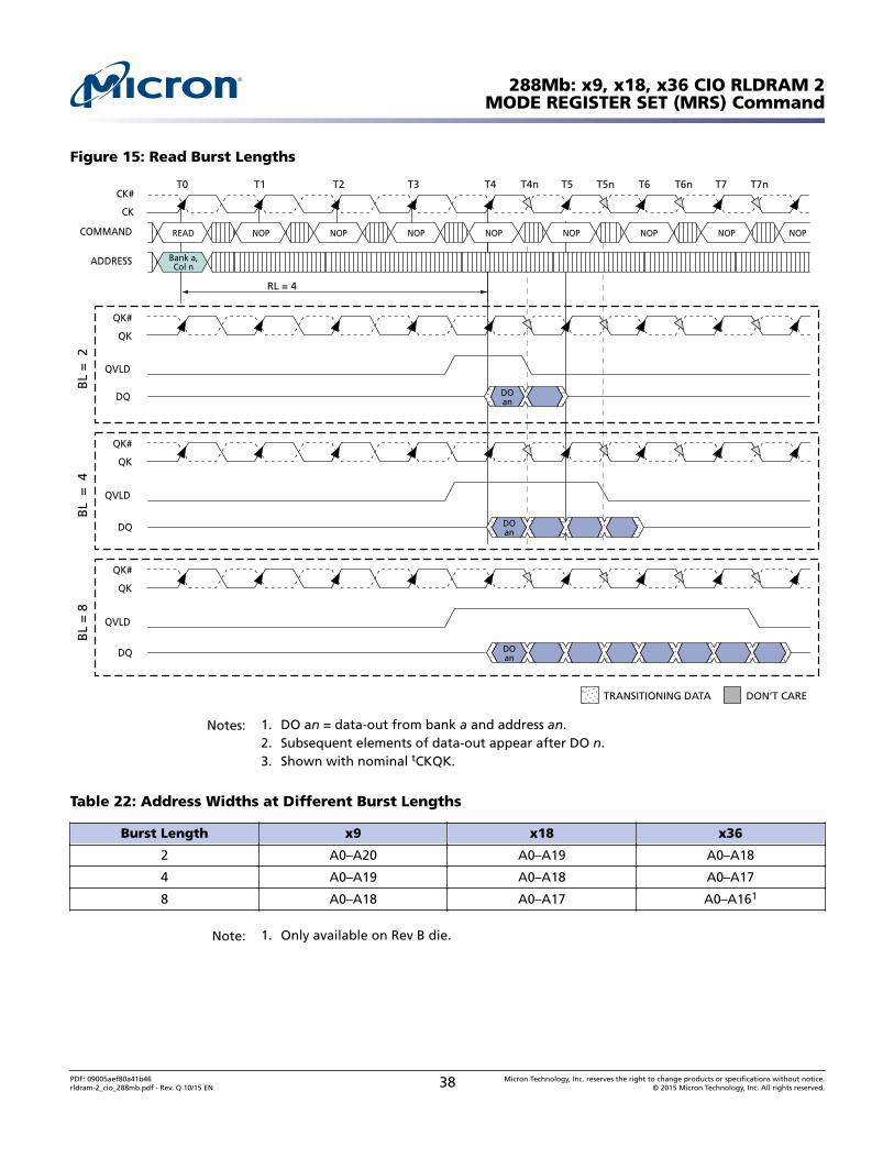
PDF: 09005aef80a41b46rldram-2_cio_288mb.pdf - Rev. Q 10/15 EN 37 Micron Technology, Inc. reserves the right to change products or specifications without notice.
PDF: 09005aef80a41b46rldram-2_cio_288mb.pdf - Rev. Q 10/15 EN 38 Micron Technology, Inc. reserves the right to change products or specifications without notice.
The multiplexed address option is available by setting mode register bit M5 to 1. Oncethis bit is set, the READ, WRITE, and MRS commands follow the format described in theCommand Description in Multiplexed Address Mode figure. Further information on op-eration with multiplexed addresses can be seen in the Multiplexed Address Mode sec-tion.
Although the device has the ability to operate with an SRAM interface by accepting theentire address in one clock, an option in the mode register can be set so that it functionswith multiplexed addresses, similar to a traditional DRAM.
In multiplexed address mode, the address can be provided to the device in two partsthat are latched into the memory with two consecutive rising clock edges. This providesthe advantage of only needing a maximum of 11 address balls to control the device, re-ducing the number of signals on the controller side. The data bus efficiency in continu-ous burst mode is only affected when using the BL = 2 setting because the device re-quires two clocks to read and write the data.
The bank addresses are delivered to the device at the same time as the WRITE andREAD command and the first address part, Ax. The Address Mapping in MultiplexedAddress Mode table shows the addresses needed for both the first and second risingclock edges (Ax and Ay, respectively).
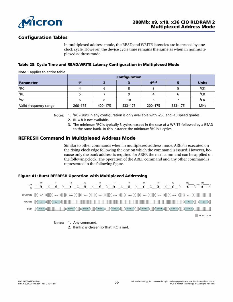
The AREF command does not require an address on the second rising clock edge, as on-ly the bank address is needed during this command. Because of this, AREF commandsmay be issued on consecutive clocks.
DLL RESET
DLL reset is selected with bit M7 of the mode register. The default setting for this optionis LOW, whereby the DLL is disabled.
Once M7 is set HIGH, 1024 cycles (5µs at 200 MHz) are needed before a READ com-mand can be issued. This time enables the internal clock to be synchronized with theexternal clock.
Failing to wait for synchronization to occur may result in a violation of the tCKQK pa-rameter.
A reset of the DLL is necessary if tCK or VDD is changed after the DLL has already beenenabled. To reset the DLL, an MRS command must be issued where M7 is set LOW. Afterwaiting tMRSC, a subsequent MRS command should be issued whereby M7 goes HIGH.1024 clock cycles are then needed before a READ command is issued.
Drive Impedance Matching
The device is equipped with programmable impedance output buffers. This option isselected by setting bit M8 HIGH during the MRS command. The purpose of the pro-grammable impedance output buffers is to enable the user to match the driver impe-dance to the system. To adjust the impedance, an external precision resistor (RQ) isconnected between the ZQ ball and VSS. The value of the resistor must be five times thedesired impedance. For example, a 300Ω resistor is required for an output impedance of60Ω. The range of RQ is 125–300Ω, which guarantees output impedance in the range of25–60Ω (within 15%).
PDF: 09005aef80a41b46rldram-2_cio_288mb.pdf - Rev. Q 10/15 EN 39 Micron Technology, Inc. reserves the right to change products or specifications without notice.
Output impedance updates may be required because over time variations may occur insupply voltage and temperature. When the external drive impedance is enabled in theMRS, the device will periodically sample the value of RQ. An impedance update is trans-parent to the system and does not affect device operation. All data sheet timing andcurrent specifications are met during an update.
When bit M8 is set LOW during the MRS command, the device provides an internal im-pedance at the output buffer of 50Ω (±30% with temperature variation). This impe-dance is also periodically sampled and adjusted to compensate for variation in supplyvoltage and temperature.
On-Die Termination (ODT)
ODT is enabled by setting M9 to a value of 1 during an MRS command. With ODT on,the DQ and DM are terminated to VTT with a resistance RTT. The command, address,QVLD, and clock signals are not terminated.
The ODT function is dynamically switched off when DQ begins to drive after a READcommand is issued. Similarly, ODT is designed to switch on at DQ after the device hasissued the last piece of data. The DM pin will always be terminated.
Table 23: On-Die Termination DC Parameters
Description Symbol Min Max Units Notes
Termination voltage VTT 0.95 × VREF 1.05 × VREF V 1, 2
On-die termination RTT 125 185 Ω 3
Notes: 1. All voltages referenced to VSS (GND).2. VTT is expected to be set equal to VREF and must track variations in the DC level of VREF.3. The RTT value is measured at 95°C TC.
PDF: 09005aef80a41b46rldram-2_cio_288mb.pdf - Rev. Q 10/15 EN 40 Micron Technology, Inc. reserves the right to change products or specifications without notice.
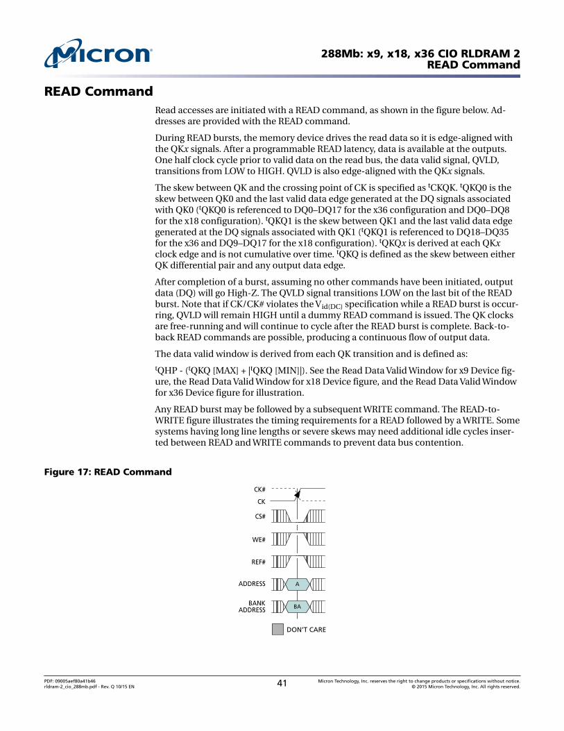
READ CommandRead accesses are initiated with a READ command, as shown in the figure below. Ad-dresses are provided with the READ command.
During READ bursts, the memory device drives the read data so it is edge-aligned withthe QKx signals. After a programmable READ latency, data is available at the outputs.One half clock cycle prior to valid data on the read bus, the data valid signal, QVLD,transitions from LOW to HIGH. QVLD is also edge-aligned with the QKx signals.
The skew between QK and the crossing point of CK is specified as tCKQK. tQKQ0 is theskew between QK0 and the last valid data edge generated at the DQ signals associatedwith QK0 (tQKQ0 is referenced to DQ0–DQ17 for the x36 configuration and DQ0–DQ8for the x18 configuration). tQKQ1 is the skew between QK1 and the last valid data edgegenerated at the DQ signals associated with QK1 (tQKQ1 is referenced to DQ18–DQ35for the x36 and DQ9–DQ17 for the x18 configuration). tQKQx is derived at each QKxclock edge and is not cumulative over time. tQKQ is defined as the skew between eitherQK differential pair and any output data edge.
After completion of a burst, assuming no other commands have been initiated, outputdata (DQ) will go High-Z. The QVLD signal transitions LOW on the last bit of the READburst. Note that if CK/CK# violates the Vid(DC) specification while a READ burst is occur-ring, QVLD will remain HIGH until a dummy READ command is issued. The QK clocksare free-running and will continue to cycle after the READ burst is complete. Back-to-back READ commands are possible, producing a continuous flow of output data.
The data valid window is derived from each QK transition and is defined as:
tQHP - (tQKQ [MAX] + |tQKQ [MIN]|). See the Read Data Valid Window for x9 Device fig-ure, the Read Data Valid Window for x18 Device figure, and the Read Data Valid Windowfor x36 Device figure for illustration.
Any READ burst may be followed by a subsequent WRITE command. The READ-to-WRITE figure illustrates the timing requirements for a READ followed by a WRITE. Somesystems having long line lengths or severe skews may need additional idle cycles inser-ted between READ and WRITE commands to prevent data bus contention.
Figure 17: READ Command
DON’T CARE
CK
CK#
CS#
WE#
REF#
A
BA
ADDRESS
BANKADDRESS
288Mb: x9, x18, x36 CIO RLDRAM 2READ Command
PDF: 09005aef80a41b46rldram-2_cio_288mb.pdf - Rev. Q 10/15 EN 41 Micron Technology, Inc. reserves the right to change products or specifications without notice.
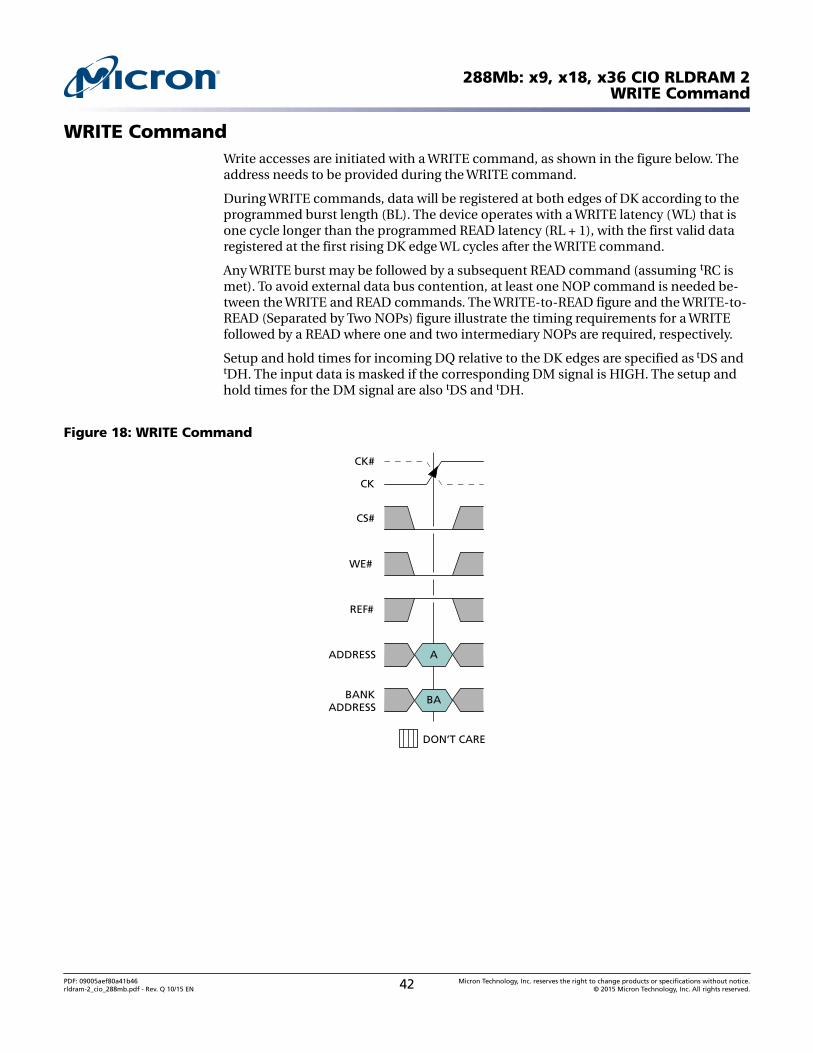
WRITE CommandWrite accesses are initiated with a WRITE command, as shown in the figure below. Theaddress needs to be provided during the WRITE command.
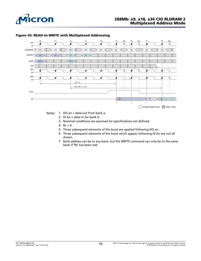
During WRITE commands, data will be registered at both edges of DK according to theprogrammed burst length (BL). The device operates with a WRITE latency (WL) that isone cycle longer than the programmed READ latency (RL + 1), with the first valid dataregistered at the first rising DK edge WL cycles after the WRITE command.
Any WRITE burst may be followed by a subsequent READ command (assuming tRC ismet). To avoid external data bus contention, at least one NOP command is needed be-tween the WRITE and READ commands. The WRITE-to-READ figure and the WRITE-to-READ (Separated by Two NOPs) figure illustrate the timing requirements for a WRITEfollowed by a READ where one and two intermediary NOPs are required, respectively.
Setup and hold times for incoming DQ relative to the DK edges are specified as tDS andtDH. The input data is masked if the corresponding DM signal is HIGH. The setup andhold times for the DM signal are also tDS and tDH.
Figure 18: WRITE Command
CK#
CK
WE#
REF#
CS#
AADDRESS
BANKADDRESS
BA
DON’T CARE
288Mb: x9, x18, x36 CIO RLDRAM 2WRITE Command
PDF: 09005aef80a41b46rldram-2_cio_288mb.pdf - Rev. Q 10/15 EN 42 Micron Technology, Inc. reserves the right to change products or specifications without notice.
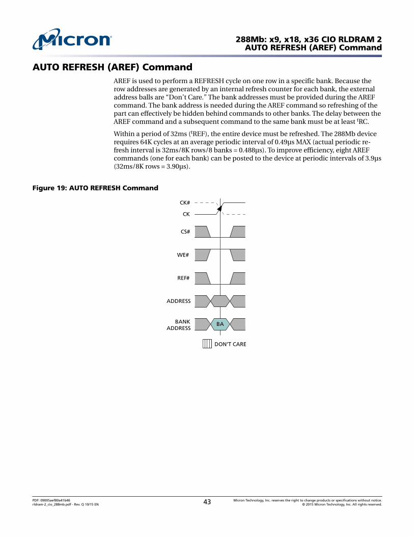
AUTO REFRESH (AREF) CommandAREF is used to perform a REFRESH cycle on one row in a specific bank. Because therow addresses are generated by an internal refresh counter for each bank, the externaladdress balls are “Don’t Care.” The bank addresses must be provided during the AREFcommand. The bank address is needed during the AREF command so refreshing of thepart can effectively be hidden behind commands to other banks. The delay between theAREF command and a subsequent command to the same bank must be at least tRC.
Within a period of 32ms (tREF), the entire device must be refreshed. The 288Mb devicerequires 64K cycles at an average periodic interval of 0.49µs MAX (actual periodic re-fresh interval is 32ms/8K rows/8 banks = 0.488µs). To improve efficiency, eight AREFcommands (one for each bank) can be posted to the device at periodic intervals of 3.9µs(32ms/8K rows = 3.90µs).
PDF: 09005aef80a41b46rldram-2_cio_288mb.pdf - Rev. Q 10/15 EN 43 Micron Technology, Inc. reserves the right to change products or specifications without notice.
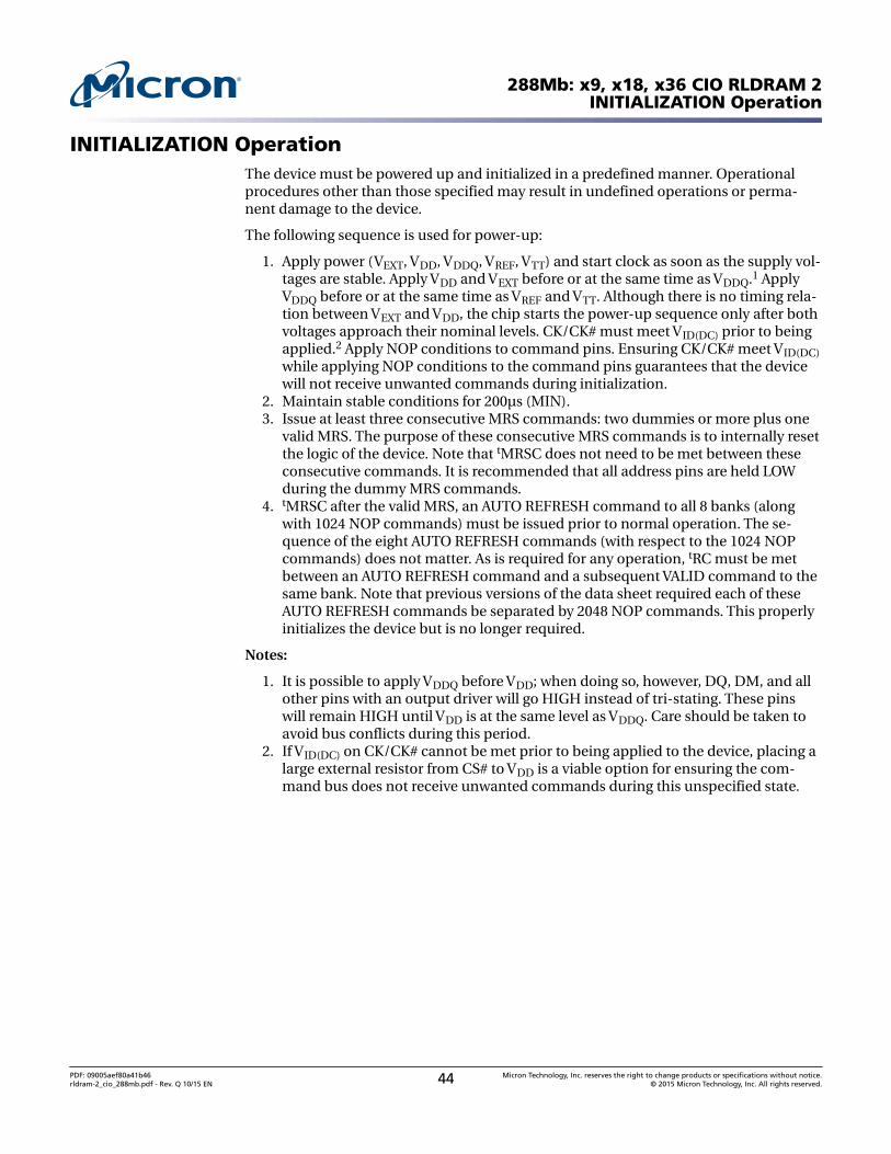
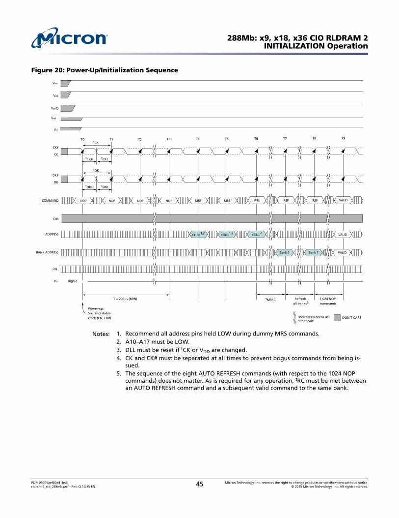
INITIALIZATION OperationThe device must be powered up and initialized in a predefined manner. Operationalprocedures other than those specified may result in undefined operations or perma-nent damage to the device.
The following sequence is used for power-up:
1. Apply power (VEXT, VDD, VDDQ, VREF, VTT) and start clock as soon as the supply vol-tages are stable. Apply VDD and VEXT before or at the same time as VDDQ.1 ApplyVDDQ before or at the same time as VREF and VTT. Although there is no timing rela-tion between VEXT and VDD, the chip starts the power-up sequence only after bothvoltages approach their nominal levels. CK/CK# must meet VID(DC) prior to beingapplied.2 Apply NOP conditions to command pins. Ensuring CK/CK# meet VID(DC)while applying NOP conditions to the command pins guarantees that the devicewill not receive unwanted commands during initialization.
2. Maintain stable conditions for 200µs (MIN).3. Issue at least three consecutive MRS commands: two dummies or more plus one
valid MRS. The purpose of these consecutive MRS commands is to internally resetthe logic of the device. Note that tMRSC does not need to be met between theseconsecutive commands. It is recommended that all address pins are held LOWduring the dummy MRS commands.
4. tMRSC after the valid MRS, an AUTO REFRESH command to all 8 banks (alongwith 1024 NOP commands) must be issued prior to normal operation. The se-quence of the eight AUTO REFRESH commands (with respect to the 1024 NOPcommands) does not matter. As is required for any operation, tRC must be metbetween an AUTO REFRESH command and a subsequent VALID command to thesame bank. Note that previous versions of the data sheet required each of theseAUTO REFRESH commands be separated by 2048 NOP commands. This properlyinitializes the device but is no longer required.
Notes:
1. It is possible to apply VDDQ before VDD; when doing so, however, DQ, DM, and allother pins with an output driver will go HIGH instead of tri-stating. These pinswill remain HIGH until VDD is at the same level as VDDQ. Care should be taken toavoid bus conflicts during this period.
2. If VID(DC) on CK/CK# cannot be met prior to being applied to the device, placing alarge external resistor from CS# to VDD is a viable option for ensuring the com-mand bus does not receive unwanted commands during this unspecified state.
PDF: 09005aef80a41b46rldram-2_cio_288mb.pdf - Rev. Q 10/15 EN 44 Micron Technology, Inc. reserves the right to change products or specifications without notice.
Notes: 1. Recommend all address pins held LOW during dummy MRS commands.2. A10–A17 must be LOW.3. DLL must be reset if tCK or VDD are changed.4. CK and CK# must be separated at all times to prevent bogus commands from being is-
sued.5. The sequence of the eight AUTO REFRESH commands (with respect to the 1024 NOP
commands) does not matter. As is required for any operation, tRC must be met betweenan AUTO REFRESH command and a subsequent valid command to the same bank.
PDF: 09005aef80a41b46rldram-2_cio_288mb.pdf - Rev. Q 10/15 EN 45 Micron Technology, Inc. reserves the right to change products or specifications without notice.
Note: 1. The sequence of the eight AUTO REFRESH commands (with respect to the 1024 NOPcommands) does not matter. As is required for any operation, tRC must be met betweenan AUTO REFRESH command and a subsequent valid command to the same bank.
PDF: 09005aef80a41b46rldram-2_cio_288mb.pdf - Rev. Q 10/15 EN 46 Micron Technology, Inc. reserves the right to change products or specifications without notice.
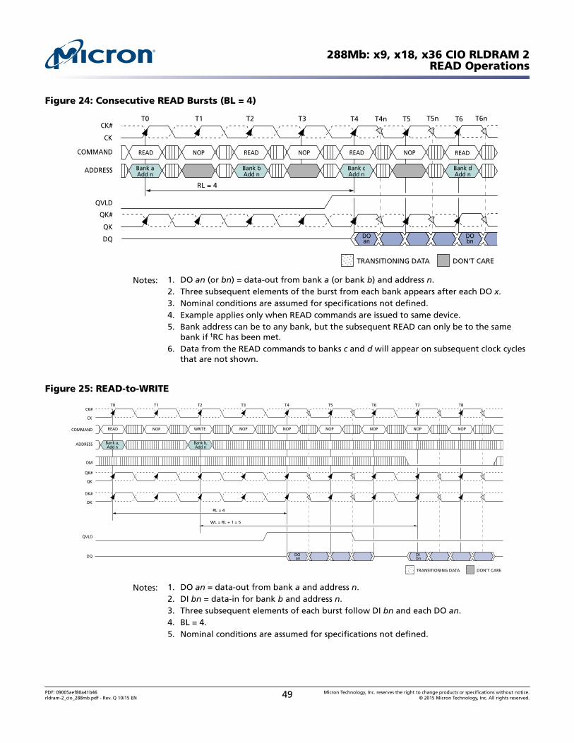
Notes: 1. DO an = data-out from bank a and address an.2. Three subsequent elements of the burst are applied following DO an.3. BL = 4.4. Nominal conditions are assumed for specifications not defined.
288Mb: x9, x18, x36 CIO RLDRAM 2READ Operations
PDF: 09005aef80a41b46rldram-2_cio_288mb.pdf - Rev. Q 10/15 EN 47 Micron Technology, Inc. reserves the right to change products or specifications without notice.
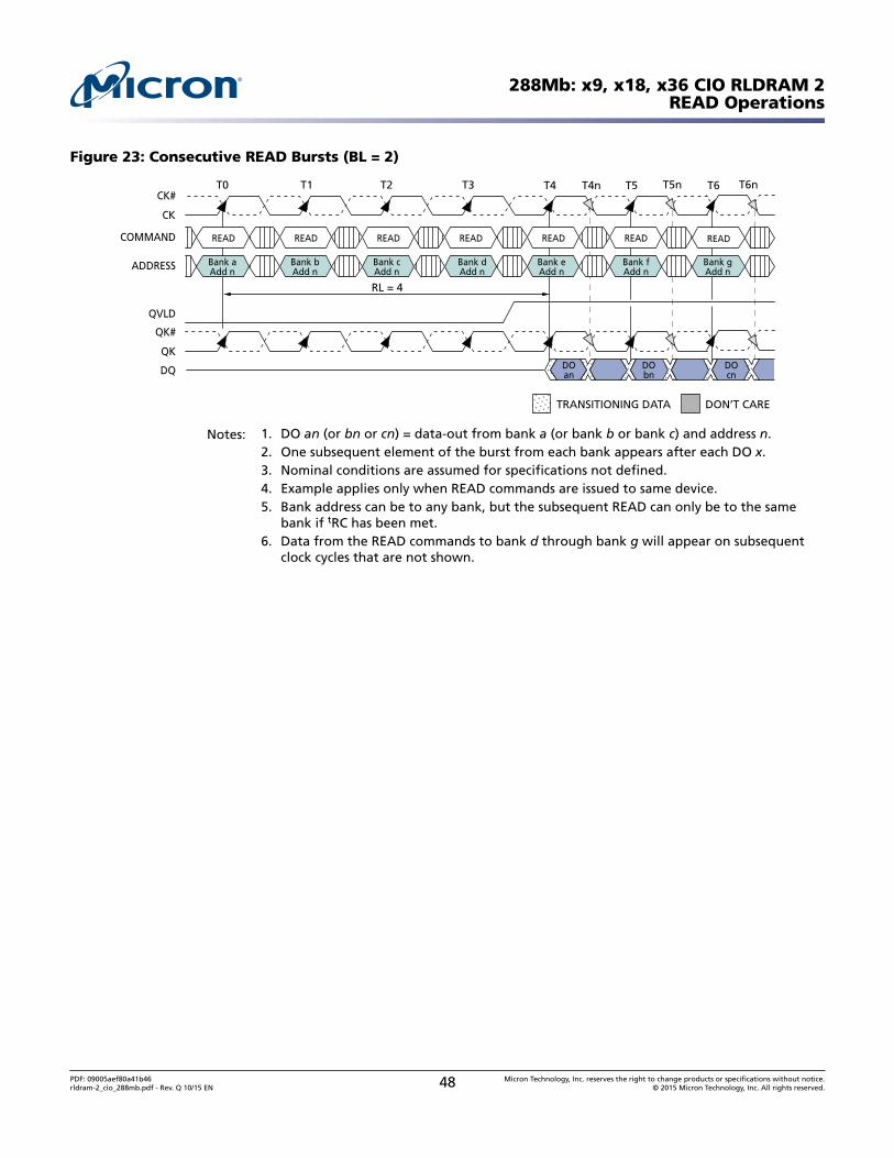
Notes: 1. DO an (or bn or cn) = data-out from bank a (or bank b or bank c) and address n.2. One subsequent element of the burst from each bank appears after each DO x.3. Nominal conditions are assumed for specifications not defined.4. Example applies only when READ commands are issued to same device.5. Bank address can be to any bank, but the subsequent READ can only be to the same
bank if tRC has been met.6. Data from the READ commands to bank d through bank g will appear on subsequent
clock cycles that are not shown.
288Mb: x9, x18, x36 CIO RLDRAM 2READ Operations
PDF: 09005aef80a41b46rldram-2_cio_288mb.pdf - Rev. Q 10/15 EN 48 Micron Technology, Inc. reserves the right to change products or specifications without notice.
Notes: 1. DO an (or bn) = data-out from bank a (or bank b) and address n.2. Three subsequent elements of the burst from each bank appears after each DO x.3. Nominal conditions are assumed for specifications not defined.4. Example applies only when READ commands are issued to same device.5. Bank address can be to any bank, but the subsequent READ can only be to the same
bank if tRC has been met.6. Data from the READ commands to banks c and d will appear on subsequent clock cycles
that are not shown.
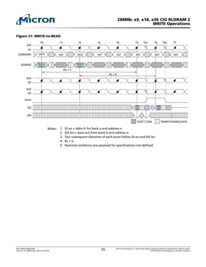
Figure 25: READ-to-WRITE
CK
CK#
COMMAND
ADDRESS
QVLD
DQ
READ
T0 T1 T2
DON’T CARETRANSITIONING DATA
WRITE NOP
T3 T4 T5
NOP NOP
T6
NOP
WL = RL + 1 = 5
T7 T8
NOP NOP
DK
DK#
QK
DM
QK#
DO an
DI bn
RL = 4
Bank a,Add n
Bank b,Add n
NOP NOP
Notes: 1. DO an = data-out from bank a and address n.2. DI bn = data-in for bank b and address n.3. Three subsequent elements of each burst follow DI bn and each DO an.4. BL = 4.5. Nominal conditions are assumed for specifications not defined.
288Mb: x9, x18, x36 CIO RLDRAM 2READ Operations
PDF: 09005aef80a41b46rldram-2_cio_288mb.pdf - Rev. Q 10/15 EN 49 Micron Technology, Inc. reserves the right to change products or specifications without notice.
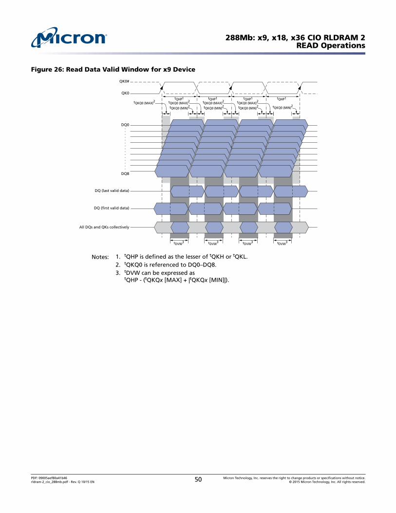
Notes: 1. tQHP is defined as the lesser of tQKH or tQKL.2. tQKQ0 is referenced to DQ0–DQ8.3. tDVW can be expressed as
tQHP - (tQKQx [MAX] + |tQKQx [MIN]|).
288Mb: x9, x18, x36 CIO RLDRAM 2READ Operations
PDF: 09005aef80a41b46rldram-2_cio_288mb.pdf - Rev. Q 10/15 EN 50 Micron Technology, Inc. reserves the right to change products or specifications without notice.
Notes: 1. tQHP is defined as the lesser of tQKH or tQKL.2. tQKQ0 is referenced to DQ0–DQ8.3. tDVW can be expressed as
tQHP - (tQKQx [MAX] + |tQKQx [MIN]|).4. tQKQ1 is referenced to DQ9–DQ17.5. tQKQ takes into account the skew between any QKx and any DQ.
288Mb: x9, x18, x36 CIO RLDRAM 2READ Operations
PDF: 09005aef80a41b46rldram-2_cio_288mb.pdf - Rev. Q 10/15 EN 51 Micron Technology, Inc. reserves the right to change products or specifications without notice.
Notes: 1. tQHP is defined as the lesser of tQKH or tQKL.2. tQKQ0 is referenced to DQ0–DQ17.3. tDVW can be expressed as
tQHP - (tQKQx [MAX] + |tQKQx [MIN]|).4. tQKQ1 is referenced to DQ18–DQ35.5. tQKQ takes into account the skew between any QKx and any DQ.
288Mb: x9, x18, x36 CIO RLDRAM 2READ Operations
PDF: 09005aef80a41b46rldram-2_cio_288mb.pdf - Rev. Q 10/15 EN 52 Micron Technology, Inc. reserves the right to change products or specifications without notice.
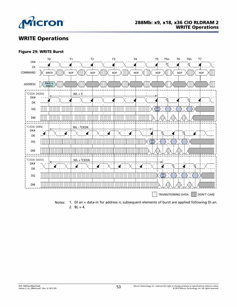
Notes: 1. DI an = data-in for address n; subsequent elements of burst are applied following DI an.2. BL = 4.
288Mb: x9, x18, x36 CIO RLDRAM 2WRITE Operations
PDF: 09005aef80a41b46rldram-2_cio_288mb.pdf - Rev. Q 10/15 EN 53 Micron Technology, Inc. reserves the right to change products or specifications without notice.
Notes: 1. DI an (or bn) = data-in for bank a (or bank b) and address n.2. Three subsequent elements of the burst are applied following DI for each bank.3. BL = 4.4. Each WRITE command may be to any bank; if the second WRITE is to the same bank,
tRC must be met.5. Nominal conditions are assumed for specifications not defined.
288Mb: x9, x18, x36 CIO RLDRAM 2WRITE Operations
PDF: 09005aef80a41b46rldram-2_cio_288mb.pdf - Rev. Q 10/15 EN 54 Micron Technology, Inc. reserves the right to change products or specifications without notice.
Notes: 1. DI an = data-in for bank a and address n.2. DO bn = data-out from bank b and address n.3. Two subsequent elements of each burst follow DI an and DO bn.4. BL = 2.5. Nominal conditions are assumed for specifications not defined.
288Mb: x9, x18, x36 CIO RLDRAM 2WRITE Operations
PDF: 09005aef80a41b46rldram-2_cio_288mb.pdf - Rev. Q 10/15 EN 55 Micron Technology, Inc. reserves the right to change products or specifications without notice.
Figure 32: WRITE-to-READ – Separated by Two NOP Commands
COMMAND NOP NOP READ NOP NOPNOP
ADDRESS Bank a,Add n
CK
CK#T0 T1 T2 T3 T4 T5 T5n T6 T7nT7 T8
DQ
DM
DIan
DObn
DON’T CARETRANSITIONING DATA
WL = 5
QVLD
DK#
DK
QK#QK
NOP NOP
Bank b,Add n
WRITE
RL = 4
tQKQ (MIN)
tCKQK (MIN)
tCKDK (MAX)
tDH
Notes: 1. DI an = data-in for bank a and address n.2. DO bn = data-out from bank b and address n.3. One subsequent element of each burst follow DI an and DO bn.4. BL = 2.5. Only one NOP separating the WRITE and READ would have led to contention on the da-
ta bus because of the input and output data timing conditions being used.6. Nominal conditions are assumed for specifications not defined.
288Mb: x9, x18, x36 CIO RLDRAM 2WRITE Operations
PDF: 09005aef80a41b46rldram-2_cio_288mb.pdf - Rev. Q 10/15 EN 56 Micron Technology, Inc. reserves the right to change products or specifications without notice.
Notes: 1. DI n = data-in from address n.2. Subsequent elements of burst are provided on following clock edges.3. BL = 4.4. Nominal conditions are assumed for specifications not defined.
288Mb: x9, x18, x36 CIO RLDRAM 2WRITE Operations
PDF: 09005aef80a41b46rldram-2_cio_288mb.pdf - Rev. Q 10/15 EN 57 Micron Technology, Inc. reserves the right to change products or specifications without notice.
Notes: 1. AREFx = AUTO REFRESH command to bank x.2. ACx = any command to bank x; ACy = any command to bank y.3. BAx = bank address to bank x; BAy = bank address to bank y.
PDF: 09005aef80a41b46rldram-2_cio_288mb.pdf - Rev. Q 10/15 EN 58 Micron Technology, Inc. reserves the right to change products or specifications without notice.
Notes: 1. DO n = data out from bank a and address n.2. DO n is followed by the remaining bits of the burst.3. Nominal conditions are assumed for specifications not defined.
PDF: 09005aef80a41b46rldram-2_cio_288mb.pdf - Rev. Q 10/15 EN 59 Micron Technology, Inc. reserves the right to change products or specifications without notice.
Notes: 1. DO an (or bn) = data-out from bank a (or bank b) and address n.2. BL = 2.3. One subsequent element of the burst appears after DO an and DO bn.4. Nominal conditions are assumed for specifications not defined.
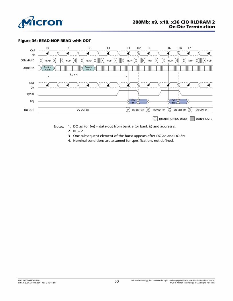
PDF: 09005aef80a41b46rldram-2_cio_288mb.pdf - Rev. Q 10/15 EN 60 Micron Technology, Inc. reserves the right to change products or specifications without notice.
Notes: 1. DO an = data-out from bank a and address n; DI bn = data-in for bank b and address n.2. BL = 2.3. One subsequent element of each burst appears after each DO an and DI bn.4. Nominal conditions are assumed for specifications not defined.
PDF: 09005aef80a41b46rldram-2_cio_288mb.pdf - Rev. Q 10/15 EN 61 Micron Technology, Inc. reserves the right to change products or specifications without notice.
PDF: 09005aef80a41b46rldram-2_cio_288mb.pdf - Rev. Q 10/15 EN 62 Micron Technology, Inc. reserves the right to change products or specifications without notice.
Figure 39: Power-Up/Initialization Sequence in Multiplexed Address Mode
BANKADDRESS
Power-up:VDD and stableclock (CK, CK#)
T = 200µs (MIN)
High-Z
DM
()()
()()
ADDRESS
COMMAND NOPNOPNOP
()()
()()
()()
()()
DON’T CARE
VEXT
D High-Z
tMRSC tMRSC Refreshall banks9
1024 NOPcommands
()()
()()
()()
()()
MRS MRS
CODE2,3 Ax2,4()()
()()
()()
()()
()()
()()
()()
()()
()()
()()
()()
()()
MRSMRS
CODE1,2 CODE1,2
()()
()()
VALID5
VALID5
VALID5
CK
CK#
tCKL
T0 T1 T2
tCKH
tCKT3
()()
T8 T9 T10 T11T6 T7T4 T5
()()
()()
DK
DK#
tDKLtDKH
tDK()()
()()
()()
()()
NOP
()()
()()
Q High-Z ()()
()()
()()
()()
()()
()()
()()
Bank 7
()()
()()
()()
()()
()()
()()
NOP REF REF
()()
()()
()()
()()
Ay
Bank 0
()()
()()
()()
()()
()()
()()
()()
()()
()()
()()
()()
()()
()()
()()
()()
()()
()()
()()
()()
()()
()()
()()
()()
()()
()()
Indicates a break in time scale
VDD
VDDQ
VREF
VTT
RTT
Notes: 1. Recommended that all address pins held LOW during dummy MRS commands.2. A10–A18 must be LOW.3. Set address A5 HIGH. This enables the part to enter multiplexed address mode when in
non-multiplexed mode operation. Multiplexed address mode can also be entered atsome later time by issuing an MRS command with A5 HIGH. Once address bit A5 is setHIGH, tMRSC must be satisfied before the two-cycle multiplexed mode MRS command isissued.
4. Address A5 must be set HIGH. This and the following step set the desired mode registeronce the device is in multiplexed address mode.
5. Any command or address.6. The above sequence must be followed in order to power up the device in the multi-
plexed address mode.7. DLL must be reset if tCK or VDD are changed.8. CK and CK# must separated at all times to prevent bogus commands from being issued.9. The sequence of the eight AUTO REFRESH commands (with respect to the 1024 NOP
commands) does not matter. As is required for any operation, tRC must be met betweenan AUTO REFRESH command and a subsequent VALID command to the same bank.
PDF: 09005aef80a41b46rldram-2_cio_288mb.pdf - Rev. Q 10/15 EN 63 Micron Technology, Inc. reserves the right to change products or specifications without notice.
Figure 40: Mode Register Definition in Multiplexed Address Mode
2 1 03458918–10 7 6
ConfigBLAMReserved1Mode Register (Mx)
Configuration
12 (default)
12
2
3
42
5
Reserved
Reserved
M1
0
0
1
1
0
0
1
1
M2
0
0
0
0
1
1
1
1
M5
0
1
Address MUX
Nonmultiplexed (default)
Multiplexed
M8
0
1
Drive Impedance
Internal 50Ω3 (default)
External (ZQ)
M9
0
1
On-Die Termination
Off (default)
On
DLL NA5
M7
0
1
DLL Reset
DLL reset4 (default)
DLL enabled
ODT
M3
0
1
0
1
Burst Length
2 (default)
4
8
Reserved
M4
0
0
1
1
IM
M0
0
1
0
1
0
1
0
1
A3A4A8A9Ay . . .A18A0A3A4A5A8A9Ax
A10. . .A18 A10
Notes: 1. Bits A10–A18 must be set to zero.2. BL = 8 is not available.3. ±30% temperature variation.4. DLL RESET turns the DLL off.5. Ay8 not used in MRS.6. BA0–BA2 are “Don’t Care.”7. Addresses A0, A3, A4, A5, A8, and A9 must be set as shown in order to activate the
PDF: 09005aef80a41b46rldram-2_cio_288mb.pdf - Rev. Q 10/15 EN 64 Micron Technology, Inc. reserves the right to change products or specifications without notice.
PDF: 09005aef80a41b46rldram-2_cio_288mb.pdf - Rev. Q 10/15 EN 65 Micron Technology, Inc. reserves the right to change products or specifications without notice.
In multiplexed address mode, the READ and WRITE latencies are increased by oneclock cycle. However, the device cycle time remains the same as when in nonmulti-plexed address mode.
Table 25: Cycle Time and READ/WRITE Latency Configuration in Multiplexed Mode
Valid frequency range 266–175 400–175 533–175 200–175 333–175 MHz
Notes: 1. tRC <20ns in any configuration is only available with -25E and -18 speed grades.2. BL = 8 is not available.3. The minimum tRC is typically 3 cycles, except in the case of a WRITE followed by a READ
to the same bank. In this instance the minimum tRC is 4 cycles.
REFRESH Command in Multiplexed Address Mode
Similar to other commands when in multiplexed address mode, AREF is executed onthe rising clock edge following the one on which the command is issued. However, be-cause only the bank address is required for AREF, the next command can be applied onthe following clock. The operation of the AREF command and any other command isrepresented in the following figure.
Figure 41: Burst REFRESH Operation with Multiplexed Addressing
CK
CK#
COMMAND AC1 NOP
Ay
AREF AREF AREF AREFAREF AREF AREF AREF AC1
BANK Bank 0Bank n Bank 1 Bank 2 Bank 3 Bank 4 Bank 5 Bank 6 Bank 7 Bank n
ADDRESS Ax AyAx
T0 T1 T2 T3 T4 T5 T6 T7 T8 T9 T10 T11
DON’T CARE
Notes: 1. Any command.2. Bank n is chosen so that tRC is met.
PDF: 09005aef80a41b46rldram-2_cio_288mb.pdf - Rev. Q 10/15 EN 66 Micron Technology, Inc. reserves the right to change products or specifications without notice.
Figure 42: Consecutive WRITE Bursts with Multiplexed Addressing
CK
CK#
COMMAND WRITE NOP
Ay
WRITE WRITE NOP NOP NOP NOP NOP
BANK Bank a
Ay
NOP
Bank b Bank a1
ADDRESS Ax Ax Ax Ay
T0 T1 T2 T3 T4 T5 T6 T6n T7 T8 T9T8nT7n
D
DM
DIb
DIa
DON’T CARETRANSITIONING DATA
WL = 6
tRC = 4DK
DK#
Notes: 1. Data from the second WRITE command to bank a will appear on subsequent clock cyclesthat are not shown.
2. DI a = data-in for bank a; DI b = data-in for bank b.3. Three subsequent elements of the burst are applied following DI for each bank.4. Each WRITE command may be to any bank; if the second WRITE is to the same bank, tRC
PDF: 09005aef80a41b46rldram-2_cio_288mb.pdf - Rev. Q 10/15 EN 67 Micron Technology, Inc. reserves the right to change products or specifications without notice.
Figure 43: WRITE-to-READ with Multiplexed Addressing
COMMAND NOP READ NOP NOPNOP
ADDRESS Ax Ay
NOP
CK
CK#T0 T1 T2 T3 T4 T5 T6 T6n T7nT7
DM
DON’T CARETRANSITIONING DATA
WL = 6
QVLD
DK#
DK
QK#
QK
NOP
BANK Bank a Bank b
WRITE
RL = 5
DQDIa
Ax Ay
DOb
Notes: 1. DI a = data-in for bank a.2. DO b = data-out from bank b.3. One subsequent element of each burst follows DI a and DO b.4. BL = 2.5. Nominal conditions are assumed for specifications not defined.6. Bank address can be to any bank, but the subsequent READ can only be to the same
PDF: 09005aef80a41b46rldram-2_cio_288mb.pdf - Rev. Q 10/15 EN 68 Micron Technology, Inc. reserves the right to change products or specifications without notice.
Figure 44: Consecutive READ Bursts with Multiplexed Addressing
COMMAND READ NOP READ NOP READ NOP
ADDRESS Ax Ay
Bank a
CK
CK#
QK
QK#
BANK
QVLD
DQ
RL = 5
DOa
T0 T1 T2 T3
READ
T4 T5 T6T5n T6n
DON’T CARETRANSITIONING DATA
Bank b Bank c Bank d
Ax Ax AxAy Ay
Notes: 1. DO a = data-out from bank a.2. Nominal conditions are assumed for specifications not defined.3. BL = 4.4. Three subsequent elements of the burst appear following DO a.5. Example applies only when READ commands are issued to same device.6. Bank address can be to any bank, but the subsequent READ can only be to the same
bank if tRC has been met.7. Data from the READ commands to banks b through bank d will appear on subsequent
PDF: 09005aef80a41b46rldram-2_cio_288mb.pdf - Rev. Q 10/15 EN 69 Micron Technology, Inc. reserves the right to change products or specifications without notice.
Figure 45: READ-to-WRITE with Multiplexed Addressing
CK
CK#
COMMAND
ADDRESS
BANK
QVLD
DQ
READ
T0 T1 T2
DON’T CARETRANSITIONING DATA
WRITE NOP
T3 T4 T5 T5n
NOP NOP
T6 T6n
NOP
WL = RL + 1 = 6
T7 T8 T8n
NOP NOP
DK
DK#
QK
DM
QK#
DO an
DI bn
RL = 5
Ax Ay Ay
Bank a
Ax
Bank b
NOP NOP
Notes: 1. DO an = data-out from bank a.2. DI bn = data-in for bank b.3. Nominal conditions are assumed for specifications not defined.4. BL = 4.5. Three subsequent elements of the burst are applied following DO an.6. Three subsequent elements of the burst which appear following DI bn are not all
shown.7. Bank address can be to any bank, but the WRITE command can only be to the same
PDF: 09005aef80a41b46rldram-2_cio_288mb.pdf - Rev. Q 10/15 EN 70 Micron Technology, Inc. reserves the right to change products or specifications without notice.
IEEE 1149.1 Serial Boundary Scan (JTAG)RLDRAM incorporates a serial boundary-scan test access port (TAP) for testing connec-tivity once it has been mounted on a printed circuit board (PCB). As the complexity ofPCB high-density surface mounting techniques increase, the boundary-scan architec-ture is a valuable resource for interconnectivity debug. This port operates in accordancewith IEEE Standard 1149.1-2001 (JTAG) with the exception of the ZQ pin. To ensureproper boundary-scan testing of the ZQ pin, MRS bit M8 needs to be set to 0 until theJTAG testing of the pin is complete.
Note: Upon power up, the default state of MRS bit M8 is LOW.
If the device boundary scan register is to be used upon power-up and prior to deviceinitialization, it is imperative that the CK and CK# pins meet VID(DC) or CS# be heldHIGH from power up until testing. Not doing so could result in inadvertent MRS com-mands being loaded and subsequently causing unexpected results from address pinsthat are dependent upon the state of the mode register. If these measures cannot be tak-en, the part must be initialized prior to boundary scan testing. If a full initialization isnot practical or feasible prior to boundary scan testing, a single MRS command with de-sired settings may be issued instead. After the single MRS command is issued, thetMRSC parameter must be satisfied prior to boundary scan testing.
The input signals of the test access port (TDI, TMS, and TCK) use V DD as a supply, whilethe output signal of the TAP (TDO) uses VDDQ.
The JTAG test access port utilizes the device TAP controller, from which the instructionregister, boundary scan register, bypass register, and ID register can be selected.
Disabling the JTAG Feature
It is possible to operate the device without using the JTAG feature. To disable the TAPcontroller, TCK must be tied LOW (VSS) to prevent clocking of the device. TDI and TMSare internally pulled up and may be unconnected. They may alternately be connectedto VDD through a pull-up resistor. TDO should be left unconnected. Upon power-up, thedevice will come up in a reset state, which will not interfere with the operation of thedevice.
Test Access Port (TAP)
Test Clock (TCK)
The test clock is used only with the TAP controller. All inputs are captured on the risingedge of TCK. All outputs are driven from the falling edge of TCK.
Test Mode Select (TMS)
The TMS input is used to give commands to the TAP controller and is sampled on therising edge of TCK.
All of the states in the TAP Controller State Diagram are entered through the serial inputof the TMS pin. A 0 in the diagram represents a LOW on the TMS pin during the risingedge of TCK while a 1 represents a HIGH on TMS.
PDF: 09005aef80a41b46rldram-2_cio_288mb.pdf - Rev. Q 10/15 EN 71 Micron Technology, Inc. reserves the right to change products or specifications without notice.
The TDI ball is used to serially input test instructions and data into the registers and canbe connected to the input of any of the registers. The register between TDI and TDO ischosen by the instruction that is loaded into the TAP instruction register. For informa-tion on loading the instruction register, see TAP Controller State Diagram. TDI is con-nected to the most significant bit (MSB) of any register (see TAP Controller Block Dia-gram).
Test Data-Out (TDO)
The TDO output ball is used to serially clock test instructions and data out from the reg-isters. The TDO output driver is only active during the Shift-IR and Shift-DR TAP con-troller states. In all other states, the TDO pin is in a High-Z state. The output changes onthe falling edge of TCK. TDO is connected to the least significant bit (LSB) of any regis-ter (see the TAP Controller Block Diagram).
288Mb: x9, x18, x36 CIO RLDRAM 2Test Access Port (TAP)
PDF: 09005aef80a41b46rldram-2_cio_288mb.pdf - Rev. Q 10/15 EN 72 Micron Technology, Inc. reserves the right to change products or specifications without notice.
TAP ControllerThe TAP controller is a finite state machine that uses the state of the TMS pin at the ris-ing edge of TCK to navigate through its various modes of operation. See the TAP Con-troller State Diagram.
Test-Logic-Reset
The test-logic-reset controller state is entered when TMS is held HIGH for at least fiveconsecutive rising edges of TCK. As long as TMS remains HIGH, the TAP controller willremain in the test-logic-reset state. The test logic is inactive during this state.
Run-Test/Idle
The run-test/idle is a controller state in-between scan operations. This state can bemaintained by holding TMS LOW. From here either the data register scan, or subse-quently, the instruction register scan, can be selected.
Select-DR-Scan
Select-DR-scan is a temporary controller state. All test data registers retain their previ-ous state while here.
Capture-DR
The capture-DR state is where the data is parallel-loaded into the test data registers. Ifthe boundary scan register is the currently selected register, then the data currently onthe pins is latched into the test data registers.
Shift-DR
Data is shifted serially through the data register while in this state. As new data is inputthrough the TDI pin, data is shifted out of the TDO pin.
Exit1-DR, Pause-DR, and Exit2-DR
The purpose of exit1-DR is used to provide a path to return back to the run-test/idlestate (through the update-DR state). The pause-DR state is entered when the shifting ofdata through the test registers needs to be suspended. When shifting is to reconvene,the controller enters the exit2-DR state and then can re-enter the shift-DR state.
Update-DR
When the EXTEST instruction is selected, there are latched parallel outputs of the boun-dary-scan shift register that only change state during the update-DR controller state.
Instruction Register States
The instruction register states of the TAP controller are similar to the data registerstates. The desired instruction is serially shifted into the instruction register during theshift-IR state and is loaded during the update-IR state.
288Mb: x9, x18, x36 CIO RLDRAM 2TAP Controller
PDF: 09005aef80a41b46rldram-2_cio_288mb.pdf - Rev. Q 10/15 EN 73 Micron Technology, Inc. reserves the right to change products or specifications without notice.
TAP ResetA reset is performed by forcing TMS HIGH (VDDQ) for five rising edges of TCK. The resetdoes not affect the operation of the device and may be performed while it is operating.At power-up, the TAP is reset internally to ensure that TDO comes up in a High-Z state.
288Mb: x9, x18, x36 CIO RLDRAM 2TAP Reset
PDF: 09005aef80a41b46rldram-2_cio_288mb.pdf - Rev. Q 10/15 EN 74 Micron Technology, Inc. reserves the right to change products or specifications without notice.
TAP RegistersRegisters are connected between the TDI and TDO balls and allow data to be scannedinto and out of the device test circuitry. Only one register can be selected at a timethrough the instruction register. Data is serially loaded into the TDI ball on the risingedge of TCK. Data is output on the TDO ball on the falling edge of TCK.
Instruction Register
Eight-bit instructions can be serially loaded into the instruction register. This register isloaded during the update-IR state of the TAP controller. Upon power-up, the instructionregister is loaded with the IDCODE instruction. It is also loaded with the IDCODE in-struction if the controller is placed in a reset state as described in the previous section.
When the TAP controller is in the capture-IR state, the two least significant bits are loa-ded with a binary 01 pattern to allow for fault isolation of the board-level serial test datapath.
Bypass Register
To save time when serially shifting data through registers, it is sometimes advantageousto skip certain chips. The bypass register is a single-bit register that can be placed be-tween the TDI and TDO balls. This allows data to be shifted through the device withminimal delay. The bypass register is set LOW (VSS) when the BYPASS instruction is exe-cuted.
Boundary Scan Register
The boundary scan register is connected to all the input and bidirectional balls on thedevice. Several balls are also included in the scan register to reserved balls. The devicehas a 113-bit register.
The boundary scan register is loaded with the contents of the RAM I/O ring when theTAP controller is in the capture-DR state and is then placed between the TDI and TDOballs when the controller is moved to the shift-DR state.
The Boundary Scan (Exit) Order table shows the order in which the bits are connected.Each bit corresponds to one of the balls on the device package. The most significant bitof the register is connected to TDI, and the least significant bit is connected to TDO.
Identification (ID) Register
The ID register is loaded with a vendor-specific, 32-bit code during the capture-DRstate when the IDCODE command is loaded in the instruction register. The IDCODE ishardwired into the device and can be shifted out when the TAP controller is in the shift-DR state. The ID register has a vendor code and other information described in theIdentification Register Definitions table.
288Mb: x9, x18, x36 CIO RLDRAM 2TAP Registers
PDF: 09005aef80a41b46rldram-2_cio_288mb.pdf - Rev. Q 10/15 EN 75 Micron Technology, Inc. reserves the right to change products or specifications without notice.
TAP Instruction SetMany different TAP instructions (28) are possible with the 8-bit instruction register. Allcombinations used are listed in the table below, followed by detailed descriptions. Re-maining instructions are reserved and should not be used. The TAP controller used isfully compliant to the 1149.1 convention.
Instructions are loaded into the TAP controller during the shift-IR state when the in-struction register is placed between TDI and TDO. During this state, instructions areshifted through the instruction register through the TDI and TDO balls. To execute theinstruction once it is shifted in, the TAP controller needs to be moved into the update-IR state.
Table 26: Instruction Codes
Instruction Code Description
EXTEST 0000 0000 Captures I/O ring contents; Places the boundary scan register between TDI and TDO;This operation does not affect device operations
IDCODE 0010 0001 Loads the ID register with the vendor ID code and places the register between TDIand TDO; This operation does not affect device operations
SAMPLE/PRELOAD 0000 0101 Captures I/O ring contents; Places the boundary scan register between TDI and TDO
CLAMP 0000 0111 Selects the bypass register to be connected between TDI and TDO; Data driven byoutput balls are determined from values held in the boundary scan register
High-Z 0000 0011 Selects the bypass register to be connected between TDI and TDO; All outputs areforced into High-Z
BYPASS 1111 1111 Places the bypass register between TDI and TDO; This operation does not affect de-vice operations
EXTEST
The EXTEST instruction allows circuitry external to the component package to be tes-ted. Boundary-scan register cells at output balls are used to apply a test vector, whilethose at input balls capture test results. Typically, the first test vector to be applied usingthe EXTEST instruction will be shifted into the boundary scan register using the PRE-LOAD instruction. Thus, during the update-IR state of EXTEST, the output driver isturned on, and the PRELOAD data is driven onto the output balls.
IDCODE
The IDCODE instruction causes a vendor-specific, 32-bit code to be loaded into the in-struction register. It also places the instruction register between the TDI and TDO ballsand allows the IDCODE to be shifted out of the device when the TAP controller entersthe shift-DR state. The IDCODE instruction is loaded into the instruction register uponpower-up or whenever the TAP controller is given a test logic reset state.
SAMPLE/PRELOAD
When the SAMPLE/PRELOAD instruction is loaded into the instruction register and theTAP controller is in the capture-DR state, a snapshot of data on the inputs and bidirec-tional balls is captured in the boundary scan register.
288Mb: x9, x18, x36 CIO RLDRAM 2TAP Instruction Set
PDF: 09005aef80a41b46rldram-2_cio_288mb.pdf - Rev. Q 10/15 EN 76 Micron Technology, Inc. reserves the right to change products or specifications without notice.
The user must be aware that the TAP controller clock can only operate at a frequency upto 50 MHz, while the RLDRAM clock operates significantly faster. Because there is alarge difference between the clock frequencies, it is possible that during the capture-DRstate, an input or output will undergo a transition. The TAP may then try to capture asignal while in transition (metastable state). This will not harm the device, but there isno guarantee as to the value that will be captured. Repeatable results may not be possi-ble.
To ensure that the boundary scan register will capture the correct value of a signal, thesignal must be stabilized long enough to meet the TAP controller’s capture setup plushold time (tCS plus tCH). The RLDRAM clock input might not be captured correctly ifthere is no way in a design to stop (or slow) the clock during a SAMPLE/PRELOAD in-struction. If this is an issue, it is still possible to capture all other signals and simply ig-nore the value of the CK and CK# captured in the boundary scan register.
Once the data is captured, it is possible to shift out the data by putting the TAP into theshift-DR state. This places the boundary scan register between the TDI and TDO balls.
CLAMP
When the CLAMP instruction is loaded into the instruction register, the data driven bythe output balls are determined from the values held in the boundary scan register.
High-Z
The High-Z instruction causes the boundary scan register to be connected between theTDI and TDO. This places all outputs into a High-Z state.
BYPASS
When the BYPASS instruction is loaded in the instruction register and the TAP is placedin a shift-DR state, the bypass register is placed between TDI and TDO. The advantageof the BYPASS instruction is that it shortens the boundary scan path when multiple de-vices are connected together on a board.
Reserved for Future Use
The remaining instructions are not implemented but are reserved for future use. Do notuse these instructions.
288Mb: x9, x18, x36 CIO RLDRAM 2TAP Instruction Set
PDF: 09005aef80a41b46rldram-2_cio_288mb.pdf - Rev. Q 10/15 EN 77 Micron Technology, Inc. reserves the right to change products or specifications without notice.
288Mb: x9, x18, x36 CIO RLDRAM 2TAP Instruction Set
PDF: 09005aef80a41b46rldram-2_cio_288mb.pdf - Rev. Q 10/15 EN 78 Micron Technology, Inc. reserves the right to change products or specifications without notice.
0°C ≤ TC ≤ +95°C; +1.7V ≤ VDD ≤ +1.9V, unless otherwise notedDescription Symbol Min Max Units
Input high (logic 1) voltage VIH VREF + 0.3 – V
Input low (logic 0) voltage VIL – VREF - 0.3 V
Note: 1. All voltages referenced to Vss (GND).
Table 28: TAP AC Electrical Characteristics
0°C ≤ TC ≤ +95°C; +1.7V ≤ VDD ≤ +1.9VDescription Symbol Min Max Units
Clock
Clock cycle time tTHTH 20 ns
Clock frequency fTF 50 MHz
Clock HIGH time tTHTL 10 ns
Clock LOW time tTLTH 10 ns
TDI/TDO times
TCK LOW to TDO unknown tTLOX 0 ns
TCK LOW to TDO valid tTLOV 10 ns
TDI valid to TCK HIGH tDVTH 5 ns
TCK HIGH to TDI invalid tTHDX 5 ns
Setup times
TMS setup tMVTH 5 ns
Capture setup tCS 5 ns
Hold times
TMS hold tTHMX 5 ns
Capture hold tCH 5 ns
Note: 1. tCS and tCH refer to the setup and hold time requirements of latching data from theboundary scan register.
288Mb: x9, x18, x36 CIO RLDRAM 2TAP Instruction Set
PDF: 09005aef80a41b46rldram-2_cio_288mb.pdf - Rev. Q 10/15 EN 79 Micron Technology, Inc. reserves the right to change products or specifications without notice.
Table 29: TAP DC Electrical Characteristics and Operating Conditions
0°C ≤ TC ≤ +95°C; +1.7V ≤ VDD ≤ +1.9V, unless otherwise notedDescription Condition Symbol Min Max Units Notes
Input high (logic 1) voltage – VIH VREF + 0.15 VDD + 0.3 V 1, 2
Input low (logic 0) voltage – VIL VSSQ - 0.3 VREF - 0.15 V 1, 2
Input leakage current 0V ≤ VIN ≤ VDD ILI –5.0 5.0 µA
Output leakage current Output disabled, 0V ≤ VIN ≤VDDQ
ILO –5.0 5.0 µA
Output low voltage IOLc = 100µA VOL1 0.2 V 1
Output low voltage IOLt = 2mA VOL2 0.4 V 1
Output high voltage |IOHc| = 100µA VOH1 VDDQ - 0.2 V 1
Output high voltage |IOHt| = 2mA VOH2 VDDQ - 0.4 V 1
Notes: 1. All voltages referenced to Vss (GND).2. Overshoot = VIH(AC) ≤ VDD + 0.7V for t ≤ tCK/2; undershoot = VIL(AC) ≥ –0.5V for t ≤ tCK/2;
during normal operation, VDDQ must not exceed VDD.
Table 30: Identification Register Definitions
Instruction Field All Devices Description
Revision number (31:28) abcd ab = 00 for Die Rev. A, 01 for Die Rev. B;cd = 00 for x9, 01 for x18, 10 for x36
Device ID (27:12) 00jkidef10100111 def = 000 for 288Mb, 001 for 576Mb;i = 0 for common I/O, 1 for separate I/O;jk = 01 for RLDRAM 2, 00 for RLDRAM
Micron JEDEC ID code (11:1) 00000101100 Allows unique identification of RLDRAM vendor
ID register presence indicator (0) 1 Indicates the presence of an ID register
Table 31: Scan Register Sizes
Register Name Bit Size
Instruction 8
Bypass 1
ID 32
Boundary scan 113
Table 32: Boundary Scan (Exit) Order
Bit# Ball Bit# Ball Bit# Ball
1 K1 39 R11 77 C11
2 K2 40 R11 78 C11
3 L2 41 P11 79 C10
288Mb: x9, x18, x36 CIO RLDRAM 2TAP Instruction Set
PDF: 09005aef80a41b46rldram-2_cio_288mb.pdf - Rev. Q 10/15 EN 80 Micron Technology, Inc. reserves the right to change products or specifications without notice.
Note: 1. Any unused balls in the order will read as a logic 0.
288Mb: x9, x18, x36 CIO RLDRAM 2TAP Instruction Set
PDF: 09005aef80a41b46rldram-2_cio_288mb.pdf - Rev. Q 10/15 EN 81 Micron Technology, Inc. reserves the right to change products or specifications without notice.
8000 S. Federal Way, P.O. Box 6, Boise, ID 83707-0006, Tel: 208-368-4000www.micron.com/products/support Sales inquiries: 800-932-4992
Micron and the Micron logo are trademarks of Micron Technology, Inc.All other trademarks are the property of their respective owners.
This data sheet contains minimum and maximum limits specified over the power supply and temperature range set forth herein.Although considered final, these specifications are subject to change, as further product development and data characterization some-
times occur.
288Mb: x9, x18, x36 CIO RLDRAM 2TAP Instruction Set
PDF: 09005aef80a41b46rldram-2_cio_288mb.pdf - Rev. Q 10/15 EN 82 Micron Technology, Inc. reserves the right to change products or specifications without notice.