page 1 of 29 IBM Systems and Technology Group Circuit and PD Design Challenges at the 14nm Technology Node Jim Warnock Session: Advanced Technologies and Design for Manufacturability ISPD 2013
Transcript
page 1 of 29
IBM Systems and Technology Group
Circuit and PD Design Challengesat the
14nm Technology Node
Jim Warnock
Session: Advanced Technologies and Design for Manufacturability
ISPD 2013
page 2 of 29
Outline
Introduction
Classical CMOS Scaling: The End of the Road
New Device Structures
What do these structures mean for circuit designers?
Wire Interconnects
Reliability
Conclusions
page 3 of 29
Introduction
14nm technology will pose many challenges, for many types of designs…
This talk will focus on:
High-frequency digital CMOS design, ie for high-performance microprocessors
New PD issues
Circuits, wires, reliability, variability…
Issues related to manufacturing, yield, etc: not covered here
Why is 14nm so difficult?
What will designers be facing at the 14nm technology node?
page 4 of 29
Outline
Introduction
Classical CMOS Scaling: The End of the Road
New Device Structures
What do these structures mean for circuit designers?
Wire Interconnects
Reliability
Conclusions
page 5 of 29
0.1
1
10
0.01 0.1 1 10
Feature pitch (microns)
Vo
ltag
e (
V)
CMOS Supply Voltage Scaling Difficulties
Classical Dennard
Scaling Regime
14nm
Regime
Scaled voltage
High-performance voltage
Voltage“gap”
page 6 of 29
Voltage Scaling Difficulties
“The End is Near”…ish
Maybe not the end, but things are sure getting tough…
Voltage scaling for high-performance designs is limited
Limited by leakage issues: can’t reduce threshold voltages Need steeper sub-threshold slopes…
Limited by variability, esp VT variability Need to minimize random dopant fluctuations (RDF)…
Limited by gate oxide thickness Some relief from high-K materials (postpones the problem for a
couple of generations)
Limited voltage scaling + decreasing feature sizes => Increasing electric fields
New device structures needed (short channel control)
Reliability challenges (devices and wires)
page 7 of 29
10
100
0.01 0.1 1 10
Feature pitch (microns)
Re
lati
ve
Pe
rfo
rma
nc
e M
etr
ic
(Co
ns
t p
ow
er
de
ns
ity
)
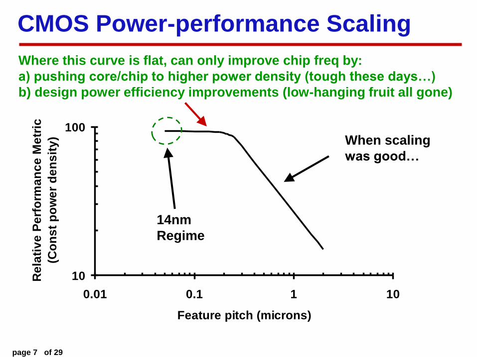
CMOS Power-performance Scaling
Where this curve is flat, can only improve chip freq by:
a) pushing core/chip to higher power density (tough these days…)
b) design power efficiency improvements (low-hanging fruit all gone)
14nm
Regime
When scaling
was good…
page 8 of 29
From IEEE ISSCC 2013 Supplement:
page 9 of 29
Lithography Scaling
0.1
1
0.01 0.1 1
Feature pitch (microns)
Ra
yle
igh
Fa
cto
r (k
1) Conventional lithography
Double patterning
14nm
Regime
k1 = (resolution)*NA
l
OPC, OAI,
Computational
Lithography
page 10 of 29
Outline
Introduction
Classical CMOS Scaling: The End of the Road
New Device Structures
What do these structures mean for circuit designers?
Wire Interconnects
Reliability
Conclusions
page 11 of 29
Multigate/FinFET Devices
G
S
D
FinFET dual-gate cross section
Gate Electrode
FinFET dual-gate cross section
Gate ElectrodeGate Electrode
FinFET tri-gate cross section
Gate Electrode
FinFET tri-gate cross section
Gate ElectrodeGate Electrode
page 12 of 29
Trigate/FinFET Devices
The good news:
Expect improved subthreshold slope
Expect improved RDF-induced variability
Above could help to enable lower voltage operation
What designers have to worry about:
New sources of variability Fin width will have a significant impact on VT: Expect global, local
and random effects/correlations Fin height -> width variability: can’t amortize over wider fingers…
Some of the same old variability issues (continuing to worsen…) Gate line-edge roughening (LER), channel length variability May be exacerbated by 3D effects
“Quantization” of device widths Can only have integer numbers of fins
Changes in device parasitic R, C compared to usual expectations G-S cap (Miller cap), S, D contact resistance
page 13 of 29
0
50
100
s[V
Ts
at], m
V
1/√ (number of fins)
nFET
pFET1 fin
20,10,5 fins2 fins
Trigate/FinFET Devices: Variability
Reduced RDF-relatedVT variability for FINFETs
(~25-50% depending on design)
eg. M. Jurczak et al,
Proc. 2009 IEEE Int, SOI Conf.
LER-relatedVT variability for FINFETs
eg. E. Baravelli et al, IEEE T. Nanotechnol. 7, p. 291 (2008).
Warning: considerable spread in reported literature: your mileage may vary
0
10
20
30
40
0 5 10
Planar
Bulk FinFET
SOI FinFET
s[V
T], m
V
0 5 101/√ (WL) (mm-1)
page 14 of 29
0
0.2
0.4
0.6
0.8
1
0 1 2 3 4 5 6 7 8 9
Device Width (Units of Min width device)
finFET Devices Conventional Devices
Trigate/FinFET Devices: Quantization
Example: min size finFET INV
Can have p:n ratio = 1, 0.5, 2(nothing in between)
Also, even a “wide” device willalways be just a collectionof very narrow devices…
Plus, expect difficulty to createmultiple VT offerings in a fully depleted device scenario
De
vic
e S
tre
ng
th (
arb
Un
its)
Higher VT(less leakage)
Lower VT(more perf.)
Device Width (ratio to min width device)
• Likely to create most difficulty for SRAM, register file designs
• Also small feedback devices, keepers, etc.
• Issue for any device tuner, other tools expecting continuous width ranges
page 15 of 29
• Resistance in contacts to fins might be tricky: assume it can be handled by device engineers! What about G-S cap?
Trigate/FinFET Devices: Parasitics
G
S
D
D SG
• Expect increase in Cgs comparedto planar structures
• Details will depend on fin vs trigate, fin pitch, height, thickness, etc.
• Might have to watch out for certaintypes of noise issues
• Might decrease static timing accuracy
page 16 of 29
• Sea-of-fins technology is attractive: offers tightest fin pitch
• Additional constraint on PD cell image
• Vertical: Fin, metal pitches Horizontal: gate, metal pitches
Trigate/FinFET Devices: PD Issues
Meta
l Pitc
h
Fin
Pitc
h
Metal Pitch
Gate Pitch
Example:12:16
page 17 of 29
FinFET PD Implications
Higher fins -> more current drive per unit area
But technology minimum device width grows
Quantization issues tougher to deal with
Finer fin pitch -> more current drive per unit area
Can trade off shorter fin height with finer fin pitch
Sea-of-fins constraints, other litho-related constraints
Net: stronger technology <-> PD interaction
Library cell definition likely to be dependent on technology fin pitch
Will need to find gear ratios (metal pitch vs fin pitch) that work well together
page 18 of 29
Outline
Introduction
Classical CMOS Scaling: The End of the Road
New Device Structures
What do these structures mean for circuit designers?
Wire Interconnects
Reliability
Conclusions
page 19 of 29
Wire Interconnect Scaling (or lack thereof…)
Assume all logic scales with litho shrink factor
Wire lengths then also would scale
Best case scenario: RC stays constant (“perfect scaling”) This is already painful, chip area generally hasn’t been shrinking!
Data below shows expectations that wire delays will grow significantly, even in scaled designs.