Joseph A. Elias, PhD 1 Class 01: Overview of IC Design Flow Topics: 1. Introduction 2. Moore’s Law 3. Chip Process Flow 4. DPW: Motivation for Increasing Wafer Diameter 5. Chip Design Flow 6. Logic, Circuit, Models 7. Simulation 8. Layout Verification and Delay Extraction 9. Masks 10. Tests
Transcript
Joseph A. Elias, PhD1
Class 01: Overview of IC Design Flow
Topics:1. Introduction2. Moore’s Law3. Chip Process Flow4. DPW: Motivation for Increasing Wafer Diameter5. Chip Design Flow6. Logic, Circuit, Models7. Simulation8. Layout Verification and Delay Extraction9. Masks10. Tests
Joseph A. Elias, PhD2
Class 01: Overview of IC Design Flow
In 1965, Gordon Moore was preparing a speech and made a memorable observation. When he started to graph data about thegrowth in memory chip performance, he realized there was a striking trend. Each new chip contained roughly twice as muchcapacity as its predecessor, and each chip was released within 18-24 months of the previous chip. If this trend continued, hereasoned, computing power would rise exponentially over relatively brief periods of time.
Moore's observation, now known as Moore's Law, described a trend that has continued and is still remarkably accurate. It is thebasis for many planners' performance forecasts. In 26 years the number of transistors on a chip has increased more than 3,200times, from 2,300 on the 4004 in 1971 to 7.5 million on the Pentium¨ II processor.
10um 1um 0.35um
Moore’s Law (http://www.intel.com/intel/museum/25anniv/hof/moore.htm)
Feature Size,aka Process Node
Joseph A. Elias, PhD3
Class 01: Overview of IC Design FlowChip Process Flow (Wolf p.3)
Feature Size
200mm-300mm
0.6um
Joseph A. Elias, PhD4
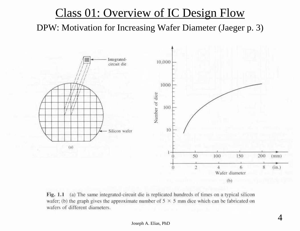
Class 01: Overview of IC Design FlowDPW: Motivation for Increasing Wafer Diameter (Jaeger p. 3)
Joseph A. Elias, PhD5
Class 01: Overview of IC Design FlowChip Design Flow (Wolf p.2)
Joseph A. Elias, PhD6
Class 01: Overview of IC Design FlowLogic, Circuit, Models (Martin ch. 1)
Joseph A. Elias, PhD7
Class 01: Overview of IC Design FlowSimulation (Martin ch. 1)
Analog Simulation - HSPICE, et.al.Digital (Logic) Simulation - Verilog, et.al.
Joseph A. Elias, PhD8
Class 01: Overview of IC Design FlowLayout Verification and Extraction (Martin p.55)
Extraction - determining device and parasitic information
Joseph A. Elias, PhD9
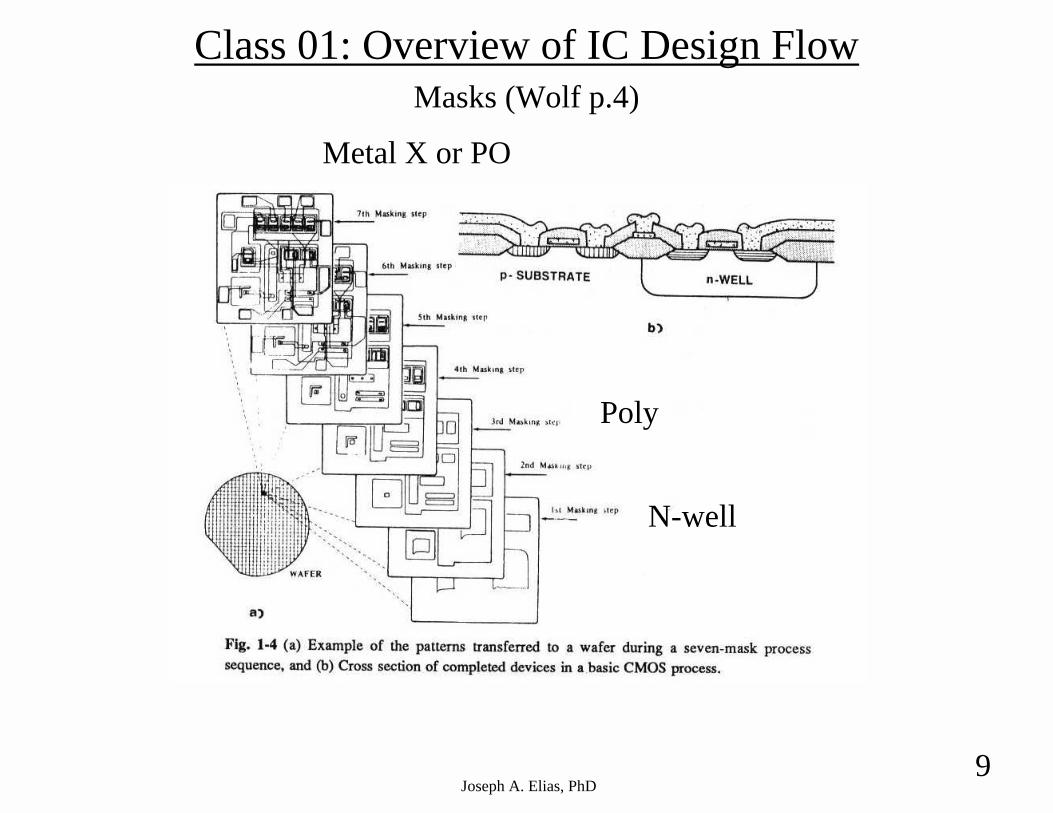
Class 01: Overview of IC Design FlowMasks (Wolf p.4)
N-well
Metal X or PO
Poly
Joseph A. Elias, PhD10
Class 01: Overview of IC Design FlowTesting (from experience)