119 PHYSICS Time allowed : 3 hours Maximum marks: 70 General Instructions: (i) All questions are compulsory. (ii) There is no overall choice. However, an internal choice has been provided in one question of two marks, one question of three marks and all three questions of five marks. You have to attempt only one of the choice in such questions. (iii) Question numbers 1 to 5 are very short answer type questions, carrying one mark each. (iv) Question numbers 6 to 12 are short answer type questions, carrying two marks each. (v) Question numbers 13 to 24 are also short answer type questions, carrying three marks each. (vi) Questions numbers 25 to 27 are long answer type questions, carrying five marks each. (vii) Use of calculators is not permitted. However, you may use log tables, if necessary. (viii) You may use the following values of physical constants wherever necessary: Mass of neutron Boltzmann's constant Avogadro's number QUESTION PAPER CODE 55/1/1 1. An electron, an alpha-particle and a proton have the same kinetic energy. Which one of these particles has the largest de-Broglie wavelength ? 1 2. Why should the material used for making permanent magnets have high coercivity ? 1
Transcript
119
PHYSICS
Time allowed : 3 hours Maximum marks: 70
General Instructions:
(i) All questions are compulsory.
(ii) There is no overall choice. However, an internal choice has been provided in onequestion of two marks, one question of three marks and all three questions of fivemarks. You have to attempt only one of the choice in such questions.
(iii) Question numbers 1 to 5 are very short answer type questions, carrying one markeach.
(iv) Question numbers 6 to 12 are short answer type questions, carrying two markseach.
(v) Question numbers 13 to 24 are also short answer type questions, carrying threemarks each.
(vi) Questions numbers 25 to 27 are long answer type questions, carrying five markseach.
(vii) Use of calculators is not permitted. However, you may use log tables, if necessary.
(viii) You may use the following values of physical constants wherever necessary:
Mass of neutron
Boltzmann's constant
Avogadro's number
QUESTION PAPER CODE 55/1/1
1. An electron, an alpha-particle and a proton have the same kinetic energy. Which
one of these particles has the largest de-Broglie wavelength ? 1
2. Why should the material used for making permanent magnets have highcoercivity ? 1
120
3. The radioactive isotope D decays according to the sequence
If the mass number and atomic number of D1 are 176 and 71 respectively, what
is (i) the mass number (ii) atomic number of D ? 1
4. What will be the values of input A and B for the Boolean expression
1
5. Why is frequency modulation perferred over amplitude modulation fortransmission of music ? 1
6. The output of an OR gate is connected to both the inputs of a NAND gate. Draw
the logic circuit of this combination of getes and write its truth table. 2
7. Draw a plot of potential energy of a pair of nucleons as a function of their separation.
What is the significance of negative potential energy in the graph drawn ? 2
8. A convex lens of refractive index 1.5 has a focal length of 18 cm in air. Calculate
the change in its focal length when it is immersed in water of refractive index 2
9. Distinguish between the terms 'average value' and 'rms value' of an alternating
current. The instantaneous current from an a.c. source is I = 5 sin (314 t) ampere.
What are the average and rms values of the current ? 2
10. Write the relation for the forece acting on a charge carrier q moving with avelocity through a magnetic field in vector notation. Using this relation,
deduce the conditions under which this force will be (i) maximum (ii) minimum. 2
11. A cylindrical metallic wire is stretched to increase its length by 5%. Calculate the
percentage change in its resistance. 2
12. The electric field E due to a point charge at any point near it is defined as
where q is the test charge and F is the force acting on it. What is the physicalsignificance of in this expression ? Draw the electric field lines of a point
charge Q when (i) Q>0 and (ii) Q<0. 2
OR
Define electric flux. Write its S.I. units. A spherical rubber balloon carries a chargethat is uniformly distributed over its surface. As the balloon is blown up and increasesin size, how does the total electric flux coming out of the surface change ? Givereason.
121
13. Deduce an expression for the electric potential due to an electric dipole at anypoint on its axis. Mention one contrasting feature of electric potential of a dipole ata point as compared to that due to a single charge. 3
14. A parallel plate capacitor, each with plate area A and separation d, is charged to apotential difference V. The battery used to charge it is then disconnected. A dielectricslab of thickness d and dielectric constant K is now placed between the plates.What change, if any, will take place in(i) charge on the plates(ii) electric field intensity between the plates(iii) capacitance of the capacitor.
Justify your answer in each case. 3
15. State Kirchhoff's rules of current distribution in an electrical network.Using these rules determine the value of the current I
1 in the electric circuit given
below. 3
16. Write the mathematical relation for the resistivity of a material in terms ofrelaxation time, number density and mass and charge of charge carriers in it.Explain, using this relation, why the resistivity of a metal increases and that ofa semi-conductor decreases with rise in temperature. 3
17. Explain with the help of a labelled diagram the underlying principle and workingof a step-up transformer. Why cannot such a device be used to step-up d.c.voltage ? 3
ORDraw a labelled diagram of an a.c. generator. Explain briefly its principle andworking. 3
18. Given below are two electric circuits A and B
Calculate the ratio of power factor of the circuit B to the power factor ofcircuit A. 3
122
19. Define the term 'resolving power' of an astronomical telescope. How does it getaffected on(i) increasing the aperture of the objective lens ?
(ii) increasing the wavelength of the light used ?
Justify your answer in each case. 3
20. Write any four characteristics of electromagnetic waves. Give two uses each of(i) Radio-waves (ii) Micro-waves. 3
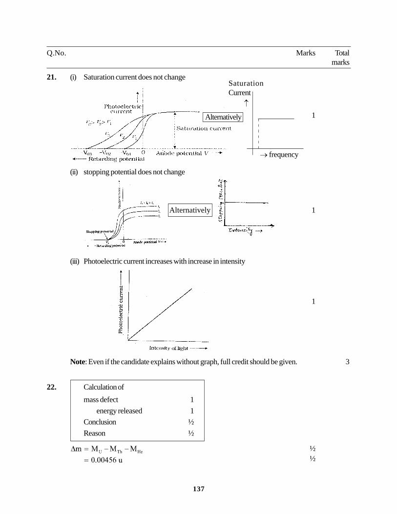
21. In a plot of photoelectric current versus anode potential, how does
(i) the saturation current vary with anode potential for incident radiations ofdifferent frequencies but same intensity ?
(ii) the stopping potential vary for incident radiations of different intensities butsame frequency ?
(iii) photoelectric current vary for different intensities but same frequency ofincident radiations ?
Justify your answer in each case. 3
22. Calculate the amount of energy released during the of
Given : 1. atomic mass of
2. atomic mass of
3. atomic mass of
Is this decay spontaneous ? Give reason. 3
23. What is a digital signal ? Explain the function of modem in data communication.Write two advantages of digital communication. 3
24. Explain, with the help of a schematic diagram, the principle and working of aLight Emitting Diode. What criterion is kept in mind while choosing the semi-conductor material for such a device ? Write any two advantages of LightEmitting Diode over conventional incandescent lamps. 3
25. Draw a labelled diagram of a moving coil galvanometer. State the principle onwhich it works.
Deduce an expression for the torque acting on a rectangular current carrying loopkept in a uniform magnetic field. Write two factors on which the current sensitivityof a moving coil galvanometer depend. 5
OR
123
State Biot-Savart law. Use it to derive an expression for the magnetic field at thecentre of a circular loop of radius R carrying a steady current I. Sketch the magnetic
field lines for such a current carrying loop. 5
26. What are coherent sources ? Why are coherent sources required to produceinterference of light ? Give an example of interference of light in everyday life.
In Young's double slit experiment, the two slits are 0.03 cm apart and the screen isplaced at a distance of 1.5 m away from the slits. The distance between the centralbright fringe and fourth bright fringe is 1 cm. Calculate the wavelength of lightused. 5
OR
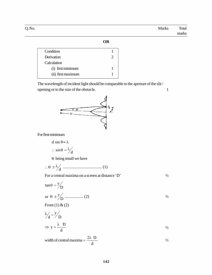
State the condition under which the phenomenon of diffraction of light takes place.
Derive an expression for the width of the central maximum due to diffraction oflight at a single slit.
A slit of width 'a' is illuminated by a monochromatic light of wavelength 700 nm atnormal incidence. Calculate the value of 'a' for position of
(i) first minimum at an angle of diffraction of 30°.
(ii) first maximum at an angle of diffraction of 30°. 5
27. State the principle of working of p-n diode as a rectifier. Explain, with the help ofa circuit diagram, the use of p-n diode as a full wave rectifier. Draw a sketch of the
input and output waveforms. 5
OR
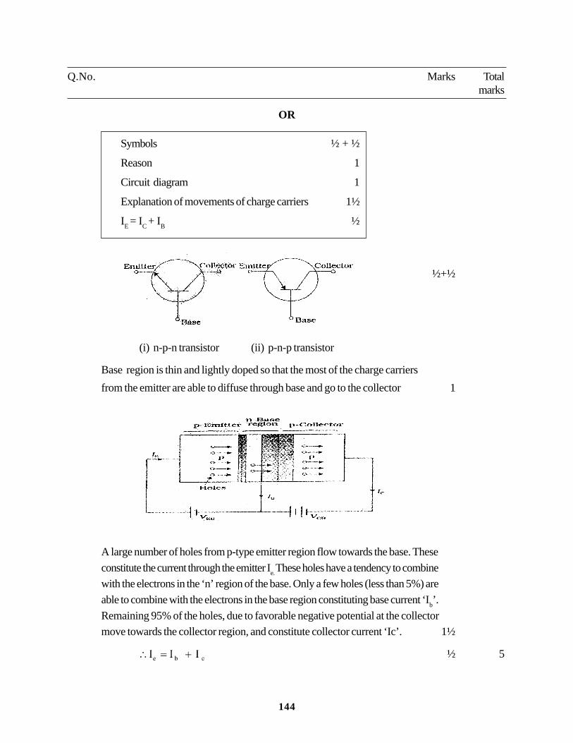
Draw the symbolic representation of a (i) p-n-p, (ii) n-p-n transistor. Why is thebase region of transistor thin and lightly doped ? With proper circuit diagram,show the biasing of a p-n-p transistor in common base configuration. Explain themovement of charge carriers through different parts of the transistor in such aconfiguration and show that 5
QUESTION PAPER CODE 55/1
1. In a series LCR circuit, the voltages across an inductor, a capacitor and a resistorare 30 V, 30 V and 60 V respectively. What is the phase difference between theapplied voltage and the current in the circuit ? 1
2. Ultraviolet radiations of different frequencies and are incident on twophotosensitive materials having work functions W
1 and W
2 (W
1>W
2)
respectively. The kinetic energy of the emitt3ed electrons is same in both the cases.
Which one of the two radiations will be of higher frequency ? 1
124
3. Define the term 'activity' of radionuclide. Write its SI unit. 1
4. An electron is moving a along +ve x-axis in the presence of uniform magnetic field
along +ve y-axis. What is the direction of the force acting on it ? 1
5. What should be the length of dipole antenna for a carrier wave of frequency
6×10⁸ Hz ? 1
6. Two point charges and are separated by a distance of 1 m in air.Calculate at what point on the line joining the two charges is the electric potentialzero. 2
7. A voltage of 30 V is applied across a carbon resistor with first, second and thirdrings of blue, black and yellow colours respectively. Calculate the value of current,in mA, through the resistor. 2
8. A galvanometer has a resistance of 30Ω. It gives full scale deflection with acurrent of 2 mA. Calculate the value of the resistance needed to convert it into anammeter of range 0-0.3 A. 2
9. Calculate the current drawn by the primary of a transformer which steps down200 V to 20 V to operate a device of resistance 20Ω. Assume the efficiency ofthe transformer to be 80%. 2
ORAn a.c. voltage of 100 V, 50 Hz is connected across a 20 ohm resistor and mHinductor in series. Calculate (i) impedance of the circuit, (ii) rms current in thecircuit.
10. Define resolving power of a compound microscope. How does the resolvingpower of a compound microscope change when
(i) refractive index of the medium between the object and objective lensincreases ?
(ii) wavelength of the radiation used is increased ? 2
11. Draw a graph showing the variation of potential energy between a pair of nucleonsas a function of their separation. Indicate the regions in which the nuclear force is(i) attractive, (ii) repulsive. 2
12. Two semiconductor materials X and Y shown in the given figure, are made bydoping germanium crystal with indum and arsenic respectively. The two are joinedend to end and connected to a battery as shown.
125
(i) Will the junction be forward biased or reverse biased ?
(ii) Sketch a V-I graph for this arrangement. 2
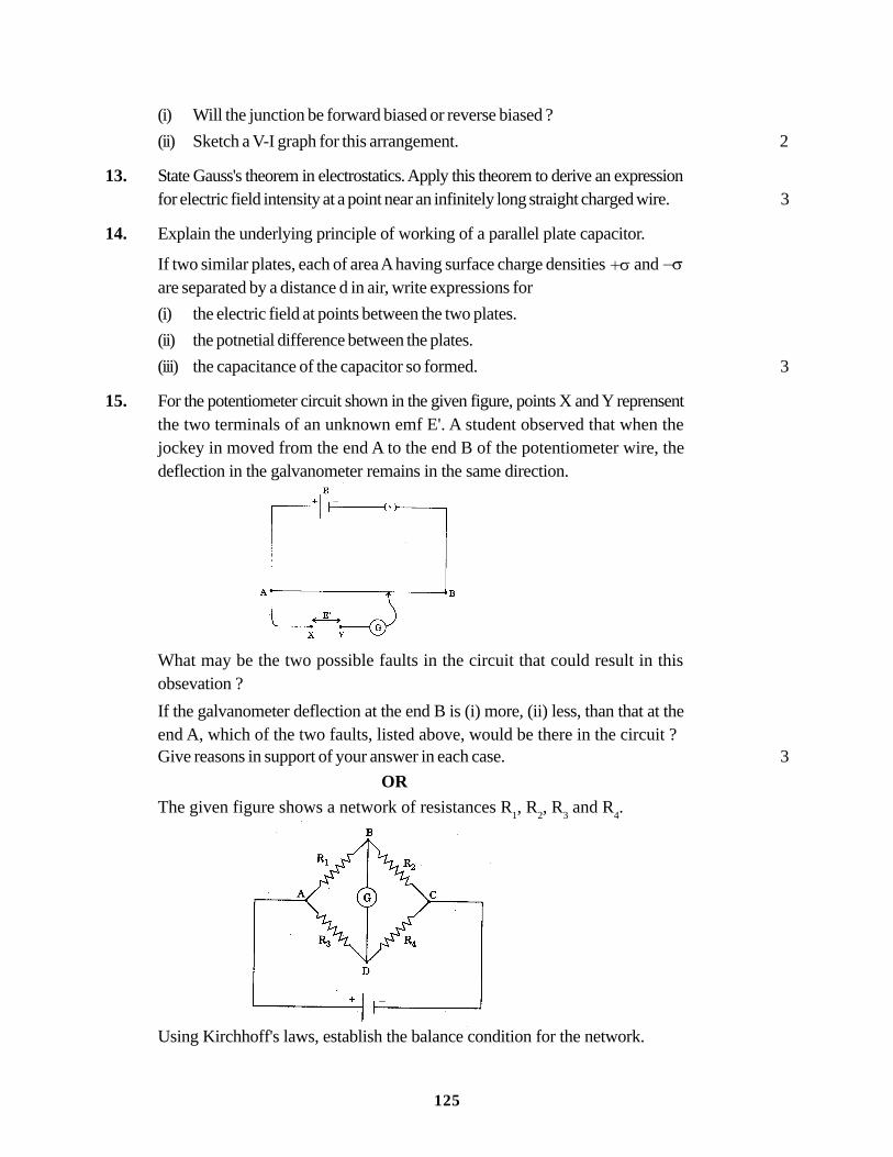
13. State Gauss's theorem in electrostatics. Apply this theorem to derive an expressionfor electric field intensity at a point near an infinitely long straight charged wire. 3
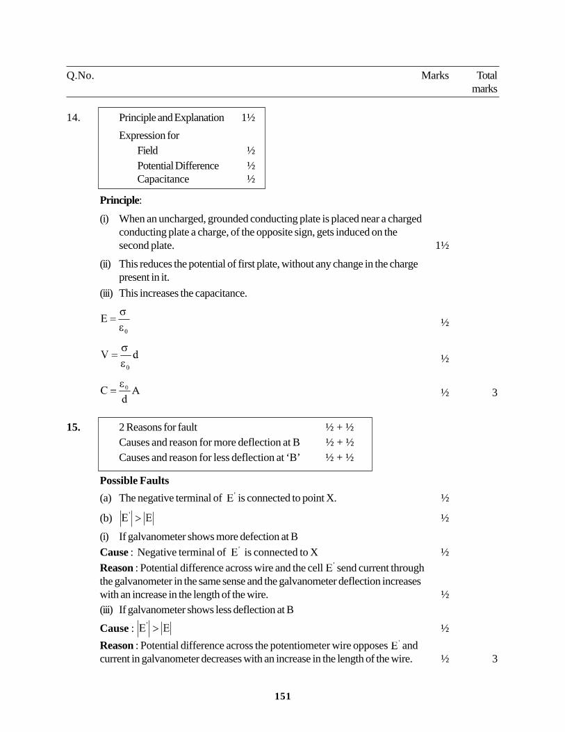
14. Explain the underlying principle of working of a parallel plate capacitor.
If two similar plates, each of area A having surface charge densities and are separated by a distance d in air, write expressions for
(i) the electric field at points between the two plates.
(ii) the potnetial difference between the plates.
(iii) the capacitance of the capacitor so formed. 3
15. For the potentiometer circuit shown in the given figure, points X and Y reprensentthe two terminals of an unknown emf E'. A student observed that when thejockey in moved from the end A to the end B of the potentiometer wire, thedeflection in the galvanometer remains in the same direction.
What may be the two possible faults in the circuit that could result in thisobsevation ?
If the galvanometer deflection at the end B is (i) more, (ii) less, than that at theend A, which of the two faults, listed above, would be there in the circuit ?Give reasons in support of your answer in each case. 3
OR
The given figure shows a network of resistances R1, R
2, R
3 and R
4.
Using Kirchhoff's laws, establish the balance condition for the network.
126
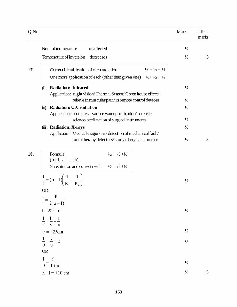
16. What is Seebeck effect ? Plot a graph showing the variation of thermo emf withtemperature of hot junction (keeping cold junction at 0°C) of a thermocouple.How will the (i) neutral temperature, (ii) inversion temperature of a thermocouplechange when the temperature of cold junction is increased ? 3
17. Name the following constituent radiations of electromagnetic spectrum which(i) produce intense heating effect.
(ii) is absorbed by the ozone layer in the atmosphere.
(iii) is used for studying crystal structure.
Write one more application forr each of these radiations. 3
18. A double convex lens of glass of refractive index 1.6 has its both surfaces ofequal radii of curvature of 30 cm each. An object of height 5 cm is placed ata distance of 12.5 cm from the lens. Calculate the size of the image formed. 3
19. Draw a schematic diagram of the experimental arrangement used by Davissonand Germer to establish the wave nature of electrons. Explain briefly how thede-Broglie relation was experimentally verified in case of electrons. 3
20. Draw the graph to show variation of binding energy per nucleon with mass
number of different atomic nuclei. Calculate binding energy/nucleon of nucleus. 3
Given :mass of
mass of proton = 1.007825 umass of neutron = 1.008665 uand 1 u = 931 MeV/C2
21. Draw the circuit diagram of a common emitter amplifier using n-p-n transistor.What is the phase differnece between the input signal and output voltage ? Statetwo reasons why a common emitter amplifier is preferred to a common baseamplifier. 3
22. Explain the formation of energy band in solids. Draw energy band diagram for(i) a conductor, (ii) an intrinsic semiconductor. 3
23. What is modulation ? Explain the need of modulating a low frequency informationsignal. With the help of diagrams, differentiate between PAM and PDM. 3
24. Write the acronym LASER in expanded form. State any four reasons for preferringdiode lasers as light sources for optical communication links. 3
25. Explain, with the help of a labelled diagram, the principle and construction of acyclotron.
Deduce an expression for the cyclotron frequency and show that it does not dependon the speed of the charged particle. 5
127
OR
Distinguish the magnetic properties of dia, para- and ferro-magnetic substances in
terms of (i) susceptibility, (ii) magnetic permeability and (iii) coercivity. Give one
example of each of these materials.
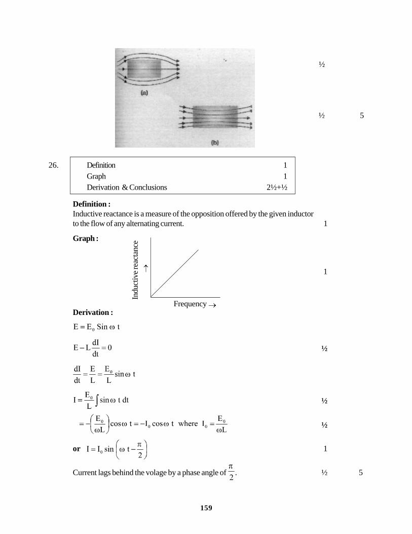
Draw the field lines due to an external magnetic field near a (i) diamagnetic,
(ii) paramagnetic substance.
26. Explain the term 'inductive reactance'. Show graphically the variation of inductive
reactance with frequency of the applied alternating voltage.
An a.c. voltage is applied across a pure inductor of inductance L.
Show mathematically that the current flowing through it lags behind the applied
voltage by aphase angle of π/2. 5
OR
Explain the term 'capacitive reactance'. Show graphically the variation of capacitive
reactance with frequency of the applied alternating voltage.
An a.c. voltage is applied across a pure capacitor of capacitance
C. Show mathematically that the current flowing through it leads the applied voltage
by a phase angle of π/2.
27. State the essential condition for diffraction of light to take place.
Use Huygen's principle to explain diffraction of light due to a narrow single slit and
the formation of a patern of fringes obtained on the screen. Sketch the pattern of
fringes formed due to diffraction at a single slit showing variation of intensity with
angle 5
OR
What are coherent sources of light ? Why are coherent sources required to obtain
sustained interference pattern ?
State three characteristic features which distinguish the interference pattern due to
two coherently illuminated sources as compared to that observed in a diffraction
pattern due to a single slit.
128
Marking Scheme — Physics
General Instructions :
1. The Marking Scheme provides general guidelines to reduce subjectivity in the marking.
The answers given in the marking scheme are suggested answers. The content is thus
indicative. If a student has given any other answer, which is different from the one given
in the Marking Scheme, but conveys the meaning correctly, such answers should be given
full weightage.
2. Evaluation is to be done as per instructions provided in the marking scheme. It should
not be done according to one’s own interpretation or any other consideration. Marking
Scheme should be strictly adhered to and religiously followed.
3. If a question has parts, please award marks in the right hand side for each part. Marks
awarded for different part of the question should then be totalled up and written in the
left hand margin and circled.
4. If a question does not have any parts, marks are be awarded in the left hand margin only.
5. If a candidate has attempted an extra question, marks obtained in the question attempted
first should be retained and the other answer should be scored out.
6. No marks to be deducted for the cumulative effect of an error. The student should be
penalized only once.
7. Deduct ½ marks for writing wrong units, or missing units, in all numerical problems.
8. Formula can be taken as implied from the calculations even if not explicitly written.
9. In short answer type questions, asking for two features/ characteristics/ properties, if a
candidate writes three features/ characteristics/ properties or more, only the first two
should be evaluated.
10. Full marks should be awarded to a candidate if his/her answer in a numerical problem
is close to the value given in this scheme.
11. Award full marks to the answer of a questions if it deserves.
129
QUESTION PAPER CODE 55/1/1
EXPECTED ANSWERS/VALUE POINTS
Q.No. Marks Totalmarks
1. Electron 1 1
2. Magnetisation is not easily erased by stray magnetic field/ minor mechanicaldamage/ temperature variation 1 1
3. (i) Mass number 180 ½
(ii) Atomic number 72 ½
OR
1
4. A = 0 ½B = 0 ½ 1
5. Better quality transmission/ larger band width/ Atmospheric or man madeelectrical noise signal do little harm. 1 1
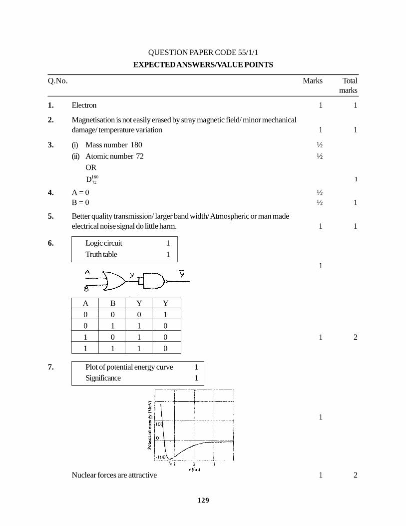
6. Logic circuit 1
Truth table 1
1
A B Y Y
0 0 0 1
0 1 1 0
1 0 1 0 1 2
1 1 1 0
7. Plot of potential energy curve 1Significance 1
1
Nuclear forces are attractive 1 2
130
Q.No. Marks Totalmarks
8. Formula ½
Calculation 1
Result ½
½
for air
½
for water
½
Change in focal length = 3fa = 54 cm ½ 2
9. Average value ½
rms value ½
Calculation of AV value ½
Calculation of rms value ½
Average value of an alternating current over a time T is
½
rms value of an alternating current is that value of steady current which when
flowing through a resistance for a certain amount of time produces same amount
of heat as the given A.C. does in the same resistance in the same time. ½
Average value over half cycle is
or Average value over complete cycle is zero ½
rms value is or ½ 2
131
10. Expression 1
Condition of maximum ½
Condition of minimum ½
1
(i) Maximum when
½
(ii) Minimum when
or 180° ½ 2
11. Formula ½
Calculation 1
Result ½
½
1
½
(full credit to be given even if % change is given approximately as 10%) 2
12. Significance 1
Field pattern for (i) ½
Field pattern for (ii) ½
We say so to ensure that the source charge remains (almost) undisturbed in the presence
of the test charge. 1
Q.No. Marks Totalmarks
132
½
½ 2
OR
Definition ½
Unit ½
Effect on flux ½
Reason ½
Electric flux is the total number of electric field lines passing normally througha given surface.
OR Electric Flux = ½
S.I. unit Nm2/C OR V.m ½
No Change ½As the total charge enclosed remains the same. ½ 2
13. Derivation 2
Contrasting feature 1
½
Q.No. Marks Totalmarks
-q +q P
x2a
133
Potential at P due to +q
½
Potential at P due to -q
½
potential at P due to the dipole
for a<<x , we have
½
For a single charge V ½
For a dipole V ½ 3
14. (i) Effect on charge with justification ½ + ½
(ii) Electric field with justification ½ + ½
(iii) Capacitance with justification ½ + ½
(i) No change ½As the battery is disconnected ½
(ii) Decreases OR becomes times ½
Due to polarization of the dielectric ½
(iii) Increases OR becomes k times ½ As the electric field, and therefore, the p.d., between the plates decreases ½ 3
15. Statement ½ + ½
Calculation of I1
2
Junction Rule : At any junction of several circuit elements the sum of currents
entering the junction must be equal to the sum of currents leaving it. ½
Loop Rule : Algebraic sum of changes in the potential around any closed loopmust be zero. ½
Q.No. Marks Totalmarks
134
Loop ABCFA
I1
+ 2I3 = 2 ............................... (1) ½
Loop FCDEF
2I3
+ I2 = 6 ................................ (2) ½
At F, I1 + I
2 = I
3 .......................... (3) ½
Solving (1), (2) and (3)
I1 = _ 0.8 A ½ 3
16. Relation 1
Explanation 1 + 1
1
For a metal, as the temperature increases, decreases. Hence increases. 1For a semiconductor, as the temperature increases, number density of electrons inthe conduction band increases. Hence decreases. 1 3
17. Labelled diagram 1Principle ½Working 1Reason ½
1
Q.No. Marks Totalmarks
I2
F
135
Principle : When alternating current flows through the primary, the magnetic fluxlinked with the secondary changes. As a result, an e.m.f. is induced in it.
ORIt works on the principle of Mutual Induction. ½Working : 1Change of flux is zero for d.c. ½
OR
Diagram 1
Principle 1
Working 1
1
Alternatively
Principle:-It works on the principle of electromagnetic induction. 1 OR
When a coil is rotated in a magnetic field, magnetic flux linked with it changes.Hence an emf is induced in it.
Working: 1 3
18. Formula 1
Calculation 2
½
½
1
1 3
Q.No. Marks Totalmarks
136
19. Definition 1
Affect of
(i) Aperture ½
(ii) Wavelength ½
Justification i) ½
ii) ½
Resolving power (R.P) is the reciprocal of limit of angular resolution 1OR any other suitable definition.
(i) Increases ½
Resolving power = ½
R.P is directly proportional to ‘d’ (For a given ) ½
(ii) Decreases R.P is inversely proportional to '' (For a given d ) ½ 3
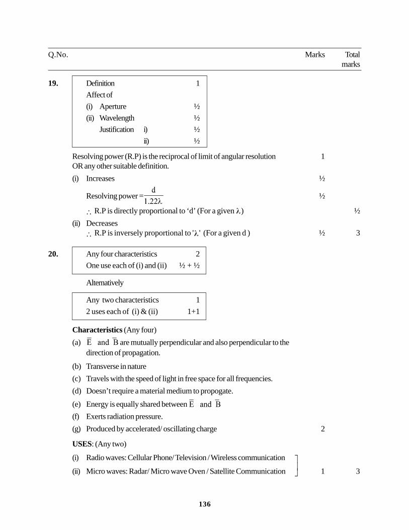
20. Any four characteristics 2
One use each of (i) and (ii) ½ + ½
Alternatively
Any two characteristics 1
2 uses each of (i) & (ii) 1+1
Characteristics (Any four)
(a) are mutually perpendicular and also perpendicular to thedirection of propagation.
(b) Transverse in nature
(c) Travels with the speed of light in free space for all frequencies.
(d) Doesn’t require a material medium to propogate.
(e) Energy is equally shared between
(f) Exerts radiation pressure.
(g) Produced by accelerated/ oscillating charge 2
USES: (Any two)
(i) Radio waves: Cellular Phone/ Television / Wireless communication
(ii) Micro waves: Radar/ Micro wave Oven / Satellite Communication 1 3
Q.No. Marks Totalmarks
137
21. (i) Saturation current does not change
1
(ii) stopping potential does not change
Alternatively 1
(iii) Photoelectric current increases with increase in intensity
1
Note: Even if the candidate explains without graph, full credit should be given. 3
22. Calculation of
mass defect 1
energy released 1
Conclusion ½
Reason ½
½½
Q.No. Marks Totalmarks
Alternatively
frequency
SaturationCurrent
138
½
= 0.00456 × 931.5
= 4.25 MeV ½Yes ½As m is positive. ½ 3
23. Meaning 1
Function of Modem 1
Advantages ½ + ½
A digital signal is one which can have only two discrete values 1
Modem converts digital data to analog at the transmitting end and convertsanalog to digital at the receiver end.
OR
It modulates and demodulates in digital communication 1
Advantage:
(a) It is much easier for receiver to detect pulses.
(b) Error and noise free communication
(c) Large number of signals can be sent through a single channel
(d) Data rate is faster
(Any two) ½+½ 3
24. Diagram ½
Principle ½
Working ½
Criterion ½
Advantages ½ + ½
1
Q.No. Marks Totalmarks
139
Principle:
When electrons fall from a higher to a lower energy level, containing holes, ½
energy, in the form of light radiation, gets released.
Working : ½
Criterion :
The semiconductor material used in LED is chosen according to the required
wavelength of emitted radiation ½
OR
Chosen to have a energy gap matching the energy of a photon of the radiation
required to be emitted.
Advantages:
(a) Low operation voltage
(b) Less power
(c) No warm up time
(d) Fast action
(e) Light emitted is nearly monochromatic
(f) Long life
(Any two) ½+½ 3
25. Labelled Diagram 1
Principle 1
Derivation of expression of torque 2
Two Factors ½ + ½
1
Q.No. Marks Totalmarks
140
Principle : When a current carrying coil is kept in a uniform magnetic field itexperiences a torque. 1
Derivation :
(M = NIA)
OR2
Current sensitivity depends on(a) number of turns(b) strength of the magnetic field(c) torsional constant of the suspension wire(d) Area of the coil(Any two) ½+½ 5
OR
Statement 1
Derivation 2
magnetic Field Lines 2
Statement : The magnitude of the magnetic field, dB, at any point, due to acurrent carrying conductor, is directly propertional to the current, I, the elementlength 'd1' and inversely proportional to the square of the distance 'r'. Its direction
is perpendicular to the plane containing 'dl' and r as defined by . 1
½
½
Q.No. Marks Totalmarks
Derivation
141
1
½
(also accept the direct derivation of the field at the centre of the coil)
1 5
26. Meaning 1
Need 1
Example ½
Formula 1
Calculation 1
Result ½
Two sources are said to be coherent when they produce light, of samewavelength, in phase, or with a constant phase difference, continuously. 1
If the sources are not coherent the average intensity at any given point willbe same and interference pattern would not be observable. 1
Colours in a soap bubble / colours seen on a thin oil film on water. ½
1
1
` ½ 5
Q.No. Marks Totalmarks
142
OR
Condition 1Derivation 2Calculation
(i) first minimum 1(ii) first maximum 1
The wavelength of incident light should be comparable to the aperture of the slit /opening or to the size of the obstacle. 1
For first minimum
being small we have
..................................... (1)
For a central maxima on a screen at distance ‘D’ ½
.................. (2) ½
From (1) & (2)
½
width of central maxima ½
Q.No. Marks Totalmarks
143
(i)
½
½
(ii)
½
½ 5
27. Principle 1
Circuit Diagram 2
Explanation 1
Sketch ½ + ½
Principle : p-n function diode conducts when it is forward biased and doesn’tconduct when it is reverse biased 1
Explanation: 1Wave form:
½
½ 5
(Full marks will be awarded if input and output wave form are shown with thecircuit diagram.)
Q.No. Marks Totalmarks
144
OR
Symbols ½ + ½
Reason 1
Circuit diagram 1
Explanation of movements of charge carriers 1½
IE = I
C + I
B½
½+½
(i) n-p-n transistor (ii) p-n-p transistor
Base region is thin and lightly doped so that the most of the charge carriers
from the emitter are able to diffuse through base and go to the collector 1
A large number of holes from p-type emitter region flow towards the base. These
constitute the current through the emitter Ie. These holes have a tendency to combine
with the electrons in the ‘n’ region of the base. Only a few holes (less than 5%) are
able to combine with the electrons in the base region constituting base current ‘Ib’.
Remaining 95% of the holes, due to favorable negative potential at the collector
move towards the collector region, and constitute collector current ‘Ic’. 1½
½ 5
Q.No. Marks Totalmarks
145
QUESTION PAPER CODE 55/1
EXPECTED ANSWERS/VALUE POINTS
Q.No. Marks Totalmarks
1. Applied Voltage and current are in the same phase
OR
1 1
2. 1 1
3. Definition ½
Unit ½
The total decay rate of a sample of one or more radionuclide is called activityOR
Radioactive disintegration taking place per second. OR
R= , where N is the total number of radionuclides at any time ‘t’. ½
SI unit-becquerel(Bq) ½ 1
4. along –ve z axis OR 1 ½
(Even if the student writes perpendicular to the direction of motion award full marks)
5. Calculation of ½
Length of antenna ½
(i) ½
(ii)
146
OR
½ 1
(award full mark even if the student writes the answer directly)
6. Formula ½
Substitution ½
Calculation ½
Result ½
When point is taken on the line between the two charges
½
1
Substitution & calculation,
x = 1/3 m (from -2 ) ½
Or 0.33 m
Alternatively: If point is taken on the extended line, beyond -2.
½
1
Calculation,
y = 1 m (from -2 ) ½ 2
7. Calculation of R 1
(using colour code)
Calculation of I ½
Expressing I in mA ½
Q.No. Marks Totalmarks
147
Q.No. Marks Totalmarks
Calculation of ‘R’ = 60 × 104 Ω 1
Calculation of I ; ½
In mA, I = 0.05 mA ½ 2
8. Formula ½
Correct substitution ½
Calculation and correct result 1
i) Formula S = G ½
ii) Substitution ½
Calculation & Result ½ + ½
2
9. Formula for output current ½
Formula for efficiency ½
Calculation and result ½ + ½
½
½
½
Iin= 0.125 A ½ 2
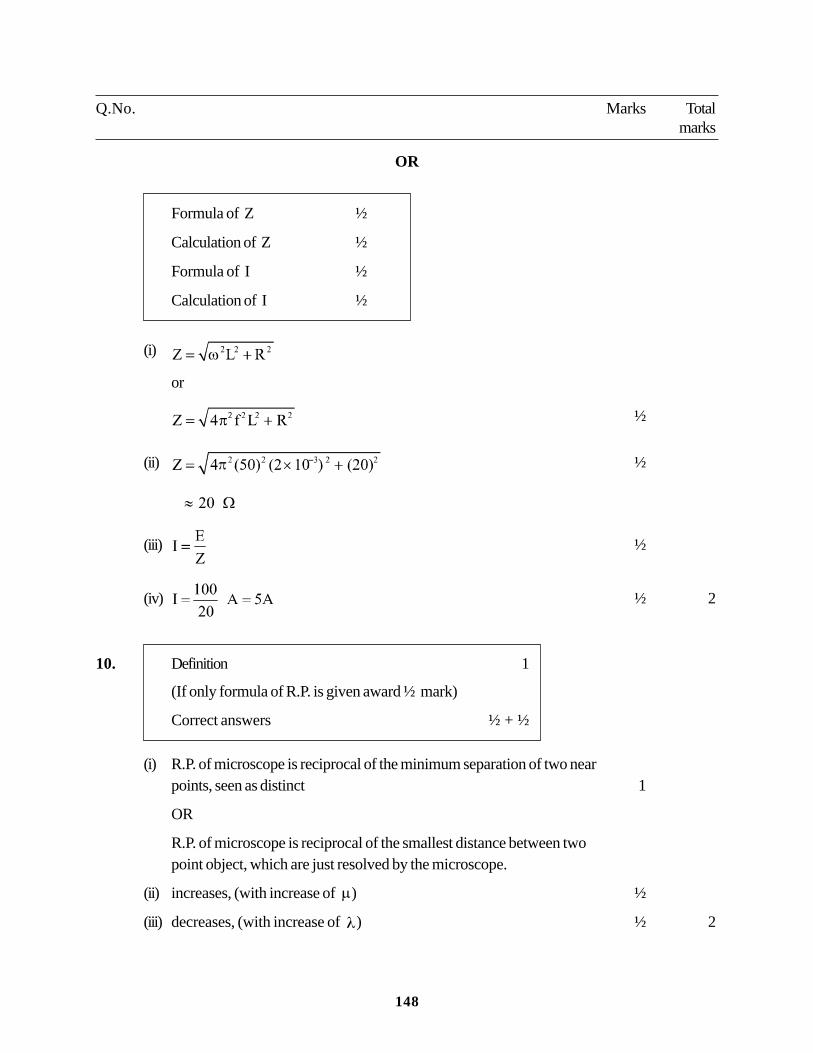
148
OR
Formula of Z ½
Calculation of Z ½
Formula of I ½
Calculation of I ½
(i)
or
½
(ii) ½
(iii) ½
(iv) ½ 2
10. Definition 1
(If only formula of R.P. is given award ½ mark)
Correct answers ½ + ½
(i) R.P. of microscope is reciprocal of the minimum separation of two nearpoints, seen as distinct 1
OR
R.P. of microscope is reciprocal of the smallest distance between twopoint object, which are just resolved by the microscope.
(ii) increases, (with increase of ) ½
(iii) decreases, (with increase of ) ½ 2
Q.No. Marks Totalmarks
149
11. Graph 1
Correct answers ½ + ½
(i) Graph :
1
(ii) for r > r0 Attraction ½
(iii) for r < r0
Repulsion ½ 2
12. Correct Answer 1
Graph 1
(If X and Y are correctly identified but the identification of biasing is incorrector not given at all, award ½
mark only.)
(X p-Type)(Y n-Type) 1
(i) Reverse biased
(ii) Graph :
1 2
Q.No. Marks Totalmarks
150
13. Statement 1
Diagram ½
Derivation 1½
Statement :
Net electric flux through to a closed surface is equal to times the totalnet charge enclosed within the surface. 1
(If the student just writes , award 1/2 mark only)
(ii) Diagram:-
½
(iii) Derivation:-
½
Also, (where is charge per unit length)
OR ½
OR ½ 3
Q.No. Marks Totalmarks
151
14. Principle and Explanation 1½
Expression forField ½Potential Difference ½Capacitance ½
Principle:
(i) When an uncharged, grounded conducting plate is placed near a chargedconducting plate a charge, of the opposite sign, gets induced on thesecond plate. 1½
(ii) This reduces the potential of first plate, without any change in the chargepresent in it.
(iii) This increases the capacitance.
½
½
½ 3
15. 2 Reasons for fault ½ + ½Causes and reason for more deflection at B ½ + ½Causes and reason for less deflection at ‘B’ ½ + ½
Possible Faults
(a) The negative terminal of is connected to point X. ½
(b) ½
(i) If galvanometer shows more defection at B
Cause : Negative terminal of is connected to X ½
Reason : Potential difference across wire and the cell send current throughthe galvanometer in the same sense and the galvanometer deflection increaseswith an increase in the length of the wire. ½(iii) If galvanometer shows less deflection at B
Cause : ½
Reason : Potential difference across the potentiometer wire opposes andcurrent in galvanometer decreases with an increase in the length of the wire. ½ 3
Q.No. Marks Totalmarks
152
OR
Circuit with current distribution 1
Writing two correct loop equation ½ + ½
Result 1
1
Loop Equations( Loop ABDA) – I
1R
1 – IgRg + (I – I
1)R
3=0 ½
(Loop BCDB) – ( I1 – Ig ) R
2 + (I – I
1 + Ig ) R
4 + Ig Rg =0 ½
(or any equivalent equations)
Derivation of Resultas Ig=0, I
1R
1= (I –I
1) R
3
I1 R
2= (I – I
1) R
4
1 3
16. Seebeck Effect 1
Graph 1
Explanation ½+½
When two dissimilar metals are joined together to form two junctions, and these
are kept at different temperatures, a net emf develops in the system. 1
Graph :
1
Q.No. Marks Totalmarks
153
Neutral temperature unaffected ½
Temperature of inversiondecreases ½ 3
17. Correct Identification of each radiation ½ + ½ + ½
One more application of each (other than given one) ½+ ½ + ½
(i) Radiation: Infrared ½Application: night vision/ Thermal Sensor/ Green house effect/
relieve in muscular pain/ in remote control devices ½
(ii) Radiation: U.V radiation ½Application: food preservation/ water purification/ forensic
science/ sterilization of surgical instruments ½
(iii) Radiation: X-rays ½Application: Medical diagonosis/ detection of mechanical fault/
radio therapy detectors/ study of crystal structure ½ 3
18. Formula ½ + ½ +½(for f, v, I each)
Substitution and correct result ½ + ½ +½
½
OR
f = 25 cm ½
½
½
OR
½
½ 3
Q.No. Marks Totalmarks
154
19. Schematic diagram 1 ½
Explanation 1 ½
1½
key points for brief explanation:
(a) accelerated electrons are scattered by Nicol crystal and collected bycollector which is connected to the galvanometer.
(b) Strong peak of intensity(current) appeared for accelerating potential of54 V, at a scattering angle of 50o.
(c) Wavelength value, obtained by diffraction measurement of electrons, is inexcellent agreement with the de- Broglie wavelength of electrons
accelerated through a potential difference of 54V. 1½ 3
20. Graph 1
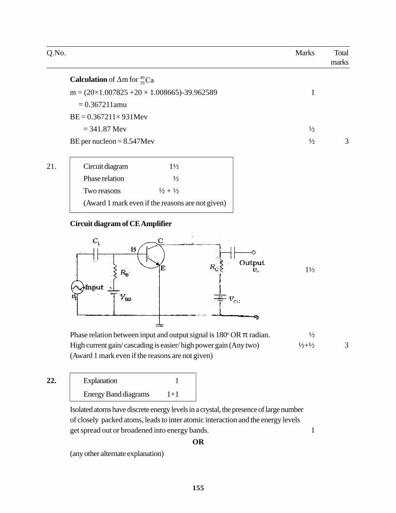
Calculation of m 1
Calculation of BE ½
BE per nucleon ½
Graph :
1
Q.No. Marks Totalmarks
155
Calculation of m for
m = (20×1.007825 +20 × 1.008665)-39.962589 1
= 0.367211amu
BE = 0.367211× 931Mev
= 341.87 Mev ½
BE per nucleon = 8.547Mev ½ 3
21. Circuit diagram 1½
Phase relation ½
Two reasons ½ + ½
(Award 1 mark even if the reasons are not given)
Circuit diagram of CE Amplifier
1½
Phase relation between input and output signal is 180o OR π radian. ½High current gain/ cascading is easier/ high power gain (Any two) ½+½ 3(Award 1 mark even if the reasons are not given)
22. Explanation 1
Energy Band diagrams 1+1
Isolated atoms have discrete energy levels in a crystal, the presence of large numberof closely packed atoms, leads to inter atomic interaction and the energy levelsget spread out or broadened into energy bands. 1
OR
(any other alternate explanation)
Q.No. Marks Totalmarks
156
1
1 3
23. Definition 1Explaining the need of modulation 1Diagram for PAM and PDM ½ + ½
A Process by which some characteristic of the transmitted carrier wave isvaried in accordance with the information message signal 1 (i) To design antenna of practicable size.(ii) to avoid intermixing of different signals(iii) to increase power radiation by antenna(iv) to increase the operating range. (Any one) 1
LASER = Light Amplification by Stimulated Emission of Radiation 1
Reasons:(1) Highly energetic
(2) Monochromatic
(3) Coherent
(4) Highly directional
(5) Size compatible with that of optical fiber
(6) Emitted light can be modulated by small variations in the informationsignal voltage
(7) Thermal stability
(Any Four) ½×4 = 2 3
25. Diagram 1
Principle 1
Construction 1
Derivation 1½
Interpretation ½
Principle:A beam of charged particles describes a circular path when subjected to a uniformmagnetic field directed perpendicular to their plane of motion. The beam can beaccelerated time and again by a high frequency electric field of correctly adjustedfrequency applied between two dees. 1
Q.No. Marks Totalmarks
158
Construction :Consists of two semi circular disc like metal containers D
1 and D
2 connected to
high frequency alternating voltage 1A magnetic field is applied perpendicular to the plane of the dees.Derivation
1½
Interpretation :Frequency does not depend on the speed of the charged particle ½ 5(Any other correct alternate method)
OR
Distinguishing for each property 1+1+ ½One example for each type ½ + ½ + ½Diagrams ½ + ½(Even if coercivity is not mentioned award ½ mark)
Dia Para Ferro
(i) Susceptibility Very small and Small and negative High and Positive 1negative
(ii) Permeability Less than one Greater than onevery large 1compared to one ½
(iii) Coercivity — — Exists
Example one each Bi,Cu,Pb,Si,N,Al, Na, Ca, O, Fe, Ni, Co and ½+½½H
Definition :Inductive reactance is a measure of the opposition offered by the given inductorto the flow of any alternating current. 1
Graph :
1
Derivation :
½
½
½
or 1
Current lags behind the volage by a phase angle of . ½ 5
½
½ 5
Indu
ctiv
e re
acta
nce
Frequency
160
OR
Definition 1Graph 1Derivation & Conclusions 2½+½
Definition :Capacitive reactance is measure of the opposition offered by a capacitor tothe flow of an alternating current through it. 1
Graph :
1
Derivation :
½
½
put . Also ½
1
I leads E in phase by π/2 ½ 5
27. Condition 1Diagram 1Explanation 2Sketch of the pattern 1
Condition :Size of the obstacle /aperture should be comparable with the wave length of theincident light. 1
Diagram :
1
Frequency
Cap
aciti
vere
act
an
ce
161
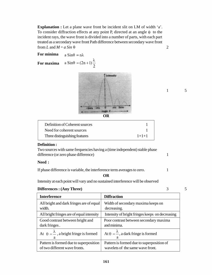
Explanation : Let a plane wave front be incident slit on LM of width ‘a’.To consider diffraction effects at any point P, directed at an angle to theincident rays, the wave front is divided into a number of parts, with each parttreated as a secondary wave front Path difference between secondary wave frontfrom L and M = a Sin 2
For minima
For maxima
1 5
OR
Definition of Coherent sources 1Need for coherent sources 1Three distinguishing features 1+1+1
Definition :Two sources with same frequencies having a (time independent) stable phasedifference (or zero phase difference) 1
Need :
If phase difference is variable, the interference term averages to zero. 1OR
Intensity at each point will vary and no sustained interference will be observed
Differences : (Any Three) 3 5
Interference Diffraction
All bright and dark fringes are of equal Width of secondary maxima keeps onwidth. decreasing.
All bright fringes are of equal intensity Intensity of bright fringes keeps on decreasing
Good contrast between bright and Poor contrast between secondary maximadark fringes . and minima.
At , a bright fringe is formed At , a dark fringe is formed
Pattern is formed due to superposition Pattern is formed due to superposition ofof two different wave fronts. wavelets of the same wave front.