Chapter 3 Classical and Quantum Circuit Theory A noisy electrical network can be represented by a noise-free network with external noise generators. The magnitude of the external noise generator is expressed either by an equiv- alent noise resistance or an equivalent noise temperature. When a network is dominated by the granular property of changed carriers, the noise generator is more conveniently described by a shot noise suppression factor. If such a network has four terminals or two (input and output) ports, the noise figure is often used as a figure of merit expressing the inherent noisiness of the circuit. The technique is particularly useful to analyze a cascaded amplifier system. The linear or linearized network technique is also useful to express the quantum noise properties of complicated quantum systems. Most of the arguments in this chapter follow the excellent text on the circuit model of noise by H.A. Haus [1]. 3.1 Two-Terminal Networks –Thevenin Equivalent Circuit– A noisy two-terminal network with impedance Z (ω)= R(ω)+ iX (ω) generates the open circuit voltage fluctuation v(t) as shown in Fig. 3.2 (a). The two equivalent circuits based on Thevenin’s theorem[2] are shown in Fig. 3.2 (b) and (c). One is the noise-free network with impedance Z (ω) in series with a voltage generator v(t). The other is the noise-free network with admittance Y (ω)= G(ω)+ iB(ω) in parallel with a current generator i(t). Consider the parallel RC circuit shown in Fig. 3.1 (a) as an example of such a two terminal network. The noise of the register is represented by the parallel current source i(t) with the spectral density of S i (ω). The series voltage source v(t) in the Thevenin equivalent circuit shown in Fig. 3.1 (b) has then the spectral density of S v (ω)= R 2 1+ ω 2 (CR) 2 S i (ω) . (3.1) The frequency dependent (Lorentzian) power spectral density Eq. (3.1) is due to the impedance of the capacitor. We assume the spectrum S i (ω) is constant and flat in a frequency range of interest. Using the Wiener-Khintchine theorem, or more specifically Parseval theorem of Chapter 1, we obtain the mean-square value of the voltage noise hv 2 i = 1 2π Z ∞ 0 S v (ω)dω = R 4C S i (ω) . (3.2) 1
Transcript
Chapter 3
Classical and Quantum CircuitTheory
A noisy electrical network can be represented by a noise-free network with external noisegenerators. The magnitude of the external noise generator is expressed either by an equiv-alent noise resistance or an equivalent noise temperature. When a network is dominatedby the granular property of changed carriers, the noise generator is more convenientlydescribed by a shot noise suppression factor. If such a network has four terminals or two(input and output) ports, the noise figure is often used as a figure of merit expressing theinherent noisiness of the circuit. The technique is particularly useful to analyze a cascadedamplifier system. The linear or linearized network technique is also useful to express thequantum noise properties of complicated quantum systems. Most of the arguments in thischapter follow the excellent text on the circuit model of noise by H.A. Haus [1].
A noisy two-terminal network with impedance Z(ω) = R(ω) + iX(ω) generates the opencircuit voltage fluctuation v(t) as shown in Fig. 3.2 (a). The two equivalent circuits basedon Thevenin’s theorem[2] are shown in Fig. 3.2 (b) and (c). One is the noise-free networkwith impedance Z(ω) in series with a voltage generator v(t). The other is the noise-freenetwork with admittance Y (ω) = G(ω) + i B(ω) in parallel with a current generator i(t).
Consider the parallel RC circuit shown in Fig. 3.1 (a) as an example of such a twoterminal network. The noise of the register is represented by the parallel current sourcei(t) with the spectral density of Si(ω). The series voltage source v(t) in the Theveninequivalent circuit shown in Fig. 3.1 (b) has then the spectral density of
Sv(ω) =R2
1 + ω2(CR)2Si(ω) . (3.1)
The frequency dependent (Lorentzian) power spectral density Eq. (3.1) is due to theimpedance of the capacitor. We assume the spectrum Si(ω) is constant and flat in afrequency range of interest. Using the Wiener-Khintchine theorem, or more specificallyParseval theorem of Chapter 1, we obtain the mean-square value of the voltage noise
〈v2〉 =12π
∫ ∞
0Sv(ω)dω =
R
4CSi(ω) . (3.2)
1
Figure 3.1: (a) A parallel RC circuit with thermal noise current source. (b)The Thevenin equivalent circuit with thermal noise voltage source.
The energy stored in the capacitor is thus equal to
12C〈v2〉 =
18RSi(ω) . (3.3)
According to the equipartition theorem[3], if the system energy is of the form of quadraticdependence on generalized coordinate (the voltage in this case), the average energy of thesystem under thermal equilibrium condition is equal to 1
2kBθ per degree of freedom. Thismeans current spectral density must be given by
Si(ω) =4kBθ
R. (3.4)
This is Johnson-Nyguist thermal noise of a simple register which we will discuss in thenext section. Notice that the noise energy 1
2kBθ is independent of the resistance R whilethe magnitude and the bandwidth of the noise spectrum are dependent on R.
In a more general content, the single-sided power spectral density of v(t) in Fig. 3.2(b)is often expressed by
Sv(ω) = 4kbθRn , (3.5)
where θ is the absolute temperature and Rn is the equivalent noise resistance.The spectral density of i(t) is in Fig. 3.2(c) expressed by
Si(ω) = 4kbθGn , (3.6)
where Gn is the equivalent noise conductance.If the network is linear and passive, and there is no net energy flow, i.e. the circuit is at
thermal equilibrium condition, then Rn = R(ω) and Gn = G(ω) = R(ω)/[R(ω)2 +X(ω)2].The noise in this case is reduced to Johnson-Nyquist thermal noise, as mentioned above.However, in nonlinear active circuits, or in non-equilibrium condition with a net energyflow, these equalities generally do not hold. This is due to the fact that equipartitiontheorem of statistical mechanics, on which Johnson-Nyquist thermal noise is based, doesnot hold for a non-equilibrium system.
2
Figure 3.2: (a) A noisy two-terminal network. (b) Thevenin equivalent cir-cuit with an external voltage source. (c) Thevenin equivalent circuit with anexternal current source.
When the electron temperature is different from the lattice temperature, which isthe case for hot electron devices, it is convenient to express Eqs. (3.5) and (3.6) in thealternative forms:
Sv(ω) = 4kBθnR , (3.7)
Si(ω) = 4kBθnG , (3.8)
where θn is the equivalent noise temperature. In circuits containing shot noise sources asprimary noise sources, it is convenient to use the expression
Si(ω) = 2qξI , (3.9)
where I is the terminal current and ξ is the shot noise suppression factor. If some smooth-ing mechanisms are dominant, for instance due to space charge effect, ξ becomes smallerthan unity. If there is no smoothing mechanism in the system, the power spectral densityis full-shot noise (ξ = 1).
Next let us consider a parallel LCR circuit shown in Fig. 3.3. The open circuit voltageυ(t) has the spectral density of
Sυ(ω) =[
1R2
+(ωC − 1
ωL
)2]−1
Si(ω) . (3.10)
Sυ(ω) now concentrates on the resonant frequency ω0 = 1√LC
of a LC circuit and decaystoward ω = 0 and ω = ∞. Using the Parseval theorem, we obtain the mean-square valueof the voltage generator
〈v2〉 =12π
∫ ∞
0Sυ(ω)dω =
kBθ
C, (3.11)
3
which is identical to Eq. (3.2), even though the spectral shape Eq. (3.10) is very differentfrom Eq. (3.1). The energy stored in the system is now given by
12C〈υ(t)2〉+
12L〈i(t)2〉 =
12kBθ +
12L
[〈υ(t)2〉ω2
0L2
]
= kBθ . (3.12)
We have two degrees of freedom in this system (the voltage across the capacitor and thecurrent through the inductor), so the average thermal energy is doubled.
Figure 3.3: A parallel LCR circuit with thermal noise current source.
3.2 Four-Terminal Networks (Two Ports)
A network with two pairs of terminals, input and output ports, is known as a four-terminalor two-port network. For a noiseless four-terminal network, the currents and voltages at theterminals are related to each other in terms of the impedance matrix Z or the admittancematrix Y as follows: (
V1
V2
)=
(Z11 Z12
Z21 Z22
) (I1
I2
), (3.13)
(I1
I2
)=
(Y11 Y12
Y21 Y22
) (V1
V2
). (3.14)
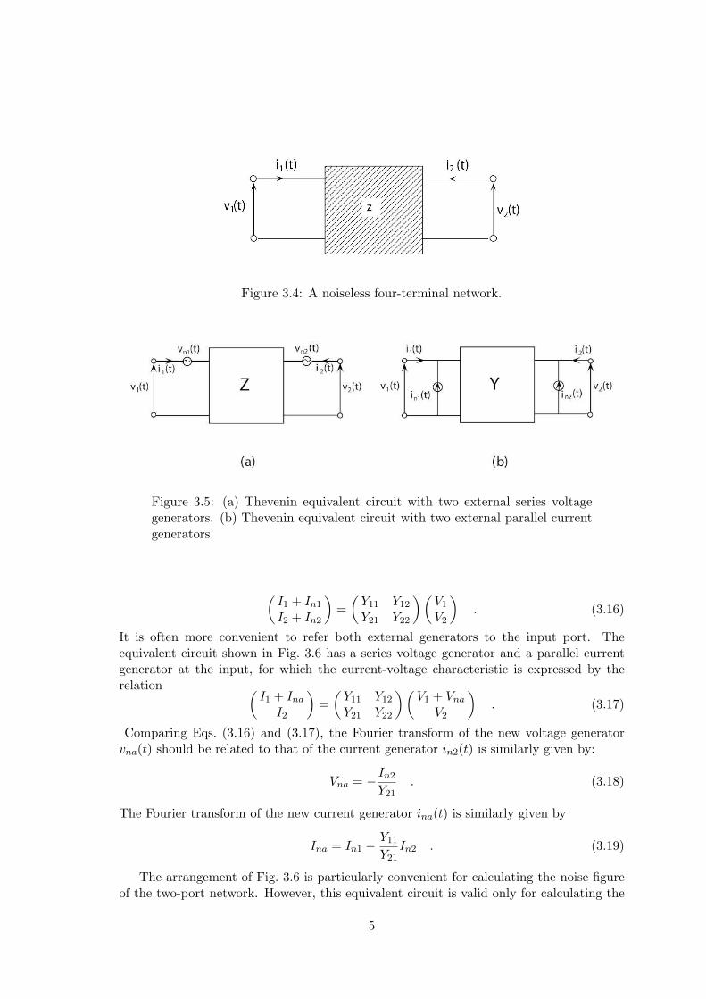
The subscripts 1 and 2 refer to the input and output ports, respectively, and the signconvention is that currents flowing into the network are positive, as shown in Fig. 3.4.The upper case letters I and V indicate the Fourier transforms of the time dependentcurrent and voltage, which are in general dependent on frequency.
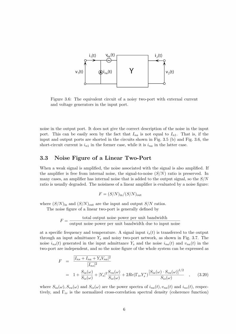
A noisy four-terminal network is represented by an extension of Thevenin’s theorem[2].In Fig. 3.5 (a), a series noise voltage generator appears at each port. Some degree of cor-relation may exist between these two generators since the same internal noise mechanismmay be responsible, at least in part, for the open circuit voltage fluctuations at the twoterminals. The dual of Fig. 3.5 (a) is shown in Fig. 3.5 (b), in which the internal noise isrepresented by external parallel current generators.
The current-voltage relation of a noisy four-terminal network becomes(
V1 + Vn1
V2 + Vn2
)=
(Z11 Z12
Z21 Z22
) (I1
I2
), (3.15)
4
Figure 3.4: A noiseless four-terminal network.
Figure 3.5: (a) Thevenin equivalent circuit with two external series voltagegenerators. (b) Thevenin equivalent circuit with two external parallel currentgenerators.
(I1 + In1
I2 + In2
)=
(Y11 Y12
Y21 Y22
) (V1
V2
). (3.16)
It is often more convenient to refer both external generators to the input port. Theequivalent circuit shown in Fig. 3.6 has a series voltage generator and a parallel currentgenerator at the input, for which the current-voltage characteristic is expressed by therelation (
I1 + Ina
I2
)=
(Y11 Y12
Y21 Y22
) (V1 + Vna
V2
). (3.17)
Comparing Eqs. (3.16) and (3.17), the Fourier transform of the new voltage generatorvna(t) should be related to that of the current generator in2(t) is similarly given by:
Vna = − In2
Y21. (3.18)
The Fourier transform of the new current generator ina(t) is similarly given by
Ina = In1 − Y11
Y21In2 . (3.19)
The arrangement of Fig. 3.6 is particularly convenient for calculating the noise figureof the two-port network. However, this equivalent circuit is valid only for calculating the
5
Figure 3.6: The equivalent circuit of a noisy two-port with external currentand voltage generators in the input port.
noise in the output port. It does not give the correct description of the noise in the inputport. This can be easily seen by the fact that Ina is not equal to In1. That is, if theinput and output ports are shorted in the circuits shown in Fig. 3.5 (b) and Fig. 3.6, theshort-circuit current is in1 in the former case, while it is ina in the latter case.
3.3 Noise Figure of a Linear Two-Port
When a weak signal is amplified, the noise associated with the signal is also amplified. Ifthe amplifier is free from internal noise, the signal-to-noise (S/N) ratio is preserved. Inmany cases, an amplifier has internal noise that is added to the output signal, so the S/Nratio is usually degraded. The noisiness of a linear amplifier is evaluated by a noise figure:
F = (S/N)in/(S/N)out
where (S/N)in and (S/N)out are the input and output S/N ratios.The noise figure of a linear two-port is generally defined by
F =total output noise power per unit bandwidth
output noise power per unit bandwidth due to input noise
at a specific frequency and temperature. A signal input is(t) is transferred to the outputthrough an input admittance Ys and noisy two-port network, as shown in Fig. 3.7. Thenoise ins(t) generated in the input admittance Ys and the noise ina(t) and vna(t) in thetwo-port are independent, and so the noise figure of the whole system can be expressed as
F =|Ins + Ina + YsVna|2
|Ins|2
= 1 +Sia(ω)Sis(ω)
+ |Ys|2 Sva(ω)Sis(ω)
+ 2Re(ΓivY∗s )
[Sia(ω) · Sva(ω)]1/2
Sis(ω), (3.20)
where Sia(ω), Sva(ω) and Sis(ω) are the power spectra of ina(t), vna(t) and ins(t), respec-tively, and Γiv is the normalized cross-correlation spectral density (coherence function)
6
Figure 3.7: A circuit for calculating the noise figure of a two-port network.
between ina(t) and vna(t),
Γ∗iv(ω) =I∗naVna
[|Ina|2 · |Vna|2
] 12
=Siva(ω)
[Sia(ω)Sva(ω)]12
. (3.21)
The power spectral densities can be expressed as
Sia(ω) = 4kBθGni , (3.22)
Sva(ω) = 4kBθ/Gnv , (3.23)
Sis(ω) = 4kBθGs . (3.24)
Here Gni and Gnv are the equivalent noise conductances, which are not necessarily actualconductances of the two-port network. On the other hand, Gs = Re(Ys) is the actualsource conductance. In the spirit of Eqs. (3.18) and (3.19), the current generator ina(t)is split into two parts, one part of which is uncorrelated with vna(t) and the other part isfully correlated with vna(t). Therefore we obtain
Ina = Inb + YcVna , (3.25)
where Yc is called the correlation admittance of ina(t) and vna(t). Since InbV ∗na = 0, we
have
Γiv ≡ InaV ∗na[
|Ina|2 |Vna|2]1/2
= Yc
[|Vna|2|Ina|2
]1/2
=Yc√
GniGnv. (3.26)
The noise figure of Eq. (3.20) is now rewritten as
F = 1 +Gni
Gs+
(Gs + Gc)2 + (Bs + Bc)2 − (G2c + B2
c )GnvGs
, (3.27)
where Gc and Bc are the real and imaginary parts of the correlation admittance Yc. Theoptimum source admittance to minimize the noise figure and the minimum noise figureare obtained by the conditions:
∂F
∂Bs= 0 and
∂F
∂Gs= 0 .
7
Using this technique, Eq. (3.27) is easily transformed into the form
F = F0 +(Gs −Gso)2 + (Bs −Bso)2
GnvGs. (3.28)
Here, F0 = 1 + 2Gnv
(Gso + Gc) is the minimum noise figure achieved when the sourceadmittance satisfies the following matching condition:
Gs = Gso = (GnvGni −B2c )1/2 , (3.29)
Bs = Bso = −Bc . (3.30)
The conditions Eqs. (3.29) and (3.30) for the source conductance and susceptance arereferred to as noise tuning or noise matching. The noise figure increases quadraticallywhen Gs and Bs are deviated from the optimum values. The four parameters Fo, Gso,Bso and Gnv completely characterize the noise of the two-port network.
The measurement of these four parameters and full characterization for a given lineartwo-port runs as follows:
1. Adjust the source conductance Gs and susceptance Bs to achieve the minimum noisefigure F0. The three parameters F0, Gs0 and Bs0 can be directly obtained in thisnoise matching process.
2. Make a measurement of the noise figure at some non-optimum source admittance(Gs 6= Gs0 and/or Bs 6= Bs0). The remaining parameter Gnυ can be obtained fromF − F0.
3. Three other parameters Bc, Gni and Gc to fully characterize Eq. (3.27) are obtainedfrom Eqs. (3.29), (3.30) and Gc = Gnυ
2 (F0 − 1)−Gs0 .
4. Calculate the power spectral densities Sia(ω) and Sυa(ω) from Eqs. (3.22) and (3.23)and Γiυ from Eq. (3.26).
If an amplifier is noise-free, the noise figure takes a lower bound, F0 = 1.
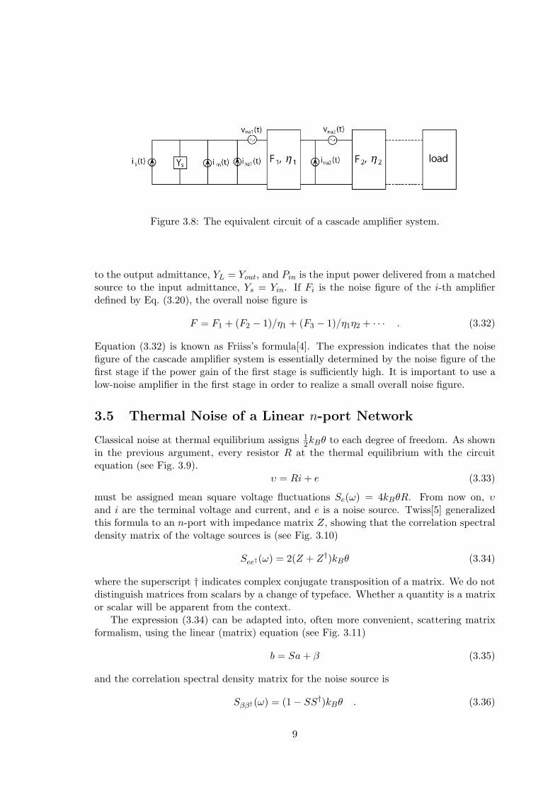
3.4 Noise Figure of Amplifiers in Cascade
One of the important applications of the equivalent circuit discussed in the previous sectionis the overall noise figure of the system when several amplifiers are connected in cascade asshown in Fig. 3.8. Suppose each amplifier in the cascade is connected to a matched load,i.e. the output and input admittances of adjoining amplifiers are equal: Y1,out = Y2,in =Y1 , Y2,out = Y3,in = Y2, and so on. The noise figure of the whole system in such a casecan be written as
F =|Isn + Ina1 + YsVna1|2
|Ins|2+|Ina2 + Y1Vna2|2
η1|Ins|2+|Ina3 + Y2Vna3|2
η1η2|Ins|2+ · · · . (3.31)
Here Yi and ηi are the output admittance and power gain of the i-th amplifier. The powergain η is defined by Pout/Pin, where Pout is the output power delivered to a matched load
8
Figure 3.8: The equivalent circuit of a cascade amplifier system.
to the output admittance, YL = Yout, and Pin is the input power delivered from a matchedsource to the input admittance, Ys = Yin. If Fi is the noise figure of the i-th amplifierdefined by Eq. (3.20), the overall noise figure is
F = F1 + (F2 − 1)/η1 + (F3 − 1)/η1η2 + · · · . (3.32)
Equation (3.32) is known as Friiss’s formula[4]. The expression indicates that the noisefigure of the cascade amplifier system is essentially determined by the noise figure of thefirst stage if the power gain of the first stage is sufficiently high. It is important to use alow-noise amplifier in the first stage in order to realize a small overall noise figure.
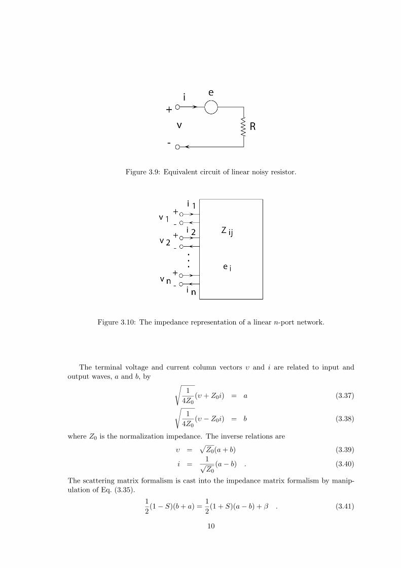
3.5 Thermal Noise of a Linear n-port Network
Classical noise at thermal equilibrium assigns 12kBθ to each degree of freedom. As shown
in the previous argument, every resistor R at the thermal equilibrium with the circuitequation (see Fig. 3.9).
υ = Ri + e (3.33)
must be assigned mean square voltage fluctuations Se(ω) = 4kBθR. From now on, υand i are the terminal voltage and current, and e is a noise source. Twiss[5] generalizedthis formula to an n-port with impedance matrix Z, showing that the correlation spectraldensity matrix of the voltage sources is (see Fig. 3.10)
See†(ω) = 2(Z + Z†)kBθ (3.34)
where the superscript † indicates complex conjugate transposition of a matrix. We do notdistinguish matrices from scalars by a change of typeface. Whether a quantity is a matrixor scalar will be apparent from the context.
The expression (3.34) can be adapted into, often more convenient, scattering matrixformalism, using the linear (matrix) equation (see Fig. 3.11)
b = Sa + β (3.35)
and the correlation spectral density matrix for the noise source is
Sββ†(ω) = (1− SS†)kBθ . (3.36)
9
Figure 3.9: Equivalent circuit of linear noisy resistor.
Figure 3.10: The impedance representation of a linear n-port network.
The terminal voltage and current column vectors υ and i are related to input andoutput waves, a and b, by
√1
4Z0(υ + Z0i) = a (3.37)
√1
4Z0(υ − Z0i) = b (3.38)
where Z0 is the normalization impedance. The inverse relations are
υ =√
Z0(a + b) (3.39)
i =1√Z0
(a− b) . (3.40)
The scattering matrix formalism is cast into the impedance matrix formalism by manip-ulation of Eq. (3.35).
12(1− S)(b + a) =
12(1 + S)(a− b) + β . (3.41)
10
Figure 3.11: Scattering matrix representation of a n-port network.
Comparison of Eq. (3.41) with the impedance formulation
υ = Zi + e (3.42)
gives
Z = (1− S)−1(1 + S)Z0 (3.43)e = 2
√Z0(1− S)−1β . (3.44)
The correlation spectral density matrix of e is
See†(ω) = 4Z0(1− S)−1Sββ†(ω)(1− S†)−1
= 4Z0(1− S)−1(1− SS†)(1− S†)−1kBθ . (3.45)
Let us check the expression for
Z + Z† = Z0
[(1− S)−1(1− S) + (1 + S†)(1− S†)−1
]. (3.46)
Multiplying by (1− S) from the left and by (1− S†) from the right we obtain
(1− S)(Z + Z†)(1− S†) = Z0
[(1 + S)(1− S†) + (1− S)(1 + S†)
]
= 2Z0[1− SS†] . (3.47)
Thus, we have proven that
2Z0(1− S)−1(1− SS†)(1− S†)−1 = Z + Z† . (3.48)
Using this fact, we have for Eq. (3.45)
See†(ω) = 2(Z + Z†)kBθ . (3.49)
11
3.6 Quantum Circuit Theory
If an optical wave propagates in a complicated noisy system, a noise equivalent circuitmodel introduced in sec.(3.5) also provides a convenient tool. However, since h̄ω À kBθat optical frequencies, quantum mechanical zero-point fluctuation dominates over thermalnoise. We need to establish a new rule to handle such a quantum system.
Linear quantum systems with loss must contain noise sources in order to provide forconservation of commutator brackets, which would decay to zero in the absence of suchsources[6]. This property is analogous to that of lossy systems at thermal equilibriumwhich would lose their thermal excitation were it not for the thermal noise sources inthe lossy element, which was first introduced by Langevin[7]. The noise sources associ-ated with loss are simply a manifestation of the fluctuation-dissipation theorem[8]. Linearphase-insensitive systems with gain contain noise sources as well[1] because, if noise werenot present, classical measurements could be performed on the amplified output, per-forming simultaneous measurements on two noncommuting observables (say in-phase andquadrature field components) with no increase in uncertainty, in violation of the dou-bling of uncertainty associated with a simultaneous measurement of two noncommutingobservables[9]. Phase-sensitive systems with gain do not necessarily permit a simultaneousmeasurement, and thus do not necessarily contain noise sources[10].
The Langevin noise sources are particularly well adapted to a circuit theoretical treat-ment of linear systems. Much work has been done in classical systems, such as oscillatorsand amplifiers, using the terminology of electrical circuit theory[11]. Therefore, it is ad-vantageous to express the terminology of quantum electrodynamics in circuit “language.”
3.6.1 Analogy of Thermal Noise with Commutator Bracket Conserva-tion
A quantum-mechanical linear circuit has to obey commutator bracket conservation. Theinput and output wave amplitudes, a and b in Fig. 3.11 are now considered as the photonannihilation operators. The standard commutator of a single-mode field operator a is
[a, a+] = 1 (3.50)
where the normalization is such that < a+a > gives the expectation of photon number.We can renormalize the photon annihilation and creation operators in such a way,
[a, a+] = h̄ω (3.51)
is satisfied, where the normalization of < a+a > is to energy. Here, the superscript +indicates the Hermitian adjoint of the operator. If a quantum system is characterized bythe scattering coefficient Γ for a single (scalar) incident wave a and reflected wave b, anoise source β has to be assigned to conserve commutators:
b = Γa + β . (3.52)
because the output wave must satisfy the same commutator bracket as (3.51):
[b, b+] = |Γ|2[a, a+] + [β, β+] = h̄ω . (3.53)
12
One then finds for the commutator of the noise source
[β, β+] = (1− |Γ|2)h̄ω . (3.54)
Note that [β, β+] is negative, when the system has gain (|Γ|2 > 1). In this case βmust be interpreted as a creation operator, β+ as an annihilation operator. The noisecomponents can be separated into in-phase and quadrature components
β1 =12(β + β+) and β2 =
i
2(β+ − β) . (3.55)
The mean square fluctuations of β1 are
〈∆β21〉 =
14〈(β + β+)2〉 − 1
4〈(β + β+)〉2
=14〈(β + β+)2〉 (3.56)
because the expectation value of the noise β + β+ is zero. Thus
〈∆β21〉 =
14〈β+β+ + ββ + ββ+ + β+β〉
=14〈β+β+ + ββ + 2ββ+〉 − 1
4[β, β+]
=14〈β+β+ + ββ + 2β+β〉+
14[β, β+] . (3.57)
Suppose that the reservoir responsible for the noise source is in the ground state. Thisassumption corresponds to an ideal attenuator and amplifier which impose a minimumallowable noise on the signal. The expectation values of β+β+ and ββ are then zero.Further, 〈β+β〉 is zero when β is an annihilation operator (|Γ|2 < 1). Then
〈∆β21〉 = (1− |Γ|2)1
4h̄ω . (3.58)
When |Γ|2 > 1 and β is interpreted as a creation operator, then 〈ββ+〉 is zero, and
〈∆β21〉 = (|Γ|2 − 1)
14h̄ω . (3.59)
An analogous derivation for 〈∆β22〉 shows that
〈∆β22〉 = 〈∆β2
1〉 (3.60)
for the present case of phase-insensitive quantum systems.The generalization of the scattering relation (3.54) to passive n-ports is easy. Classi-
cally, Eq. (3.36) expresses the self- and cross-correlation spectra by the formula
Sβiβ∗j (ω) = (1− SS†)ijkBθ (3.61)
Quantum mechanically we ask for the commutator
[βi , β+j ] = βiβ
+j − β+
j βi (3.62)
13
which has no classical analog, because classically the expression is zero. From Eq. (3.35),one has
bib+j = Sikaka
+l S∗jl + βiβ
+i . (3.63)
Similarly,b+j bi = Sika
+l akS
∗jl + β+
i βi . (3.64)
Note that only the operators have been reversed in order, not the matrix multipliers.Therefore,
[bi , b+j ] = h̄ωSikS
∗jk + [βi , β+
j ] = h̄ω . (3.65)
We denote by the dagger the Hermitian adjoint of an operator as well as the conjugatetranspose of the matrix, whose elements are the operators. Then, one may write Eq. (3.65)in matrix form
[β , β+] = [1− SS†]h̄ω . (3.66)
This is the generalization of (3.54) for a single port circuit.
3.6.2 The Characteristic Noise Matrix
To see more clearly what is involved in the transition from a system with loss to a systemwith gain, consider the case of uncoupled resistors, or reflectors. Then (1−SS†) is diagonaland Sββ†(ω) is also diagonal. The characteristic noise matrix[12] defined by
N ≡ Sββ†(ω)(SS† − 1)−1 (3.67)
is diagonal and has all diagonal elements (eigenvalues) equal to −kBθ for a classical case.If one or more reflections have gain, an equivalent noise temperature can be assigned tothe noise source associated with each of the reflections. The noise temperature should beconsidered negative[13]. Then,
Sβi(ω) ≡ (1− |Sii|2)kBθi (3.68)
is a positive quantity, as it must be. Negative temperatures have been assigned to invertedmedia[14].
A lossless (noise-free) imbedding of the network (Fig. 3.12) is represented by a unitarytransformation and therefore, leaves the eigenvalues of the characteristic noise matrixinvariant.
In the quantum-mechanical case one may define two different characteristic “noisematrices.” One is more properly called characteristic commutator matrix NC and can bedefined by
NC ≡ [β , β†](SS† − 1)−1 = −Ih̄ω . (3.69)
Here I is an identity matrix. This matrix has all identical eigenvalues of −h̄ω and thusis proportional to the identity matrix. The transformation of NC by a lossless imbed-ding network follows the same laws as those of N , and thus is unitary. Therefore thecommutator matrix remains diagonal after such an imbedding.
In analogy with Eq. (3.67) one may define a characteristic noise matrix for the quantum-mechanical system. The commutators fix the minimum amount of noise that must be as-sociated with a particular reflection, or resistor. Indeed, since for the uncoupled network
[βi , β†i ] = [1− |Sii|2]h̄ω (3.70)
14
Figure 3.12: A lossless “imbedding.”
then, with the states of the operators βi’s in the ground states, one finds
〈β2i 〉 ≡ 1
2〈βiβ
+i + β+
i βi〉
= (1− |Sii|2)12 h̄ω (3.71)
when |Sii| < 1 and
〈β2i 〉 =
12〈βiβ
+i + β+
i βi〉
= (|Sii|2 − 1)12h̄ω (3.72)
for |Sii| > 1. The characteristic noise matrix of the uncoupled network is diagonal andhas eigenvalues ±1
2 h̄ω; the plus sign corresponds to the terminations that exhibit gain,the minus sign to the terminations exhibiting loss.
Again, a lossless noise-free imbedding may cast N into nondiagonal form, but leavesthe eigenvalues unchanged. The importance of the eigenvalues rests on the fact that theydetermine the optimum noise performance as expressed by the “noise measure.”
3.6.3 Noise Measure
Let us review briefly the concept of noise measure M of a two-port defined by
M =F − 11− 1
η
=η(F − 1)
η − 1. (3.73)
Here, F is the conventional noise figure and η is the exchangeable gain, both of which aredefined in sec. (3.5). The exchangeable gain, in turn is the ratio of exchangeable output
15
power to input power. Finally, exchangeable power is defined for a one-port as
exchangeable power ≡ |e|24R
(3.74)
where e is the amplitude of the internal source (Fig. 3.9) and R is the resistance. The ex-changeable power reduces to the well-known “available” power, when R > 0, and becomesnegative for R < 0. When R is negative, the exchangeable power is the maximum amountof power “exchangeable” with another negative resistor. In scattering matrix notation,the exchangeable power of a one-port is
exchangeable power ≡ |β|21− |Γ|2 . (3.75)
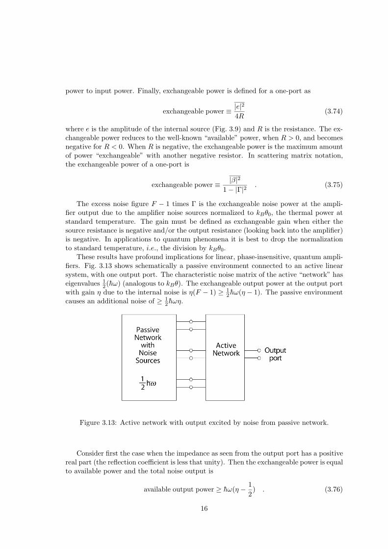
The excess noise figure F − 1 times Γ is the exchangeable noise power at the ampli-fier output due to the amplifier noise sources normalized to kBθ0, the thermal power atstandard temperature. The gain must be defined as exchangeable gain when either thesource resistance is negative and/or the output resistance (looking back into the amplifier)is negative. In applications to quantum phenomena it is best to drop the normalizationto standard temperature, i.e., the division by kBθ0.
These results have profound implications for linear, phase-insensitive, quantum ampli-fiers. Fig. 3.13 shows schematically a passive environment connected to an active linearsystem, with one output port. The characteristic noise matrix of the active “network” haseigenvalues 1
2(h̄ω) (analogous to kBθ). The exchangeable output power at the output portwith gain η due to the internal noise is η(F − 1) ≥ 1
2 h̄ω(η − 1). The passive environmentcauses an additional noise of ≥ 1
2 h̄ωη.
Figure 3.13: Active network with output excited by noise from passive network.
Consider first the case when the impedance as seen from the output port has a positivereal part (the reflection coefficient is less that unity). Then the exchangeable power is equalto available power and the total noise output is
available output power ≥ h̄ω(η − 12) . (3.76)
16
When the gain is unity, the output noise power is equal to that of the zero-point fluctu-ations. When the gain is much larger than unity, the output noise power referred to theinput by division by the gain η is h̄ω. This is in agreement with the results of Arthursand Kelly[9]. A large gain allows a simulataneous measurement of the noncommutingobservables a1 and a2 and, thus, must at least double the uncertainty product, i.e., atleast double the noise.
3.6.4 Phase sensitive system
If a quantum system is characterized by the phase sensitive scattering coefficients:
b1 = Γ1a1 + β1 , (3.77)b2 = Γ2a1 + β2 ,
the commutator bracket of the output wave is given by
[b1, b2] = Γ1Γ2 [a1, a2] + [β1, β2] . (3.78)
Since [a1, a2] = [b1, b2] = i2 h̄ω, we obtain the new commutator bracket for the noise:
[β1, β2] = (1− Γ1Γ2)12h̄ω . (3.79)
One then immediately note that if Γ1 = 1/Γ2 is satisfied, the commutator bracket (3.79)disppears and such a system does not need to add the quantum noise on the ampli-fied/deamplified signal. When Γ1 = 1/Γ2 > 1, the in-phase amplitude a1 is amplifiedwhile the quadrature amplitude a2 is deamplified. The noise figure F for such a phasesentive amplifier is 1(0dB), in contrast to the minimum noise figure of 2 (3dB) of a phaseinsensitive amplifier [15]. We will see in chapter 10 and chapter 11 that a laser amplifierand degenerate parametric amplifier as a respective example of such phase insensitive andphase sensitive amplifiers.
17
Bibliography
[1] H. A. Haus and J. A. Mullen, Phys. Rev., 128, 2407 (1962).