www.ti.com SNLS046E –FEBRUARY 2000–REVISED APRIL 2013
CLC020 SMPTE 259M Digital Video Serializer with Integrated Cable DriverCheck for Samples: CLC020
1FEATURES DESCRIPTIONThe CLC020 SMPTE 259M Digital Video Serializer
2• SMPTE 259M Serial Digital Video Standardwith Integrated Cable Driver is a monolithic integratedCompliantcircuit that encodes, serializes and transmits bit-
• No External Serial Data Rate Setting or VCO parallel digital data conforming to SMPTE 125M andFiltering Components Required (1)
SMPTE 267M component video and SMPTE 244Mcomposite video standards. The CLC020 can also• Built-In Self-Test (BIST) and Video Test Patternserialize other 8 or 10-bit parallel data. The CLC020Generator (TPG) with 16 Internal Patterns (1)
operates at data rates from below 100 Mbps to over• Supports All NTSC and PAL Standard400 Mbps. The serial data clock frequency is
Component and Composite Serial Video Data internally generated and requires no externalRates frequency setting components, trimming or filtering*.
• HCMOS/TTL-Compatible Data and Control Functions performed by the CLC020 include: parallel-to-serial data conversion, data encoding using theInputs and Outputspolynomial (X9+X4+1), data format conversion from• 75Ω ECL-Compatible, Differential, Serial Cable-NRZ to NRZI, parallel data clock frequencyDriver Outputsmultiplication and encoding with the serial data, and
• Fast VCO Lock Time: <75 µs coaxial cable driving. Input for sync (TRS) detectiondisabling and a PLL lock detect output are provided.• Single +5V TTL or −5V ECL Supply OperationThe CLC020 has an exclusive built-in self-test (BIST)• Low Power: 235 mW Typicaland video test pattern generator (TPG) with 4
• 28-Lead PLCC Package component video test patterns, reference black, PLL• Commercial Temperature Range 0°C to +70°C and EQ pathologicals and modified colour bars, in 4:3
and 16:9 raster and both NTSC and PAL formats*.Separate power pins for the output driver, VCO andAPPLICATIONSthe digital logic improve power supply rejection,
• SMPTE 259M Parallel-to-Serial Digital Video output jitter and noise performance.Interfaces for:
The CLC020 is the ideal complement to the– Video Cameras CLC011B SMPTE 259M Serial Digital Video– VTRs Decoder, CLC014 Active Cable Equalizer, CLC016
Data Retiming PLL (clock-data separator), CLC018– Telecines8X8 Digital Crosspoint Switch and CLC006 or– Video Test Pattern Generators and DigitalCLC007 Cable Drivers, for a complete parallel-serial-Video Test Equipment parallel, high-speed data processing and
• Non-SMPTE Video Applications transmission system.• Other High Data Rate Parallel/Serial Video and The CLC020 is powered from a single 5V supply.
Data Systems Power dissipation is typically 235 mW including two75Ω back-matched output loads. The device ispackaged in a JEDEC 28-lead PLCC.
(1) Patents Applications Made or Pending.
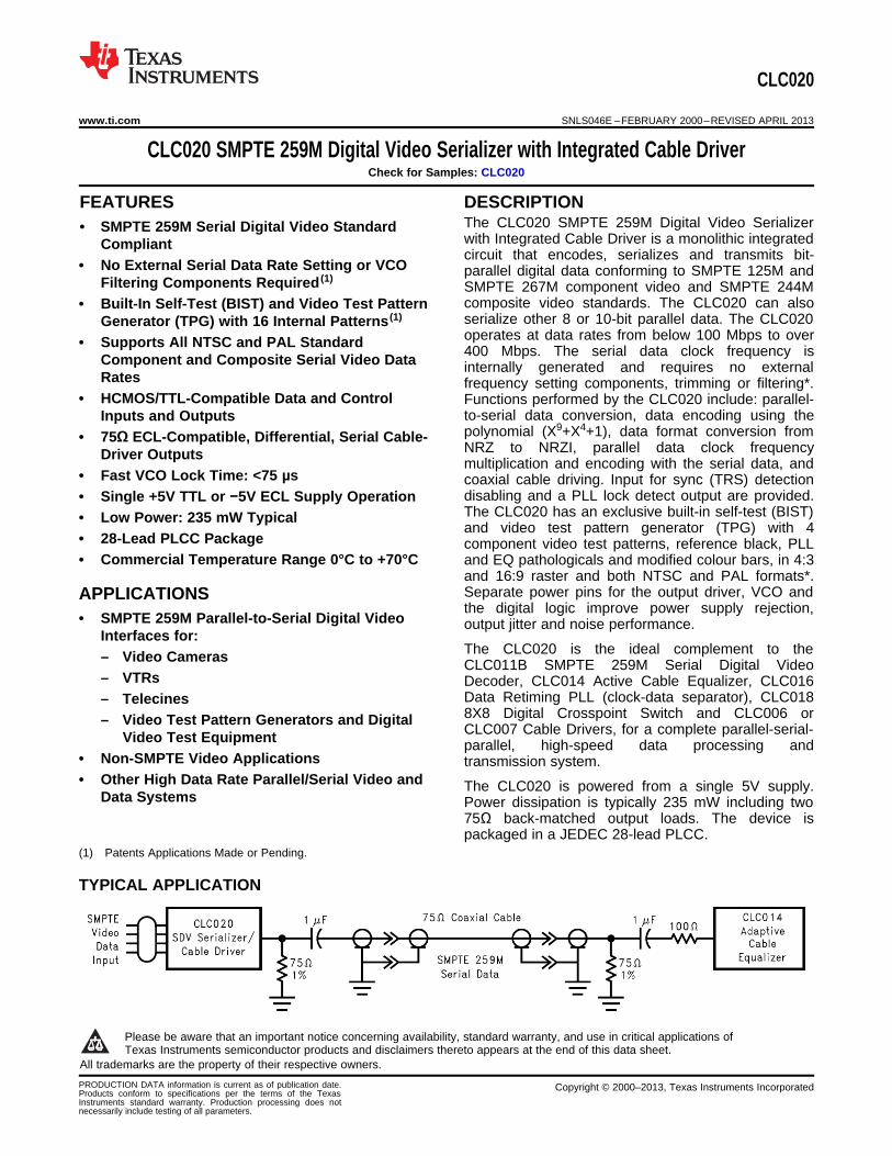
TYPICAL APPLICATION
1
Please be aware that an important notice concerning availability, standard warranty, and use in critical applications ofTexas Instruments semiconductor products and disclaimers thereto appears at the end of this data sheet.
2All trademarks are the property of their respective owners.
www.ti.com SNLS046E –FEBRUARY 2000–REVISED APRIL 2013
These devices have limited built-in ESD protection. The leads should be shorted together or the device placed in conductive foamduring storage or handling to prevent electrostatic damage to the MOS gates.
ABSOLUTE MAXIMUM RATINGS (1) (2)
Supply Voltage (VDD−VSS) 6.0V
CMOS/TTL Input Voltage (VI) −0.5V to (VDD + 0.5V)
CMOS/TTL Output Voltage (VO) −0.5V to (VDD + 0.5V)
CMOS/TTL Input Current (single input) VI = VSS −0.5V −5 mA
(1) Absolute Maximum Ratings are those parameter values beyond which the life and operation of the device cannot be ensured. Thestating herein of these maximums shall not be construed to imply that the device can or should be operated at or beyond these values.The table of Electrical Characteristics specifies acceptable device operating conditions.
(2) If Military/Aerospace specified devices are required, please contact the Texas Instruments Sales Office/ Distributors for availability andspecifications.
RECOMMENDED OPERATING CONDITIONSSupply Voltage (VDD−VSS) 5.0V ±10%
PCLK = 27 MHz, See Figure 3,NTSC Colour Bar Pattern
(1) Current flow into device pins is defined as positive. Current flow out of device pins is defined as negative. All voltages are statedreferenced to VSS = 0V.
(2) Typical values are stated for VDD = +5.0V and TA = +25°C.
AC ELECTRICAL CHARACTERISTICSOver Supply Voltage and Operating Temperature ranges, unless otherwise specified. (1)
Symbol Parameter Conditions Reference Min Typ Max Units
BRSDO Serial data rate RL = 75Ω, AC coupled (2) SDO, SDO 100 400 Mbps
FPCLK Reference Clock PCLK 10 40 MHzInput Frequency
Reference Clock Duty PCLK 45 50 55 %Cycle
tr, tf Rise time, Fall time 10%–90% DN, PCLK 1.0 1.5 3.0 ns
tj Serial output jitter 270 Mbps (3), See Figure 3 220 psP-P
tjit Serial output jitter See (4) (2) 100 200 psP-PSDO, SDO
tr, tf Rise time, Fall time 20%–80% (2) (4) 500 800 1500 ps
Output overshoot 1 %
tLOCK Lock time 270 Mbps (2) (5) 75 µs
tSU Setup time See Figure 4 DN to PCLK 3 2 ns
tHLD Hold time See Figure 4 DN from PCLK 1.5 1 ns
LGEN Output inductance See (4) 6 nHSDO, SDO
RGEN Output resistance See (4) 25k Ω
(1) Typical values are stated for VDD = +5.0V and TA = +25°C.(2) RL = 75Ω, AC-coupled @ 270 Mbps, RREF = 1.69 kΩ 1%, See TEST LOADS and Figure 3.(3) CLC020 mounted in the SD020EVK board, configured in BIST mode (NTSC color bars) with PCLK = 27MHz derived from Tektronix
TG2000 black-burst reference. Timing jitter measured with Tektronix VM700T using jitter measurement FFT mode, frame rate, 1kHzfilter bandwidth, Hanning window.
(4) Specification is ensured by design.(5) Measured from rising-edge of first PCLK cycle until Lock Detect output goes high (true).
SNLS046E –FEBRUARY 2000–REVISED APRIL 2013 www.ti.com
TIMING DIAGRAM
Figure 4. Setup and Hold Timing
DEVICE OPERATION
The CLC020 SMPTE 259M Digital Video Serializer is used in digital video signal origination and processingequipment: cameras, video tape recorders, telecines, video test equipment and others. It converts parallelcomponent or composite digital video signals into serial format. Logic levels within this equipment are normallyTTL-compatible as produced by CMOS or bipolar logic devices. The encoder outputs ECL-compatible serialdigital video (SDV) signals conforming to SMPTE 259M-1997. The CLC020 operates at all standard SMPTE andITU-R parallel data rates.
VIDEO DATA PROCESSING CIRCUITS
The input data register accepts 8 or 10-bit parallel data and clock signals having CMOS/TTL-compatible signallevels. Parallel data may conform to any of several standards: SMPTE 125M, SMPTE 267M, SMPTE 244M orITU-R BT.601. If data is 8-bit, it is converted to a 10-bit representation according to the type of data being input:component 4:2:2 per SMPTE 259M paragraph 7.1.1, composite NTSC per paragraph 8.1.1 or composite PALper paragraph 9.1.1. Output from this register feeds the SMPTE polynomial generator/serializer and syncdetector. All CMOS inputs including the PCLK input have internal pull-down devices.
The sync detector or TRS character detector accepts data from the input register. The detection function iscontrolled by Sync Detect Enable, a low-true, TTL-compatible, external signal. Synchronization words, the timingreference signals (TRS), start-of-active-video (SAV) and end-of-active-video (EAV) are defined in SMPTE 125M-1995 and 244M. The sync detector supplies control signals to the SMPTE polynomial generator that identify thepresence of valid video data. The sync detector performs input TRS character LSB-clipping as prescribed in ITU-R-BT.601. LSB-clipping causes all TRS characters with a value between 000h and 003h to be forced to 000hand all TRS characters with a value between 3FCh and 3FFh to be forced to 3FFh. Clipping is done prior toencoding.
The SMPTE polynomial generator accepts the parallel video data and encodes it using the polynomial X9+X4+1as specified in SMPTE 259M–1997, paragraph 5 and Annex C. The scrambled data is then serialized for output.
The NRZ-to-NRZI converter accepts serial NRZ data from the SMPTE polynomial genertor and converts it toNRZI using the polynomial X + 1 per SMPTE 259M–1997, paragraph 5.2 and Annex C. The transmission bitorder is LSB first, per paragraph 6. The converter's output feeds the output driver amplifier.
PHASE-LOCKED LOOP AND VCO
The phase-locked loop (PLL) system generates the output serial data clock at 10× the parallel data clockfrequency. This system consists of a VCO, divider chain, phase-frequency detector and internal loop filter. TheVCO free-running frequency is internally set. The PLL automatically generates the appropriate frequency for theserial clock rate using the parallel data clock (PCLK) frequency as its reference. Loop filtering is internal to theCLC020. The VCO has separate VSSO and VDDO power supply feeds, pins 15 and 16, which may be suppliedpower independently via an external low-pass filter, if desired. The PLL acquisition (lock) time is less than 75 µs@ 270 Mbps.
www.ti.com SNLS046E –FEBRUARY 2000–REVISED APRIL 2013
LOCK DETECT
The Lock Detect output of the phase-frequency detector indicates the PLL lock condition. It is a logic HIGHwhen the loop is locked. The output is CMOS/TTL-compatible and is suitable for driving other CMOS devices ora LED indicator.
SERIAL DATA OUTPUT BUFFER
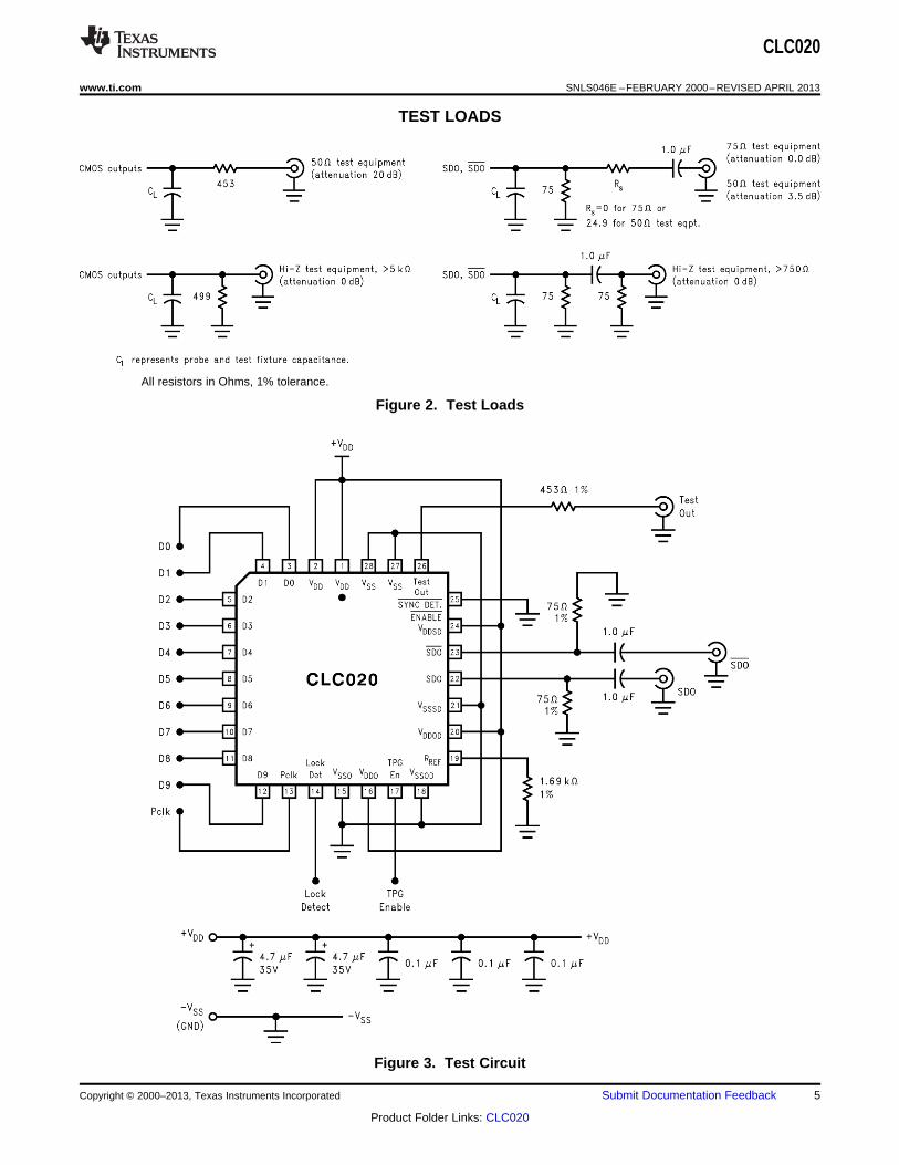
The current-mode serial data outputs provide low-skew complimentary or differential signals. The output bufferdesign can drive 75Ω coaxial cables (AC-coupled) or 10k/100k ECL/PECL-compatible devices (DC-coupled).Output levels are 800 mVP-P ±10% into 75Ω AC-coupled, back-matched loads. The output level is 400 mVP-P±10% when DC-coupled into 75Ω (See APPLICATION INFORMATION for details). The 75Ω resistors connectedto the SDO outputs are back-matching resistors. No series back-matching resistors should be used. SDO outputlevels are controlled by the value of RREF connected to pin 19. The value of RREF is normally 1.69 kΩ, ±1%. Theoutput buffer is static when the device is in an out-of-lock condition. Separate VSSSD and VDDSD power feeds, pins21 and 24, are provided for the serial output driver.
POWER-ON RESET
The CLC020 has an internally controlled, automatic, power-on reset circuit. This circuit clears TRS detectioncircuitry, all latches, registers, counters and polynomial generators and disables the serial output. The SDOoutputs are tri-stated during power-on reset. The part will remain in the reset condition until the parallel inputclock is applied.
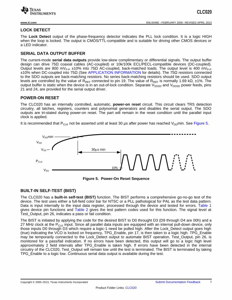
It is recommended that PCLK not be asserted until at least 30 µs after power has reached VDDmin. See Figure 5.
Figure 5. Power-On Reset Sequence
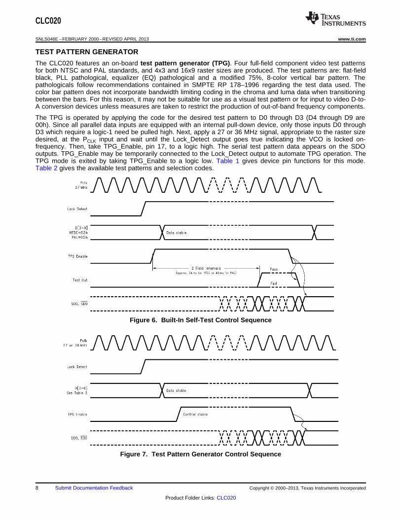
BUILT-IN SELF-TEST (BIST)
The CLC020 has a built-in self-test (BIST) function. The BIST performs a comprehensive go-no-go test of thedevice. The test uses either a full-field color bar for NTSC or a PLL pathological for PAL as the test data pattern.Data is input internally to the input data register, processed through the device and tested for errors. Table 1gives device pin functions and Table 2 gives the test pattern codes used for this function. The signal level atTest_Output, pin 26, indicates a pass or fail condition.
The BIST is initiated by applying the code for the desired BIST to D0 throught D3 (D9 through D4 are 00h) and a27 MHz clock at the PCLK input. Since all parallel data inputs are equipped with an internal pull-down device, onlythose inputs D0 through D3 which require a logic-1 need be pulled high. After the Lock_Detect output goes high(true) indicating the VCO is locked on frequency, TPG_Enable, pin 17, is then taken to a logic high. TPG_Enablemay be temporarily connected to the Lock_Detect output to automate BIST operation. Test_Output, pin 26, ismonitored for a pass/fail indication. If no errors have been detected, this output will go to a logic high levelapproximately 2 field intervals after TPG_Enable is taken high. If errors have been detected in the internalcircuitry of the CLC020, Test_Output will remain low until the test is terminated. The BIST is terminated by takingTPG_Enable to a logic low. Continuous serial data output is available during the test.
SNLS046E –FEBRUARY 2000–REVISED APRIL 2013 www.ti.com
TEST PATTERN GENERATOR
The CLC020 features an on-board test pattern generator (TPG). Four full-field component video test patternsfor both NTSC and PAL standards, and 4x3 and 16x9 raster sizes are produced. The test patterns are: flat-fieldblack, PLL pathological, equalizer (EQ) pathological and a modified 75%, 8-color vertical bar pattern. Thepathologicals follow recommendations contained in SMPTE RP 178–1996 regarding the test data used. Thecolor bar pattern does not incorporate bandwidth limiting coding in the chroma and luma data when transitioningbetween the bars. For this reason, it may not be suitable for use as a visual test pattern or for input to video D-to-A conversion devices unless measures are taken to restrict the production of out-of-band frequency components.
The TPG is operated by applying the code for the desired test pattern to D0 through D3 (D4 through D9 are00h). Since all parallel data inputs are equipped with an internal pull-down device, only those inputs D0 throughD3 which require a logic-1 need be pulled high. Next, apply a 27 or 36 MHz signal, appropriate to the raster sizedesired, at the PCLK input and wait until the Lock_Detect output goes true indicating the VCO is locked on-frequency. Then, take TPG_Enable, pin 17, to a logic high. The serial test pattern data appears on the SDOoutputs. TPG_Enable may be temporarily connected to the Lock_Detect output to automate TPG operation. TheTPG mode is exited by taking TPG_Enable to a logic low. Table 1 gives device pin functions for this mode.Table 2 gives the available test patterns and selection codes.
www.ti.com SNLS046E –FEBRUARY 2000–REVISED APRIL 2013
APPLICATION INFORMATION
A typical application circuit for the CLC020 is shown in Figure 8. This circuit demonstrates the capabilities of theCLC020 and allows its evaluation in a variety of configurations. An assembled demonstration board with morecomprehensive evaluation options is available, part number SD020EVK. The board may be ordered through anyof Texas Instruments's sales offices. Complete circuit board layouts and schematics, for the SD020EVK areavailable on Texas Instruments' WEB site in the application information for this device.
APPLICATION CIRCUIT
Figure 8. Typical Application Circuit
Several different input and output drive and loading options can be constructed on the SD020EVK applicationcircuit board, Figure 9. Pin headers are provided for input cabling and control signal access. The appropriatevalue resistor packs, 220 and 330Ω for TTL or 50Ω for signal sources requiring such loading, should be installedat RP1-4 before applying input signals.
The board's outputs may be DC interfaced to PECL inputs by first installing 124Ω resistors at R1B and R2B,changing R1A and R2A to 187Ω and replacing C1 and C2 with short circuits. The PECL inputs should be directlyconnected to J1 and J2 without cabling. If 75Ω cabling is used to connect the CLC020 to the PECL inputs, thevoltage dividers used on the CLC020 outputs must be removed and re-installed on the circuit board where thePECL device is mounted. This will provide correct termination for the cable and biasing for both the CLC020'soutputs and the PECL inputs. It is most important to note that a 75Ω or equivalent DC loading (measured withrespect to the negative supply rail) must always be installed at both of the CLC020's SDO outputs to obtainproper signal levels from device. When using 75Ω Thevenin-equivalent load circuits, the DC bias applied to theSDO outputs should not exceed +3V with respect to the negative supply rail. Serial output levels should bereduced to 400 mVp-p by changing RREF to 3.4 kΩ.
SNLS046E –FEBRUARY 2000–REVISED APRIL 2013 www.ti.com
The Test Out output is intended for monitoring by equipment presenting high impedance loading (>500Ω). Whenmonitoring the Lock Detect output, the attached monitoring circuit should present a DC resistance greater than 5kΩ so that Lock Detect indicator operation is not affected.
Connect LOCK DETECT to TPG ENABLE for test pattern generator function.Remove RP1 & RP3 and replace RP2 & RP4 with 50Ω resistor packs for coax interfacing.Install RP1-4 when using ribbon cable for input interfacing.This board is designed for use with TTL power supplies only.For optional ECL compatible load: R1A = R2A = 187; R1B = R2B = 124.All resistances & impedances in Ohms. Values with 3 significant digits are 1%; with 2 digits 5%.
Figure 9. SD020EVK Schematic Diagram
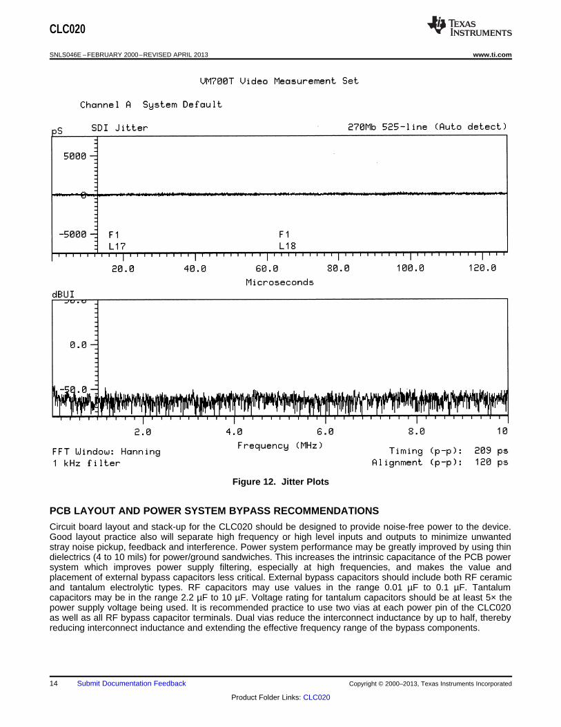
MEASURING JITTER
The test method used to obtain the timing jitter value given in the AC Electrical Specification table is based onprocedures and equipment described in SMPTE RP 192-1996. The recommended practice discusses severalmethods and indicator devices. An FFT method performed by standard video test equipment was used to obtainthe data given in this data sheet. As such, the jitter characteristics (or jitter floor) of the measurement equipment,particularly the measurement analyzer, become integral to the resulting jitter value. The method and equipmentwere chosen so that the test can be easily duplicated by the design engineer using most standard digital videotest equipment. In so doing, similar results should be achieved. The intrinsic jitter floor of the CLC020's PLL isapproximately 25% of the typical jitter given in the electrical specifications. In production, device jitter ismeasured on automatic IC test equipment (ATE) using a different method compatible with that equipment. Jittermeasured using this ATE yields values approximately 50% of those obtained using the video test equipment.
www.ti.com SNLS046E –FEBRUARY 2000–REVISED APRIL 2013
The jitter test setup used to obtain values quoted in the data sheet consists of:• Texas Instruments SD020EVK, CLC020 evaluation kit• Tektronix TG2000 signal generation platform with DVG1 option• Tektronix VM700T Option 1S Video Measurement Set• Tektronix TDS 794D, Option C2 oscilloscope• Tektronix P6339A passive probe• 75 Ohm coaxial cable, 3ft., Belden 8281 or RG59 (2 required)• ECL-to-TTL/CMOS level converter/amplifier, Figure 11
Apply the black-burst reference clock from the TG2000 signal generator's BG1 module 27MHz clock output to thelevel converter input. The clock amplitude converter schematic is shown in Figure 10. Adjust the input biascontrol to give a 50% duty cycle output as measured on the oscilloscope/probe system. Connect the leveltranslator to the SD020EVK board, connector P1, PCLK pins (the outer-most row of pins is ground). Configure theSD020EVK to operate in the NTSC colour bars, BIST mode. Configure the VM700T to make the jittermeasurement in the jitter FFT mode at the frame rate with 1kHz filter bandwidth and Hanning window. Configurethe setup as shown in Figure 10. Switch the test equipment on (from standby mode) and allow all equipmenttemperatures stabilize per manufacturer's recommendation. Measure the jitter value after allowing theinstrument's reading to stabilize (about 1 minute). Consult the VM700T Video Measurement Set Option 1S SerialDigital Measurements User Manual (document number 071-0074-00) for details of equipment operation.
The VM700T measurement system's jitter floor specification at 270Mbps is given as 200ps ±20% (100ps ±5%typical) of actual components from 50Hz to 1MHz and 200ps +60%, -30% of actual components from 1MHz to10MHz. To obtain the actual residual jitter of the CLC020, a root-sum-square adjustment of the jitter readingmust be made to compensate for the measurement system's jitter floor specification. For example, if the jitterreading is 250ps, the CLC020 residual jitter is the square root of (2502 − 2002) = 150ps. The accuracy limits ofthe reading as given above apply.
SNLS046E –FEBRUARY 2000–REVISED APRIL 2013 www.ti.com
Figure 12. Jitter Plots
PCB LAYOUT AND POWER SYSTEM BYPASS RECOMMENDATIONS
Circuit board layout and stack-up for the CLC020 should be designed to provide noise-free power to the device.Good layout practice also will separate high frequency or high level inputs and outputs to minimize unwantedstray noise pickup, feedback and interference. Power system performance may be greatly improved by using thindielectrics (4 to 10 mils) for power/ground sandwiches. This increases the intrinsic capacitance of the PCB powersystem which improves power supply filtering, especially at high frequencies, and makes the value andplacement of external bypass capacitors less critical. External bypass capacitors should include both RF ceramicand tantalum electrolytic types. RF capacitors may use values in the range 0.01 µF to 0.1 µF. Tantalumcapacitors may be in the range 2.2 µF to 10 µF. Voltage rating for tantalum capacitors should be at least 5× thepower supply voltage being used. It is recommended practice to use two vias at each power pin of the CLC020as well as all RF bypass capacitor terminals. Dual vias reduce the interconnect inductance by up to half, therebyreducing interconnect inductance and extending the effective frequency range of the bypass components.
www.ti.com SNLS046E –FEBRUARY 2000–REVISED APRIL 2013
The outer layers of the PCB may be flooded with additional VSS (ground) plane. These planes will improveshielding and isolation as well as increase the intrinsic capacitance of the power supply plane system. Naturally,to be effective, these planes must be tied to the VSS power supply plane at frequent intervals with vias. Frequentvia placement also improves signal integrity on signal transmission lines by providing short paths for imagecurrents which reduces signal distortion. The planes should be pulled back from all transmission lines andcomponent mounting pads a distance equal to the width of the widest transmission line or the thickness of thedielectric separating the transmission line from the internal power or ground plane(s) whichever is greater. Doingso minimizes effects on transmission line impedances and reduces unwanted parasitic capacitances atcomponent mounting pads.
In especially noisy power supply environments, such as is often the case when using switching power supplies,separate filtering may be used at the CLC020's VCO and output driver power pins. The CLC020 was designedfor this situation. The digital section, VCO and output driver power supply feeds are independent (see PINDESCRIPTIONS table and Pinout Drawing for details). Supply filtering may take the form of L-section or pi-section, L-C filters in series with these VDD inputs. Such filters are available in a single package from severalmanufacturers. Despite being independent feeds, all device power supplies should be applied simultaneously asfrom a common source. The CLC020 is free from power supply latch-up caused by circuit-induced delaysbetween the device's three separate power feed systems.
REPLACING THE GENNUM GS9022
The CLC020 is form-fit-function compatible with the Gennum GS9022. The CLC020 can improve theperformance of GS9022 applications using the existing PCB layout with the removal of certain components orchanges to component values. New layouts using the CLC020 will benefit from the greatly reduced ancilliarycomponent count and more compact layout.
The CLC020 does not require external VCO filtering components. The external VCO filtering components at pin17 of the GS9022 may remain connected to the CLC020 without complications. It is suggested that these beremoved from the circuit board. The CLC020 uses pin 17 for its test pattern generator enable function. You willfind the TPG function very useful when you make this change.
Remove the COSC capacitor used by the GS9022 at pin 26. The CLC020 uses pin 26 as the BIST pass/failindicator output. You may attach a LED as an indicator to this pin, if desired. LED current should be limited to 10mA maximum. The same LED type and current limiting resistor shown in Figure 9 at the Lock Detect output maybe used for this indicator function.
Remove any capacitor attached to pin 19. A capacitor attached to pin 19 will cause distortion of the output VOHlevel. The former data rate setting resistor, RVCO, at pin 19 now functions as the output level setting resistor,RREF. It must be changed to a 1.69 kΩ, 1% value for correct output level setting.
The input series resistors and the PCLK risetime filter capacitor used with the GS9022 are not needed for theCLC020. These components should be removed from the circuit board and the resistors replaced by shortcircuits (0Ω resistors). These series resistors will increase input signal rise and fall times if left on the board.
The CLC020 has current-mode serial cable driver outputs. These outputs have very high internal generatorresistance as one would expect of a current source. Though these current-mode outputs can produce theequivalent drive voltages into the load, it is necessary to change and simplify the typical GS9022 output circuitnormally recommended for that device. The output load resistors at pins 22 and 23 must be changed to 75Ω, 1%values. These resistors become the back-matching loads across which the CLC020's outputs develop drivevoltage. The series back-matching resistors used on the GS9022 should be removed and replaced with shortcircuits. The risetime compensating capacitors across these resistors should be removed.
Pin 28 on the CLC020 is VSS and must be connected to the negative supply or ground. On layouts designed tomount the GS9022, the series R-C network connected to this pin should be replaced by short circuits (0Ωresistors). The pull-up resistor connected to the Lock Detect output, pin 14, should be removed. It may bereplaced by a LED and current limiting resistor connected to VSS if a visual lock indicator is desired.
The CLC020 has an internal pull-down at the Sync Detect Enable input and may be left unconnected in SMPTEvideo-only applications.
The CLC020 has independent power supply pins for the VCO, VSSO, pin 15 and VDDO, pin 16. The CLC020 hasan output driver negative supply, VSSSD, at pin 21. The output driver positive supply, VDDSD, is pin 24 (as on theGS9022). On new layouts, additional power supply filtering may be added at these pins, if desired.
SNLS046E –FEBRUARY 2000–REVISED APRIL 2013 www.ti.com
REVISION HISTORY
Changes from Revision D (April 2013) to Revision E Page
• Changed layout of National Data Sheet to TI format .......................................................................................................... 15
CLC020BCQ/NOPB ACTIVE PLCC FN 28 35 Green (RoHS& no Sb/Br)
SN Level-2A-245C-4WEEK
0 to 70 CLC020BCQ
(1) The marketing status values are defined as follows:ACTIVE: Product device recommended for new designs.LIFEBUY: TI has announced that the device will be discontinued, and a lifetime-buy period is in effect.NRND: Not recommended for new designs. Device is in production to support existing customers, but TI does not recommend using this part in a new design.PREVIEW: Device has been announced but is not in production. Samples may or may not be available.OBSOLETE: TI has discontinued the production of the device.
(2) Eco Plan - The planned eco-friendly classification: Pb-Free (RoHS), Pb-Free (RoHS Exempt), or Green (RoHS & no Sb/Br) - please check http://www.ti.com/productcontent for the latest availabilityinformation and additional product content details.TBD: The Pb-Free/Green conversion plan has not been defined.Pb-Free (RoHS): TI's terms "Lead-Free" or "Pb-Free" mean semiconductor products that are compatible with the current RoHS requirements for all 6 substances, including the requirement thatlead not exceed 0.1% by weight in homogeneous materials. Where designed to be soldered at high temperatures, TI Pb-Free products are suitable for use in specified lead-free processes.Pb-Free (RoHS Exempt): This component has a RoHS exemption for either 1) lead-based flip-chip solder bumps used between the die and package, or 2) lead-based die adhesive used betweenthe die and leadframe. The component is otherwise considered Pb-Free (RoHS compatible) as defined above.Green (RoHS & no Sb/Br): TI defines "Green" to mean Pb-Free (RoHS compatible), and free of Bromine (Br) and Antimony (Sb) based flame retardants (Br or Sb do not exceed 0.1% by weightin homogeneous material)
(3) MSL, Peak Temp. -- The Moisture Sensitivity Level rating according to the JEDEC industry standard classifications, and peak solder temperature.
(4) There may be additional marking, which relates to the logo, the lot trace code information, or the environmental category on the device.
(5) Multiple Device Markings will be inside parentheses. Only one Device Marking contained in parentheses and separated by a "~" will appear on a device. If a line is indented then it is a continuationof the previous line and the two combined represent the entire Device Marking for that device.
Important Information and Disclaimer:The information provided on this page represents TI's knowledge and belief as of the date that it is provided. TI bases its knowledge and belief on informationprovided by third parties, and makes no representation or warranty as to the accuracy of such information. Efforts are underway to better integrate information from third parties. TI has taken andcontinues to take reasonable steps to provide representative and accurate information but may not have conducted destructive testing or chemical analysis on incoming materials and chemicals.TI and TI suppliers consider certain information to be proprietary, and thus CAS numbers and other limited information may not be available for release.
In no event shall TI's liability arising out of such information exceed the total purchase price of the TI part(s) at issue in this document sold by TI to Customer on an annual basis.
NOTES: A. All linear dimensions are in inches (millimeters).B. This drawing is subject to change without notice.C. Falls within JEDEC MS-018
IMPORTANT NOTICE
Texas Instruments Incorporated and its subsidiaries (TI) reserve the right to make corrections, enhancements, improvements and otherchanges to its semiconductor products and services per JESD46, latest issue, and to discontinue any product or service per JESD48, latestissue. Buyers should obtain the latest relevant information before placing orders and should verify that such information is current andcomplete. All semiconductor products (also referred to herein as “components”) are sold subject to TI’s terms and conditions of salesupplied at the time of order acknowledgment.
TI warrants performance of its components to the specifications applicable at the time of sale, in accordance with the warranty in TI’s termsand conditions of sale of semiconductor products. Testing and other quality control techniques are used to the extent TI deems necessaryto support this warranty. Except where mandated by applicable law, testing of all parameters of each component is not necessarilyperformed.
TI assumes no liability for applications assistance or the design of Buyers’ products. Buyers are responsible for their products andapplications using TI components. To minimize the risks associated with Buyers’ products and applications, Buyers should provideadequate design and operating safeguards.
TI does not warrant or represent that any license, either express or implied, is granted under any patent right, copyright, mask work right, orother intellectual property right relating to any combination, machine, or process in which TI components or services are used. Informationpublished by TI regarding third-party products or services does not constitute a license to use such products or services or a warranty orendorsement thereof. Use of such information may require a license from a third party under the patents or other intellectual property of thethird party, or a license from TI under the patents or other intellectual property of TI.
Reproduction of significant portions of TI information in TI data books or data sheets is permissible only if reproduction is without alterationand is accompanied by all associated warranties, conditions, limitations, and notices. TI is not responsible or liable for such altereddocumentation. Information of third parties may be subject to additional restrictions.
Resale of TI components or services with statements different from or beyond the parameters stated by TI for that component or servicevoids all express and any implied warranties for the associated TI component or service and is an unfair and deceptive business practice.TI is not responsible or liable for any such statements.
Buyer acknowledges and agrees that it is solely responsible for compliance with all legal, regulatory and safety-related requirementsconcerning its products, and any use of TI components in its applications, notwithstanding any applications-related information or supportthat may be provided by TI. Buyer represents and agrees that it has all the necessary expertise to create and implement safeguards whichanticipate dangerous consequences of failures, monitor failures and their consequences, lessen the likelihood of failures that might causeharm and take appropriate remedial actions. Buyer will fully indemnify TI and its representatives against any damages arising out of the useof any TI components in safety-critical applications.
In some cases, TI components may be promoted specifically to facilitate safety-related applications. With such components, TI’s goal is tohelp enable customers to design and create their own end-product solutions that meet applicable functional safety standards andrequirements. Nonetheless, such components are subject to these terms.
No TI components are authorized for use in FDA Class III (or similar life-critical medical equipment) unless authorized officers of the partieshave executed a special agreement specifically governing such use.
Only those TI components which TI has specifically designated as military grade or “enhanced plastic” are designed and intended for use inmilitary/aerospace applications or environments. Buyer acknowledges and agrees that any military or aerospace use of TI componentswhich have not been so designated is solely at the Buyer's risk, and that Buyer is solely responsible for compliance with all legal andregulatory requirements in connection with such use.
TI has specifically designated certain components as meeting ISO/TS16949 requirements, mainly for automotive use. In any case of use ofnon-designated products, TI will not be responsible for any failure to meet ISO/TS16949.
Products Applications
Audio www.ti.com/audio Automotive and Transportation www.ti.com/automotive
Amplifiers amplifier.ti.com Communications and Telecom www.ti.com/communications
Data Converters dataconverter.ti.com Computers and Peripherals www.ti.com/computers