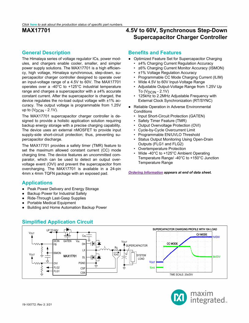
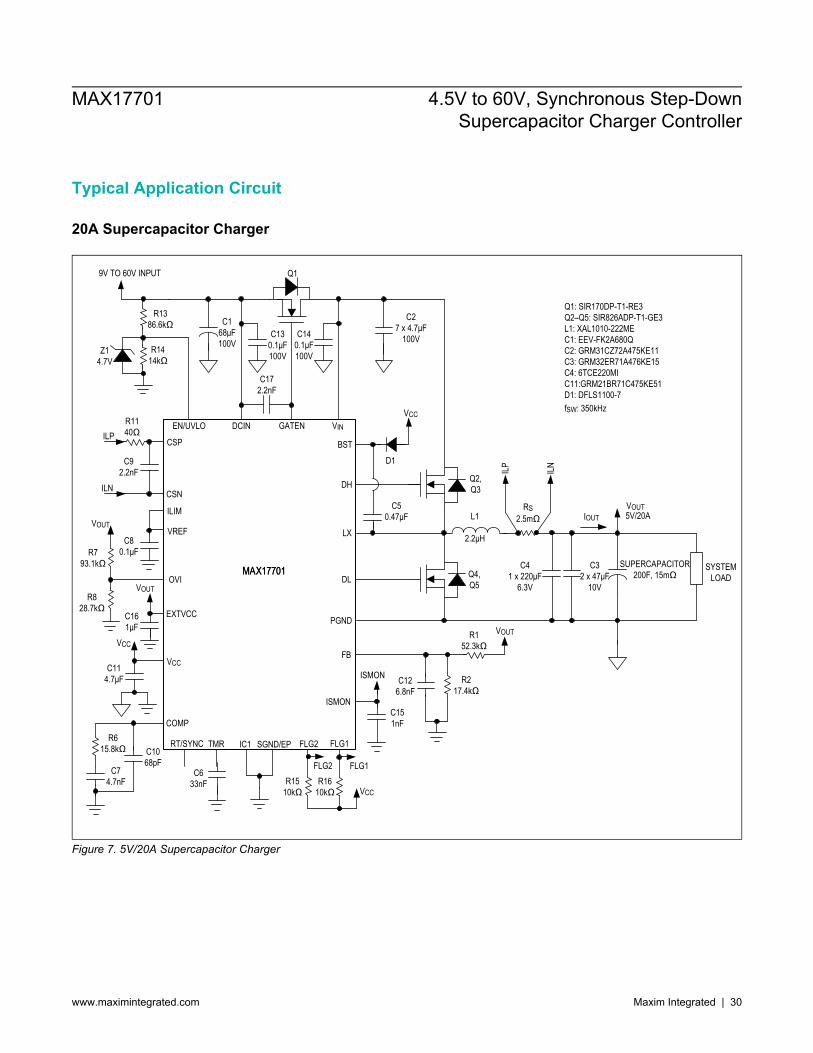
General Description The Himalaya series of voltage regulator ICs, power mod- ules, and chargers enable cooler, smaller, and simpler power supply solutions. The MAX17701 is a high efficien- cy, high voltage, Himalaya synchronous, step-down, su- percapacitor charger controller designed to operate over an input-voltage range of a 4.5V to 60V. The MAX17701 operates over a -40°C to +125°C industrial temperature range and charges a supercapacitor with a ±4% accurate constant current. After the supercapacitor is charged, the device regulates the no-load output voltage with ±1% ac- curacy. The output voltage is programmable from 1.25V up to (V DCIN - 2.1V). The MAX17701 supercapacitor charger controller is de- signed to provide a holistic application solution requiring backup energy storage with a precise charging capability. The device uses an external nMOSFET to provide input supply-side short-circuit protection; thus, preventing su- percapacitor discharge. The MAX17701 provides a safety timer (TMR) feature to set the maximum allowed constant current (CC) mode charging time. The device features an uncommitted com- parator, which can be used to detect an output over- voltage event (OVI) and prevent the supercapacitor from overcharging. The MAX17701 is available in a 24-pin 4mm x 4mm TQFN package with an exposed pad. Applications ● Peak Power Delivery and Energy Storage ● Backup Power for Industrial Safety ● Ride-Through Last-Gasp Supplies ● Portable Medical Equipment ● Building and Home Automation Backup Power Benefits and Features ● Optimized Feature Set for Supercapacitor Charging • ±4% Charging Current Regulation Accuracy • ±6% Charging Current Monitor Accuracy (ISMON) • ±1% Voltage Regulation Accuracy • Programmable CC Mode Charging Current (ILIM) • Wide 4.5V to 60V Input-Voltage Range • Adjustable Output-Voltage Range from 1.25V Up To (V DCIN - 2.1V) • 125kHz to 2.2MHz Adjustable Frequency with External Clock Synchronization (RT/SYNC) ● Reliable Operation in Adverse Environmental Conditions • Input Short-Circuit Protection (GATEN) • Safety Timer Feature (TMR) • Output Overvoltage Protection (OVI) • Cycle-by-Cycle Overcurrent Limit • Programmable EN/UVLO Threshold • Status Output Monitoring Using Open-Drain Outputs (FLG1 and FLG2) • Overtemperature Protection • Wide -40°C to +125°C Ambient Operating Temperature Range/ -40°C to +150°C Junction Temperature Range Ordering Information appears at end of data sheet. Simplified Application Circuit DH DL LX L SUPERCAPACITOR RS PGND SYSTEM LOAD GATEN DCIN VIN UP TO 60V 5A/DIV MAX17701 CSP CSN FB VOUT SUPERCAPACITOR CHARGING PROFILE WITH 10A LOAD CIN VOUT ICHG CV MODE CC MODE TIME SCALE: 20s/DIV 1V/DIV ICHG VOUT OVI ISMON VOUT FLG2 FLG1 Click here to ask about the production status of specific part numbers. MAX17701 4.5V to 60V, Synchronous Step-Down Supercapacitor Charger Controller 19-100772; Rev 3; 3/21
Transcript
General DescriptionThe Himalaya series of voltage regulator ICs, power mod-ules, and chargers enable cooler, smaller, and simplerpower supply solutions. The MAX17701 is a high efficien-cy, high voltage, Himalaya synchronous, step-down, su-percapacitor charger controller designed to operate overan input-voltage range of a 4.5V to 60V. The MAX17701operates over a -40°C to +125°C industrial temperaturerange and charges a supercapacitor with a ±4% accurateconstant current. After the supercapacitor is charged, thedevice regulates the no-load output voltage with ±1% ac-curacy. The output voltage is programmable from 1.25Vup to (VDCIN - 2.1V).The MAX17701 supercapacitor charger controller is de-signed to provide a holistic application solution requiringbackup energy storage with a precise charging capability.The device uses an external nMOSFET to provide inputsupply-side short-circuit protection; thus, preventing su-percapacitor discharge.The MAX17701 provides a safety timer (TMR) feature toset the maximum allowed constant current (CC) modecharging time. The device features an uncommitted com-parator, which can be used to detect an output over-voltage event (OVI) and prevent the supercapacitor fromovercharging. The MAX17701 is available in a 24-pin4mm x 4mm TQFN package with an exposed pad.
Applications Peak Power Delivery and Energy Storage Backup Power for Industrial Safety Ride-Through Last-Gasp Supplies Portable Medical Equipment Building and Home Automation Backup Power
Benefits and Features Optimized Feature Set for Supercapacitor Charging
• ±4% Charging Current Regulation Accuracy• ±6% Charging Current Monitor Accuracy (ISMON)• ±1% Voltage Regulation Accuracy• Programmable CC Mode Charging Current (ILIM)• Wide 4.5V to 60V Input-Voltage Range• Adjustable Output-Voltage Range from 1.25V Up
To (VDCIN - 2.1V)• 125kHz to 2.2MHz Adjustable Frequency with
External Clock Synchronization (RT/SYNC) Reliable Operation in Adverse Environmental
Absolute Maximum RatingsVIN to SGND/EP..................................................... -0.3V to +65VDCIN to SGND/EP....................... -0.3V to min(+65V, VIN + 0.6V)GATEN to SGND/EP.... max(-0.3V, DCIN - 0.3V) to (DCIN + 6V)GATEN to DCIN ....................................................... -0.3V to +6VVCC to SGND/EP .......................... -0.3V to min(+6V, VIN + 0.3V)CSN, CSP to SGND/EP .............................. -0.3V to (VIN + 0.6V)CSP to CSN .......................................................... -0.3V to +0.3VVREF, TMR, ILIM to SGND/EP................... -0.3V to (VCC + 0.3V)COMP, ISMON, RT/SYNC to SGND/EP.... -0.3V to (VCC + 0.3V)OVI, FB to SGND/EP ............................................... -0.3V to +6VFLG1, FLG2, EN/UVLO to SGND/EP ...................... -0.3V to +6VLX to PGND............................................................ -0.3V to +65VBST to LX ................................................................. -0.3V to +6V
BST to PGND.......................................................... -0.3V to +70VDL to PGND................................................ -0.3V to (VCC+ 0.3V)DH to LX .................................................... -0.3V to (BST + 0.3V)EXTVCC to SGND/EP ............................................ -0.3V to +26VPGND, IC1 to SGND/EP........................................ -0.3V to +0.3VContinuous Power Dissipation (TA = +70°C) (TQFN (derate27.85mW/°C above +70°C)) ...........................................2222mWOperating Temperature Range (Note 1) .............-40°C to +125°CJunction Temperature .......................................................+150°CStorage Temperature Range ..............................-65°C to +150°CLead Temperature (soldering, 10s)...................................+300°CSoldering Temperature (reflow) ........................................+260°C
Note 1: Junction temperature greater than +125°C degrades operating lifetimes.
Stresses beyond those listed under “Absolute Maximum Ratings” may cause permanent damage to the device. These are stress ratings only, and functional operation of thedevice at these or any other conditions beyond those indicated in the operational sections of the specifications is not implied. Exposure to absolute maximum rating conditions forextended periods may affect device reliability.
Package Information
24 PIN TQFNPackage Code T2444+5COutline Number 21-100405Land Pattern Number 90-100139Thermal Resistance, Four-Layer Board:Junction to Ambient (θJA) 36ºC/WJunction to Case (θJC) 3ºC/W
For the latest package outline information and land patterns (footprints), go to www.maximintegrated.com/packages. Note that a “+”, “#”, or “-” in the package code indicatesRoHS status only. Package drawings may show a different suffix character, but the drawing pertains to the package regardless of RoHS status.Package thermal resistances were obtained using the method described in JEDEC specification JESD51-7, using a four-layer board. For detailed information on package thermalconsiderations, refer to www.maximintegrated.com/thermal-tutorial.
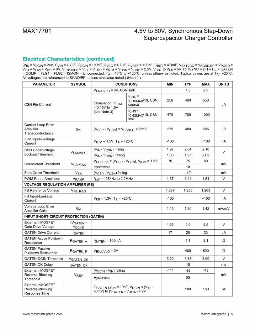
PARAMETER SYMBOL CONDITIONS MIN TYP MAX UNITSSYNC High Pulse-Width 100 nsSYNC Low Pulse-Width 100 nsSYNC Input-LeakageCurrent ISYNC_LKG VRT/SYNC = 2.5V, TA= +25ºC -100 +100 nA
REFERENCE VOLTAGE (VREF)VREF Output Voltage VREF IVREF = 0 to 1mA 2.465 2.500 2.535 VReference Current Limit IREF_LIM VREF = 2.45V 1.2 1.8 2.7 mACURRENT SENSE (CSP, CSN, ILIM)CSP, CSN CommonMode Voltage Range 0 (VIN - 2) V
CSP to CSN InputOperating Voltage VDIFF_CS VDIFF_CS = (VCSP - VCSN) -10 +100 mV
FLG1/FLG2 LeakageCurrent VFLG1, VFLG2 = 5.5V, TA = +25ºC -100 +100 nA
IC THERMAL PROTECTION
Thermal ShutdownThreshold
Temperature rising 160°C
Hysteresis 10
Note 2: Electrical specifications are production tested at TA = +25ºC. Specifications over the entire operating temperature range areguaranteed by design and characterization.
MAX17701 4.5V to 60V, Synchronous Step-DownSupercapacitor Charger Controller
www.maximintegrated.com Maxim Integrated | 6
Note 3: CC mode charging current setting is calculated using this equation:
ICHGMAX =VCSREG
RSwhere RS is the current sense resistor.
MAX17701 4.5V to 60V, Synchronous Step-DownSupercapacitor Charger Controller
www.maximintegrated.com Maxim Integrated | 7
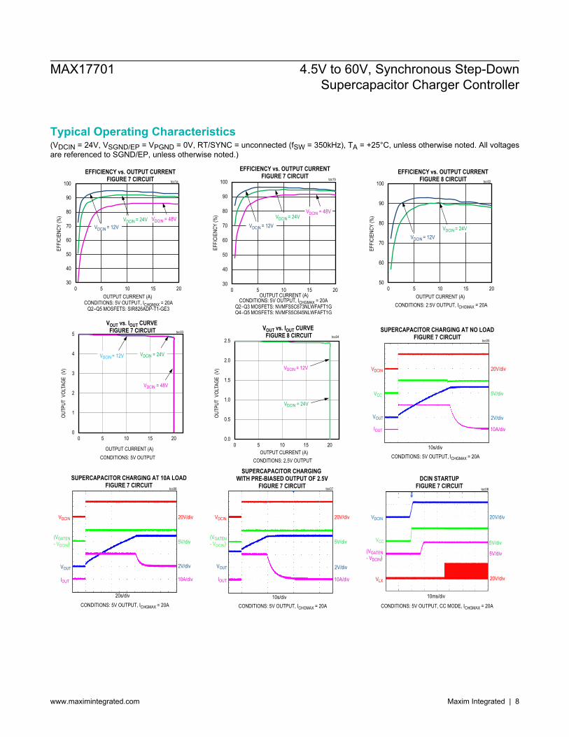
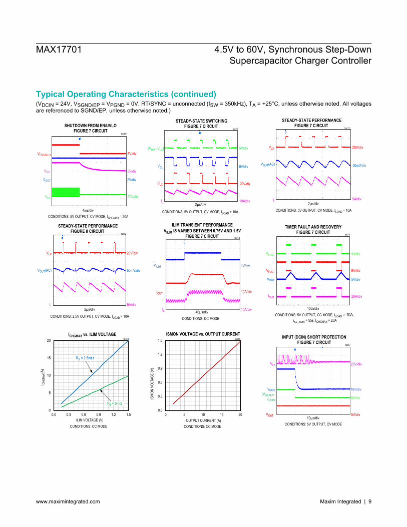
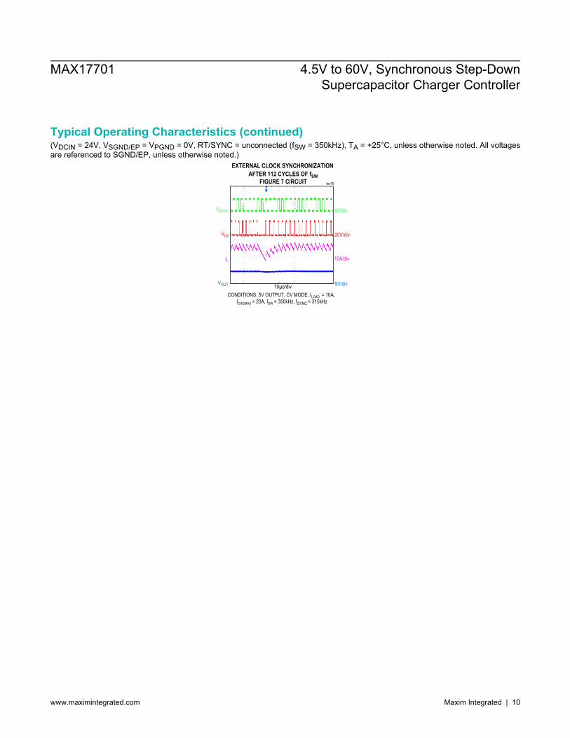
Typical Operating Characteristics(VDCIN = 24V, VSGND/EP = VPGND = 0V, RT/SYNC = unconnected (fSW = 350kHz), TA = +25°C, unless otherwise noted. All voltagesare referenced to SGND/EP, unless otherwise noted.)
MAX17701 4.5V to 60V, Synchronous Step-DownSupercapacitor Charger Controller
MAX17701 4.5V to 60V, Synchronous Step-DownSupercapacitor Charger Controller
www.maximintegrated.com Maxim Integrated | 10
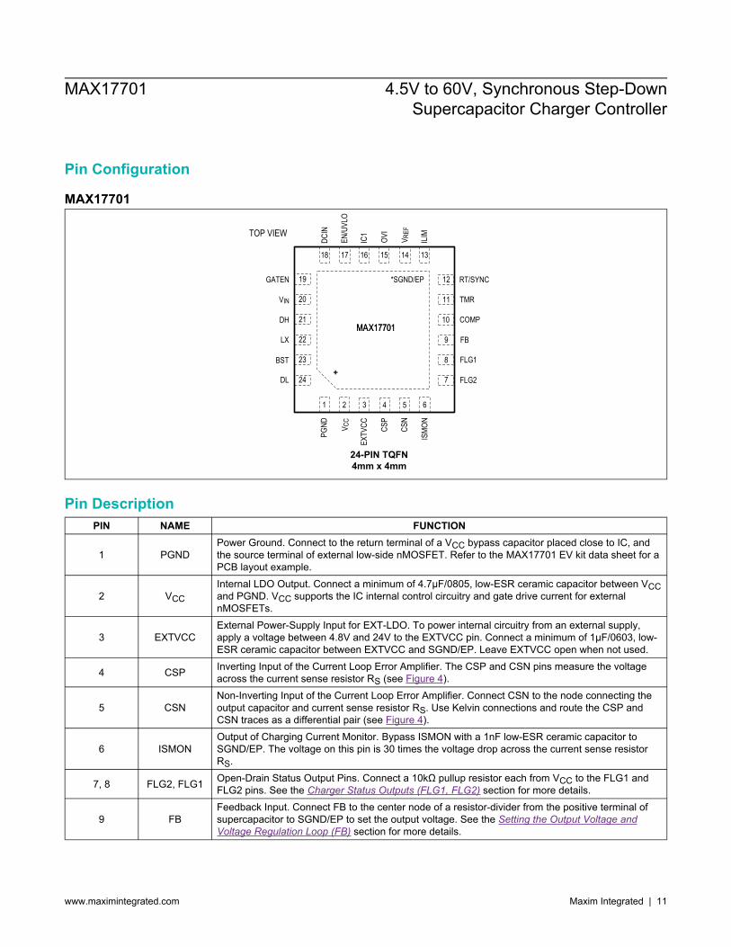
Pin Configuration
MAX17701
V CC
CSP
CSN
ISMO
N
PGND
EN/U
VLO
OVI
V REF
DCIN
ILIM
LX
BST
DL
COMP
FB
FLG2
EXTV
CCIC
1
DH
TMRVIN
RT/SYNCGATEN
24-PIN TQFN4mm x 4mm
TOP VIEW
+
12
11
10
9
8
7
MMAAXX1177770011
*SGND/EP
131415161718
19
20
21
22
23
24
1 2 3 4 5 6
FLG1
Pin DescriptionPIN NAME FUNCTION
1 PGNDPower Ground. Connect to the return terminal of a VCC bypass capacitor placed close to IC, andthe source terminal of external low-side nMOSFET. Refer to the MAX17701 EV kit data sheet for aPCB layout example.
2 VCCInternal LDO Output. Connect a minimum of 4.7μF/0805, low-ESR ceramic capacitor between VCCand PGND. VCC supports the IC internal control circuitry and gate drive current for externalnMOSFETs.
3 EXTVCCExternal Power-Supply Input for EXT-LDO. To power internal circuitry from an external supply,apply a voltage between 4.8V and 24V to the EXTVCC pin. Connect a minimum of 1μF/0603, low-ESR ceramic capacitor between EXTVCC and SGND/EP. Leave EXTVCC open when not used.
4 CSP Inverting Input of the Current Loop Error Amplifier. The CSP and CSN pins measure the voltageacross the current sense resistor RS (see Figure 4).
5 CSNNon-Inverting Input of the Current Loop Error Amplifier. Connect CSN to the node connecting theoutput capacitor and current sense resistor RS. Use Kelvin connections and route the CSP andCSN traces as a differential pair (see Figure 4).
6 ISMONOutput of Charging Current Monitor. Bypass ISMON with a 1nF low-ESR ceramic capacitor toSGND/EP. The voltage on this pin is 30 times the voltage drop across the current sense resistorRS.
7, 8 FLG2, FLG1 Open-Drain Status Output Pins. Connect a 10kΩ pullup resistor each from VCC to the FLG1 andFLG2 pins. See the Charger Status Outputs (FLG1, FLG2) section for more details.
9 FBFeedback Input. Connect FB to the center node of a resistor-divider from the positive terminal ofsupercapacitor to SGND/EP to set the output voltage. See the Setting the Output Voltage andVoltage Regulation Loop (FB) section for more details.
MAX17701 4.5V to 60V, Synchronous Step-DownSupercapacitor Charger Controller
www.maximintegrated.com Maxim Integrated | 11
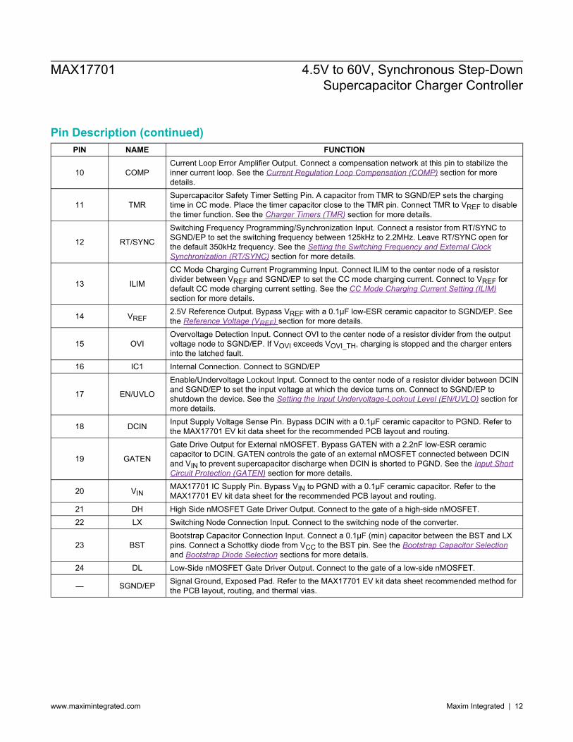
Pin Description (continued)PIN NAME FUNCTION
10 COMPCurrent Loop Error Amplifier Output. Connect a compensation network at this pin to stabilize theinner current loop. See the Current Regulation Loop Compensation (COMP) section for moredetails.
11 TMRSupercapacitor Safety Timer Setting Pin. A capacitor from TMR to SGND/EP sets the chargingtime in CC mode. Place the timer capacitor close to the TMR pin. Connect TMR to VREF to disablethe timer function. See the Charger Timers (TMR) section for more details.
12 RT/SYNC
Switching Frequency Programming/Synchronization Input. Connect a resistor from RT/SYNC toSGND/EP to set the switching frequency between 125kHz to 2.2MHz. Leave RT/SYNC open forthe default 350kHz frequency. See the Setting the Switching Frequency and External ClockSynchronization (RT/SYNC) section for more details.
13 ILIM
CC Mode Charging Current Programming Input. Connect ILIM to the center node of a resistordivider between VREF and SGND/EP to set the CC mode charging current. Connect to VREF fordefault CC mode charging current setting. See the CC Mode Charging Current Setting (ILIM)section for more details.
14 VREF2.5V Reference Output. Bypass VREF with a 0.1μF low-ESR ceramic capacitor to SGND/EP. Seethe Reference Voltage (VREF) section for more details.
15 OVIOvervoltage Detection Input. Connect OVI to the center node of a resistor divider from the outputvoltage node to SGND/EP. If VOVI exceeds VOVI_TH, charging is stopped and the charger entersinto the latched fault.
16 IC1 Internal Connection. Connect to SGND/EP
17 EN/UVLO
Enable/Undervoltage Lockout Input. Connect to the center node of a resistor divider between DCINand SGND/EP to set the input voltage at which the device turns on. Connect to SGND/EP toshutdown the device. See the Setting the Input Undervoltage-Lockout Level (EN/UVLO) section formore details.
18 DCIN Input Supply Voltage Sense Pin. Bypass DCIN with a 0.1μF ceramic capacitor to PGND. Refer tothe MAX17701 EV kit data sheet for the recommended PCB layout and routing.
19 GATEN
Gate Drive Output for External nMOSFET. Bypass GATEN with a 2.2nF low-ESR ceramiccapacitor to DCIN. GATEN controls the gate of an external nMOSFET connected between DCINand VIN to prevent supercapacitor discharge when DCIN is shorted to PGND. See the Input ShortCircuit Protection (GATEN) section for more details.
20 VINMAX17701 IC Supply Pin. Bypass VIN to PGND with a 0.1μF ceramic capacitor. Refer to theMAX17701 EV kit data sheet for the recommended PCB layout and routing.
21 DH High Side nMOSFET Gate Driver Output. Connect to the gate of a high-side nMOSFET.22 LX Switching Node Connection Input. Connect to the switching node of the converter.
23 BSTBootstrap Capacitor Connection Input. Connect a 0.1μF (min) capacitor between the BST and LXpins. Connect a Schottky diode from VCC to the BST pin. See the Bootstrap Capacitor Selectionand Bootstrap Diode Selection sections for more details.
24 DL Low-Side nMOSFET Gate Driver Output. Connect to the gate of a low-side nMOSFET.
— SGND/EP Signal Ground, Exposed Pad. Refer to the MAX17701 EV kit data sheet recommended method forthe PCB layout, routing, and thermal vias.
MAX17701 4.5V to 60V, Synchronous Step-DownSupercapacitor Charger Controller
www.maximintegrated.com Maxim Integrated | 12
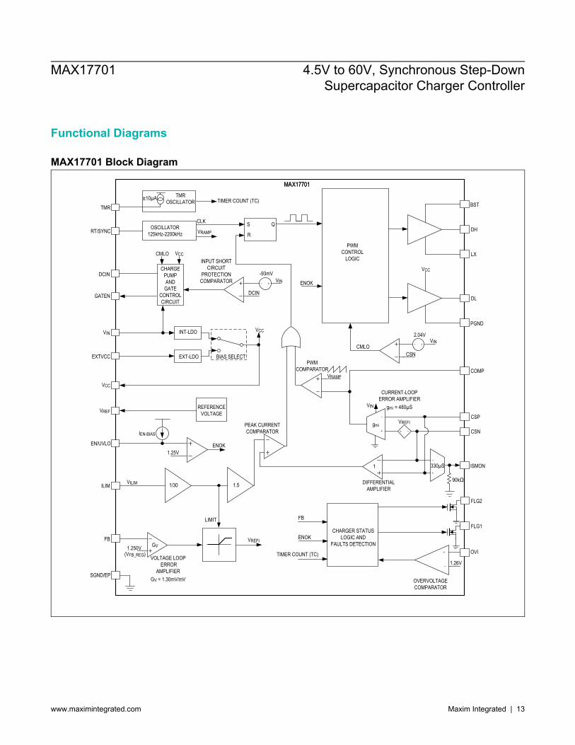
Functional Diagrams
MAX17701 Block Diagram
SGND/EP
OSCILLATOR125kHz-2200kHzRT/SYNC DH
DL
S
R
Q
PGND
LX
BST
CLK
VCC
VIN
DCIN
GATEN
CHARGE PUMP AND
GATE CONTROL CIRCUIT
EN/UVLO1.25V
IEN-BIAS
OVI
CHARGER STATUS LOGIC AND
FAULTS DETECTION
OVERVOLTAGECOMPARATOR
ILIM
VREF
VCC
ENOK
FB
CSN
CSP
COMPVRAMP
PWMCOMPARATOR
INPUT SHORT CIRCUIT
PROTECTIONCOMPARATOR
DCIN
PWMCONTROL
LOGIC
VRAMP
PEAK CURRENTCOMPARATOR
VIN-93mV
CSN
VIN
EXTVCC
330µS ISMON
CMLO
MMAAXX1177770011
CURRENT-LOOP ERROR AMPLIFIER
gmi = 480µS
CMLO
VCC
90kΩ
2.04V
BIAS SELECT
INT-LDO
EXT-LDO
VCC
gmi
1.26V
VIN
VILIM
ENOK
VREFI
REFERENCE VOLTAGE
1/30 DIFFERENTIAL AMPLIFIER
GV
(VFB_REG)1.250V
VOLTAGE LOOPERROR
AMPLIFIERGV = 1.30mV/mV
LIMIT
VREFI
1.5
1
±10µA TMROSCILLATOR
TMRTIMER COUNT (TC)
TIMER COUNT (TC)
FB
ENOK
FLG1
FLG2
MAX17701 4.5V to 60V, Synchronous Step-DownSupercapacitor Charger Controller
www.maximintegrated.com Maxim Integrated | 13
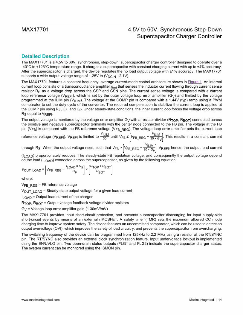
Detailed DescriptionThe MAX17701 is a 4.5V to 60V, synchronous, step-down, supercapacitor charger controller designed to operate over a-40°C to +125°C temperature range. It charges a supercapacitor with constant charging current with up to ±4% accuracy.After the supercapacitor is charged, the device regulates the no load output voltage with ±1% accuracy. The MAX17701supports a wide output-voltage range of 1.25V to (VDCIN - 2.1V).The MAX17701 features a constant frequency, average current-mode control architecture shown in Figure 1. An internalcurrent loop consists of a transconductance amplifier gmi that senses the inductor current flowing through current senseresistor RS as a voltage drop across the CSP and CSN pins. The current sense voltage is compared with a currentloop reference voltage (VREFI), which is set by the outer voltage loop error amplifier (GV) and limited by the voltageprogrammed at the ILIM pin (VILIM). The voltage at the COMP pin is compared with a 1.44V (typ) ramp using a PWMcomparator to set the duty cycle of the converter. The required compensation to stabilize the current loop is applied atthe COMP pin using RZ, CZ, and CP. Under steady-state conditions, the inner current loop forces the voltage drop acrossRS equal to VREFI.The output voltage is monitored by the voltage error amplifier GV with a resistor divider (RTOP, RBOT) connected acrossthe positive and negative supercapacitor terminals with the center node connected to the FB pin. The voltage at the FBpin (VFB) is compared with the FB reference voltage (VFB_REG). The voltage loop error amplifier sets the current loop
reference voltage (VREFI). VREFI is limited toVILIM
30 until VFB ≤ [VFB_REG −VILIM
30 × GV ]. This results in a constant current
through RS. When the output voltage rises, such that VFB > [VFB_REG −VILIM
30 × GV ], VREFI; hence, the output load current
(ILOAD) proportionately reduces. The steady-state FB regulation voltage, and consequently the output voltage dependon the load (ILOAD) connected across the supercapacitor, as given by the following equation:
VOUT_LOAD = [VFB_REG −ILOAD × RS
GV ] × [RTOP + RBOTRBOT ]
where,VFB_REG = FB reference voltageVOUT_LOAD = Steady-state output voltage for a given load currentILOAD = Output load current of the chargerRTOP, RBOT = Output voltage feedback voltage divider resistorsGV = Voltage loop error amplifier gain (1.30mV/mV)The MAX17701 provides input short-circuit protection, and prevents supercapacitor discharging for input supply-sideshort-circuit events by means of an external nMOSFET. A safety timer (TMR) sets the maximum allowed CC modecharging time to improve system safety. The device features an uncommitted comparator, which can be used to detect anoutput overvoltage (OVI), which improves the safety of load circuitry, and prevents the supercapacitor from overcharging.The switching frequency of the device can be programmed from 125kHz to 2.2 MHz using a resistor at the RT/SYNCpin. The RT/SYNC also provides an external clock synchronization feature. Input undervoltage lockout is implementedusing the EN/UVLO pin. Two open-drain status outputs (FLG1 and FLG2) indicate the supercapacitor charger status.The system current can be monitored using the ISMON pin.
MAX17701 4.5V to 60V, Synchronous Step-DownSupercapacitor Charger Controller
www.maximintegrated.com Maxim Integrated | 14
FB
CSN
CSP
COMP
PWMCOMPARATOR
CURRENT-LOOPERROR AMPLIFIER
gmi = 480µS
VOLTAGE LOOPERROR AMPLIFIER
GV = 1.30mV/mV
RZCP
CZ
RS
RTOP
RBOTCFB
L
COUTSUPERCAPACITOR
VIN
LX
SYSTEM LOAD
1.250V (TYP)(VFB_REG)
gmi
VILIM
MMAAXX1177770011
R1
C1
DH
DL
ILIM
VRAMP
VREFI
VOUT
GV
VREFI
1/30
LIMIT
SW
1f
tS =
Figure 1. Average Current Mode Control Loop
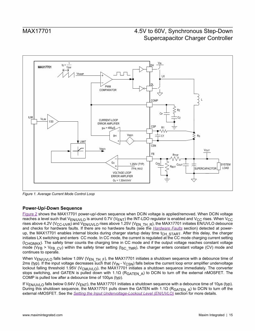
Power-Up/-Down SequenceFigure 2 shows the MAX17701 power-up/-down sequence when DCIN voltage is applied/removed. When DCIN voltagereaches a level such that VEN/UVLO is around 0.7V (VENT) the INT-LDO regulator is enabled and VCC rises. When VCCrises above 4.2V (VCC-UVR) and VEN/UVLO rises above 1.25V (VEN_TH_R), the MAX17701 initiates EN/UVLO debounceand checks for hardware faults. If there are no hardware faults (see the Hardware Faults section) detected at power-up, the MAX17701 enables internal blocks during charger startup delay time tCH_START. After this delay, the chargerinitiates LX switching and enters CC mode. In CC mode, the current is regulated at the CC mode charging current setting(ICHGMAX). The safety timer counts the charging time in CC mode and if the output voltage reaches constant voltagemode (VFB > VFB_CV) within the safety timer setting (tSC_TMR), the charger enters constant voltage (CV) mode andcontinues to operate.When VEN/UVLO falls below 1.09V (VEN_TH_F), the MAX17701 initiates a shutdown sequence with a debounce time of2ms (typ). If the input voltage decreases such that (VIN - VCSN) falls below the current loop error amplifier undervoltagelockout falling threshold 1.95V (VCMUVLO), the MAX17701 initiates a shutdown sequence immediately. The converterstops switching, and GATEN is pulled down with 1.1Ω (RGATEN_A) to DCIN to turn off the external nMOSFET. TheCOMP is pulled low after a debounce time of 100μs (typ).If VEN/UVLO falls below 0.64V (VENT), the MAX17701 initiates a shutdown sequence with a debounce time of 10μs (typ).During this shutdown sequence, the MAX17701 pulls down the GATEN with 1.1Ω (RGATEN_A) to DCIN to turn off theexternal nMOSFET. See the Setting the Input Undervoltage-Lockout Level (EN/UVLO) section for more details.
MAX17701 4.5V to 60V, Synchronous Step-DownSupercapacitor Charger Controller
www.maximintegrated.com Maxim Integrated | 15
VDCIN
VCC
VTMR
VOUT, VFB
IOUT or ICHG CC MODE
1.5V
0.96V
CHARGER ON AND TIMER COUNT START
VEN/UVLO
CV MODE
tSC_TMR
TIMER COUNT STOPS AND RESETS
tCH_START (27ms)
VOUT
VFB
(VGATEN - VDCIN)5V
GATEN ENABLE
VFB = VFB_CV
EN/UVLO DEBOUNCETIME (2ms)
POWER-UP START
POWER-DOWN START
tTC < tSC_TMR
ICHGMAX
CHARGER OFF CHARGER ON CHARGER OFF
VENT (0.64V FALLING)
6ms
24ms
VEN_TH_R (1.25V)VEN_TH_F (1.09V)
VCC_UVR (4.2V)
VENT (0.7V RISING)
t
t
t
t
t
t
VFB_CV (1.219V)
t
80%
NOTE: NOT TO SCALE
FLG1
FLG2HIGH-Z LOW
HIGH-Z LOWHIGH-Z
LOW
t
t
HIGH-Z
HIGH-Z
Figure 2. Charger Power-Up/-Down Sequence
MAX17701 4.5V to 60V, Synchronous Step-DownSupercapacitor Charger Controller
www.maximintegrated.com Maxim Integrated | 16
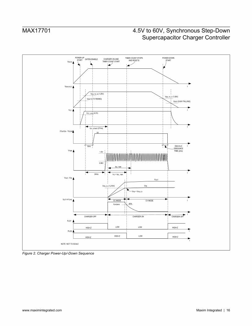
Input Short-Circuit Protection (GATEN)The MAX17701 provides gate drive output (GATEN) that drives a logic-level gate threshold external nMOSFET, whichturns off and prevents supercapacitor discharging for input supply short-circuit events. The GATEN is pulled up with20μA (IGATEN) when VIN is 2.04V (VCMUVLO) above VCSN. If VGATEN does not reach 3.55V (VGATEN_OK) within 15ms(tGATEN_OK), MAX17701 enters latched hardware fault.Figure 3 depicts the MAX17701 behavior when DCIN is shorted to PGND. When VDCIN is 93mV (VREV) below VIN,GATEN is pulled down with 1.1Ω (RGATEN_A) and the external nMOSFET is turned off within 100ns (typ). When VEN/UVLO goes below 0.64V (VENT), the MAX17701 shuts down with 10μs (typ) debounce time. When DCIN-to-PGND shortis removed, the power-up sequence is initiated (see the Power-Up/Down Sequence section). When the input short-circuitprotection is not used, connect a 2.2nF capacitor between GATEN and DCIN, and short DCIN to VIN.
VD OF EXTERNAL nMOSFET
VDCIN
VEN/UVLO
VREV (-93mV)
(VDCIN - VIN)
(VGATEN - VDCIN)
VLX
VCC
VCC_UVR (4.2V)
EXTERNAL nMOSFET TURNS OFF CHARGING STARTSVGATEN_OK CHECKDCIN SHORTED TO PGND
DCIN SHORT TO PGND FAULT RECOVERY
5V
NOTE: NOT TO SCALE
0mV
VGATEN_OK (3.55V)
CHARGING STOPS
tGATEN_OK (15ms)
6ms
VEN_TH_R (1.25V)
VENT (0.7V)
10µs
tREV (100ns)
tCH_START
(27ms)
t
t
t
t
t
t
5V
2V
Figure 3. Input Short-Circuit Protection and Recovery Timing Diagram
MAX17701 4.5V to 60V, Synchronous Step-DownSupercapacitor Charger Controller
www.maximintegrated.com Maxim Integrated | 17
Charger OperationMAX17701 offers constant current (CC) mode and constant voltage (CV) mode for charging a supercapacitor. In CCmode, the charging current is regulated to the CC mode charging current (ICHGMAX) proportional to VILIM. The safetytimer starts counting when the device enters CC mode. When VFB goes above 1.219V (VFB_CV) within the CC modetimeout period (tSC_TMR), the charger enters CV mode and the safety timer stops counting (see Charger Timers (TMR)section). The safety timer count resets when the device enters CV mode. In CV mode, the device continues to chargethe supercapacitor until VFB reaches 1.250V (VFB_REG). The charger regulates VFB at VFB_REG at no load. When VFBdrops below 1.215V (VFB_CV), the charger exits CV mode, enters CC mode, and the timer count restarts.
Charger Timers (TMR)The MAX17701 offers a programmable timer feature to provide additional safety to the supercapacitor and the connectedload. Connect a capacitor from TMR to SGND/EP to enable the timer feature. Connect TMR to VREF to disable the timerfeature. The timer counts the charging time in CC mode. If VFB does not reach 1.219V (VFB_CV) within CC mode timeoutperiod (tSC_TMR), the charger turns off. The charger restarts after 4 times tSC_TMR. The MAX17701 supports 470pF to10μF capacitance on TMR, translating into a CC mode timeout period range of 1.5 second to 9 hours.The safety timer is programmed based on maximum supercapacitor value (CSUP), output voltage (VOUT), and CC modecharging current setting (ICHGMAX). Refer to the CC Mode Charging Current Setting (ILIM) section.Choose the required safety timer period using the following equation:
tSC_TMR ≥CSUP × VOUT
ICHGMAX − ILOAD
where ILOAD is the system load during the supercapacitor charging periodSelect ICHGMAX ≥ 1.5 × ILOAD to ensure the charger enters CV mode
Use the following equation to calculate CTMR for the required tSC_TMR:
CTMR ≥ 1.15 ×( tSC_TMR2 × tFCHG
- 1.2 × 10 − 6) × ( ITMRVTMR_H − VTMR_L )
wheretSC_TMR = Desired safety timer timeout setting in secondsCTMR = TMR capacitor in FaradtFCHG = Number of TMR cycles in CC mode (32767)VTMR_H = TMR oscillator upper threshold (1.5V)VTMR_L = TMR oscillator lower threshold (0.96V)ITMR = TMR pin source/sink current (10μA)
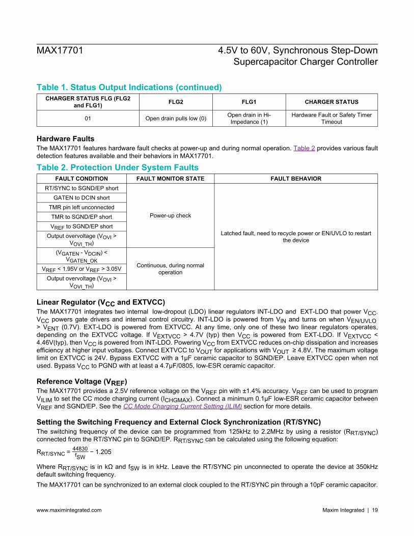
Charger Status Outputs (FLG1, FLG2)The MAX17701 features two open-drain status output pins (FLG1 and FLG2) to indicate the status of the charger. Table1 shows the status flag summary.
Table 1. Status Output IndicationsCHARGER STATUS FLG (FLG2
and FLG1) FLG2 FLG1 CHARGER STATUS
11 Open drain in Hi-Impedance (1)
Open drain in Hi-Impedance (1) Charger Off
10 Open drain in Hi-Impedance (1) Open drain pulls low (0) CC Mode
00 Open drain pulls low (0) Open drain pulls low (0) CV Mode
MAX17701 4.5V to 60V, Synchronous Step-DownSupercapacitor Charger Controller
www.maximintegrated.com Maxim Integrated | 18
Table 1. Status Output Indications (continued)CHARGER STATUS FLG (FLG2
and FLG1) FLG2 FLG1 CHARGER STATUS
01 Open drain pulls low (0) Open drain in Hi-Impedance (1)
Hardware Fault or Safety TimerTimeout
Hardware FaultsThe MAX17701 features hardware fault checks at power-up and during normal operation. Table 2 provides various faultdetection features available and their behaviors in MAX17701.
Table 2. Protection Under System FaultsFAULT CONDITION FAULT MONITOR STATE FAULT BEHAVIOR
RT/SYNC to SGND/EP short
Power-up check
Latched fault, need to recycle power or EN/UVLO to restartthe device
GATEN to DCIN shortTMR pin left unconnectedTMR to SGND/EP shortVREF to SGND/EP short
Output overvoltage (VOVI >VOVI_TH)
(VGATEN - VDCIN) <VGATEN_OK
Continuous, during normaloperationVREF < 1.95V or VREF > 3.05V
Output overvoltage (VOVI >VOVI_TH)
Linear Regulator (VCC and EXTVCC)The MAX17701 integrates two internal low-dropout (LDO) linear regulators INT-LDO and EXT-LDO that power VCC.VCC powers gate drivers and internal control circuitry. INT-LDO is powered from VIN and turns on when VEN/UVLO> VENT (0.7V). EXT-LDO is powered from EXTVCC. At any time, only one of these two linear regulators operates,depending on the EXTVCC voltage. If VEXTVCC > 4.7V (typ) then VCC is powered from EXT-LDO. If VEXTVCC <4.46V(typ), then VCC is powered from INT-LDO. Powering VCC from EXTVCC reduces on-chip dissipation and increasesefficiency at higher input voltages. Connect EXTVCC to VOUT for applications with VOUT ≥ 4.8V. The maximum voltagelimit on EXTVCC is 24V. Bypass EXTVCC with a 1μF ceramic capacitor to SGND/EP. Leave EXTVCC open when notused. Bypass VCC to PGND with at least a 4.7µF/0805, low-ESR ceramic capacitor.
Reference Voltage (VREF)The MAX17701 provides a 2.5V reference voltage on the VREF pin with ±1.4% accuracy. VREF can be used to programVILIM to set the CC mode charging current (ICHGMAX). Connect a minimum 0.1μF low-ESR ceramic capacitor betweenVREF and SGND/EP. See the CC Mode Charging Current Setting (ILIM) section for more details.
Setting the Switching Frequency and External Clock Synchronization (RT/SYNC)The switching frequency of the device can be programmed from 125kHz to 2.2MHz by using a resistor (RRT/SYNC)connected from the RT/SYNC pin to SGND/EP. RRT/SYNC can be calculated using the following equation:
RRT/SYNC = 44830fSW
− 1.205
Where RRT/SYNC is in kΩ and fSW is in kHz. Leave the RT/SYNC pin unconnected to operate the device at 350kHzdefault switching frequency.The MAX17701 can be synchronized to an external clock coupled to the RT/SYNC pin through a 10pF ceramic capacitor.
MAX17701 4.5V to 60V, Synchronous Step-DownSupercapacitor Charger Controller
www.maximintegrated.com Maxim Integrated | 19
The external clock is detected after checking the rising edge for 112 cycles of the internal clock (set by RT/SYNC). Ifthe external clock frequency is within the allowed SYNC frequency range (±10% of nominal internal clock frequency), thedevice stops switching for 2 switching time periods and then restarts with an external clock. When the external clock isremoved, the device stops switching for 10 switching time periods and then restarts with an internal clock.The minimum external clock pulse-width should be greater than 100ns. The off-time duration of the external clock shouldbe at least 100ns.
Peak Current-LimitThe MAX17701 provides a cycle-by-cycle overcurrent protection by limiting the peak current-sense voltage (VCSP- VCSN) across the current sense pins. When an overcurrent event ((VCSP - VCSN) > VCSPEAK) is detected, theovercurrent comparator in the MAX17701 terminates the DH pulse and limits the peak current. The overcurrent fault isnot latched.
Charging Current Monitoring (ISMON)The output charge current can be monitored by observing the voltage at the ISMON pin. Connect a 1nF ceramic capacitoron ISMON to filter out the switching frequency component in the ISMON voltage. The charging current is given by thefollowing equation:
ICHG =VISMON30 × RS
where,ICHG = Charging currentVISMON = Voltage at the ISMON pinRS = Current-sense resistance
Thermal-Shutdown ProtectionThermal-shutdown protection limits junction temperature of the device. When the junction temperature of the deviceexceeds +160ºC, an on-chip thermal sensor shuts down the device, allowing the device to cool. The device turns on afterthe junction temperature reduces by 10ºC. Carefully evaluate the total power dissipation to avoid unwanted triggering ofthe thermal shutdown during normal operation (see the Device Power Dissipation section).
MAX17701 4.5V to 60V, Synchronous Step-DownSupercapacitor Charger Controller
www.maximintegrated.com Maxim Integrated | 20
Applications Information
Inductor SelectionThree key inductor parameters must be specified for operation with the device: inductance value (L), DC resistance(RDCR), and inductor saturation current (ISAT).The required inductance is calculated based on the inductor current ripple ratio (LIR), i.e., ratio of peak-to-peak ripplecurrent (ΔIL) to CC mode charging current (ICHGMAX). A good compromise between size and loss is an LIR of 0.3.The inductance value (L) is given by the higher value of the two calculated inductances:
L1 =VOUT x (1-D)
LIR × ICHGMAX x fSW
L2 =VOUT
600000 × ICHGMAX
where:VOUT = Desired voltage across supercapacitorICHGMAX = CC mode charging currentD = Duty cycle of the converter, VOUT/VINVIN = Nominal input voltagefSW = Switching frequencySelect an inductor that is nearest to the calculated value. The inductor RMS-current rating should be more than the CCmode charging current. Select a low-loss inductor with acceptable dimensions and the lowest possible DC resistance.The saturation current rating (ISAT) of the inductor must be high enough to ensure that saturation can occur only abovethe overcurrent threshold corresponding to VCSPEAK.
Output Capacitor SelectionSupercapacitors have significant equivalent series resistance (ESRSUP). The switching ripple component of chargeroutput current flows into this ESRSUP and results in a large output-voltage ripple. To reduce the voltage ripple across thesupercapacitor, additional X7R ceramic capacitors and/or low-ESR POSCAP capacitors can be used at the output of thecharger.X7R ceramic output capacitors are preferred due to their stability over temperature in industrial applications. For highervalues of output capacitance, low-ESR POSCAP capacitors can be used in parallel with ceramic capacitors.Calculate the required output capacitance (COUT) based on the following equation:
COUT =25 × ICHGMAX
fSW× VOUT
where:ICHGMAX = CC mode charging current settingfSW = Switching frequencyVOUT = Desired voltage across the supercapacitorDerating of ceramic capacitors with DC-bias voltage must be considered while selecting the capacitors, using themanufacturer data sheet. The selected output capacitor COUT_SEL and its equivalent series resistance (ESRCOUT) affectthe output-voltage ripple (ΔVOUT). Estimate the resultant ΔVOUT using the following equation:
ΔVOUT ≈ ΔIL × (ESRCOUT + 18 × fSW × COUT_SEL )
MAX17701 4.5V to 60V, Synchronous Step-DownSupercapacitor Charger Controller
www.maximintegrated.com Maxim Integrated | 21
where ΔIL is the inductor peak-to-peak ripple current.
Input Capacitor SelectionThe input filter capacitor reduces peak currents drawn from the power source and reduces noise and voltage ripple onthe input caused by the switching converter. Calculate the required input capacitance at VIN (CVIN) using the followingequation:
CVIN =ICHGMAX × D × (1 − D)
η × fSW × ∆VIN
where:
D =VOUT
VINis the duty ratio of the converter
fSW = Switching frequencyΔVIN = Allowable input-voltage rippleη = Efficiency of the converterICHGMAX = CC mode charging currentChoose ΔVIN ≤ 0.5V to minimize voltage ripple across the external nMOSFET and to provide robust operation duringinput short-circuit events.The input capacitor RMS current (IRMS) is calculated using the following equation:
IRMS = ICHGMAX × √VOUT × [VIN − VOUT]VIN
Choose low-ESR ceramic input capacitors that exhibit less than a +10°C temperature rise at IRMS for optimal long-termreliability. X7R capacitors are recommended in industrial applications for their temperature stability. Derating of ceramiccapacitors with DC-bias voltage must be considered while selecting the capacitors using the manufacturer data sheet.Choose an electrolytic capacitor at DCIN in order to prevent the DCIN voltage from being less than -0.3V during inputshort events. An electrolytic capacitor also provides the damping for potential oscillations caused by inductance of thelonger input power path and input ceramic capacitor (CVIN). Additionally, if required, add a Schottky diode at DCIN inparallel with the electrolytic capacitor.
Operating Input-Voltage RangeThe following equations are used to calculate the operating input-voltage range for a given output voltage and CC modecharging current setting. The minimum operating input voltage on the DCIN pin is given by the higher value from the twocalculated voltages:
where:VDCIN(MIN1), VDCIN(MIN2) = Minimum operating input voltages; the higher of the two values is the minimum operatinginput voltage (VDCIN(MIN))VOUT = Desired regulation voltage across the supercapacitorICHGMAX = CC mode charging current settingfSW = Switching frequency in Hz
MAX17701 4.5V to 60V, Synchronous Step-DownSupercapacitor Charger Controller
www.maximintegrated.com Maxim Integrated | 22
RDCR(MAX) = Worst-case DC resistance of the inductor in ΩRDS_ON(HS), RDS_ON(LS) = Worst-case on-state resistances of high-side and low-side internal MOSFETs in Ω,respectivelytDT_HL = Dead time (30ns)tMIN_ON_DL(MAX) = Worst-case DL minimum controlled on-time (100ns).The maximum operating input voltage on the DCIN pin is calculated as follows:
VDCIN(MAX) =VOUT
(1.05 × fSW × tMIN_ON_DH(MAX))where tMIN_ON_DH(MAX) is the worst-case DH minimum controlled on-time (100ns).
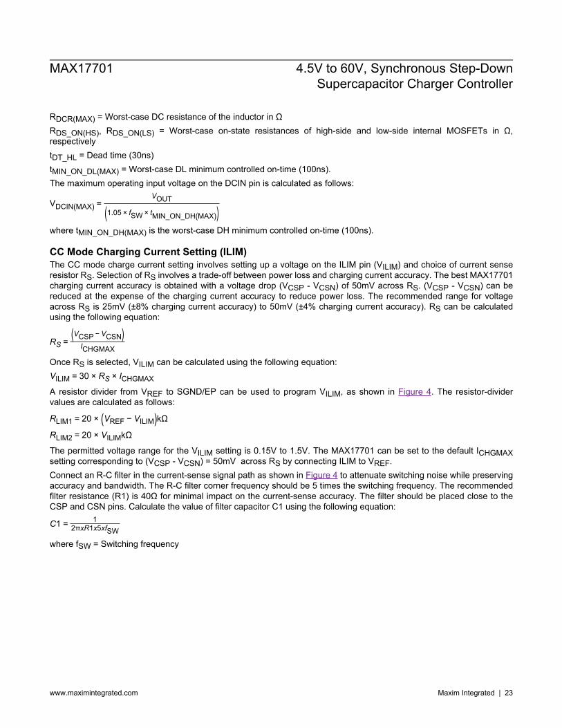
CC Mode Charging Current Setting (ILIM)The CC mode charge current setting involves setting up a voltage on the ILIM pin (VILIM) and choice of current senseresistor RS. Selection of RS involves a trade-off between power loss and charging current accuracy. The best MAX17701charging current accuracy is obtained with a voltage drop (VCSP - VCSN) of 50mV across RS. (VCSP - VCSN) can bereduced at the expense of the charging current accuracy to reduce power loss. The recommended range for voltageacross RS is 25mV (±8% charging current accuracy) to 50mV (±4% charging current accuracy). RS can be calculatedusing the following equation:
RS =(VCSP − VCSN)
ICHGMAX
Once RS is selected, VILIM can be calculated using the following equation:VILIM = 30 × RS × ICHGMAX
A resistor divider from VREF to SGND/EP can be used to program VILIM, as shown in Figure 4. The resistor-dividervalues are calculated as follows:
RLIM1 = 20 × (VREF − VILIM)kΩ
RLIM2 = 20 × VILIMkΩ
The permitted voltage range for the VILIM setting is 0.15V to 1.5V. The MAX17701 can be set to the default ICHGMAXsetting corresponding to (VCSP - VCSN) = 50mV across RS by connecting ILIM to VREF.Connect an R-C filter in the current-sense signal path as shown in Figure 4 to attenuate switching noise while preservingaccuracy and bandwidth. The R-C filter corner frequency should be 5 times the switching frequency. The recommendedfilter resistance (R1) is 40Ω for minimal impact on the current-sense accuracy. The filter should be placed close to theCSP and CSN pins. Calculate the value of filter capacitor C1 using the following equation:
C1 = 12πxR1x5xfSW
where fSW = Switching frequency
MAX17701 4.5V to 60V, Synchronous Step-DownSupercapacitor Charger Controller
www.maximintegrated.com Maxim Integrated | 23
DH
DL
LX
C1
CSP
CSN
R1
L
COUT SUPERCAPACITOR
RS
PGND
SYSTEM LOAD
VIN
MMAAXX1177770011
TO CSNCURRENT-SENSE RESISTOR LAYOUT
VREF
ILIM
SGND/EP
RLIM1
RLIM2
ICHG
ICHG
RS
To CSP
Figure 4. Current-Sense Circuit
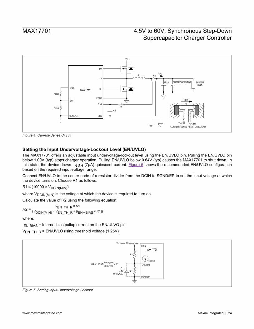
Setting the Input Undervoltage-Lockout Level (EN/UVLO)The MAX17701 offers an adjustable input undervoltage-lockout level using the EN/UVLO pin. Pulling the EN/UVLO pinbelow 1.09V (typ) stops charger operation. Pulling EN/UVLO below 0.64V (typ) causes the MAX17701 to shut down. Inthis state, the device draws IIN-SH (7μA) quiescent current. Figure 5 shows the recommended EN/UVLO configurationbased on the required input-voltage range.Connect EN/UVLO to the center node of a resistor divider from the DCIN to SGND/EP to set the input voltage at whichthe device turns on. Choose R1 as follows:R1 ≤ (10000 × VDCIN(MIN))
where VDCIN(MIN) is the voltage at which the device is required to turn on.Calculate the value of R2 using the following equation:
R2 =VEN_TH_R × R1
(VDCIN(MIN) − VEN_TH_R + (IEN − BIAS × R1))
where:IEN-BIAS = Internal bias pullup current on the EN/ULVO pinVEN_TH_R = EN/UVLO rising threshold voltage (1.25V)
4.4>
DCIN
EN/UVLO
MAX17701MAX17701
IEN-BIAS
VDCIN(MIN) TO VDCIN(MAX)
R1
R2
SGND/EP
D14.7V
(OPTIONAL)
USE D1 WHENVDCIN(MAX)VDCIN(MIN)
Figure 5. Setting Input-Undervoltage Lockout
MAX17701 4.5V to 60V, Synchronous Step-DownSupercapacitor Charger Controller
www.maximintegrated.com Maxim Integrated | 24
Current Regulation Loop Compensation (COMP)The MAX17701 features a COMP pin to tune the current loop control performance of the average current mode controller.Refer to Figure 1 for a depiction of the compensation network on the COMP pin using RZ, CZ, and CP. The choice of thecompensation component values depends on the chosen inductor (L) and its DC resistance (RDCR), switching frequency(fSW), current-sense resistor (RS), maximum operating input voltage (VDCIN(MAX)), the desired regulation voltage acrosssupercapacitor (VOUT), the ESR of the supercapacitor (ESRSUP), and the on-resistances of the step-down converternMOSFETs (RDS_ON(HS) and RDS_ON(LS)).Calculate the compensation resistor RZ using the following equation:
RZ =3000 × L × fSW
VDCIN(MAX) × RS
Calculate the compensation capacitor CZ using the following equation:
Calculate the high frequency pole capacitor CP using the following equation:
CP = 0.35RZ × fSW
Setting the Output Voltage and Voltage Regulation Loop (FB)The MAX17701 features a FB pin to regulate the voltage across the supercapacitor to a desired level. Connect afeedback resistor divider (RTOP and RBOT) with a compensating capacitor (CFB), as depicted in Figure 1. The choiceof feedback components depends on the desired regulation voltage across the supercapacitor (VOUT), the chosenswitching frequency (fSW), and the operating input-voltage range (VDCIN(MAX) and VDCIN(MIN)).Calculate RTOP and RBOT using the following equations:RTOP = 10 × VOUT kΩ
RBOT =RTOP
( VOUTVFB_REG
- 1)kΩ
where VFB_REG is the FB reference voltage.Calculate CFB using the following equation:
CFB = 0.005RPAR × fSW
×VDCIN(MAX)VDCIN(MIN)
where
RPAR =RTOP × RBOTRTOP + RBOT
in kΩ.
MAX17701 4.5V to 60V, Synchronous Step-DownSupercapacitor Charger Controller
www.maximintegrated.com Maxim Integrated | 25
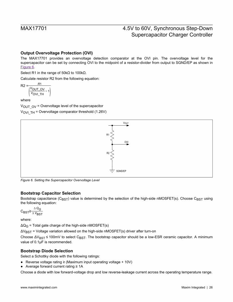
Output Overvoltage Protection (OVI)The MAX17701 provides an overvoltage detection comparator at the OVI pin. The overvoltage level for thesupercapacitor can be set by connecting OVI to the midpoint of a resistor-divider from output to SGND/EP as shown inFigure 6.Select R1 in the range of 50kΩ to 100kΩ.Calculate resistor R2 from the following equation:
R2 = R1
(VOUT_OVVOVI_TH
− 1)whereVOUT_OV = Overvoltage level of the supercapacitorVOVI_TH = Overvoltage comparator threshold (1.26V)
SGND/EP
R1
R2
VOUT
OVI
Figure 6. Setting the Supercapacitor Overvoltage Level
Bootstrap Capacitor SelectionBootstrap capacitance (CBST) value is determined by the selection of the high-side nMOSFET(s). Choose CBST usingthe following equation:
CBST≥∆ QG
∆ VBST
where:ΔQG = Total gate charge of the high-side nMOSFET(s)ΔVBST = Voltage variation allowed on the high-side nMOSFET(s) driver after turn-onChoose ΔVBST ≤ 100mV to select CBST. The bootstrap capacitor should be a low-ESR ceramic capacitor. A minimumvalue of 0.1μF is recommended.
Bootstrap Diode SelectionSelect a Schottky diode with the following ratings: Reverse voltage rating ≥ (Maximum input operating voltage + 10V) Average forward current rating ≥ 1AChoose a diode with low forward-voltage drop and low reverse-leakage current across the operating temperature range.
MAX17701 4.5V to 60V, Synchronous Step-DownSupercapacitor Charger Controller
www.maximintegrated.com Maxim Integrated | 26
Input Short-Circuit Protection External nMOSFET SelectionThe MAX17701 is designed to control an external logic level nMOSFET that turns Off in less than 100ns and isolatesthe VIN node from input short-circuit events. This feature prevents discharge of the supercapacitor into the input duringinput (DCIN) short-circuit events. The external nMOSFET used for this feature only turns On once during power-upand turns Off during shutdown; therefore, the nMOSFET does not need to be optimized for switching performance.This external nMOSFET should therefore be selected with low RDS-On for low forward path conduction losses. TheMAX17701 supports external nMOSFETs with gate charge up to 250nC at VGS = 3.9V. Using larger values results in agate charging time larger than 15ms (tGATEN_OK) and causes the MAX17701 to enter a latched Fault condition.
Step-Down Converter nMOSFET SelectionThe MAX17701 drives two external logic-level nMOSFETs to implement the step-down converter high-side and low-sideswitches. These nMOSFETs must be logic-level compatible with guaranteed on-resistance specifications provided atVGS = 4.5V. The key selection parameters to choose these MOSFETs include: On-resistance (RDS-ON) Maximum drain-to-source voltage (VDS(MAX)) Miller Plateau voltage on the nMOSFET Gate (VMIL) Total gate charge (QG) Output capacitance (COSS) Power-dissipation rating and package thermal resistance Maximum operating junction temperatureFor the step-down converter, nMOSFETs should be chosen in such a way that the switching losses and conductionlosses are balanced and optimized. The duty cycles for the high-side and low-side external nMOSFETs can be calculatedas follows:
D =VOUT
VIN
High-side nMOSFET duty cycle: DLow-side nMOSFET duty cycle: 1 - DHigh-side nMOSFET losses can be estimated using the following formula:PHS-MOSFET = PHS-MOSFET_CONDUCTION + PHS-MOSFET_SWITCHING
where:fSW = Switching frequencyICHG = Charging currentQSW = Switching charge of the high-side nMOSFET from the nMOSFET data sheet,RDR = Sum of the DH pin driver pullup resistance and the high-side nMOSFET internal gate resistance,VMIL = VGS of the high-side nMOSFET that corresponds to ID = ICHGMAX on the VGS vs. ID curve in the nMOSFET datasheetQrr = Reverse-recovery charge of low-side nMOSFET(s) body diodeCOSSHS = Effective output capacitance of the high-side nMOSFET(s)COSSLS = Effective output capacitance of the low-side nMOSFET(s)Low-side nMOSFET losses can be estimated using the following formula:
MAX17701 4.5V to 60V, Synchronous Step-DownSupercapacitor Charger Controller
www.maximintegrated.com Maxim Integrated | 27
VD = Forward-drop of the low-side nMOSFET(s) body diodetDT = Dead time (30ns)Take RDS-ON variation with respect to temperature into account while calculating the power losses and ensure thatthe losses of each nMOSFET do not exceed their power rating and operate within a safe junction temperature rating.When parallel nMOSFETs are used, it is recommended to use appropriate independent series gate resistors for eachnMOSFET to account for gate charge variation from one nMOSFET to another.
Device Power DissipationThe MAX17701 must dissipate losses due to quiescent current consumption and the internal gate driver.If VCC is powered from VIN, use the following equation to calculate the approximate IC losses:
PMAX17701 = VIN × [[QG × fSW] + IQNS]When VOUT is used to power VCC by connecting the EXTVCC pin to an output voltage greater than 4.8V, use thefollowing equation to calculate the approximate IC losses:
PMAX17701=VEXTVCC × [[QG × fSW] + IQNS]where:QG = Total gate charge of high-side and low-side nMOSFETs,IQNS = Input Quiescent current (2.1mA)
Calculate the junction temperature using the following equation and ensure that it does not exceed +125°C.
TJ = TA(MAX) + (θJA × PMAX17701)where:TJ = Junction temperaturePMAX17701 = Power loss in the deviceθJA = Junction-to-ambient thermal resistanceTA(MAX) = Maximum ambient temperature
PCB Layout GuidelinesCareful PCB layout is critical to achieve low losses and low EMI emissions. Use the following guidelines for PCB layout: Place ceramic input filter capacitors as close as possible across the drain of the high-side nMOSFET and source of
the low-side nMOSFET. Route the VIN and DCIN traces from input short-circuit protection nMOSFET source and drain terminals as a
differential pair and connect to VIN and DCIN pins of the device. Place VIN and DCIN bypass capacitors close to VINand DCIN pins, respectively.
Place VCC and EXTVCC bypass capacitors and the BST capacitor near the respective pins. Place GATEN-to-DCIN bypass capacitor close to the GATEN, DCIN pins of the device. Place the bootstrap capacitor close to the BST and LX pins of the device. Route the bootstrap diode connections from the VCC capacitor and to the bootstrap capacitor as short as possible to
minimize the loop inductance. Route switching traces (BST, LX, DH, and DL) away from sensitive signal traces (RT/SYNC, COMP, CSP, CSN and
FB). The gate current traces must be short in length. Use multiple vias to route these signals if routed from one layer of the
PCB to another layer. Route current-sense traces as a differential pair to minimize the loop inductance and avoid differential noise. Place a current-sense filter resistor and capacitor near the CSP and CSN pins. Place feedback and compensation components close to the device and connect to the SGND/EP copper area.
MAX17701 4.5V to 60V, Synchronous Step-DownSupercapacitor Charger Controller
www.maximintegrated.com Maxim Integrated | 28
Place all power components on the top side of the board and run the power-stage currents using traces or copper fillson the top side only without adding vias wherever possible.
Keep the power traces and load connections short. Use multilayer, thick copper PCBs (2oz or higher) to enhanceefficiency and minimize trace inductance and resistance.
Allocate a large PGND copper area for the output node and connect the return terminals of the input filter capacitors,output capacitors, and the source terminals of the low-side nMOSFET(s) to that area.
Refer to the MAX17701 EV kit data sheet for recommended PCB layout and routing.
MAX17701 4.5V to 60V, Synchronous Step-DownSupercapacitor Charger Controller
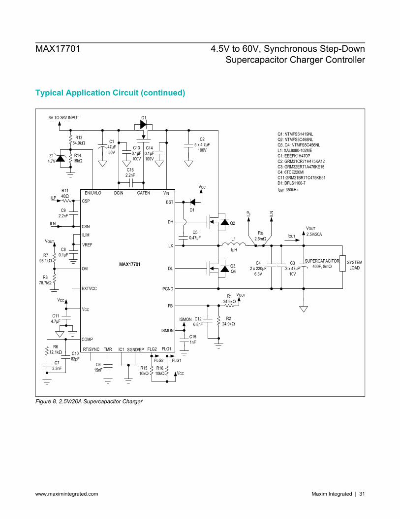
MAX17701 4.5V to 60V, Synchronous Step-DownSupercapacitor Charger Controller
www.maximintegrated.com Maxim Integrated | 31
Ordering InformationPART NUMBER TEMPERATURE RANGE PIN-PACKAGEMAX17701ATG+ -40ºC to +125ºC 24 TQFN-EP
MAX17701ATG+T -40ºC to +125ºC 24 TQFN-EP
+ Denotes a lead(Pb)-free/RoHS-compliant package.T Denotes tape-and-reel.
MAX17701 4.5V to 60V, Synchronous Step-DownSupercapacitor Charger Controller
www.maximintegrated.com Maxim Integrated | 32
Revision HistoryREVISIONNUMBER
REVISIONDATE DESCRIPTION PAGES
CHANGED0 4/20 Initial release —
1 6/20
Updated the General Description, Benefit and Features, Simplified ApplicationCircuit, Absolute Maximum Ratings, Electrical Characteristics, Detailed Description,Operating Input-Voltage Range, CC Mode Charging Current Settings (ILIM), Step-Down Converter nMOSFET Selection, and Typical Application Circuit (Figures 7 and8) sections
1–2, 6, 13,21–23,
27, 29–30
2 11/20Updated the Pin Description, Charger Timers, PCB Layout Guidelines and TypicalApplication Circuit (Figures 7 and 8) sections, and Table 1; replaced TOC01 withnew TOC01a and TOC01b in the Typical Operating Characteristics section
8, 11, 17–18,27–29
3 3/21
Updated the General Description, Benefits and Features, Simplified ApplicationCircuit, Absolute Maximum Ratings, Electrical Characteristics, Pin Configuration, PinDescription, MAX17701 Block Diagram, Detailed Description, Power-Up/-DownSequence, Input Short-Circuit Protection (GATEN), Charger Operation, ChargerTimers (TMR), Hardware Faults, Linear Regulator (VCC and EXTVCC), PeakCurrent-Limit, Inductor Selection, Operating Input-Voltage Range, CC ModeCharging Current Setting (ILIM), PCB Layout Guidelines, and the Typical ApplicationCircuit sections; updated TOC14 in Typical Operating Characteristics section; addedthe Charger Status Outputs (FLG1, FLG2) and Bootstrap Diode Selection sections
1–2, 4–6, 9,11–24, 26–27,
29–31
For pricing, delivery, and ordering information, please visit Maxim Integrated’s online storefront at https://www.maximintegrated.com/en/storefront/storefront.html.
Maxim Integrated cannot assume responsibility for use of any circuitry other than circuitry entirely embodied in a Maxim Integrated product. No circuit patentlicenses are implied. Maxim Integrated reserves the right to change the circuitry and specifications without notice at any time. The parametric values (min and maxlimits) shown in the Electrical Characteristics table are guaranteed. Other parametric values quoted in this data sheet are provided for guidance.
MAX17701 4.5V to 60V, Synchronous Step-DownSupercapacitor Charger Controller