42
CM-T335 CoM Reference Guide
CM-T335 CoM
Reference Guide
Introduction
Revised March 2016 CM-T335 Reference Guide 2
© 2014 CompuLab Ltd.
All Rights Reserved. No part of this document may be photocopied, reproduced, stored in a retrieval
system, or transmitted, in any form or by any means whether, electronic, mechanical, or otherwise
without the prior written permission of CompuLab Ltd..
No warranty of accuracy is given concerning the contents of the information contained in this
publication. To the extent permitted by law no liability (including liability to any person by reason of
negligence) will be accepted by CompuLab Ltd., its subsidiaries or employees for any direct or
indirect loss or damage caused by omissions from or inaccuracies in this document.
CompuLab Ltd. reserves the right to change details in this publication without notice.
Product and company names herein may be the trademarks of their respective owners.
CompuLab Ltd.
Ha-Yetzira 17, Yokneam Ilit
26290, Israel
Tel: +972 (4) 8290100
http://www.compulab.co.il
Fax: +972 (4) 8325251
Table of Contents
Revised March 2016 CM-T335 Reference Guide 3
Table of Contents
1 INTRODUCTION .............................................................................................................. 6
1.1 About This Document ...................................................................................................... 6
1.2 CM-T335 Part Number Legend ....................................................................................... 6
1.3 Related Documents .......................................................................................................... 6
2 OVERVIEW ........................................................................................................................ 7
2.1 Highlights ......................................................................................................................... 7
2.2 Block Diagram ................................................................................................................. 8
2.3 CM-T335 Features ........................................................................................................... 9
3 CORE SYSTEM COMPONENTS .................................................................................. 10
3.1 AM335x SoC ................................................................................................................. 10
3.2 Graphics Subsystem ....................................................................................................... 10
3.3 Memory .......................................................................................................................... 10
3.3.1 DRAM ................................................................................................................... 10
3.3.2 Storage .................................................................................................................. 10
4 PERIPHERAL INTERFACES ....................................................................................... 11
4.1 LCD Interface................................................................................................................. 12
4.2 Audio Subsystem ........................................................................................................... 13
4.2.1 Analog Audio ........................................................................................................ 13
4.2.1 Digital Audio ........................................................................................................ 14
4.3 WLAN and Bluetooth .................................................................................................... 15
4.4 Ethernet .......................................................................................................................... 17
4.4.1 Ethernet PHY ........................................................................................................ 17
4.4.2 RGMII Interface .................................................................................................... 18
4.5 USB 2.0 .......................................................................................................................... 19
4.5.1 USB 2.0 On-The-Go ............................................................................................. 19
4.5.2 USB 2.0 Hub ......................................................................................................... 19
4.6 UART ............................................................................................................................. 20
4.7 MMC / SD / SDIO ......................................................................................................... 21
4.8 ADC / Touch-Screen ...................................................................................................... 23
4.9 GPIO .............................................................................................................................. 23
4.10 I2C .............................................................................................................................. 25
4.11 SPI ............................................................................................................................. 26
4.12 CAN BUS .................................................................................................................. 27
4.13 JTAG ......................................................................................................................... 27
5 SYSTEM LOGIC .............................................................................................................. 28
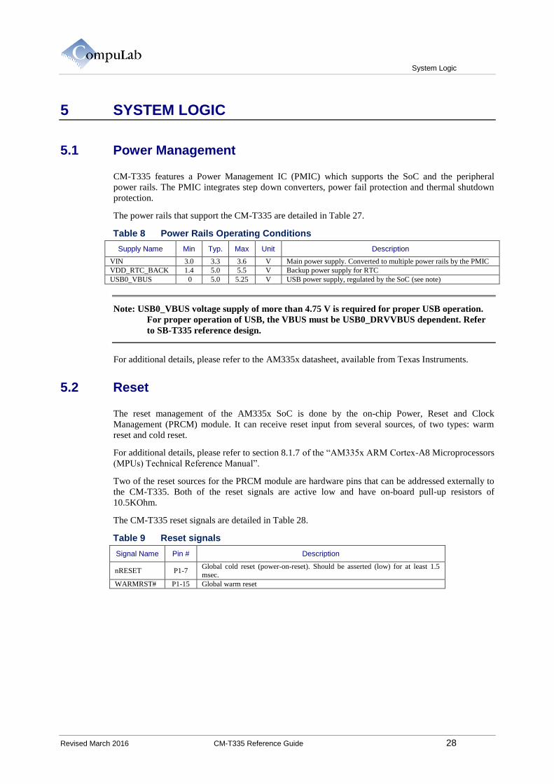
5.1 Power Management ........................................................................................................ 28
5.2 Reset ............................................................................................................................... 28
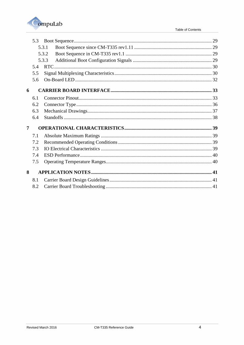
Table of Contents
Revised March 2016 CM-T335 Reference Guide 4
5.3 Boot Sequence ................................................................................................................ 29
5.3.1 Boot Sequence since CM-T335 rev1.11 ............................................................... 29
5.3.2 Boot Sequence in CM-T335 rev1.1 ...................................................................... 29
5.3.3 Additional Boot Configuration Signals ................................................................ 29
5.4 RTC ................................................................................................................................ 30
5.5 Signal Multiplexing Characteristics ............................................................................... 30
5.6 On-Board LED ............................................................................................................... 32
6 CARRIER BOARD INTERFACE .................................................................................. 33
6.1 Connector Pinout ............................................................................................................ 33
6.2 Connector Type .............................................................................................................. 36
6.3 Mechanical Drawings..................................................................................................... 37
6.4 Standoffs ........................................................................................................................ 38
7 OPERATIONAL CHARACTERISTICS ....................................................................... 39
7.1 Absolute Maximum Ratings .......................................................................................... 39
7.2 Recommended Operating Conditions ............................................................................ 39
7.3 IO Electrical Characteristics .......................................................................................... 39
7.4 ESD Performance ........................................................................................................... 40
7.5 Operating Temperature Ranges...................................................................................... 40
8 APPLICATION NOTES .................................................................................................. 41
8.1 Carrier Board Design Guidelines ................................................................................... 41
8.2 Carrier Board Troubleshooting ...................................................................................... 41
Revision Information
Revised March 2016 CM-T335 Reference Guide 5
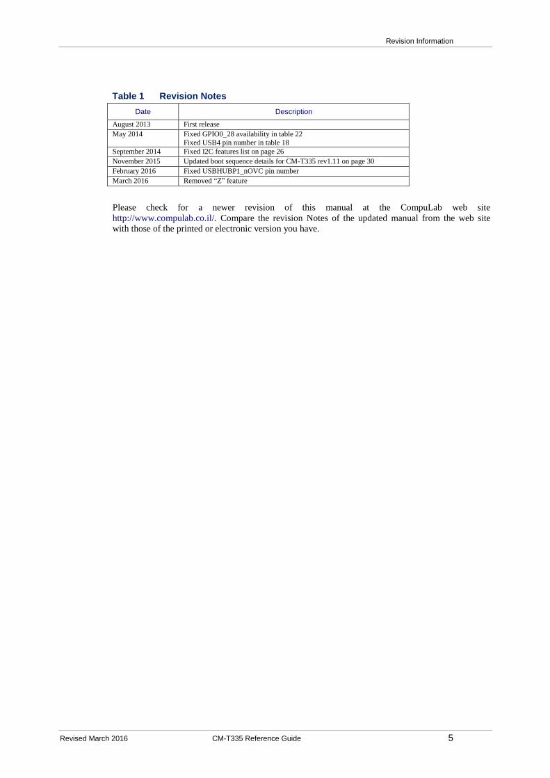
Table 1 Revision Notes
Date Description
August 2013 First release
May 2014 Fixed GPIO0_28 availability in table 22
Fixed USB4 pin number in table 18
September 2014 Fixed I2C features list on page 26
November 2015 Updated boot sequence details for CM-T335 rev1.11 on page 30
February 2016 Fixed USBHUBP1_nOVC pin number
March 2016 Removed “Z” feature
Please check for a newer revision of this manual at the CompuLab web site
http://www.compulab.co.il/. Compare the revision Notes of the updated manual from the web site
with those of the printed or electronic version you have.
Introduction
Revised March 2016 CM-T335 Reference Guide 6
1 INTRODUCTION
1.1 About This Document
This document is part of a set of reference documents providing information necessary to operate and
program CompuLab CM-T335 Computer-on-Module.
1.2 CM-T335 Part Number Legend
Please refer to the CompuLab website ‘Ordering information’ section to decode the CM-T335 part
number: http://compulab.co.il/products/computer-on-modules/cm-t335/#ordering.
1.3 Related Documents
For additional information, refer to the documents listed in Table 2.
Table 2 Related Documents
Document Location
CM-T335 Developer Resources http://www.compulab.com/
AM335x Technical Reference Manual http://www.ti.com/
AM335x Datasheet http://www.ti.com/
Overview
Revised March 2016 CM-T335 Reference Guide 7
2 OVERVIEW
2.1 Highlights
Texas Instruments Cortex-A8 Sitara AM3352 / AM3354 SoC, up to 600MHz
Up to 512MB DDR3
Up to 1GB NAND storage
Display controller with support of up to WXGA (1366 x 768) resolution
PowerVR SGX GPU with OpenGL-ES and OpenVG support
Gigabit Ethernet, USB2.0 x4, UART x6, GPIO x65, SDIO x3, SPI x2, I2C x3, CAN
Wi-Fi 802.11b/g/n and Bluetooth 4.0
Analog audio, touch-screen, ADC
Linux, Android and Windows Embedded Compact 7
Tiny size: 68 x 30 x 5 mm
SB-T335 carrier board turns the CM-T335 module into SBC-T335 - a tiny single board
computer
Overview
Revised March 2016 CM-T335 Reference Guide 8
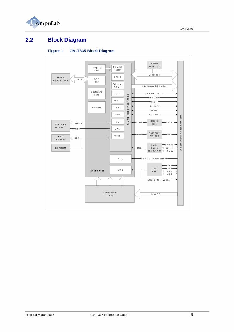
2.2 Block Diagram
Figure 1 CM-T335 Block Diagram
L in e o u t
N A N D
U p to 1 G B
D D R 3
U p to 5 1 2 M B
20
4-p
in S
OD
IMM
ed
ge
co
nn
ec
tor
A M 3 3 5 x
G b E P H Y
A R 8 0 3 3
U S BU S B
h u b
T P S 6 5 0 2 5 0
P M IC
D D R
C tr l.
1 6 b it
A u d io
C o d e c
T L V 3 2 0 A IC
D is p la y
C tr l.
2 4 -b it p a ra lle l d is p la y
G P M C
I2 S
E th e rn e t
R G M II
L o c a l b u s
M M C
P a ra lle l
d is p la y
U A R T
S P I
I2 C
C A N
G P IO
R S 2 3 2
x c v r .
3 x M M C / S D IO
6 5 x G P IO
2 x S P I
2 x C A N
6 x U A R T
R S 2 3 2
G b ER G M II
L in e in
M ic in
I2 S
A D C 8 x A D C / to u c h -s c re e n
U S B
U S B
U S B
U S B
C o rte x -A 8
c o re
S G X 5 3 0
W iF i + B T
W L 1 2 7 1 LS P I
U A R T
3 x I2 C
R T C
E M 3 0 2 7
E E P R O M
I2 C
3 .3 V D C
U S B O T G (b y p a s s )
Mu
ltip
lex
ed
in
terf
ac
es
U A R T
Overview
Revised March 2016 CM-T335 Reference Guide 9
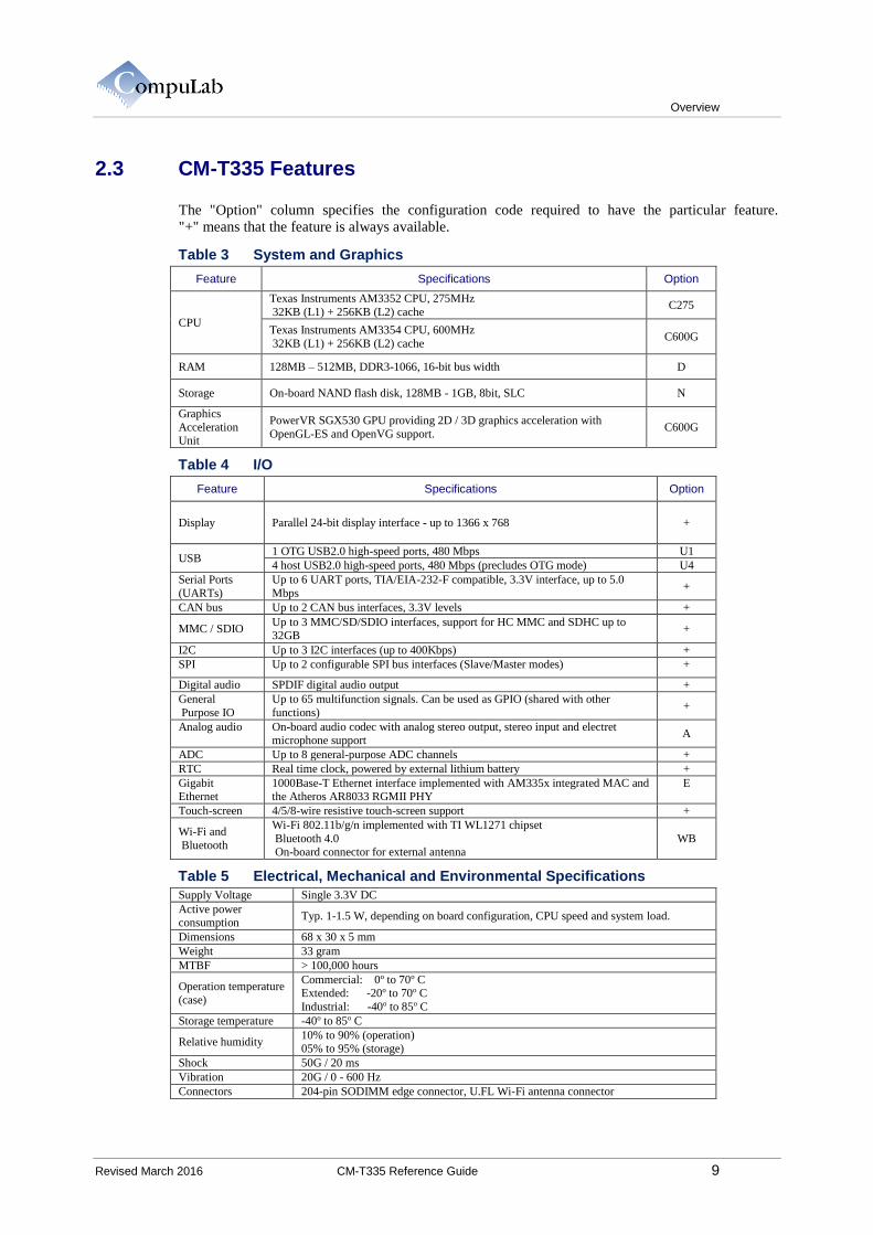
2.3 CM-T335 Features
The "Option" column specifies the configuration code required to have the particular feature.
"+" means that the feature is always available.
Table 3 System and Graphics
Feature Specifications Option
CPU
Texas Instruments AM3352 CPU, 275MHz
32KB (L1) + 256KB (L2) cache C275
Texas Instruments AM3354 CPU, 600MHz
32KB (L1) + 256KB (L2) cache C600G
RAM 128MB – 512MB, DDR3-1066, 16-bit bus width D
Storage On-board NAND flash disk, 128MB - 1GB, 8bit, SLC N
Graphics
Acceleration Unit
PowerVR SGX530 GPU providing 2D / 3D graphics acceleration with
OpenGL-ES and OpenVG support. C600G
Table 4 I/O
Feature Specifications Option
Display Parallel 24-bit display interface - up to 1366 x 768 +
USB 1 OTG USB2.0 high-speed ports, 480 Mbps U1
4 host USB2.0 high-speed ports, 480 Mbps (precludes OTG mode) U4
Serial Ports
(UARTs)
Up to 6 UART ports, TIA/EIA-232-F compatible, 3.3V interface, up to 5.0
Mbps +
CAN bus Up to 2 CAN bus interfaces, 3.3V levels +
MMC / SDIO Up to 3 MMC/SD/SDIO interfaces, support for HC MMC and SDHC up to 32GB
+
I2C Up to 3 I2C interfaces (up to 400Kbps) +
SPI Up to 2 configurable SPI bus interfaces (Slave/Master modes) +
Digital audio SPDIF digital audio output +
General
Purpose IO
Up to 65 multifunction signals. Can be used as GPIO (shared with other
functions) +
Analog audio On-board audio codec with analog stereo output, stereo input and electret microphone support
A
ADC Up to 8 general-purpose ADC channels +
RTC Real time clock, powered by external lithium battery +
Gigabit Ethernet
1000Base-T Ethernet interface implemented with AM335x integrated MAC and the Atheros AR8033 RGMII PHY
E
Touch-screen 4/5/8-wire resistive touch-screen support +
Wi-Fi and
Bluetooth
Wi-Fi 802.11b/g/n implemented with TI WL1271 chipset
Bluetooth 4.0
On-board connector for external antenna
WB
Table 5 Electrical, Mechanical and Environmental Specifications
Supply Voltage Single 3.3V DC
Active power consumption
Typ. 1-1.5 W, depending on board configuration, CPU speed and system load.
Dimensions 68 x 30 x 5 mm
Weight 33 gram
MTBF > 100,000 hours
Operation temperature
(case)
Commercial: 0o to 70o C Extended: -20o to 70o C
Industrial: -40o to 85o C
Storage temperature -40o to 85o C
Relative humidity 10% to 90% (operation) 05% to 95% (storage)
Shock 50G / 20 ms
Vibration 20G / 0 - 600 Hz
Connectors 204-pin SODIMM edge connector, U.FL Wi-Fi antenna connector

Core system components
Revised March 2016 CM-T335 Reference Guide 10
3 CORE SYSTEM COMPONENTS
3.1 AM335x SoC
AM335x SoC manufactured by Texas Instruments provides up to 600 MHz Sitara™ ARM®
Cortex™-A8 32-bit RISC CPU. It supports the following main features:
NEON™ SIMD Coprocessor
32 KB of L1 Data and 32 KB of L1 Instruction Cache
256 KB of L2 Cache with ECC
SGX530 3D Graphics Engine
Programmable Real-Time Unit and Industrial Communication Subsystem (PRU-ICSS)
USB 2.0 High-Speed OTG port with Integrated PHY
1000 Mbps Ethernet MAC controller
3.2 Graphics Subsystem
The AM335x 2D and 3D graphics accelerator (SGX) provides support for the following imaging and
video features:
2D and 3D graphics, vector graphics, and programming support for GP-GPU functions
Tile-based architecture
An advanced shader feature set in excess of Microsoft VS3.0, PS3.0 and OGL2.0
Industry standard API supports Direct3D mobile, OGL-ES 1.1 and 2.0, OpenVG 1.0.1 and
OpenMax
Fine-grained task switching, load balancing and power management
Programmable high-quality image anti-aliasing
Advanced geometry DMA driven operation for minimum CPU interaction
Fully virtualized memory addressing for OS operation in a unified memory architecture
NOTE: Graphics sub-system is available only with the ‘C600G’ configuration option.
3.3 Memory
3.3.1 DRAM
CM-T335 is available with up to 512MB of DDR3. The DDR3 interface is 16-bits wide and operates
at up to 303 MHz clock frequencies.
3.3.2 Storage
CM-T335 is equipped with up to 1GB of SLC NAND flash, which serves as the main non-volatile
storage of CM-T335. This storage is used for storing the system boot-loader and the OS. The NAND
identification begins with Open NAND Flash Interface (ONFI), according to the ONFI standard
specification.

Peripheral Interfaces
Revised March 2016 CM-T335 Reference Guide 11
4 PERIPHERAL INTERFACES
CM-T335 implements a number of peripheral interfaces through the carrier board interface connector.
The following notes apply to those interfaces:
Some interfaces/signals are available only with/without certain configuration options of the
CM-T335 CoM. Each signal availability is noted in the “Signals description” or "Availability"
column of each interface.
Many of the CM-T335 carrier board interface pins are multifunctional. Up-to 8 functions
(ALT modes) are accessible through each multifunctional pin. Multifunctional pins are
denoted with an asterisk (*). For additional details, please refer to chapter 5.5.
Only one multifunctional pin can be used for each function, configuring several
multifunctional pins to implement the same function will result in unexpected system
behavior.
All of CM-T335 digital interfaces operate at 3.3V voltage levels, unless otherwise noted.
The signals for each interface are described in the “Signal description” tables. The following Notes
summarize the column headers for these tables:
“Signal name” – The name of each signal with regards to the discussed interface. The signal
name corresponds to the relevant function in cases where the carrier board pin in question is
multifunctional.
“Pin#” – The carrier board interface pin number where the discussed signal is available,
multifunctional pins are denoted with an asterisk.
“Type” – Signal type, see the definition of different signal types below.
“Description” – Signal description with regards to the interface in question.
“Availability” – Depending on CM-T335 configuration options, certain carrier board interface
pins are physically disconnected (floating) on-board the CM-T335. The “Availability” column
summarizes configuration requirements for each signal. All the listed requirements must be
met (logical AND) for a signal to be “available” unless otherwise stated.
Each described signal can be one of the following types. Signal type is noted in the “Signal
description” tables. Multifunctional pin direction, pull resistor and open drain functionality is
software controlled. The “Type” column header for multifunctional pins refers to the recommended
pin configuration with regards to the discussed signal.
“AI” – Analog Input
“AO” – Analog Output
“AIO” – Analog Input/Output
“AP” – Analog Power Output
“I” – Digital Input
"O" – Digital Output
“IO” – Digital Input/Output
“OD” – Open Drain Signal (not pulled up on-board the CM-T335 unless otherwise noted).
“P” – Power
“SPU” – Software controlled pull up to 3.3V
“SPD” – Software controlled pull down to 3.3V
"PU33" – Always pulled up to 3.3V on-board the CM-T335, (typ. 5KΩ-15KΩ).
"PD" - Always pulled down on-board the CM-T335, (typ. 5KΩ-15KΩ).
Peripheral Interfaces
Revised March 2016 CM-T335 Reference Guide 12
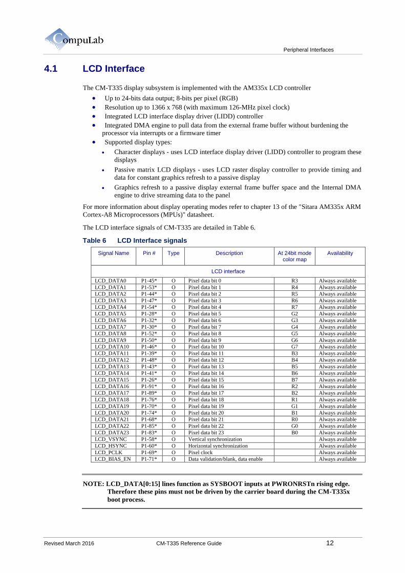
4.1 LCD Interface
The CM-T335 display subsystem is implemented with the AM335x LCD controller
Up to 24-bits data output; 8-bits per pixel (RGB)
Resolution up to 1366 x 768 (with maximum 126-MHz pixel clock)
Integrated LCD interface display driver (LIDD) controller
Integrated DMA engine to pull data from the external frame buffer without burdening the
processor via interrupts or a firmware timer
Supported display types:
Character displays - uses LCD interface display driver (LIDD) controller to program these
displays
Passive matrix LCD displays - uses LCD raster display controller to provide timing and
data for constant graphics refresh to a passive display
Graphics refresh to a passive display external frame buffer space and the Internal DMA
engine to drive streaming data to the panel
For more information about display operating modes refer to chapter 13 of the "Sitara AM335x ARM
Cortex-A8 Microprocessors (MPUs)" datasheet.
The LCD interface signals of CM-T335 are detailed in Table 6.
Table 6 LCD Interface signals
NOTE: LCD_DATA[0:15] lines function as SYSBOOT inputs at PWRONRSTn rising edge.
Therefore these pins must not be driven by the carrier board during the CM-T335x
boot process.
Signal Name Pin # Type Description At 24bit mode color map
Availability
LCD interface
LCD_DATA0 P1-45* O Pixel data bit 0 R3 Always available
LCD_DATA1 P1-53* O Pixel data bit 1 R4 Always available
LCD_DATA2 P1-44* O Pixel data bit 2 R5 Always available
LCD_DATA3 P1-47* O Pixel data bit 3 R6 Always available
LCD_DATA4 P1-54* O Pixel data bit 4 R7 Always available
LCD_DATA5 P1-28* O Pixel data bit 5 G2 Always available
LCD_DATA6 P1-32* O Pixel data bit 6 G3 Always available
LCD_DATA7 P1-30* O Pixel data bit 7 G4 Always available
LCD_DATA8 P1-52* O Pixel data bit 8 G5 Always available
LCD_DATA9 P1-50* O Pixel data bit 9 G6 Always available
LCD_DATA10 P1-46* O Pixel data bit 10 G7 Always available
LCD_DATA11 P1-39* O Pixel data bit 11 B3 Always available
LCD_DATA12 P1-48* O Pixel data bit 12 B4 Always available
LCD_DATA13 P1-43* O Pixel data bit 13 B5 Always available
LCD_DATA14 P1-41* O Pixel data bit 14 B6 Always available
LCD_DATA15 P1-26* O Pixel data bit 15 B7 Always available
LCD_DATA16 P1-91* O Pixel data bit 16 R2 Always available
LCD_DATA17 P1-89* O Pixel data bit 17 B2 Always available
LCD_DATA18 P1-76* O Pixel data bit 18 R1 Always available
LCD_DATA19 P1-70* O Pixel data bit 19 G1 Always available
LCD_DATA20 P1-74* O Pixel data bit 20 B1 Always available
LCD_DATA21 P1-68* O Pixel data bit 21 R0 Always available
LCD_DATA22 P1-85* O Pixel data bit 22 G0 Always available
LCD_DATA23 P1-83* O Pixel data bit 23 B0 Always available
LCD_VSYNC P1-58* O Vertical synchronization Always available
LCD_HSYNC P1-60* O Horizontal synchronization Always available
LCD_PCLK P1-69* O Pixel clock Always available
LCD_BIAS_EN P1-71* O Data validation/blank, data enable Always available

Peripheral Interfaces
Revised March 2016 CM-T335 Reference Guide 13
NOTE: Data bits have different color maps in different bit modes. For more information refer
to “Sitara™ AM335x ARM® Cortex™-A8 Microprocessors (MPUs) Silicon Revisions
2.1, 2.0, 1.0” Paragraph 3.1.1.
NOTE: Pins denoted with "*" are multifunctional. For details, please refer to section 5.5 of this
document.
4.2 Audio Subsystem
4.2.1 Analog Audio
CM-T355 analog audio subsystem is implemented with the Texas Instruments TLV320AIC23b audio
codec. The audio subsystem supports the following features:
Single ended stereo-line output
Single ended stereo-line input
Integrated total electret-microphone biasing and buffering solution
8-kHz – 96-kHz Sampling-Frequency Support
100-dB SNR Multibit Sigma-Delta DAC (A-weighted at 48 kHz)
90-dB SNR Multibit Sigma-Delta ADC (A-weighted at 48 kHz)
Audio signals characteristics are detailed in Table 7.
Table 7 Analog Audio Characteristics
Parameter Test conditions Min Typ Max Unit
Headphone Output
0-dB full-scale output voltage 1.0 VRMS
Maximum output power, PO Rload = 32Ω 30
Rload = 16Ω 40
Signal-to-noise ratio, A-weighted
(see Note 2)
90 97 dB
Total harmonic distortion 1kHz output Pout = 10mW 0.1 %
Pout = 20mW 1.0 %
Power supply rejection ratio 1 kHz, 100 mVp-p 50 dB
Programmable gain 1 kHz output -73 6
Programmable-gain step size 1
Mute attenuation 1 kHz output 80
Line Input to ADC
Input signal level (0 dB) 1.0 VRMS
Signal-to-noise ratio, A-weighted,
0-dB gain (see Notes 1 and 2) Fsample = 48 kHz.
85 90 dB
Dynamic range, A-weighted, −60-
dB full-scale input (see Note 2)
85 90 dB
Total harmonic distortion, −1-dB input, 0-dB gain
-80 dB
Power supply rejection ratio 1 kHz, 100 mVp-p 50 dB
ADC Channel Separation 1 kHz input tone 90 dB
Programmable-gain step size Monotonic 1.5 dB
Mute attenuation 0dB, 1 kHz input tone 80 dB
Input resistance 12 dB input gain 10 20
kΩ 0 dB input gain 30 35
Input capacitance 10 pF
Microphone Input to ADC
Input signal level (0 dB) 1.0 VRMS
Peripheral Interfaces
Revised March 2016 CM-T335 Reference Guide 14
Signal-to-noise ratio, A-weighted,
0-dB gain (see Notes 1 and 2)
80 85 dB
Dynamic range, A-weighted, −60-dB full-scale input (see Note 2)
80 85 dB
Total harmonic distortion, −1-dB
input, 0-dB gain
-60 dB
Power supply rejection ratio 1 kHz, 100 mVp-p 50 dB
Mute attenuation 0dB, 1 kHz input tone 60 80 dB
Input resistance 8 14 kΩ
Input capacitance 10 pF
Microphone Bias
Bias voltage 2.375 2.475 2.575 V
Bias-current source 3 mA
For additional details, please refer to the TLV320AIC23B datasheet, available from Texas
Instruments.
Analog audio signals are detailed in Table 8.
Table 7 Analog Audio Signals
Signal Name Pin # Type Description Availability
AUDIO_OUT_R P1-137 AO Right channel headphone output
Only available with
‘A’ option.
AUDIO_OUT_L P1-135 AO Left channel headphone output
AUDIO_IN_R/MONO P1-166 AI Right channel line input
AUDIO_IN_L/MONO P1-168 AI Left channel line input
MIC_IN P1-147 AI Microphone input
MIC_BIAS P1-145 AP Electret microphone bias supply
4.2.1 Digital Audio
CM-T355 digital audio subsystem supports the following features:
S/PDIF transmit physical layer components.
Up to 384 subframes blocks.
S/PDIF, IEC60958-1, AES-3 formats.
TDM streams from 2 to 32 time slots.
The digital audio signals are detailed in Table 9.
Table 9 Digital Audio Signals
Signal Name Pin # Type Description Availability
McASP1_AXR2 P1-141* O S/PDIF transmit data Always available
MCASP_1AXR3 P1-157* O S/PDIF transmit data Always available
NOTE: Pins denoted with "*" are multifunctional. For details, please refer to section 5.5 of this
document.

Peripheral Interfaces
Revised March 2016 CM-T335 Reference Guide 15
4.3 WLAN and Bluetooth
CM-T335x incorporates full-featured 802.11b/g/n and Bluetooth 4.0 capabilities, implemented with
the Murata LBEH59XUHC WLAN + Bluetooth combo controller module. LBEH59XUHC is based
on the TI WiLink6.0 WL1271 chipset.
WLAN Standards supported:
802.11b data rates of 1, 2, 5.5 and 11 Mbps
802.11g data rates of 6, 9, 12, 18, 24, 36, 48, and 54 Mbps
802.11n-2.4G data rates of 6.5, 13, 19.5, 26, 39, 52, 58.5 and 65 Mbps
Bluetooth standards supported:
Bluetooth 4.0
Bluetooth Power Class 1
LBEH59XUHC SiP is interfaced with the Sitara AM335x SoC using the SPI and UART ports. SPI0
is used for WLAN data, while UART1 is used for Bluetooth data.
The LBEH59XUHC requires a single 2.45GHz antenna. The antenna is connected via the onboard
UFL high frequency connector J1. Refer to section 0 for antenna connector location.
The Wi-Fi antenna onboard and mating connector specifications are detailed in Table 10.
Table 10 J1 connector data
Manufacturer Mfg. P/N Mating Connector
Hirose U.FL-R-MT(10) Hirose U.FL-LP-040
The WLAN 802.11b/g/n and Bluetooth RF specifications are detailed in Tables 11, 12, 13 and 14.
Table 11 802.11b (WLAN) RF system specifications
TX Characteristics
Parameter Min Typ. Max Unit
Power Levels 14 16 18 dBm
Spectrum Mask
1st side lobes -40 -30 dBr
2nd side lobes -55 -50 dBr
Power-on and Power-down ramp 0.1 2 µSec
RF Carrier Suppression 15 37 dB
Modulation Accuracy (EVM) 10 35 %
Spurious Emissions
30MHz to 1GHz -80 -36 dBm
1GHz to 12.75GHz -60 -30 dBm
1.8GHz to 1.9GHz -80 -47 dBm
5.15GHz to 5.3GHz -80 -47 dBm
RX Characteristics
Parameter Min Typ. Max Unit
Minimum Input Level Sensitivity
11Mbps (FER ≤ 8%) -87 -76 dBm
Maximum Input Level (FER ≤ 8%) -10 0 dBm
Table 12 802.11g (WLAN) RF system specifications
TX Characteristics
Parameter Min Typ. Max Unit
Power Levels 11 13 15 dBm
Spectrum Mask
at fc +/- 11MHz -30 -20 dBr
at fc +/- 20MHz -33 -28 dBr
at fc +/- 30MHz -45 -40 dBr
Spurious Emissions
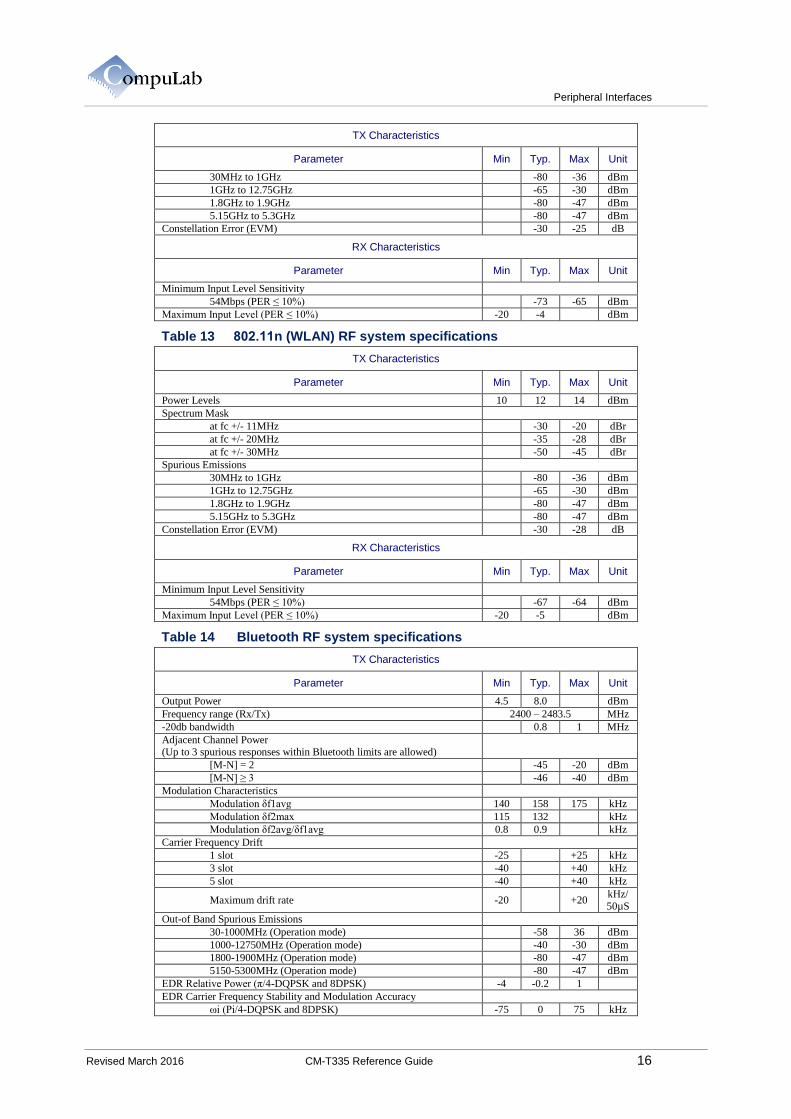
Peripheral Interfaces
Revised March 2016 CM-T335 Reference Guide 16
TX Characteristics
Parameter Min Typ. Max Unit
30MHz to 1GHz -80 -36 dBm
1GHz to 12.75GHz -65 -30 dBm
1.8GHz to 1.9GHz -80 -47 dBm
5.15GHz to 5.3GHz -80 -47 dBm
Constellation Error (EVM) -30 -25 dB
RX Characteristics
Parameter Min Typ. Max Unit
Minimum Input Level Sensitivity
54Mbps (PER ≤ 10%) -73 -65 dBm
Maximum Input Level (PER ≤ 10%) -20 -4 dBm
Table 13 802.11n (WLAN) RF system specifications
TX Characteristics
Parameter Min Typ. Max Unit
Power Levels 10 12 14 dBm
Spectrum Mask
at fc +/- 11MHz -30 -20 dBr
at fc +/- 20MHz -35 -28 dBr
at fc +/- 30MHz -50 -45 dBr
Spurious Emissions
30MHz to 1GHz -80 -36 dBm
1GHz to 12.75GHz -65 -30 dBm
1.8GHz to 1.9GHz -80 -47 dBm
5.15GHz to 5.3GHz -80 -47 dBm
Constellation Error (EVM) -30 -28 dB
RX Characteristics
Parameter Min Typ. Max Unit
Minimum Input Level Sensitivity
54Mbps (PER ≤ 10%) -67 -64 dBm
Maximum Input Level (PER ≤ 10%) -20 -5 dBm
Table 14 Bluetooth RF system specifications
TX Characteristics
Parameter Min Typ. Max Unit
Output Power 4.5 8.0 dBm
Frequency range (Rx/Tx) 2400 – 2483.5 MHz
-20db bandwidth 0.8 1 MHz
Adjacent Channel Power (Up to 3 spurious responses within Bluetooth limits are allowed)
[M-N] = 2 -45 -20 dBm
[M-N] ≥ 3 -46 -40 dBm
Modulation Characteristics
Modulation δf1avg 140 158 175 kHz
Modulation δf2max 115 132 kHz
Modulation δf2avg/δf1avg 0.8 0.9 kHz
Carrier Frequency Drift
1 slot -25 +25 kHz
3 slot -40 +40 kHz
5 slot -40 +40 kHz
Maximum drift rate -20
+20 kHz/50µS
Out-of Band Spurious Emissions
30-1000MHz (Operation mode) -58 36 dBm
1000-12750MHz (Operation mode) -40 -30 dBm
1800-1900MHz (Operation mode) -80 -47 dBm
5150-5300MHz (Operation mode) -80 -47 dBm
EDR Relative Power (π/4-DQPSK and 8DPSK) -4 -0.2 1
EDR Carrier Frequency Stability and Modulation Accuracy
ωi (Pi/4-DQPSK and 8DPSK) -75 0 75 kHz
Peripheral Interfaces
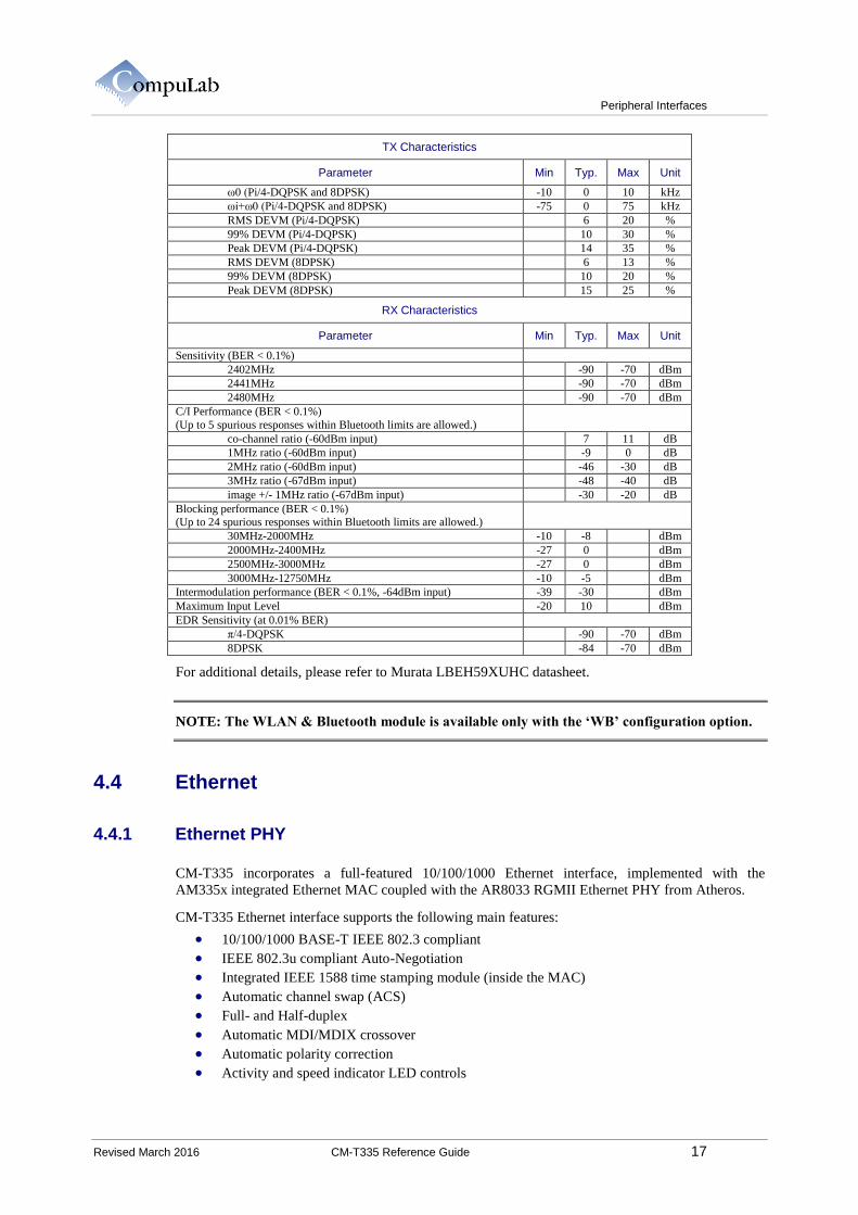
Revised March 2016 CM-T335 Reference Guide 17
TX Characteristics
Parameter Min Typ. Max Unit
ω0 (Pi/4-DQPSK and 8DPSK) -10 0 10 kHz
ωi+ω0 (Pi/4-DQPSK and 8DPSK) -75 0 75 kHz
RMS DEVM (Pi/4-DQPSK) 6 20 %
99% DEVM (Pi/4-DQPSK) 10 30 %
Peak DEVM (Pi/4-DQPSK) 14 35 %
RMS DEVM (8DPSK) 6 13 %
99% DEVM (8DPSK) 10 20 %
Peak DEVM (8DPSK) 15 25 %
RX Characteristics
Parameter Min Typ. Max Unit
Sensitivity (BER < 0.1%)
2402MHz -90 -70 dBm
2441MHz -90 -70 dBm
2480MHz -90 -70 dBm
C/I Performance (BER < 0.1%)
(Up to 5 spurious responses within Bluetooth limits are allowed.)
co-channel ratio (-60dBm input) 7 11 dB
1MHz ratio (-60dBm input) -9 0 dB
2MHz ratio (-60dBm input) -46 -30 dB
3MHz ratio (-67dBm input) -48 -40 dB
image +/- 1MHz ratio (-67dBm input) -30 -20 dB
Blocking performance (BER < 0.1%) (Up to 24 spurious responses within Bluetooth limits are allowed.)
30MHz-2000MHz -10 -8 dBm
2000MHz-2400MHz -27 0 dBm
2500MHz-3000MHz -27 0 dBm
3000MHz-12750MHz -10 -5 dBm
Intermodulation performance (BER < 0.1%, -64dBm input) -39 -30 dBm
Maximum Input Level -20 10 dBm
EDR Sensitivity (at 0.01% BER)
π/4-DQPSK -90 -70 dBm
8DPSK -84 -70 dBm
For additional details, please refer to Murata LBEH59XUHC datasheet.
NOTE: The WLAN & Bluetooth module is available only with the ‘WB’ configuration option.
4.4 Ethernet
4.4.1 Ethernet PHY
CM-T335 incorporates a full-featured 10/100/1000 Ethernet interface, implemented with the
AM335x integrated Ethernet MAC coupled with the AR8033 RGMII Ethernet PHY from Atheros.
CM-T335 Ethernet interface supports the following main features:
10/100/1000 BASE-T IEEE 802.3 compliant
IEEE 802.3u compliant Auto-Negotiation
Integrated IEEE 1588 time stamping module (inside the MAC)
Automatic channel swap (ACS)
Full- and Half-duplex
Automatic MDI/MDIX crossover
Automatic polarity correction
Activity and speed indicator LED controls
Peripheral Interfaces
Revised March 2016 CM-T335 Reference Guide 18
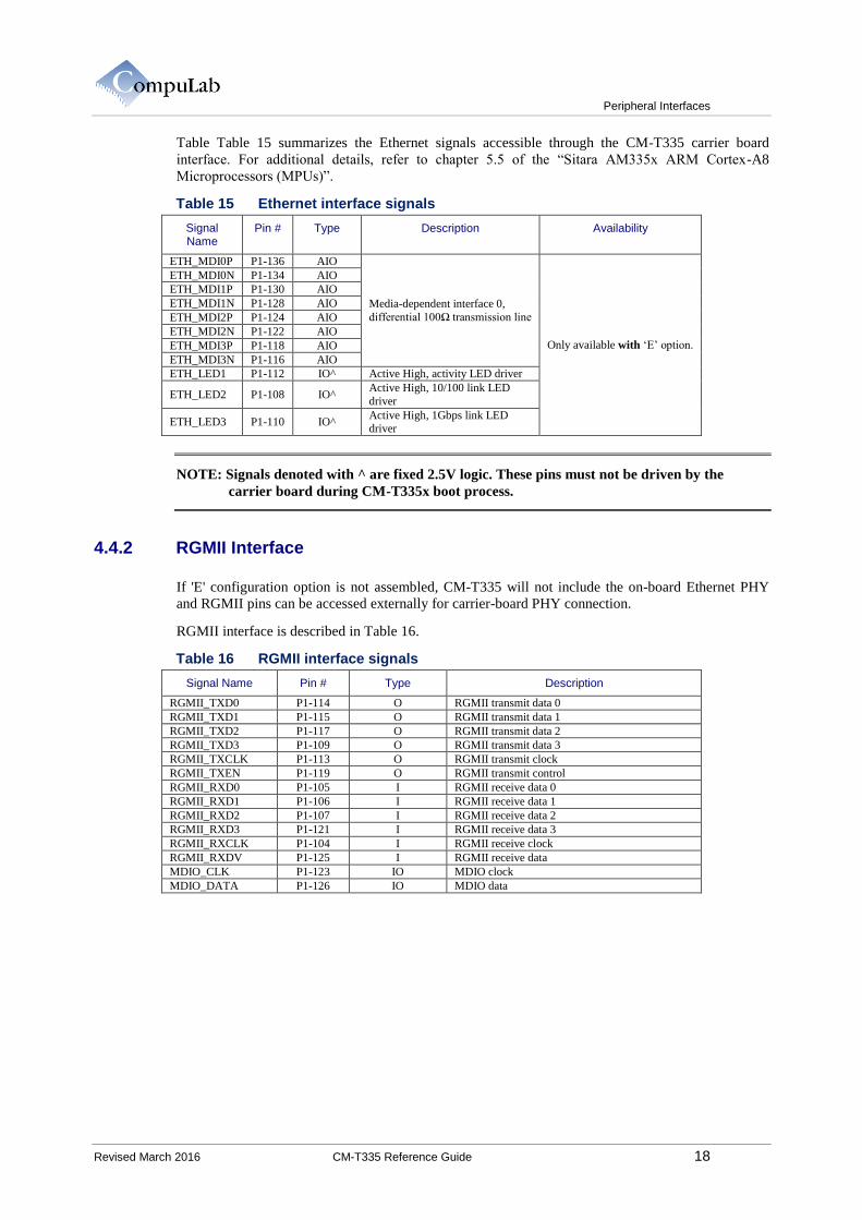
Table Table 15 summarizes the Ethernet signals accessible through the CM-T335 carrier board
interface. For additional details, refer to chapter 5.5 of the “Sitara AM335x ARM Cortex-A8
Microprocessors (MPUs)”.
Table 15 Ethernet interface signals
Signal Name
Pin # Type Description Availability
ETH_MDI0P P1-136 AIO
Media-dependent interface 0,
differential 100Ω transmission line
Only available with ‘E’ option.
ETH_MDI0N P1-134 AIO
ETH_MDI1P P1-130 AIO
ETH_MDI1N P1-128 AIO
ETH_MDI2P P1-124 AIO
ETH_MDI2N P1-122 AIO
ETH_MDI3P P1-118 AIO
ETH_MDI3N P1-116 AIO
ETH_LED1 P1-112 IO^ Active High, activity LED driver
ETH_LED2 P1-108 IO^ Active High, 10/100 link LED
driver
ETH_LED3 P1-110 IO^ Active High, 1Gbps link LED driver
NOTE: Signals denoted with ^ are fixed 2.5V logic. These pins must not be driven by the
carrier board during CM-T335x boot process.
4.4.2 RGMII Interface
If 'E' configuration option is not assembled, CM-T335 will not include the on-board Ethernet PHY
and RGMII pins can be accessed externally for carrier-board PHY connection.
RGMII interface is described in Table 16.
Table 16 RGMII interface signals
Signal Name Pin # Type Description
RGMII_TXD0 P1-114 O RGMII transmit data 0
RGMII_TXD1 P1-115 O RGMII transmit data 1
RGMII_TXD2 P1-117 O RGMII transmit data 2
RGMII_TXD3 P1-109 O RGMII transmit data 3
RGMII_TXCLK P1-113 O RGMII transmit clock
RGMII_TXEN P1-119 O RGMII transmit control
RGMII_RXD0 P1-105 I RGMII receive data 0
RGMII_RXD1 P1-106 I RGMII receive data 1
RGMII_RXD2 P1-107 I RGMII receive data 2
RGMII_RXD3 P1-121 I RGMII receive data 3
RGMII_RXCLK P1-104 I RGMII receive clock
RGMII_RXDV P1-125 I RGMII receive data
MDIO_CLK P1-123 IO MDIO clock
MDIO_DATA P1-126 IO MDIO data

Peripheral Interfaces
Revised March 2016 CM-T335 Reference Guide 19
4.5 USB 2.0
4.5.1 USB 2.0 On-The-Go
USB 2.0 OTG interface is implemented with the AM335x USB 2.0 OTG controller. The interface
provides the following features:
Supports USB 2.0 High Speed (480Mbps), Full Speed (12Mbps) and Low Speed (1.5Mbps)
operation in host mode
Supports USB 2.0 High Speed (480 Mbps) and Full Speed (12 Mbps) operation in peripheral
mode.
Supports USB OTG extensions for Session Resume Protocol (SRP) and Host Negotiation
Protocol (HNP)
Up to 16 TX and 16 RX endpoints including endpoint 0
NOTE: USB OTG functionality is available only without the ‘U4’ configuration option.
USB OTG interface signals are detailed in Table 17.
Table 17 USB 2.0 OTG interface signals
Signal Name Pin # Type Description Availability
USB0_DP P1-194 AIO USB OTG positive data Only available with ‘U1’ option.
USB0_DN P1-192 AIO USB OTG negative data Only available with ‘U1’
option.
USB0_ID P1-190 AIO USB OTG ID signal Only available with ‘U1’
option.
USB0_HUB_VBUS P1-98 P CM-T335 does not supply VBUS power. This pin must be connected
to the 5V VBUS rail.
Always available
USB0_DRVVBUS P1-202 O
Active high output, driven by
CM-335 to enable/disable the USBOTG_VBUS power supply.
High = VBUS enabled.
Always available
USB_CHARGEN_OUT P1-94 OD Charger enable output. Active high
to enable charge. Always available
4.5.2 USB 2.0 Hub
CM-T335 USB subsystem includes an optional 4-port USB2.0 hub. It provides four USB host ports
supporting USB 2.0 high-speed (480Mbps), full-speed (12Mbps) and low-speed (1.5Mbps) operation.
USB 2.0 hub interface signals are detailed in Table 18.
Table 18 USB 2.0 Hub interface signals
Signal Name Pin # Type Description Availability
Host Port-1
USB1_DP P1- 163 AIO USB host port 1 positive data
Only available with ‘U4’ option.
USB1_DN P1- 161 AIO USB host port 1 negative data
USB1_CPEN P1- 183
O
Active high output, driven by CM-T335
to enable/disable the USB1_VBUS
power supply. High = VBUS enabled.
USBHUBP1_nOVC P1-185 I
Active low input, designed to inform
CM-T335 of an overcurrent condition on
VBUS rail of USB host port 1 (if detected by the VBUS power supply).
Low = Overcurrent detected.
Host Port-2
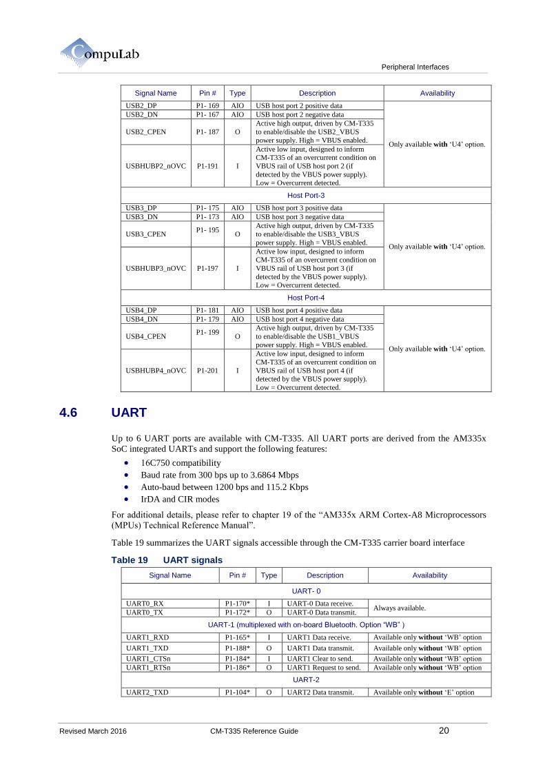
Peripheral Interfaces
Revised March 2016 CM-T335 Reference Guide 20
Signal Name Pin # Type Description Availability
USB2_DP P1- 169 AIO USB host port 2 positive data
Only available with ‘U4’ option.
USB2_DN P1- 167 AIO USB host port 2 negative data
USB2_CPEN P1- 187 O
Active high output, driven by CM-T335
to enable/disable the USB2_VBUS
power supply. High = VBUS enabled.
USBHUBP2_nOVC P1-191 I
Active low input, designed to inform CM-T335 of an overcurrent condition on
VBUS rail of USB host port 2 (if
detected by the VBUS power supply). Low = Overcurrent detected.
Host Port-3
USB3_DP P1- 175 AIO USB host port 3 positive data
Only available with ‘U4’ option.
USB3_DN P1- 173 AIO USB host port 3 negative data
USB3_CPEN P1- 195
O
Active high output, driven by CM-T335
to enable/disable the USB3_VBUS
power supply. High = VBUS enabled.
USBHUBP3_nOVC P1-197 I
Active low input, designed to inform CM-T335 of an overcurrent condition on
VBUS rail of USB host port 3 (if
detected by the VBUS power supply). Low = Overcurrent detected.
Host Port-4
USB4_DP P1- 181 AIO USB host port 4 positive data
Only available with ‘U4’ option.
USB4_DN P1- 179 AIO USB host port 4 negative data
USB4_CPEN P1- 199
O
Active high output, driven by CM-T335
to enable/disable the USB1_VBUS
power supply. High = VBUS enabled.
USBHUBP4_nOVC P1-201 I
Active low input, designed to inform
CM-T335 of an overcurrent condition on
VBUS rail of USB host port 4 (if
detected by the VBUS power supply).
Low = Overcurrent detected.
4.6 UART
Up to 6 UART ports are available with CM-T335. All UART ports are derived from the AM335x
SoC integrated UARTs and support the following features:
16C750 compatibility
Baud rate from 300 bps up to 3.6864 Mbps
Auto-baud between 1200 bps and 115.2 Kbps
IrDA and CIR modes
For additional details, please refer to chapter 19 of the “AM335x ARM Cortex-A8 Microprocessors
(MPUs) Technical Reference Manual”.
Table 19 summarizes the UART signals accessible through the CM-T335 carrier board interface
Table 19 UART signals
Signal Name Pin # Type Description Availability
UART- 0
UART0_RX P1-170* I UART-0 Data receive. Always available.
UART0_TX P1-172* O UART-0 Data transmit.
UART-1 (multiplexed with on-board Bluetooth. Option “WB” )
UART1_RXD P1-165* I UART1 Data receive. Available only without ‘WB’ option
UART1_TXD P1-188* O UART1 Data transmit. Available only without ‘WB’ option
UART1_CTSn P1-184* I UART1 Clear to send. Available only without ‘WB’ option
UART1_RTSn P1-186* O UART1 Request to send. Available only without ‘WB’ option
UART-2
UART2_TXD P1-104* O UART2 Data transmit. Available only without ‘E’ option

Peripheral Interfaces
Revised March 2016 CM-T335 Reference Guide 21
Signal Name Pin # Type Description Availability
UART2_RXD P1-113* I UART2 Data receive. Available only without ‘E’ option
UART-3
UART3_TXD P1-107* O UART3 Data transmit. Available only without ‘E’ option
UART3_RXD P1-109* I UART3 Data receive. Available only without ‘E’ option
UART3_CTSn P1-46* I UART3 Clear to send. Available when display not used
UART3_RTSn P1-39* O UART3 Request to send. Available when display not used
UART-4
UART4_TXD P1-107*
O UART4 Data transmit. Available only without ‘E’ option
P1-139* Available when I2C-1 not used
UART4_RXD P1-109*
I UART4 Data receive. Available only without ‘E’ option
P1-138* Available when I2C-1 not used
UART4_CTSn P1-48* I UART4 Clear to send. Available when display not used
UART4_RTSn P1-43* O UART4 Request to send. Available when display not used
UART-5
UART5_TXD
P1-52*
O UART5 Data transmit.
Available when display not used
P1-125* Available only without ‘E’ option
P1-157* Available only without ‘A’ option
UART5_RXD
P1-50*
I UART5 Data receive.
Available when display not used
P1-41* Available when display not used
P1-141* Available only without ‘A’ option
UART5_CTSn P1-41* I UART4 Clear to send. Available when display not used
UART5_RTSn P1-26* O UART4 Request to send. Available when display not used
Note: Pins denoted with "*" are multifunctional. For details, please refer to section 5.5 of this
document.
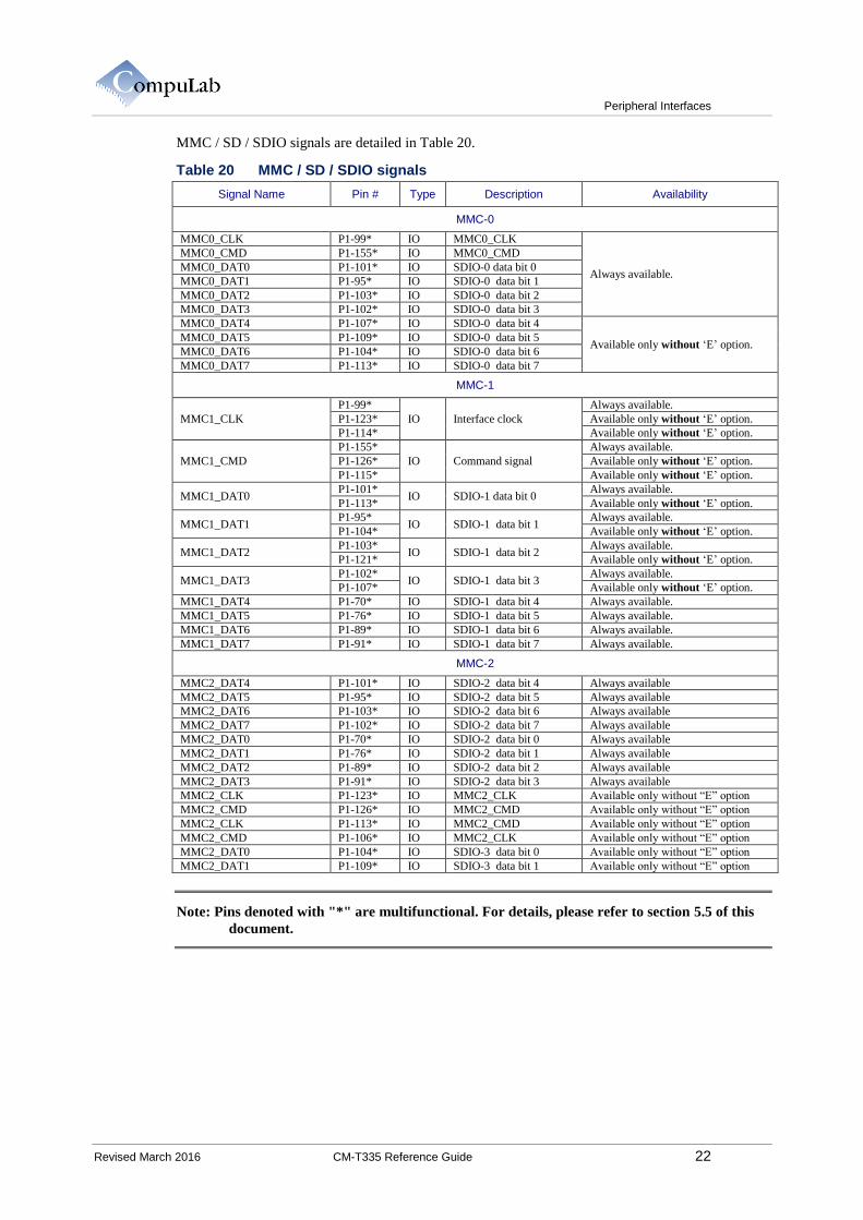
4.7 MMC / SD / SDIO
The CM-T335 features up-to three multimedia card high-speed/secure data/secure digital IO (MMC /
SD / SDIO) host interfaces. Each MMC/SD/SDIO host controller supports a single MMC / SD /
SDIO card or device.
The general features of the MMCHS host controller IP are:
Built-in 1024-byte buffer for read or write
MMC command/response sets as defined in the MMC standard specification v4.3
SD command/response sets as defined in the SD Physical Layer specification v2.00
SDIO command/response sets and interrupt/read-wait suspend-resume operations as defined
in the SD part E1 specification v 2.00
Clock support:
96-MHz functional clock source input
Up to 384Mbit/sec (48MByte/sec) in MMC mode 8-bit data transfer
Up to 192Mbit/sec (24MByte/sec) in High-Speed SD mode 4-bit data transfer
Up to 24Mbit/sec (3MByte/sec) in Default SD mode 1-bit data transfer
For additional details, please refer to chapter 18 of the “AM335x ARM Cortex-A8 Microprocessors
(MPUs) Technical Reference Manual”.
Peripheral Interfaces
Revised March 2016 CM-T335 Reference Guide 22
MMC / SD / SDIO signals are detailed in Table 20.
Table 20 MMC / SD / SDIO signals
Signal Name Pin # Type Description Availability
MMC-0
MMC0_CLK P1-99* IO MMC0_CLK
Always available.
MMC0_CMD P1-155* IO MMC0_CMD
MMC0_DAT0 P1-101* IO SDIO-0 data bit 0
MMC0_DAT1 P1-95* IO SDIO-0 data bit 1
MMC0_DAT2 P1-103* IO SDIO-0 data bit 2
MMC0_DAT3 P1-102* IO SDIO-0 data bit 3
MMC0_DAT4 P1-107* IO SDIO-0 data bit 4
Available only without ‘E’ option. MMC0_DAT5 P1-109* IO SDIO-0 data bit 5
MMC0_DAT6 P1-104* IO SDIO-0 data bit 6
MMC0_DAT7 P1-113* IO SDIO-0 data bit 7
MMC-1
MMC1_CLK
P1-99*
IO Interface clock
Always available.
P1-123* Available only without ‘E’ option.
P1-114* Available only without ‘E’ option.
MMC1_CMD
P1-155*
IO Command signal
Always available.
P1-126* Available only without ‘E’ option.
P1-115* Available only without ‘E’ option.
MMC1_DAT0 P1-101*
IO SDIO-1 data bit 0 Always available.
P1-113* Available only without ‘E’ option.
MMC1_DAT1 P1-95*
IO SDIO-1 data bit 1 Always available.
P1-104* Available only without ‘E’ option.
MMC1_DAT2 P1-103*
IO SDIO-1 data bit 2 Always available.
P1-121* Available only without ‘E’ option.
MMC1_DAT3 P1-102*
IO SDIO-1 data bit 3 Always available.
P1-107* Available only without ‘E’ option.
MMC1_DAT4 P1-70* IO SDIO-1 data bit 4 Always available.
MMC1_DAT5 P1-76* IO SDIO-1 data bit 5 Always available.
MMC1_DAT6 P1-89* IO SDIO-1 data bit 6 Always available.
MMC1_DAT7 P1-91* IO SDIO-1 data bit 7 Always available.
MMC-2
MMC2_DAT4 P1-101* IO SDIO-2 data bit 4 Always available
MMC2_DAT5 P1-95* IO SDIO-2 data bit 5 Always available
MMC2_DAT6 P1-103* IO SDIO-2 data bit 6 Always available
MMC2_DAT7 P1-102* IO SDIO-2 data bit 7 Always available
MMC2_DAT0 P1-70* IO SDIO-2 data bit 0 Always available
MMC2_DAT1 P1-76* IO SDIO-2 data bit 1 Always available
MMC2_DAT2 P1-89* IO SDIO-2 data bit 2 Always available
MMC2_DAT3 P1-91* IO SDIO-2 data bit 3 Always available
MMC2_CLK P1-123* IO MMC2_CLK Available only without “E” option
MMC2_CMD P1-126* IO MMC2_CMD Available only without “E” option
MMC2_CLK P1-113* IO MMC2_CMD Available only without “E” option
MMC2_CMD P1-106* IO MMC2_CLK Available only without “E” option
MMC2_DAT0 P1-104* IO SDIO-3 data bit 0 Available only without “E” option
MMC2_DAT1 P1-109* IO SDIO-3 data bit 1 Available only without “E” option
Note: Pins denoted with "*" are multifunctional. For details, please refer to section 5.5 of this
document.

Peripheral Interfaces
Revised March 2016 CM-T335 Reference Guide 23
4.8 ADC / Touch-Screen
CM-T335 features an ADC module that can act as a resistive touch-screen controller. The interface
supports 4/5/8-wire touch panels and is available through the CM-T335 carrier board interface.
The ADC and touch screen signals are detailed in Table 21.
Table 21 ADC and Touch-Screen Signals
Signal Name Pin # Type Description Availability
AIN0 P1-10 AIO Touch screen X- (left)\ ADC in Always available
AIN1 P1-20 AIO Touch screen X+ (right)\ ADC in Always available
AIN2 P1-6 AIO Touch screen Y+ (top)\ ADC in Always available
AIN3 P1-14 AIO Touch screen Y- (bottom)\ ADC in Always available
AIN4 P1-12 AIO ADC in Always available
AIN5 P1-11 AI ADC in Always available
AIN6 P1-18 AI ADC in Always available
AIN7 P1-16 AI ADC in Always available
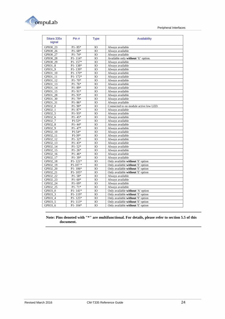
4.9 GPIO
The AM335 provides up to 94 GPIO signals. The GPIO subsystem is derived from the AM335
integrated GPIO controller. The AM335 GPIOs are divided into 4 blocks with up to 31 GPIOs in each
block. The GPIO signals can be configured for the following applications:
Data input / output
Synchronous interrupt generation
Keyboard interface with a de-bouncing cell
GPIO0 block can generate a Wake-up request in Idle mode
For additional details, please refer to section 25 of the “AM335 Reference Manual”.
Note: Not all GPIO signals supported by the AM335x SoC are available through the CM-T335
carrier board interface.
The GPIO signals available through CM-T335 interface are detailed in Table 22.
Table 22 GPIO Signals
Sitara 335x signal
Pin # Type Availability
GPIO0_0 P1-126* IO Only available without 'E' option
GPIO0_1 P1-123* IO Only available without 'E' option
GPIO0_2 P1-200* IO Only available without 'WB' option
GPIO0_3 P1-198* IO Only available without 'WB' option
GPIO0_4 P1-174 * IO Only available without 'WB' option
GPIO0_5 P1-176 * IO Always available
GPIO0_6 P1-182* IO Only available without 'WB' option
GPIO0_7 P1-96 * IO Always available
GPIO0_8 P1- 48* IO Always available
GPIO0_9 P1- 43 * IO Always available
GPIO0_10 P1- 41* IO Always available
GPIO0_11 P1- 26* IO Always available
GPIO0_12 P1- 184* IO Only available without 'WB' option
GPIO0_13 P1- 186* IO Only available without 'WB' option
GPIO0_14 P1- 165* IO Only available without 'WB' option
GPIO0_15 P1-188* IO Only available without 'WB' option
GPIO0_16 P1- 109* IO Only available without 'E' option
GPIO0_17 P1- 117* IO Only available without 'E' option
GPIO0_18 P1-202 * IO Only available without 'U1' option
GPIO0_21 P1-115 * IO Only available without 'E' option
GPIO0_22 P1- 83* IO Always available
Peripheral Interfaces
Revised March 2016 CM-T335 Reference Guide 24
Sitara 335x signal
Pin # Type Availability
GPIO0_23 P1- 85* IO Always available
GPIO0_26 P1- 68* IO Always available
GPIO0_27 P1- 74* IO Always available
GPIO0_28 P1- 114* IO Available only without ‘E’ option.
GPIO0_29 P1- 157* IO Always available
GPIO1_8 P1- 138* IO Always available
GPIO1_9 P1- 139* IO Always available
GPIO1_10 P1- 170* IO Always available
GPIO1_11 P1- 172* IO Always available
GPIO1_12 P1- 70* IO Always available
GPIO1_13 P1- 76* IO Always available
GPIO1_14 P1- 89* IO Always available
GPIO1_15 P1- 91* IO Always available
GPIO1_28 P1- 93* IO Always available
GPIO1_30 P1- 79* IO Always available
GPIO1_31 P1- 86* IO Always available
GPIO2_0 P1- 90* IO Connected to on module active low LED.
GPIO2_1 P1- 87* IO Always available
GPIO2_5 P1- 93* IO Always available
GPIO2_6 P1- 45* IO Always available
GPIO2_7 P1-53* IO Always available
GPIO2_8 P1- 44* IO Always available
GPIO2_9 P1- 47* IO Always available
GPIO2_10 P1-54* IO Always available
GPIO2_11 P1-39* IO Always available
GPIO2_12 P1- 32* IO Always available
GPIO2_13 P1- 43* IO Always available
GPIO2_14 P1- 52* IO Always available
GPIO2_15 P1- 26* IO Always available
GPIO2_16 P1- 46* IO Always available
GPIO2_17 P1- 39* IO Always available
GPIO2_18 P1- 121* IO Only available without 'E' option
GPIO2_19 P1-107 * IO Only available without 'E' option
GPIO2_20 P1- 106* IO Only available without 'E' option
GPIO2_21 P1- 105* IO Only available without 'E' option
GPIO2_22 P1- 58* IO Always available
GPIO2_23 P1- 60* IO Always available
GPIO2_24 P1- 69* IO Always available
GPIO2_25 P1- 71* IO Always available
GPIO3_0 P1- 141* IO Only available without 'A' option
GPIO3_3 P1- 119* IO Only available without 'E' option
GPIO3_4 P1- 125* IO Only available without 'E' option
GPIO3_5 P1- 113* IO Only available without 'E' option
GPIO3_6 P1- 104* IO Only available without 'E' option
Note: Pins denoted with "*" are multifunctional. For details, please refer to section 5.5 of this
document.
Peripheral Interfaces
Revised March 2016 CM-T335 Reference Guide 25
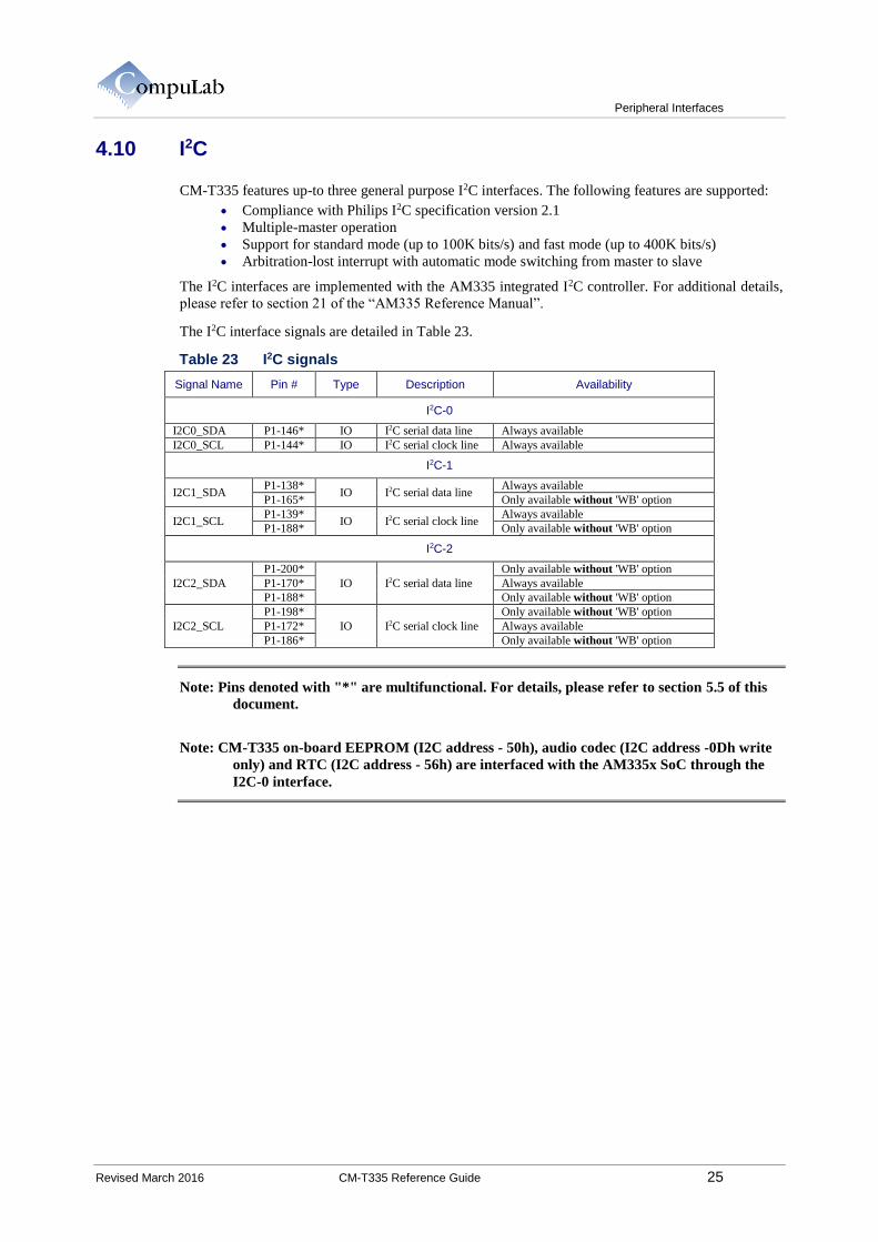
4.10 I2C
CM-T335 features up-to three general purpose I2C interfaces. The following features are supported:
Compliance with Philips I2C specification version 2.1
Multiple-master operation
Support for standard mode (up to 100K bits/s) and fast mode (up to 400K bits/s)
Arbitration-lost interrupt with automatic mode switching from master to slave
The I2C interfaces are implemented with the AM335 integrated I2C controller. For additional details,
please refer to section 21 of the “AM335 Reference Manual”.
The I2C interface signals are detailed in Table 23.
Table 23 I2C signals
Signal Name Pin # Type Description Availability
I2C-0
I2C0_SDA P1-146* IO I2C serial data line Always available
I2C0_SCL P1-144* IO I2C serial clock line Always available
I2C-1
I2C1_SDA P1-138*
IO I2C serial data line Always available
P1-165* Only available without 'WB' option
I2C1_SCL P1-139*
IO I2C serial clock line Always available
P1-188* Only available without 'WB' option
I2C-2
I2C2_SDA
P1-200*
IO I2C serial data line
Only available without 'WB' option
P1-170* Always available
P1-188* Only available without 'WB' option
I2C2_SCL
P1-198*
IO I2C serial clock line
Only available without 'WB' option
P1-172* Always available
P1-186* Only available without 'WB' option
Note: Pins denoted with "*" are multifunctional. For details, please refer to section 5.5 of this
document.
Note: CM-T335 on-board EEPROM (I2C address - 50h), audio codec (I2C address -0Dh write
only) and RTC (I2C address - 56h) are interfaced with the AM335x SoC through the
I2C-0 interface.
Peripheral Interfaces
Revised March 2016 CM-T335 Reference Guide 26
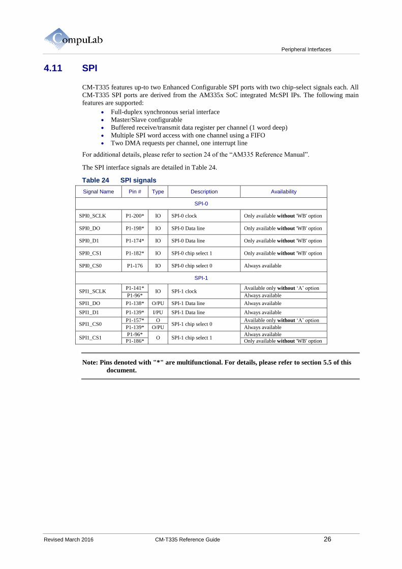
4.11 SPI
CM-T335 features up-to two Enhanced Configurable SPI ports with two chip-select signals each. All
CM-T335 SPI ports are derived from the AM335x SoC integrated McSPI IPs. The following main
features are supported:
Full-duplex synchronous serial interface
Master/Slave configurable
Buffered receive/transmit data register per channel (1 word deep)
Multiple SPI word access with one channel using a FIFO
Two DMA requests per channel, one interrupt line
For additional details, please refer to section 24 of the “AM335 Reference Manual”.
The SPI interface signals are detailed in Table 24.
Table 24 SPI signals
Signal Name Pin # Type Description Availability
SPI-0
SPI0_SCLK P1-200* IO SPI-0 clock Only available without 'WB' option
SPI0_DO P1-198* IO SPI-0 Data line Only available without 'WB' option
SPI0_D1 P1-174* IO SPI-0 Data line Only available without 'WB' option
SPI0_CS1 P1-182* IO SPI-0 chip select 1 Only available without 'WB' option
SPI0_CS0 P1-176 IO SPI-0 chip select 0 Always available
SPI-1
SPI1_SCLK P1-141*
IO SPI-1 clock Available only without ‘A’ option
P1-96* Always available
SPI1_DO P1-138* O/PU SPI-1 Data line Always available
SPI1_D1 P1-139* I/PU SPI-1 Data line Always available
SPI1_CS0 P1-157* O
SPI-1 chip select 0 Available only without ‘A’ option
P1-139* O/PU Always available
SPI1_CS1 P1-96*
O SPI-1 chip select 1 Always available
P1-186* Only available without 'WB' option
Note: Pins denoted with "*" are multifunctional. For details, please refer to section 5.5 of this
document.
Peripheral Interfaces
Revised March 2016 CM-T335 Reference Guide 27
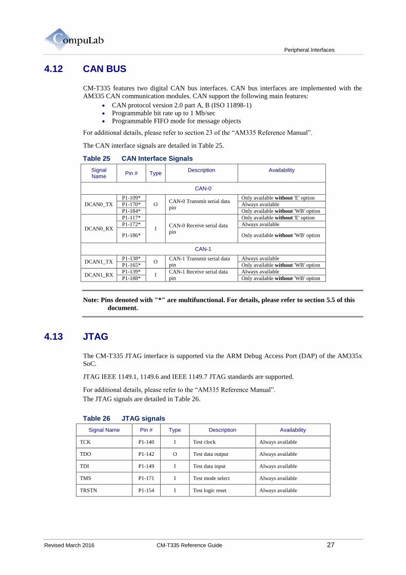
4.12 CAN BUS
CM-T335 features two digital CAN bus interfaces. CAN bus interfaces are implemented with the
AM335 CAN communication modules. CAN support the following main features:
CAN protocol version 2.0 part A, B (ISO 11898-1)
Programmable bit rate up to 1 Mb/sec
Programmable FIFO mode for message objects
For additional details, please refer to section 23 of the “AM335 Reference Manual”.
The CAN interface signals are detailed in Table 25.
Table 25 CAN Interface Signals
Signal Name
Pin # Type Description Availability
CAN-0
DCAN0_TX
P1-109*
O CAN-0 Transmit serial data
pin
Only available without 'E' option
P1-170* Always available
P1-184* Only available without 'WB' option
DCAN0_RX
P1-117*
I CAN-0 Receive serial data
pin
Only available without 'E' option
P1-172* Always available
P1-186* Only available without 'WB' option
CAN-1
DCAN1_TX P1-138*
O CAN-1 Transmit serial data pin
Always available
P1-165* Only available without 'WB' option
DCAN1_RX P1-139*
I CAN-1 Receive serial data
pin
Always available
P1-188* Only available without 'WB' option
Note: Pins denoted with "*" are multifunctional. For details, please refer to section 5.5 of this
document.
4.13 JTAG
The CM-T335 JTAG interface is supported via the ARM Debug Access Port (DAP) of the AM335x
SoC.
JTAG IEEE 1149.1, 1149.6 and IEEE 1149.7 JTAG standards are supported.
For additional details, please refer to the “AM335 Reference Manual”.
The JTAG signals are detailed in Table 26.
Table 26 JTAG signals
Signal Name Pin # Type Description Availability
TCK P1-140 I Test clock Always available
TDO P1-142 O Test data output Always available
TDI P1-149 I Test data input Always available
TMS P1-171 I Test mode select Always available
TRSTN P1-154 I Test logic reset Always available
System Logic
Revised March 2016 CM-T335 Reference Guide 28
5 SYSTEM LOGIC
5.1 Power Management
CM-T335 features a Power Management IC (PMIC) which supports the SoC and the peripheral
power rails. The PMIC integrates step down converters, power fail protection and thermal shutdown
protection.
The power rails that support the CM-T335 are detailed in Table 27.
Table 8 Power Rails Operating Conditions
Supply Name Min Typ. Max Unit Description
VIN 3.0 3.3 3.6 V Main power supply. Converted to multiple power rails by the PMIC
VDD_RTC_BACK 1.4 5.0 5.5 V Backup power supply for RTC
USB0_VBUS 0 5.0 5.25 V USB power supply, regulated by the SoC (see note)
Note: USB0_VBUS voltage supply of more than 4.75 V is required for proper USB operation.
For proper operation of USB, the VBUS must be USB0_DRVVBUS dependent. Refer
to SB-T335 reference design.
For additional details, please refer to the AM335x datasheet, available from Texas Instruments.
5.2 Reset
The reset management of the AM335x SoC is done by the on-chip Power, Reset and Clock
Management (PRCM) module. It can receive reset input from several sources, of two types: warm
reset and cold reset.
For additional details, please refer to section 8.1.7 of the “AM335x ARM Cortex-A8 Microprocessors
(MPUs) Technical Reference Manual”.
Two of the reset sources for the PRCM module are hardware pins that can be addressed externally to
the CM-T335. Both of the reset signals are active low and have on-board pull-up resistors of
10.5KOhm.
The CM-T335 reset signals are detailed in Table 28.
Table 9 Reset signals
Signal Name Pin # Description
nRESET P1-7 Global cold reset (power-on-reset). Should be asserted (low) for at least 1.5 msec.
WARMRST# P1-15 Global warm reset

System Logic
Revised March 2016 CM-T335 Reference Guide 29
5.3 Boot Sequence
On startup, at PWRONRSTN reset signal rising edge, the boot sequence is configured according to
SYSBOOT input terminals. After booting device list creation, the AM335x initiates a booting
procedure. If a boot image is found on a device, the boot code executes. Otherwise, the next boot
device enumerated in the list is examined. The device waits for the watchdog to deliver a reset signal
and restart the boot procedure.
5.3.1 Boot Sequence since CM-T335 rev1.11
CM-T335 rev1.11 and higher are configured for boot sequence as described in Table 28a.
Table 28a Boot Sequence since CM-T335 rev1.11
1st 2nd 3rd 4th
NAND NANI2C SPI0 EMAC1
It is possible to implement boot from MMC0 by alternating the standard boot sequence. It is not
recommended to use MMC0 as the main system boot device, but only as system recovery media. To
perform the alternative boot sequence, LCD_DATA4 line must be pulled down by a 1k resistor
during the start up or cold reset routines.
Table 28b CM-T335 rev1.11 Alternative Boot Sequence
1st 2nd 3rd 4th
UART0 XIP MMC0 NAND
5.3.2 Boot Sequence in CM-T335 rev1.1
CM-T335 rev1.1 is configured for boot sequence as described in Table 28c.
Table 28c Boot Sequence in CM-T335 rev1.11
1st 2nd 3rd 4th
UART0 XIP MMC0 NAND
5.3.3 Additional Boot Configuration Signals
In addition to the boot sequence, additional boot configurations are done on startup, according to
AM335x SYSBOOT terminals.
Additional boot configurations made for CM-T335:
Crystal frequency: 25MHz
Non-muxed XIP
ECC done by ROM
Bus width for XIP boot: 8 bit
CLKOUT1 output enabled
For more information regarding booting, refer to chapter 26.1.5 of the “AM335 Reference Manual”.
Note: LCD_DATA[0:15] lines function as SYSBOOT input at PWRONRSTn rising edge.
Therefore these pins must not be driven by the carrier board during CM-T335x boot
process.
System Logic
Revised March 2016 CM-T335 Reference Guide 30
5.4 RTC
CM-T335 features an on-board ultra-low-power EM3027 real time clock (RTC).
The RTC is connected to the AM335x SoC using I2C 0 interface at address 56h.
At main power supply absence, in order to maintain activities of the RTC, i.e. clock advancement and
data storage, a use of a backup supply is essential. The backup supply may be derived from a super-
cap or a battery. A battery can be charged from the VCC voltage using an internal trickle charger of
the RTC.
For more information about RTC refer to the EM3027 datasheet.
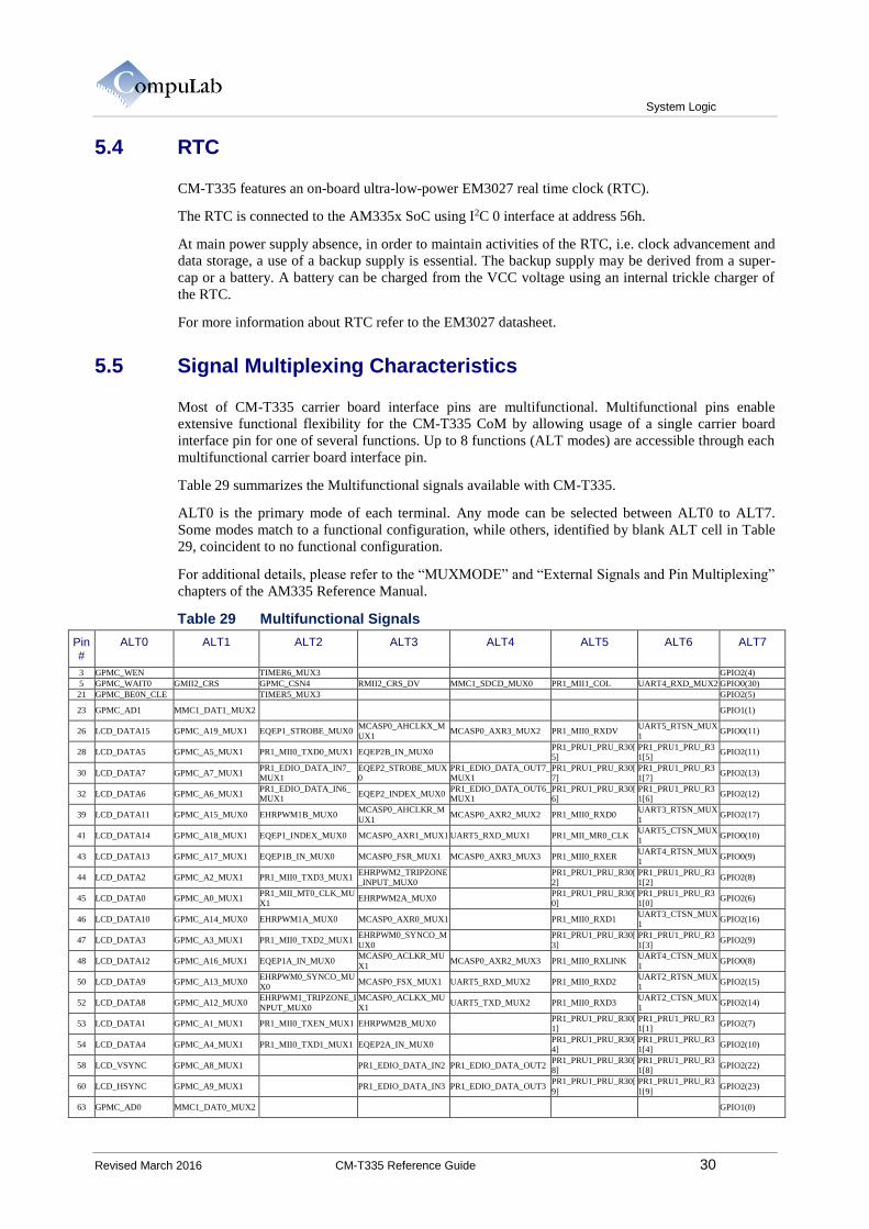
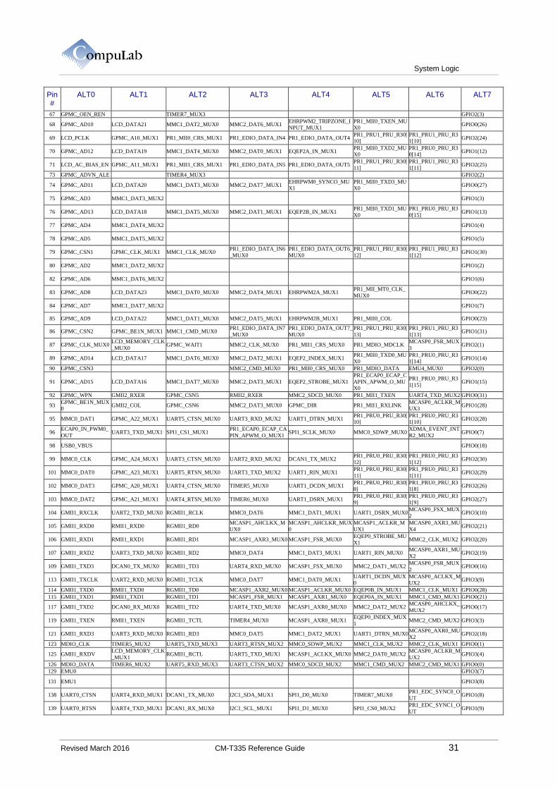
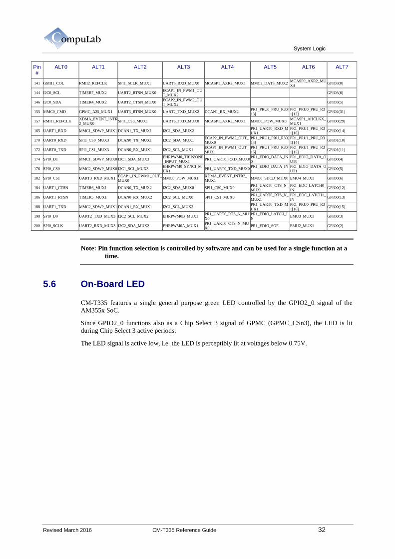
5.5 Signal Multiplexing Characteristics
Most of CM-T335 carrier board interface pins are multifunctional. Multifunctional pins enable
extensive functional flexibility for the CM-T335 CoM by allowing usage of a single carrier board
interface pin for one of several functions. Up to 8 functions (ALT modes) are accessible through each
multifunctional carrier board interface pin.
Table 29 summarizes the Multifunctional signals available with CM-T335.
ALT0 is the primary mode of each terminal. Any mode can be selected between ALT0 to ALT7.
Some modes match to a functional configuration, while others, identified by blank ALT cell in Table
29, coincident to no functional configuration.
For additional details, please refer to the “MUXMODE” and “External Signals and Pin Multiplexing”
chapters of the AM335 Reference Manual.
Table 29 Multifunctional Signals
Pin #
ALT0 ALT1 ALT2 ALT3 ALT4 ALT5 ALT6 ALT7
3 GPMC_WEN TIMER6_MUX3 GPIO2(4)
5 GPMC_WAIT0 GMII2_CRS GPMC_CSN4 RMII2_CRS_DV MMC1_SDCD_MUX0 PR1_MII1_COL UART4_RXD_MUX2 GPIO0(30)
21 GPMC_BE0N_CLE TIMER5_MUX3 GPIO2(5)
23 GPMC_AD1 MMC1_DAT1_MUX2 GPIO1(1)
26 LCD_DATA15 GPMC_A19_MUX1 EQEP1_STROBE_MUX0 MCASP0_AHCLKX_M
UX1 MCASP0_AXR3_MUX2 PR1_MII0_RXDV
UART5_RTSN_MUX
1 GPIO0(11)
28 LCD_DATA5 GPMC_A5_MUX1 PR1_MII0_TXD0_MUX1 EQEP2B_IN_MUX0 PR1_PRU1_PRU_R30[
5]
PR1_PRU1_PRU_R3
1[5] GPIO2(11)
30 LCD_DATA7 GPMC_A7_MUX1 PR1_EDIO_DATA_IN7_
MUX1
EQEP2_STROBE_MUX
0
PR1_EDIO_DATA_OUT7_
MUX1
PR1_PRU1_PRU_R30[
7]
PR1_PRU1_PRU_R3
1[7] GPIO2(13)
32 LCD_DATA6 GPMC_A6_MUX1 PR1_EDIO_DATA_IN6_
MUX1 EQEP2_INDEX_MUX0
PR1_EDIO_DATA_OUT6_
MUX1
PR1_PRU1_PRU_R30[
6]
PR1_PRU1_PRU_R3
1[6] GPIO2(12)
39 LCD_DATA11 GPMC_A15_MUX0 EHRPWM1B_MUX0 MCASP0_AHCLKR_M
UX1 MCASP0_AXR2_MUX2 PR1_MII0_RXD0
UART3_RTSN_MUX
1 GPIO2(17)
41 LCD_DATA14 GPMC_A18_MUX1 EQEP1_INDEX_MUX0 MCASP0_AXR1_MUX1 UART5_RXD_MUX1 PR1_MII_MR0_CLK UART5_CTSN_MUX
1 GPIO0(10)
43 LCD_DATA13 GPMC_A17_MUX1 EQEP1B_IN_MUX0 MCASP0_FSR_MUX1 MCASP0_AXR3_MUX3 PR1_MII0_RXER UART4_RTSN_MUX
1 GPIO0(9)
44 LCD_DATA2 GPMC_A2_MUX1 PR1_MII0_TXD3_MUX1 EHRPWM2_TRIPZONE
_INPUT_MUX0
PR1_PRU1_PRU_R30[
2]
PR1_PRU1_PRU_R3
1[2] GPIO2(8)
45 LCD_DATA0 GPMC_A0_MUX1 PR1_MII_MT0_CLK_MU
X1 EHRPWM2A_MUX0
PR1_PRU1_PRU_R30[
0]
PR1_PRU1_PRU_R3
1[0] GPIO2(6)
46 LCD_DATA10 GPMC_A14_MUX0 EHRPWM1A_MUX0 MCASP0_AXR0_MUX1 PR1_MII0_RXD1 UART3_CTSN_MUX
1 GPIO2(16)
47 LCD_DATA3 GPMC_A3_MUX1 PR1_MII0_TXD2_MUX1 EHRPWM0_SYNCO_M
UX0
PR1_PRU1_PRU_R30[
3]
PR1_PRU1_PRU_R3
1[3] GPIO2(9)
48 LCD_DATA12 GPMC_A16_MUX1 EQEP1A_IN_MUX0 MCASP0_ACLKR_MU
X1 MCASP0_AXR2_MUX3 PR1_MII0_RXLINK
UART4_CTSN_MUX
1 GPIO0(8)
50 LCD_DATA9 GPMC_A13_MUX0 EHRPWM0_SYNCO_MU
X0 MCASP0_FSX_MUX1 UART5_RXD_MUX2 PR1_MII0_RXD2
UART2_RTSN_MUX
1 GPIO2(15)
52 LCD_DATA8 GPMC_A12_MUX0 EHRPWM1_TRIPZONE_I
NPUT_MUX0
MCASP0_ACLKX_MU
X1 UART5_TXD_MUX2 PR1_MII0_RXD3
UART2_CTSN_MUX
1 GPIO2(14)
53 LCD_DATA1 GPMC_A1_MUX1 PR1_MII0_TXEN_MUX1 EHRPWM2B_MUX0 PR1_PRU1_PRU_R30[
1]
PR1_PRU1_PRU_R3
1[1] GPIO2(7)
54 LCD_DATA4 GPMC_A4_MUX1 PR1_MII0_TXD1_MUX1 EQEP2A_IN_MUX0 PR1_PRU1_PRU_R30[
4]
PR1_PRU1_PRU_R3
1[4] GPIO2(10)
58 LCD_VSYNC GPMC_A8_MUX1 PR1_EDIO_DATA_IN2 PR1_EDIO_DATA_OUT2 PR1_PRU1_PRU_R30[
8]
PR1_PRU1_PRU_R3
1[8] GPIO2(22)
60 LCD_HSYNC GPMC_A9_MUX1 PR1_EDIO_DATA_IN3 PR1_EDIO_DATA_OUT3 PR1_PRU1_PRU_R30[
9]
PR1_PRU1_PRU_R3
1[9] GPIO2(23)
63 GPMC_AD0 MMC1_DAT0_MUX2 GPIO1(0)
System Logic
Revised March 2016 CM-T335 Reference Guide 31
Pin #
ALT0 ALT1 ALT2 ALT3 ALT4 ALT5 ALT6 ALT7
67 GPMC_OEN_REN TIMER7_MUX3 GPIO2(3)
68 GPMC_AD10 LCD_DATA21 MMC1_DAT2_MUX0 MMC2_DAT6_MUX1 EHRPWM2_TRIPZONE_I
NPUT_MUX1
PR1_MII0_TXEN_MU
X0 GPIO0(26)
69 LCD_PCLK GPMC_A10_MUX1 PR1_MII0_CRS_MUX1 PR1_EDIO_DATA_IN4 PR1_EDIO_DATA_OUT4 PR1_PRU1_PRU_R30[
10]
PR1_PRU1_PRU_R3
1[10] GPIO2(24)
70 GPMC_AD12 LCD_DATA19 MMC1_DAT4_MUX0 MMC2_DAT0_MUX1 EQEP2A_IN_MUX1 PR1_MII0_TXD2_MU
X0
PR1_PRU0_PRU_R3
0[14] GPIO1(12)
71 LCD_AC_BIAS_EN GPMC_A11_MUX1 PR1_MII1_CRS_MUX1 PR1_EDIO_DATA_IN5 PR1_EDIO_DATA_OUT5 PR1_PRU1_PRU_R30[
11]
PR1_PRU1_PRU_R3
1[11] GPIO2(25)
73 GPMC_ADVN_ALE TIMER4_MUX3 GPIO2(2)
74 GPMC_AD11 LCD_DATA20 MMC1_DAT3_MUX0 MMC2_DAT7_MUX1 EHRPWM0_SYNCO_MU
X1
PR1_MII0_TXD3_MU
X0 GPIO0(27)
75 GPMC_AD3 MMC1_DAT3_MUX2 GPIO1(3)
76 GPMC_AD13 LCD_DATA18 MMC1_DAT5_MUX0 MMC2_DAT1_MUX1 EQEP2B_IN_MUX1 PR1_MII0_TXD1_MU
X0
PR1_PRU0_PRU_R3
0[15] GPIO1(13)
77 GPMC_AD4 MMC1_DAT4_MUX2 GPIO1(4)
78 GPMC_AD5 MMC1_DAT5_MUX2 GPIO1(5)
79 GPMC_CSN1 GPMC_CLK_MUX1 MMC1_CLK_MUX0 PR1_EDIO_DATA_IN6
_MUX0
PR1_EDIO_DATA_OUT6_
MUX0
PR1_PRU1_PRU_R30[
12]
PR1_PRU1_PRU_R3
1[12] GPIO1(30)
80 GPMC_AD2 MMC1_DAT2_MUX2 GPIO1(2)
82 GPMC_AD6 MMC1_DAT6_MUX2 GPIO1(6)
83 GPMC_AD8 LCD_DATA23 MMC1_DAT0_MUX0 MMC2_DAT4_MUX1 EHRPWM2A_MUX1 PR1_MII_MT0_CLK_
MUX0 GPIO0(22)
84 GPMC_AD7 MMC1_DAT7_MUX2 GPIO1(7)
85 GPMC_AD9 LCD_DATA22 MMC1_DAT1_MUX0 MMC2_DAT5_MUX1 EHRPWM2B_MUX1 PR1_MII0_COL GPIO0(23)
86 GPMC_CSN2 GPMC_BE1N_MUX1 MMC1_CMD_MUX0 PR1_EDIO_DATA_IN7
_MUX0
PR1_EDIO_DATA_OUT7_
MUX0
PR1_PRU1_PRU_R30[
13]
PR1_PRU1_PRU_R3
1[13] GPIO1(31)
87 GPMC_CLK_MUX0 LCD_MEMORY_CLK
_MUX0 GPMC_WAIT1 MMC2_CLK_MUX0 PR1_MII1_CRS_MUX0 PR1_MDIO_MDCLK
MCASP0_FSR_MUX
3 GPIO2(1)
89 GPMC_AD14 LCD_DATA17 MMC1_DAT6_MUX0 MMC2_DAT2_MUX1 EQEP2_INDEX_MUX1 PR1_MII0_TXD0_MU
X0
PR1_PRU0_PRU_R3
1[14] GPIO1(14)
90 GPMC_CSN3 MMC2_CMD_MUX0 PR1_MII0_CRS_MUX0 PR1_MDIO_DATA EMU4_MUX0 GPIO2(0)
91 GPMC_AD15 LCD_DATA16 MMC1_DAT7_MUX0 MMC2_DAT3_MUX1 EQEP2_STROBE_MUX1
PR1_ECAP0_ECAP_C
APIN_APWM_O_MU
X0
PR1_PRU0_PRU_R3
1[15] GPIO1(15)
92 GPMC_WPN GMII2_RXER GPMC_CSN5 RMII2_RXER MMC2_SDCD_MUX0 PR1_MII1_TXEN UART4_TXD_MUX2 GPIO0(31)
93 GPMC_BE1N_MUX
0 GMII2_COL GPMC_CSN6 MMC2_DAT3_MUX0 GPMC_DIR PR1_MII1_RXLINK
MCASP0_ACLKR_M
UX3 GPIO1(28)
95 MMC0_DAT1 GPMC_A22_MUX1 UART5_CTSN_MUX0 UART3_RXD_MUX2 UART1_DTRN_MUX1 PR1_PRU0_PRU_R30[
10]
PR1_PRU0_PRU_R3
1[10] GPIO2(28)
96 ECAP0_IN_PWM0_
OUT UART3_TXD_MUX1 SPI1_CS1_MUX1
PR1_ECAP0_ECAP_CA
PIN_APWM_O_MUX1 SPI1_SCLK_MUX0 MMC0_SDWP_MUX0
XDMA_EVENT_INT
R2_MUX2 GPIO0(7)
98 USB0_VBUS GPIO0(18)
99 MMC0_CLK GPMC_A24_MUX1 UART3_CTSN_MUX0 UART2_RXD_MUX2 DCAN1_TX_MUX2 PR1_PRU0_PRU_R30[
12]
PR1_PRU0_PRU_R3
1[12] GPIO2(30)
101 MMC0_DAT0 GPMC_A23_MUX1 UART5_RTSN_MUX0 UART3_TXD_MUX2 UART1_RIN_MUX1 PR1_PRU0_PRU_R30[
11]
PR1_PRU0_PRU_R3
1[11] GPIO2(29)
102 MMC0_DAT3 GPMC_A20_MUX1 UART4_CTSN_MUX0 TIMER5_MUX0 UART1_DCDN_MUX1 PR1_PRU0_PRU_R30[
8]
PR1_PRU0_PRU_R3
1[8] GPIO2(26)
103 MMC0_DAT2 GPMC_A21_MUX1 UART4_RTSN_MUX0 TIMER6_MUX0 UART1_DSRN_MUX1 PR1_PRU0_PRU_R30[
9]
PR1_PRU0_PRU_R3
1[9] GPIO2(27)
104 GMII1_RXCLK UART2_TXD_MUX0 RGMII1_RCLK MMC0_DAT6 MMC1_DAT1_MUX1 UART1_DSRN_MUX0 MCASP0_FSX_MUX
2 GPIO3(10)
105 GMII1_RXD0 RMII1_RXD0 RGMII1_RD0 MCASP1_AHCLKX_M
UX0
MCASP1_AHCLKR_MUX
0
MCASP1_ACLKR_M
UX1
MCASP0_AXR3_MU
X4 GPIO2(21)
106 GMII1_RXD1 RMII1_RXD1 RGMII1_RD1 MCASP1_AXR3_MUX0 MCASP1_FSR_MUX0 EQEP0_STROBE_MU
X1 MMC2_CLK_MUX2 GPIO2(20)
107 GMII1_RXD2 UART3_TXD_MUX0 RGMII1_RD2 MMC0_DAT4 MMC1_DAT3_MUX1 UART1_RIN_MUX0 MCASP0_AXR1_MU
X2 GPIO2(19)
109 GMII1_TXD3 DCAN0_TX_MUX0 RGMII1_TD3 UART4_RXD_MUX0 MCASP1_FSX_MUX0 MMC2_DAT1_MUX2 MCASP0_FSR_MUX
2 GPIO0(16)
113 GMII1_TXCLK UART2_RXD_MUX0 RGMII1_TCLK MMC0_DAT7 MMC1_DAT0_MUX1 UART1_DCDN_MUX
0
MCASP0_ACLKX_M
UX2 GPIO3(9)
114 GMII1_TXD0 RMII1_TXD0 RGMII1_TD0 MCASP1_AXR2_MUX0 MCASP1_ACLKR_MUX0 EQEP0B_IN_MUX1 MMC1_CLK_MUX1 GPIO0(28)
115 GMII1_TXD1 RMII1_TXD1 RGMII1_TD1 MCASP1_FSR_MUX1 MCASP1_AXR1_MUX0 EQEP0A_IN_MUX1 MMC1_CMD_MUX1 GPIO0(21)
117 GMII1_TXD2 DCAN0_RX_MUX0 RGMII1_TD2 UART4_TXD_MUX0 MCASP1_AXR0_MUX0 MMC2_DAT2_MUX2 MCASP0_AHCLKX_
MUX2 GPIO0(17)
119 GMII1_TXEN RMII1_TXEN RGMII1_TCTL TIMER4_MUX0 MCASP1_AXR0_MUX1 EQEP0_INDEX_MUX
1 MMC2_CMD_MUX2 GPIO3(3)
121 GMII1_RXD3 UART3_RXD_MUX0 RGMII1_RD3 MMC0_DAT5 MMC1_DAT2_MUX1 UART1_DTRN_MUX0 MCASP0_AXR0_MU
X2 GPIO2(18)
123 MDIO_CLK TIMER5_MUX2 UART5_TXD_MUX3 UART3_RTSN_MUX2 MMC0_SDWP_MUX2 MMC1_CLK_MUX2 MMC2_CLK_MUX1 GPIO0(1)
125 GMII1_RXDV LCD_MEMORY_CLK
_MUX1 RGMII1_RCTL UART5_TXD_MUX1 MCASP1_ACLKX_MUX0 MMC2_DAT0_MUX2
MCASP0_ACLKR_M
UX2 GPIO3(4)
126 MDIO_DATA TIMER6_MUX2 UART5_RXD_MUX3 UART3_CTSN_MUX2 MMC0_SDCD_MUX2 MMC1_CMD_MUX2 MMC2_CMD_MUX1 GPIO0(0)
129 EMU0 GPIO3(7)
131 EMU1 GPIO3(8)
138 UART0_CTSN UART4_RXD_MUX1 DCAN1_TX_MUX0 I2C1_SDA_MUX1 SPI1_D0_MUX0 TIMER7_MUX0 PR1_EDC_SYNC0_O
UT GPIO1(8)
139 UART0_RTSN UART4_TXD_MUX1 DCAN1_RX_MUX0 I2C1_SCL_MUX1 SPI1_D1_MUX0 SPI1_CS0_MUX2 PR1_EDC_SYNC1_O
UT GPIO1(9)
System Logic
Revised March 2016 CM-T335 Reference Guide 32
Pin #
ALT0 ALT1 ALT2 ALT3 ALT4 ALT5 ALT6 ALT7
141 GMII1_COL RMII2_REFCLK SPI1_SCLK_MUX1 UART5_RXD_MUX0 MCASP1_AXR2_MUX1 MMC2_DAT3_MUX2 MCASP0_AXR2_MU
X4 GPIO3(0)
144 I2C0_SCL TIMER7_MUX2 UART2_RTSN_MUX0 ECAP1_IN_PWM1_OU
T_MUX2 GPIO3(6)
146 I2C0_SDA TIMER4_MUX2 UART2_CTSN_MUX0 ECAP2_IN_PWM2_OU
T_MUX2 GPIO3(5)
155 MMC0_CMD GPMC_A25_MUX1 UART3_RTSN_MUX0 UART2_TXD_MUX2 DCAN1_RX_MUX2 PR1_PRU0_PRU_R30[
13]
PR1_PRU0_PRU_R3
1[13] GPIO2(31)
157 RMII1_REFCLK XDMA_EVENT_INTR
2_MUX0 SPI1_CS0_MUX1 UART5_TXD_MUX0 MCASP1_AXR3_MUX1 MMC0_POW_MUX0
MCASP1_AHCLKX_
MUX1 GPIO0(29)
165 UART1_RXD MMC1_SDWP_MUX1 DCAN1_TX_MUX1 I2C1_SDA_MUX2 PR1_UART0_RXD_M
UX1
PR1_PRU1_PRU_R3
1[16] GPIO0(14)
170 UART0_RXD SPI1_CS0_MUX3 DCAN0_TX_MUX1 I2C2_SDA_MUX1 ECAP2_IN_PWM2_OUT_
MUX0
PR1_PRU1_PRU_R30[
14]
PR1_PRU1_PRU_R3
1[14] GPIO1(10)
172 UART0_TXD SPI1_CS1_MUX3 DCAN0_RX_MUX1 I2C2_SCL_MUX1 ECAP1_IN_PWM1_OUT_
MUX1
PR1_PRU1_PRU_R30[
15]
PR1_PRU1_PRU_R3
1[15] GPIO1(11)
174 SPI0_D1 MMC1_SDWP_MUX0 I2C1_SDA_MUX3 EHRPWM0_TRIPZONE
_INPUT_MUX1 PR1_UART0_RXD_MUX0
PR1_EDIO_DATA_IN
0
PR1_EDIO_DATA_O
UT0 GPIO0(4)
176 SPI0_CS0 MMC2_SDWP_MUX0 I2C1_SCL_MUX3 EHRPWM0_SYNCI_M
UX1 PR1_UART0_TXD_MUX0
PR1_EDIO_DATA_IN
1
PR1_EDIO_DATA_O
UT1 GPIO0(5)
182 SPI0_CS1 UART3_RXD_MUX1 ECAP1_IN_PWM1_OUT_
MUX0 MMC0_POW_MUX1
XDMA_EVENT_INTR2_
MUX1 MMC0_SDCD_MUX0 EMU4_MUX1 GPIO0(6)
184 UART1_CTSN TIMER6_MUX1 DCAN0_TX_MUX2 I2C2_SDA_MUX0 SPI1_CS0_MUX0 PR1_UART0_CTS_N_
MUX1
PR1_EDC_LATCH0_
IN GPIO0(12)
186 UART1_RTSN TIMER5_MUX1 DCAN0_RX_MUX2 I2C2_SCL_MUX0 SPI1_CS1_MUX0 PR1_UART0_RTS_N_
MUX1
PR1_EDC_LATCH1_
IN GPIO0(13)
188 UART1_TXD MMC2_SDWP_MUX1 DCAN1_RX_MUX1 I2C1_SCL_MUX2 PR1_UART0_TXD_M
UX1
PR1_PRU0_PRU_R3
1[16] GPIO0(15)
198 SPI0_D0 UART2_TXD_MUX3 I2C2_SCL_MUX2 EHRPWM0B_MUX1 PR1_UART0_RTS_N_MU
X0
PR1_EDIO_LATCH_I
N EMU3_MUX1 GPIO0(3)
200 SPI0_SCLK UART2_RXD_MUX3 I2C2_SDA_MUX2 EHRPWM0A_MUX1 PR1_UART0_CTS_N_MU
X0 PR1_EDIO_SOF EMU2_MUX1 GPIO0(2)
Note: Pin function selection is controlled by software and can be used for a single function at a
time.
5.6 On-Board LED
CM-T335 features a single general purpose green LED controlled by the GPIO2_0 signal of the
AM355x SoC.
Since GPIO2_0 functions also as a Chip Select 3 signal of GPMC (GPMC_CSn3), the LED is lit
during Chip Select 3 active periods.
The LED signal is active low, i.e. the LED is perceptibly lit at voltages below 0.75V.

Carrier board Interface
Revised March 2016 CM-T335 Reference Guide 33
6 CARRIER BOARD INTERFACE
CM-T335 connects to the carrier board through a standard 204-pin SODIMM edge connector.
The pinout is specified in table 30.
6.1 Connector Pinout
Table 30 Connector Pinout
Pin #
CM-T335 Signal Name AM335x Signal Name Type Description Reference Section
1 VIN PWR Main power supply, 3.3V typ. 5.1
2 NC Not connected -
3 GPMC_WE# GPMC_WEn O GPMC Write Enable (active low) -
4 NC Not connected -
5 GPMC_WAIT0 GPMC_WAIT0 I External wait signal for access time control (pulled up) 4.7
6 AIN2 AIN2 AIO General purpose analog input/output / touch screen input 4.8
7 nRESET RTC_PWRONRSTN I Global cold reset (active low) 5.2
8 VIN PWR Main power supply, 3.3V typ. 5.1
9 NC Not connected -
10 AIN0 AIN0 AIO General purpose analog input/output / touch screen input 4.8
11 AIN5 AIN5 AI General purpose analog input / touch screen input 4.8
12 AIN4 AIN4 AIO General purpose analog input/output / touch screen input 4.8
13 NC Not connected -
14 AIN3 AIN3 AIO General purpose analog input/output / touch screen input 4.8
15 WARMRST# nRESETIN_OUT I Global warm reset (active low) 5.2
16 AIN7 AIN7 AI General purpose analog input / touch screen input 4.8
17 GND Digital ground -
18 AIN6 AIN6 AI General purpose analog input / touch screen input 4.8
19 NC Not connected -
20 AIN1 AIN1 AIO General purpose analog input/output / touch screen input 4.8
21 GPMC_CLE GPMC_BE0n_CLE O Command Line Enable for NAND protocol -
22 NC Not connected -
23 GPMC_AD1 GPMC_AD1 IO GPMC DATA 1 4.7
24 GND Digital ground -
25 NC Not connected -
26 LCD_DATA15 LCD_DATA15 O LCD data bus 4.1, 4.6
27 NC Not connected -
28 LCD_DATA5 LCD_DATA5 O LCD data bus 4.1
29 NC Not connected -
30 LCD_DATA7 LCD_DATA7 O LCD data bus 4.1
31 NC Not connected -
32 LCD_DATA6 LCD_DATA6 O LCD data bus 4.1
33 VIN PWR Main power supply, 3.3V typ. 5.1
34 NC Not connected -
35 NC Not connected -
36 NC Not connected -
37 NC Not connected -
38 NC Not connected -
39 LCD_DATA11 LCD_DATA11 O LCD data bus 4.1, 4.6
40 VIN Main power supply, 3.3V typ. 5.1
41 LCD_DATA14 LCD_DATA14 O LCD data bus 4.1, 4.6
42 NC Not connected -
43 LCD_DATA13 LCD_DATA13 O LCD data bus 4.1, 4.6
44 LCD_DATA2 LCD_DATA2 O LCD data bus 4.1
45 LCD_DATA0 LCD_DATA0 O LCD data bus 4.1
46 LCD_DATA10 LCD_DATA10 O LCD data bus 4.1, 4.6
47 LCD_DATA3 LCD_DATA3 O LCD data bus 4.1
48 LCD_DATA12 LCD_DATA12 O LCD data bus 4.1, 4.6
49 GND Digital ground -
50 LCD_DATA9 LCD_DATA9 O LCD data bus 4.1, 4.6
51 NC Not connected -
52 LCD_DATA8 LCD_DATA8 O LCD data bus 4.1, 4.6

Carrier board Interface
Revised March 2016 CM-T335 Reference Guide 34
53 LCD_DATA1 LCD_DATA1 O LCD data bus 4.1
54 LCD_DATA4 LCD_DATA4 O LCD data bus 4.1
55 NC Not connected -
56 GND Digital ground -
57 NC Not connected -
58 LCD_VSYNC LCD_VSYNC O LCD Vertical Sync 4.1
59 EXT_WAKEUP EXT_WAKEUP I External wake-up input
60 LCD_HSYNC LCD_HSYNC O LCD Horizontal Sync 4.1
61 NC Not connected -
62 NC Not connected -
63 GPMC_AD0 GPMC_AD0 IO GPMC DATA 0 4.7
64 NC Not connected -
65 VIN PWR Main power supply, 3.3V typ. 5.1
66 NC Not connected -
67 GPMC_RE# GPMC_OEn_REn O GPMC Read Enable (active low) -
68 LCD_DATA21 LCD_DATA21 O LCD data bus 4.1, 4.7
69 LCD_PCLK LCD_PCLK O LCD Pixel Clock 4.1
70 LCD_DATA19 LCD_DATA19 O LCD data bus 4.1, 4.7
71 LCD_BIAS_EN LCD_AC_BIAS_EN O LCD AC bias enable chip select 4.1
72 VIN PWR Main power supply, 3.3V typ. 5.1
73 GPMC_ALE GPMC_ADVn_ALE O Address Latch Enable for NAND or NOR protocol -
74 LCD_DATA20 LCD_DATA20 O LCD data bus 4.1, 4.7
75 GPMC_AD3 GPMC_AD3 IO GPMC DATA 3 4.7
76 LCD_DATA18 LCD_DATA18 O LCD data bus 4.1, 4.7
77 GPMC_AD4 GPMC_AD4 IO GPMC DATA 4 4.7
78 GPMC_AD5 GPMC_AD5 IO GPMC DATA 5 4.7
79 GPMC_CS1 GPMC_CSn1 O GPMC Chip Select 1 (active low) 4.7
80 GPMC_AD2 IO GPMC DATA 2 4.7
81 GND Digital ground -
82 GPMC_AD6 GPMC_AD6 IO GPMC DATA 6 4.7
83 LCD_DATA23 LCD_DATA23 O LCD data bus 4.1
84 GPMC_AD7 GPMC_AD7 IO GPMC DATA 7 4.7
85 LCD_DATA22 LCD_DATA22 O LCD data bus 4.1
86 GPMC_CS2 GPMC_CSn2 O GPMC Chip Select 2 (active low) 4.7
87 GPMC_CLK GPMC_CLK O GPMC synchronous mode clock 4.7
88 GND Digital ground -
89 LCD_DATA17 LCD_DATA17 O LCD data bus 4.1, 4.7
90 GPMCCS3_GPIO2_0 GPMC_CSn3 O GPMC Chip Select 3, Onboard LED (active low) 4.7
91 LCD_DATA16 LCD_DATA16 O LCD data bus 4.1, 4.7
92 GPMC_WP# GPMC_WPn O GPMC Write Protect (active low) 4.7
93 GPMC_BEN1 GPMC_BE1n O GPMC Byte Enable 1 4.7
94 USB_CHARGEN_OUT USB0_CE AO USB0 Active high Charger Enable output 4.5
95 MMC0_DAT1 MMC0_DAT1 IO MMC/SD/SDIO Data bus 4.7
96 PWM0 ECAP0_IN_PWM0_OUT IO Auxiliary PWM0 output 4.7, 4.11
97 VIN PWR Main power supply, 3.3V typ. 5.1
98 USB0_HUB_VBUS USB0_VBUS PWR USB power supply, regulated by the SoC 5.1 , 4.5
99 MMC0_CLK MMC0_CLK IO MMC/SD/SDIO Command 4.7
100 VIN PWR Main power supply, 3.3V typ. 5.1
101 MMC0_DAT0 MMC0_DAT0 IO MMC/SD/SDIO Data bus 4.7
102 MMC0_DAT3 MMC0_DAT3 IO MMC/SD/SDIO Data bus 4.7
103 MMC0_DAT2 MMC0_DAT2 IO MMC/SD/SDIO Data bus 4.7
104 RGMII_RXCLK RGMII1_RCLK I RGMII Receive Clock 4.6, 4.7, 4.4
105 RGMII_RXD0 RGMII1_RD0 I RGMII Receive Data bit 0 4.4
106 RGMII_RXD1 RGMII1_RD1 I RGMII Receive Data bit 1 4.4, 4.7
107 RGMII_RXD2 RGMII1_RD2 I RGMII Receive Data bit 2 4.4, 4.7, 4.6
108 ETH_LINK-LED_10_100 O Ethernet PHY 10/100 Base-T LED (active high) 4.4, 4.7
109 RGMII_TXD3 RGMII1_TD3 RGMII Transmit Data bit 3 4.4, 4.7, 4.6
110 ETH_LINK-LED_1000 O Ethernet PHY 1000 Base-T LED (active high) 4.4
111 VIN PWR Main power supply, 3.3V typ. 5.1
112 ETH_LED_ACT O Ethernet PHY blinking LED (active high) 4.4
113 RGMII_TXCLK RGMII1_TCLK O RGMII Transmit Clock 4.6, 4.4, 4.7
114 RGMII_TXD0 RGMII1_TD0 O RGMII Transmit Data bit 0 4.4, 4.7
115 RGMII_TXD1 RGMII1_TD1 O RGMII Transmit Data bit 1 4.4, 4.7
116 ETH_MDI3- IO Ethernet MDI N3 4.4, 4.7
117 RGMII_TXD2 RGMII1_TD2 O RGMII Transmit Data bit 2 4.4, 4.7
118 ETH_MDI3+ IO Ethernet MDI P3 4.4, 4.7
119 RGMII_TXEN RGMII1_TCTL O RGMII Transmit Control 4.4, 4.7
120 VIN PWR Main power supply, 3.3V typ. 5.1
121 RGMII_RXD3 RGMII1_RD3 RGMII Receive Data bit 3 4.4, 4.7
Carrier board Interface
Revised March 2016 CM-T335 Reference Guide 35
122 ETH_MDI2- IO Ethernet MDI N2 4.4, 4.7
123 MDIO_CLK MDIO_CLK O MDIO Clock 4.7
124 ETH_MDI2+ IO Ethernet MDI P2 4.4, 4.7
125 RGMII_RXDV RGMII1_RCTL I RGMII Receive Control 4.4, 4.7, 4.6
126 MDIO_DATA MDIO_DATA IO MDIO Data 4.7
127 GND Digital ground -
128 ETH_MDI1- IO Ethernet MDI N1 4.4
129 EMU0 EMU0 O Ethernet PHY reset 4.4
130 ETH_MDI1+ IO Ethernet MDI P1 4.4
131 EMU1 EMU1 O WLAN interrupt request 4.4
132 GND Digital ground -
133 EXTINTN EXTINTN I External Interrupt for processor core (active low) -
134 ETH_MDI0- IO Ethernet MDI N0 4.4
135 AUDIO_OUT_L AO Analog audio output L 4.2
136 ETH_MDI0+ IO Ethernet MDI P0 4.4
137 AUDIO_OUT_R AO Analog audio output L 4.2
138 UART0CTSn_I2C1D I2C1_SDA/UART0_CTS
n IO I2C Data / UART0 Clear To Send
4.6, 4.11, 4.10
139 UART0RTSn_I2C1CLK I2C1_SCL/UART0_RTS
N IO I2C Clock / UART0 Request To Send
4.6, 4.11, 4.10
140 TCK TCK I JTAG TCK 4.13
141 MCASP_1AXR2 MCASP1_AXR2 IO McASP Serial Data 4.11, 4.2, 4.7,
4.6
142 TDO TDO O JTAG TDO 4.13
143 VIN PWR Main power supply, 3.3V typ. 5.1
144 I2C0_SCL I2C0_SCL IO I2C 0 Clock 4.10
145 MIC_BIAS AI Analog microphone bias 4.2
146 2C0_SDA 2C0_SDA IO I2C 0 Data 4.10
147 MIC_IN AI Analog microphone input 4.2
148 VIN PWR Main power supply, 3.3V typ. 5.1
149 TDI TDI I JTAG TDI 4.13
150 VDD_RTC_BACK PWR Backup power supply for RTC 5.1, 5.4
151 NC Not connected -
152 EEPROM_WP I EEPROM Write Protect 4.6
153 RS232_CTSn I RS232 CTS (active low) 4.6
154 TRSTN TRSTN I JTAG Test Reset (active low) 4.13
155 MMC0_CMD MMC0_CMD IO MMC/SD/SDIO Command 4.7
156 NC Not connected -
157 MCASP_1AXR3 MCASP1_AXR3 IO McASP Serial Data 4.2, 4.7, 4.11,
4.6
158 NC
159 GND Digital ground -
160 RS232_RTSn O RS232 RTS 4.6
161 USB1_DN IO USB1 Data N 4.5
162 ETHCM_SB O Ethernet PHY indicator, Tied to ground on PHY absence -
163 USB1_DP IO USB1 Data P 4.5
164 GND Digital ground -
165 UART1_RXD_SB UART1_RXD I UART 1 RX 4.6, 4.7, 4.10
166 AUDIO_IN_R/MONO AI Audio line in channel R / mono 4.2
167 USB2_DN IO USB2 Data N 4.5
168 AUDIO_IN_L/MONO AI Audio line in channel L / mono 4.2, 4.10
169 USB2_DP IO USB2 Data P 4.5
170 UART0_RXD I UART 0 RX 4.10, 4.11, 4.6
171 TMS TMS I JTAG TMS 4.13
172 UART0_TXD O UART 0 TX 4.6, 4.10, 4.11
173 USB3_DN IO USB3 Data N 4.5
174 SPI0_DI_SB SPI0_D1 IO SPI D1 (not available on WB conf.) 4.11, 4.7
175 USB3_DP IO USB3 Data P 4.5
176 SPI0_CS0_SB SPI0_CS0 SPI CS0 4.11, 4.7
177 VIN PWR Main power supply, 3.3V typ. 5.1
178 NC Not connected -
179 USB4_DN IO USB4 Data N 4.5
180 VIN PWR Main power supply, 3.3V typ. 5.1
181 USB4_DP IO USB4 Data P 4.5
182 SPI0_CS1_SB SPI0_CS1_SB SPI CS1 (not available on WB conf.) 4.11, 4.7
183 USB1_CPEN I USB1 Power Enable (active high) 4.5
184 UART1_CTSn_SB UART1_CTSn I UART 1 CTS 4.6
185 USBHUBP1_nOVC I USB1 over current sense (PU) (available on U4 conf.) 4.5
186 UART1_RTSn_SB UART1_RTSn O UART 1 RTS 4.6, 4.10, 4.11
Carrier board Interface
Revised March 2016 CM-T335 Reference Guide 36
187 USB2_CPEN I USB2 Power Enable (active high) 4.5
188 UART1_TXD_SB UART1_TXD O UART 1 TXD 4.6, 4.7, 4.10
189 NC Not connected -
190 USB0_ID O USB hub indicator, low on hub absence 4.5
191 USBHUBP2_nOVC I USB2 over current sense (PU) (available on U4 conf.) 4.5
192 USB0_DN IO USB0 Data N 4.5
193 GND Digital ground -
194 USB0_DP IO USB0 Data P 4.5
195 USB3_CPEN I USB3 Power Enable (active high) 4.5
196 VIN PWR Main power supply, 3.3V typ. 5.1
197 USBHUBP3_nOVC I USB 3 over current sense (PU) (available on U4 conf.) 4.5
198 SPI0_DO_SB SPI0_DO SPI DO (not available on WB conf.) 4.11, 4.10
199 USB4_CPEN I USB4 Power Enable (active high) 4.5
200 SPI0_SCLK_SB SPI0_SCLK SPI SCLK (not available on WB conf.) 4.10, 4.11
201 USBHUBP4_nOVC I USB 4 over current sense (PU) (available on U4 conf.) 4.5
202 USB0_DRVVBUS USB0_DRVVBUS O USB0 VBUS control output (active high) 4.5
203 GND Digital ground -
204 GND Digital ground -
Note: Many pins are multifunctional. For details, please refer to section 5.5 of this document.
LCD_DATA[15:0] are pulled up or down and being sampled on cold reset release for boot
configuration.
6.2 Connector Type
CM-T335 CoM features a standard 204-pin SODIMM edge connector.
The connector type is specified in Table 31.
Table 31 Connector Type
CM-T335 connector Carrier board (mating) connector
Ref. Implementation Mfg. P/N
P1 2-sides PCB based Lotes AAA-DDR-109-K01
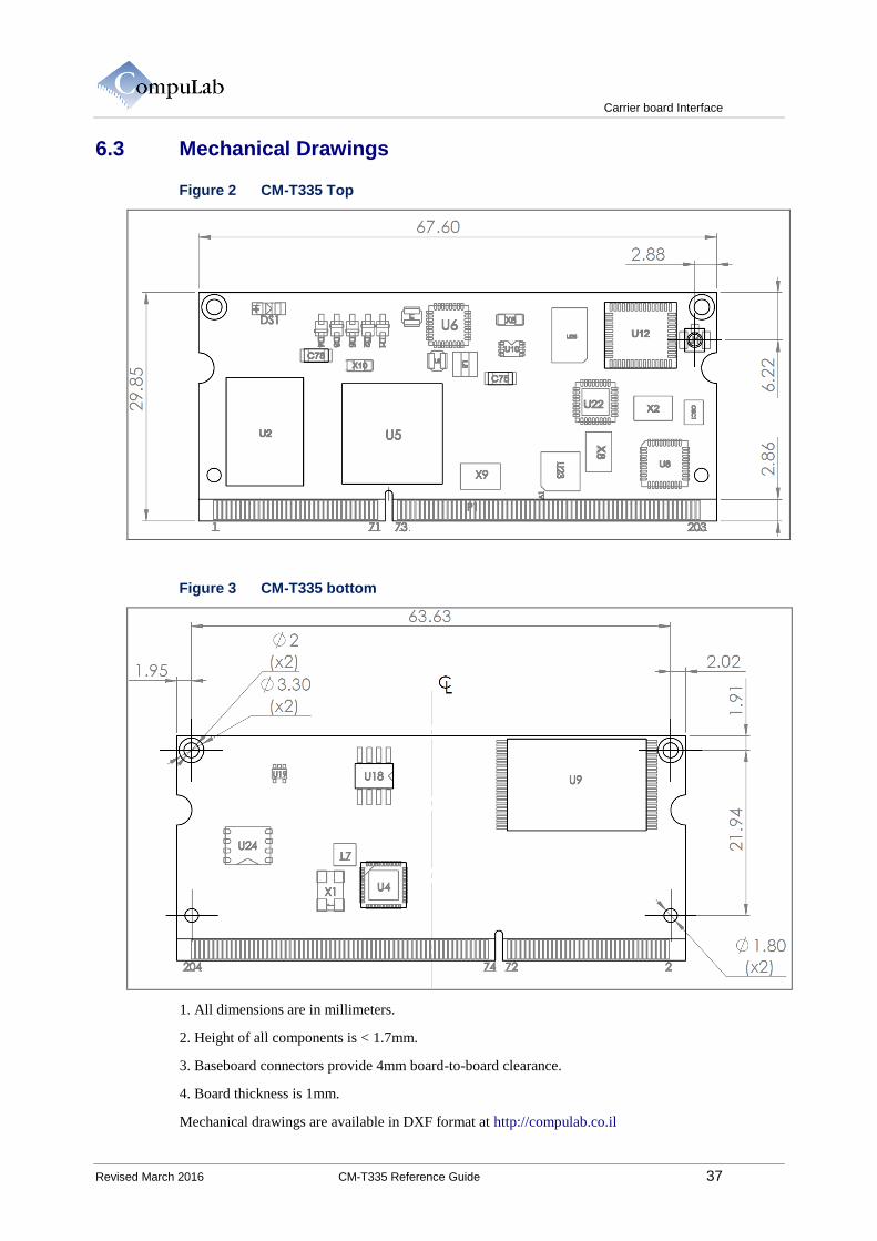
Carrier board Interface
Revised March 2016 CM-T335 Reference Guide 37
6.3 Mechanical Drawings
Figure 2 CM-T335 Top
Figure 3 CM-T335 bottom
1. All dimensions are in millimeters.
2. Height of all components is < 1.7mm.
3. Baseboard connectors provide 4mm board-to-board clearance.
4. Board thickness is 1mm.
Mechanical drawings are available in DXF format at http://compulab.co.il

Carrier board Interface
Revised March 2016 CM-T335 Reference Guide 38
6.4 Standoffs
CM-T335 has four mounting holes to physically secure the CoM to the base board. In order to secure
to base board, use two standoffs of the following specifications:
M2x0.4 thread, 2.2±0.2 mm length.
Mount the spacer with any adequate screw and nut.
Operational Characteristics
Revised March 2016 CM-T335 Reference Guide 39
7 OPERATIONAL CHARACTERISTICS
7.1 Absolute Maximum Ratings
The absolute maximum voltage ratings ate described in Table 32. Any deviation from the listed
values may result in permanent damage to the device. For recommended operating conditions see
chapter 7.2.
Table 32 Absolute Maximum ratings
Parameter Description Min Max Unit
VIN Main power supply voltage -0.3 3.6 V
VDD_RTC_BACK Backup battery supply voltage -0.3 6.0 V
USB0_VBUS USB power supply -0.5 5.25 V
VIO Input voltage at all I/O pins (steady state) -0.5 3.3 V
7.2 Recommended Operating Conditions
The recommended operating conditions are described in Table 33.
Table 33 Recommended Operating Conditions
Supply Name Description Min Typ. Max Unit
VIN Main power supply voltage 3.0 3.3 3.6 V
VDD_RTC_BACK Backup battery supply voltage 1.4 5.0 5.5 V
USB0_VBUS USB power supply 4.75 5.0 5.25 V
7.3 IO Electrical Characteristics
The I/O electrical characteristics are described in Table 34.
Table 34 DC Electrical Characteristics for multifunctional digital IO
Parameter Min Max Unit
VIH 2 3.3 V
VIL 0 0.8 V
VOH 2.85 V
VOL 0 0.45 V
Note: DC electrical characteristics listed above are generic. For specific signals characteristics,
refer to AM335x datasheet and note that VDDS_DDRx = 1.5V, VDD_COREx = 1.1V,
VSSx = 0V and VDDSHVx=3.3V.
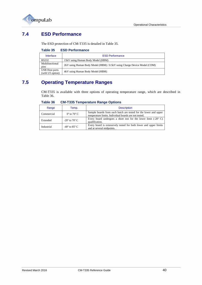
Operational Characteristics
Revised March 2016 CM-T335 Reference Guide 40
7.4 ESD Performance
The ESD protection of CM-T335 is detailed in Table 35.
Table 35 ESD Performance
Interface ESD Performance
RS232 15kV using Human Body Model (HBM)
Multifunctional
pins 2kV using Human Body Model (HBM) / 0.5kV using Charge Device Model (CDM)
USB Host ports (with U5 option)
4kV using Human Body Model (HBM)
7.5 Operating Temperature Ranges
CM-T335 is available with three options of operating temperature range, which are described in
Table 36.
Table 36 CM-T335 Temperature Range Options
Range Temp. Description
Commercial 0o to 70o C Sample boards from each batch are tested for the lower and upper
temperature limits. Individual boards are not tested.
Extended -20o to 70o C Every board undergoes a short test for the lower limit (-20o C) qualification.
Industrial -40o to 85o C Every board is extensively tested for both lower and upper limits
and at several midpoints.
Application Notes
Revised March 2016 CM-T335 Reference Guide 41
8 APPLICATION NOTES
8.1 Carrier Board Design Guidelines
Ensure that all VIN and GND power pins are connected.
Major power rails - VIN and GND must be implemented by planes, rather than traces.
Using at least two planes is essential to ensure the system signal quality, because the planes
provide a current return path for all interface signals.
It is recommended to put several 100nF and 10/100uF capacitors between VIN and GND
near the mating connectors.
It is recommended to connect the standoff holes of the carrier board to GND, in order to
improve EMC.
If a Lithium battery is connected to the VDD_RTC_BACK backup power input, a
protection resistor of value up to 1kOhm should be connected series with it. That way the
charging current should meet UL1642 standard for Lithium batteries safety. For more
information see EM3027 RTC datasheet.
Except for a power connection, no other connection is mandatory for CM-T335 operation.
All power-up circuitry and all required pullups/pulldowns are found on the module.
If for some reason you decide to place an external pullup or pulldown resistor on a certain
signal (for example - on the GPIOs), first check the documentation of that signal provided
in this manual. Certain signals have on-board pullup/pulldown resistors required for proper
initialization. Overriding their values by external components may disable board operation.
You must be familiar with signal interconnection design rules. There are many sensitive
groups of signals. For example:
Ethernet, USB and more signals must be routed in differential pairs and by a controlled
impedance trace.
Analog inputs must be decoupled from possible sources of carrier board noise.
Be careful when placing components under the CM-T335 module. The carrier board
interface connector provides 4mm mating height. Bear in mind that there are components
on the underside of the CM-T335. Maximum allowable height for components placed
under the CM-T335 is 1mm.
Refer to the SB-T335 carrier board reference design schematics.
8.2 Carrier Board Troubleshooting
Using grease solvent and a soft brush, clean the contacts of the mating connectors of both
the module and the carrier board. Remnants of soldering paste can prevent proper contact.
Take care to let the connectors and the module dry entirely before re-applying power –
otherwise corrosion may occur.
Using an oscilloscope, check the voltage levels and quality of the VIN power supply. It
should be as specified in section 7.2. Check that there is no excessive ripple or glitches.
First perform the measurements without plugging in the module. Then plug in the module
and measure again. Measurement should be performed on the pins of the mating connector.
Using an oscilloscope, verify that the GND pins of the mating connector are indeed at zero
voltage level and that there is no ground bouncing. The module must be plugged in during
the test.
Create a "minimum system" - only power, mating connectors, the module and a serial
interface.
Check if the system starts properly. In system larger than the minimum, possible sources of
disturbance could be:
Devices improperly driving the local bus
External pullup/pulldown resistors overriding the module on-board values, or any other
component creating the same "overriding" effect
Application Notes
Revised March 2016 CM-T335 Reference Guide 42
Faulty power supply
In order to avoid possible sources of disturbance, it is strongly recommended to start with a
minimal system and then to add/activate off-board devices one by one.
Check for the existence of soldering shorts between pins of mating connectors. Even if the
signals are not used on the carrier board, shorting them on the connectors can disable the
module operation. An initial check can be performed using a microscope. However, if
microscope inspection finds nothing, it is advisable to check using an X-ray, because often
solder bridges are deep beneath the connector body. Note that solder shorts are the most
probable factor to prevent a module from booting.
Check possible signal short circuits due to errors in carrier board PCB design or assembly.
Improper functioning of a customer carrier board can accidentally delete boot-up code
from the CM-T335, or even damage the module hardware permanently. Before every new
attempt of activation, check that your module is still functional with CompuLab SB-T335
carrier board.


