Helsinki University of Technology Electronic Circuit Design Laboratory Report 37, Espoo 2003 Analog Baseband Circuits for WCDMA Direct- Conversion Receivers Jarkko Jussila Dissertation for the degree of Doctor of Science in Technology to be presented with due permission of the Department of Electrical and Communications Engineering for public examination and debate in Auditorium S4 at Helsinki University of Technology (Espoo, Finland) on the 27th of June, at 12 o’clock noon. Helsinki University of Technology Department of Electrical and Communications Engineering Electronic Circuit Design Laboratory Teknillinen korkeakoulu Sähkö- ja tietoliikennetekniikan osasto Piiritekniikan laboratorio
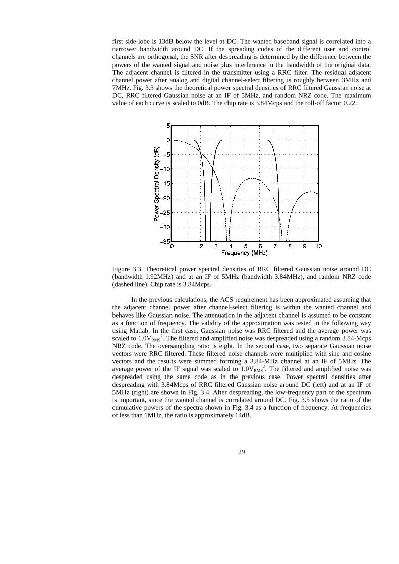
Transcript
Helsinki University of Technology Electronic Circuit Design Laboratory Report 37, Espoo 2003
Analog Baseband Circuits for WCDMA Direct-Conversion Receivers Jarkko Jussila Dissertation for the degree of Doctor of Science in Technology to be presented with due permission of the Department of Electrical and Communications Engineering for public examination and debate in Auditorium S4 at Helsinki University of Technology (Espoo, Finland) on the 27th of June, at 12 o’clock noon. Helsinki University of Technology Department of Electrical and Communications Engineering Electronic Circuit Design Laboratory Teknillinen korkeakoulu Sähkö- ja tietoliikennetekniikan osasto Piiritekniikan laboratorio
Distribution: Helsinki University of Technology Department of Electrical and Communications Engineering Electronic Circuit Design Laboratory P.O.Box 3000 FIN-02015 HUT Finland Tel. +358 9 4512271 Fax: +358 9 4512269 Copyright 2003 Jarkko Jussila ISBN 951-22-6594-X ISSN 1455-8440 Otamedia Oy Espoo 2003
i
Abstract This thesis describes the design and implementation of analog baseband circuits for low-power single-chip WCDMA direct-conversion receivers. The reference radio system throughout the thesis is UTRA/FDD. The analog baseband circuit consists of two similar channels, which contain analog channel-select filters, programmable-gain amplifiers, and circuits that remove DC offsets. The direct-conversion architecture is described and the UTRA/FDD system characteristics are summarized. The UTRA/FDD specifications define the performance requirement for the whole receiver. Therefore, the specifications for the analog baseband circuit are obtained from the receiver requirements through calculations performed by hand. When the power dissipation of an UTRA/FDD direct-conversion receiver is minimized, the design parameters of an all-pole analog channel-select filter and the following Nyquist rate analog-to-digital converter must be considered simultaneously. In this thesis, it is shown that minimum power consumption is achieved with a fifth-order lowpass filter and a 15.36-MS/s Nyquist rate converter that has a 7- or 8-bit resolution. A fifth-order Chebyshev prototype with a passband ripple of 0.01dB and a –3-dB frequency of 1.92-MHz is adopted in this thesis. The error-vector-magnitude can be significantly reduced by using a first-order 1.4-MHz allpass filter. The selected filter prototype fulfills all selectivity requirements in the analog domain. In this thesis, all the filter implementations use the opamp-RC technique to achieve insensitivity to parasitic capacitances and a high dynamic range. The adopted technique is analyzed in detail. The effect of the finite opamp unity-gain bandwidth on the filter frequency response can be compensated for by using passive methods. Compensation schemes that also track the process and temperature variations have been developed. The opamp-RC technique enables the implementation of low-voltage filters. The design and simulation results of a 1.5-V 2-MHz lowpass filter are discussed. The developed biasing scheme does not use any additional current to achieve the low-voltage operation, unlike the filter topology published previously elsewhere. Methods for removing DC offsets in UTRA/FDD direct-conversion receivers are presented. The minimum areas for cascaded AC couplings and DC-feedback loops are calculated. The distortion of the frequency response of a lowpass filter caused by a DC-feedback loop connected over the filter is calculated and a method for compensating for the distortion is developed. The time constant of an AC coupling can be increased using time-constant multipliers. This enables the implementation of AC couplings with a small silicon area. Novel time-constant multipliers suitable for systems that have a continuous reception, such as UTRA/FDD, are presented. The proposed time-constant multipliers only require one additional amplifier. In an UTRA/FDD direct-conversion receiver, the reception is continuous. In a low-power receiver, the programmable baseband gain must be changed during reception. This may produce large, slowly decaying transients that degrade the receiver performance. The thesis shows that AC-coupling networks and DC-feedback loops can be used to implement programmable-gain amplifiers, which do not produce significant transients when the gain is altered. The principles of operation, the design, and the practical implementation issues of these amplifiers are discussed. New PGA topologies suitable for continuously receiving systems have been developed. The behavior of these circuits in the presence of strong out-of-channel signals is analyzed. The interface between the downconversion mixers and the analog baseband circuit is discussed. The effect of the interface on the receiver noise figure and the trimming of mixer IIP2 are analyzed. The design and implementation of analog baseband circuits and channel-select filters for UTRA/FDD direct-conversion receivers are discussed in five application cases.
ii
The first case presents the analog baseband circuit for a chip-set receiver. A channel-select filter that has an improved dynamic range with a smaller supply current is presented next. The third and fifth application cases describe embedded analog baseband circuits for single-chip receivers. In the fifth case, the dual-mode analog baseband circuit of a quad-mode receiver designed for GSM900, DCS1800, PCS1900, and UTRA/FDD cellular systems is described. A new, highly linear low-power transconductor is presented in the fourth application case. The fourth application case also describes a channel-select filter. The filter achieves +99-dBV out-of-channel IIP2, +45-dBV out-of-channel IIP3 and 23-µVRMS input-referred noise with 2.6-mA current from a 2.7-V supply. In the fifth application case, a corresponding performance is achieved in UTRA/FDD mode. The out-of-channel IIP2 values of approximately +100dBV achieved in this work are the best reported so far. This is also the case with the figure of merits for the analog channel-select filter and analog baseband circuit described in the fourth and fifth application cases, respectively. For equal power dissipation, bandwidth, and filter order, these circuits achieve approximately 10dB and 15dB higher spurious-free dynamic ranges, respectively, when compared to implementations that are published elsewhere and have the second best figure of merits.
iii
Preface The research for this thesis has been carried out in the Electronic Circuit Design Laboratory of Helsinki University of Technology between 1997 and 2002. The work presented in this thesis is part of a research project funded by Nokia Networks, Nokia Mobile Phones, and Finnish National Technology Agency (TEKES). For four years, I had the priviledge of being a postgraduate student in the Graduate School in Electronics, Telecommunications, and Automation (GETA), which partially funded my studies. I also thank the following foundations for financial support: Nokia Foundation, the Finnish Society of Electronics Engineers (EIS), Emil Aaltonen Foundation, the Foundation of Technology (TES), and the Foundation for Financial Aid at the Helsinki University of Technology. I would like to thank my supervisor Prof. Kari Halonen for the opportunity to work on an interesting research topic and his encouragement and guidance during the research. Prof. Mohammed Ismail and Prof. Kenneth Martin are acknowledged for reviewing my thesis. I would also like to thank Timo Knuuttila for proposing the research project on direct-conversion radio receivers. I want to express my gratitude to all my present and former colleaques at the laboratory for creating a relaxed and pleasant working atmosphere. I wish to thank Dr. Saska Lindfors for his valuable advices and instructions and for teaching me a lot of things about the design of CMOS baseband circuits. I am grateful to Dr. Aarno Pärssinen for his important advices and guidance in the field of integrated radio receiver design. In addition, I would like to thank Rami Ahola, Mikko Hirvonen, Tuomas Hollman, and Jarkko Routama for their valuable help during the project. The members of the research team “SuMu”, Dr. Kalle Kivekäs, Dr. Aarno Pärssinen, Jussi Ryynänen, and Dr. Lauri Sumanen, deserve special thanks for creating an excellent working atmosphere. Their help and contributions and the relaxed, humorous, and inspiring team spirit have been essential for this work. In addition, the junior researchers of the direct-conversion receiver projects, Jere Järvinen, Mikko Hotti, and Jouni Kaukovuori, deserve a mention. My warmest thanks go to my parents Pirjo and Tauno and my sister Virve for their support and encouragement during my studies. My friends deserve big thanks for free time activities that have formed excellent counterbalance for work. Jarkko Jussila Espoo, June 2003
iv
Symbols a Constant a0 DC offset a1 Linear gain a2, a3, … Nonlinearity coefficients a(t) Amplitude-modulated part of the signal A Mean value of the amplitude-modulated part of the signal, voltage gain,
amplifier, capacitor or resistor area AV Voltage gain B Equivalent RF noise bandwidth of the channel C Capacitor, capacitance CC Compensation capacitor CE Absolute capacitance error CLSB Capacitor corresponding to the least significant bit in a capacitor matrix C0 Capacitor corresponding to the minimum value of a capacitor matrix d1 - dN N-bit digital control signal DC Capacitance density DR Resistance density Eb Bit energy Econv Energy required for a single analog-to-digital conversion f Frequency f1, f2, fW Signal frequencies fBL Blocker frequency fBW Signal bandwidth fC Chip rate, cutoff frequency of a lowpass filter fCW Frequency of a CW blocker fD Data or symbol rate fG Frequency at which the gain of the receiver is defined at baseband fIF Intermediate frequency fIM Image frequency fLO Local oscillator frequency fP Pole frequency fsig Signal frequency fRF Radio frequency fS Sample rate fTX,L Center frequency of the transmitter leakage fT Unity-gain frequency gm Transconductance G Voltage gain, mode-select signal GC Coding gain CF Floating capacitor Gm Transconductor Gm-C Filter technique that uses transconductors and capacitors Gm-C-OTA Filter technique that uses transconductors, capacitors, and OTAs GSPR Spreading gain GV, GVOLT Voltage gain h Impulse response hI Impulse response of the I-channel filter
v
hQ Impulse response of the Q-channel filter H Transfer function in s-domain I In-phase, DC current, interference power spectral density i AC current I(t) Transmitted I- channel signal component IC Collector current of a bipolar transistor icm Common-mode current ∆icm Imbalance in common-mode current IDS Drain-source current of a MOSFET IL Current source, bias current IMIX DC current at the mixer output
ni Current-noise density k Boltzmann’s constant ≈ 1.3807⋅10-23J/K, sampling instant k1, k2 , k3 Coefficients kCMOD Empirical factor that takes into account the crest factor and signal bandwidth,
constant that describes the power variation of an interfering signal L Inductor, inductance, attenuation, effective channel length of a MOSFET LIMP Implementation loss M Margin, MOSFET MOSFET-C Filter technique that uses MOSFETs, capacitors, and amplifiers n Index N Number of symbols, harmonic components, bits, or cascaded highpass filters N0 Noise power spectral density nP Number of poles opamp-RC Filter technique using operational amplifiers, resistors, and capacitors p Pole P Power PAV Mean value of the power PD Power dissipation PDPCH Power of dedicated physical channel (DPCH) at the UE antenna connector PS+N Power of in-channel signal and interference PEQ Power of an equivalent test signal PI Total interference power before despreading PIN Input power PIMD Power of intermodulation distortion product PIMD2 Power of second-order intermodulation distortion component PIMD3 Power of third-order intermodulation distortion component PIoac Power of modulated adjacent channel PÎor Power of down-link channel at the UE antenna connector PN Noise power PPEAK 99.9% limit of the instantaneous-power distribution PTX,L Transmitter leakage power P1, P2 Powers of interfering signals Q Quadrature-phase, quality factor, bipolar transistor Q(t) Transmitted Q-channel signal component R Resistor, resistance rcas Output resistance of a cascode current source R(k) Complex number representing the ideal reference symbol RL Load resistor, load resistance RS Source resistance, resistance per square S Switch
vi
S(k) Complex number representing the actual received symbol S11 Scattering parameter of two-port (reflection) SNRIN Signal-to-noise ratio before despreading SNROUT Signal-to-noise ratio after despreading t Time T Absolute temperature TD Symbol period V DC voltage, signal amplitude v AC voltage V1, V2, VW Signal amplitudes VBL Blocker amplitude VC Controlling voltage VCC, VDD Positive supply voltage VDS,sat Drain-source saturation voltage VGS Gate-source voltage of a MOSFET VGSM Mode-select signal VM Mode-select signal vsig Wanted signal VT Thermal voltage VTH Threshold voltage of a MOSFET
nv Voltage-noise density Viip2 RMS-voltage corresponding to IIP2 Viip3 RMS-voltage corresponding to IIP3 vIMD2 Second-order intermodulation distortion component vIMD3 Third-order intermodulation distortion component VEQ,RMS RMS value of an equivalent test signal vin Input signal vout Output signal VI(t) Downconverted received signal in the I-channel VQ(t) Downconverted received signal in the Q-channel VIQ(t) Received signal W Effective channel width of a MOSFET z Zero α Roll-off factor, phase shift β Transistor parameter ε Relative inaccuracy τ Group delay ω Angular frequency ωint Unity-gain frequency of the integrator ωGBW Unity-gain frequency of the opamp ξ Crest factor ∆α Phase error ∆ACM Change in small-signal gain ∆C Change in capacitance ∆G Gain mismatch ∆GBB Variable voltage gain range at baseband ∆GBB,MAX Maximum variable voltage gain range at baseband ∆GRF Variable voltage gain range in the RF front-end ∆arms Effective magnitude ripple ∆ϕrms Effective phase ripple
vii
∆P Power difference ∆R Change in resistance ∆VOUT Voltage drop over the mixer load resistor φ Phase φ(t) Phase-modulated part of the signal
Abbreviations AC Alternating current ACA Adjacent channel attenuation ACS Adjacent channel selectivity ACLR Adjacent channel leakage ratio ADC Analog-to-digital converter AGC Automatic gain control BDR Blocking dynamic range BiCMOS Bipolar complementary metal oxide semiconductor BER Bit error rate CDMA Code division multiple access CMFB Common-mode feedback CMOS Complementary metal oxide semiconductor CMRR Common-mode rejection ratio CW Continuous wave DAC Digital-to-analog converter DC Direct current DCS1800 Digital cellular system DECT Digital enhanced cordless telecommunications DNL Differential nonlinearity DSP Digital signal processor DSB Double sideband DS Direct sequence ENOB Effective number of bits ESD Electrostatic discharge EVM Error vector magnitude FIR Finite impulse response FDD Frequency division duplex FET Field-effect transistor FoM Figure of merit FSK Frequency shift keying GSM, GSM900 Global system for mobile communications HPF Highpass filter IC Integrated circuit ICP Input compression point IF Intermediate frequency IIP2 Second-order input intercept point IIP3 Third-order input intercept point INL Integral nonlinearity IS-95 Interim standard 95 ISI Inter symbol interference ISM Industrial, scientific, medical
viii
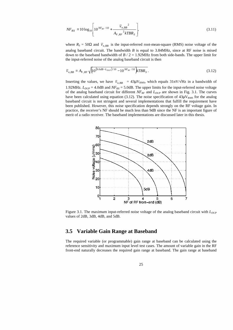
ITU International Telecommunications Union LC Inductor-capacitor LNA Low noise amplifier LO Local oscillator LSB Least significant bit MIM Metal-insulator-metal MOS Metal oxide semiconductor MOSFET Metal oxide semiconductor field effect transistor NF Noise figure NRZ Non-return-to-zero NMOS N-channel metal oxide semiconductor OF Orthogonality factor OIP2 Second-order output intercept point OIP3 Third-order output intercept point opamp Operational amplifier OTA Operational transconductance amplifier PCB Printed circuit board PCS1900 Digital cellular system PDC Personal digital cellular PGA Programmable-gain amplifier PHS Personal handy phone system PMOS P-channel metal oxide semiconductor PSRR Power-supply rejection ratio PTAT Proportional to absolute temperature QPSK Quadrature phase shift keying RC Resistor-capacitor, raised-cosine RC-PP Resistor-capacitor polyphase filter RF Radio frequency RMS Root-mean-square RRC Root-raised-cosine RX Receiver SAW Surface acoustic wave SC Switched capacitor SFG Signal flow graph SFDR Spurious free dynamic range SiGe Silicon-germanium SNDR Signal-to-noise and distortion ratio SNR Signal-to-noise ratio SSB Single sideband TDMA Time division multiple access THD Total harmonic distortion TX Transmitter UE User equipment UMTS Universal mobile telecommunications sytem UTRA UMTS terrestrial radio access VCCS Voltage controlled current source VCVS Voltage controlled voltage source VCO Voltage controlled oscillator VGA Variable-gain amplifier WCDMA Wide-band code division multiple access WLAN Wireless local area network
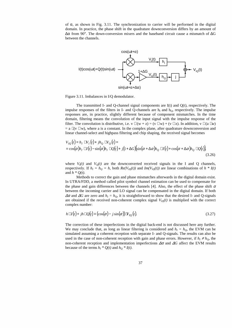
ix
WLL Wireless local loop 2G Second generation 3G Third generation 3GPP Third generation partnership project
x
Contents Abstract.................................................................................................................................... i Preface ..................................................................................................................................... iii Symbols ................................................................................................................................... iv Abbreviations........................................................................................................................... vii 1 Introduction........................................................................................................................ 1
1.1 Motivation.................................................................................................................. 1 1.2 Research Contribution and Publications..................................................................... 2 1.3 Organization of the Thesis ......................................................................................... 5
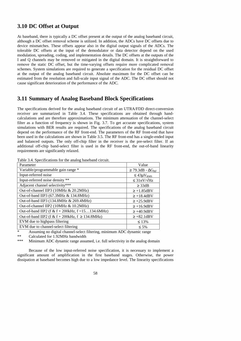
3.10 DC Offset at Output ................................................................................................... 58 3.11 Summary of Analog Baseband Block Specifications ................................................. 58
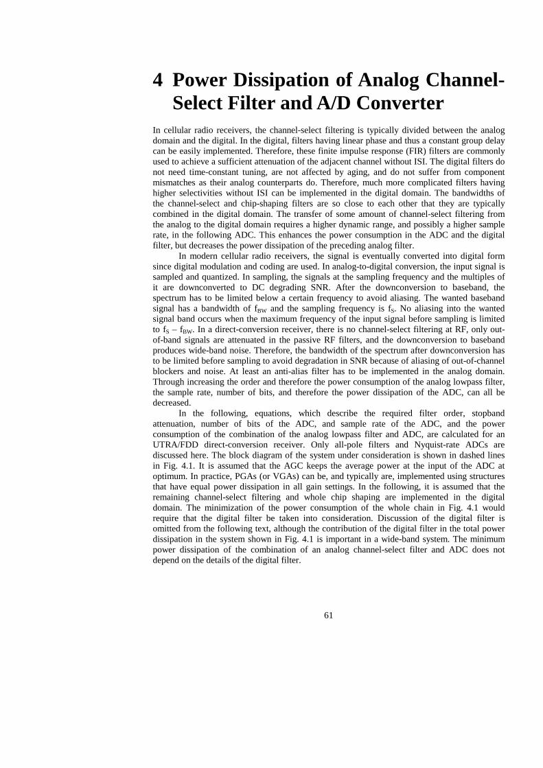
4 Power Dissipation of Analog Channel-Select Filter and A/D Converter............................ 61
xi
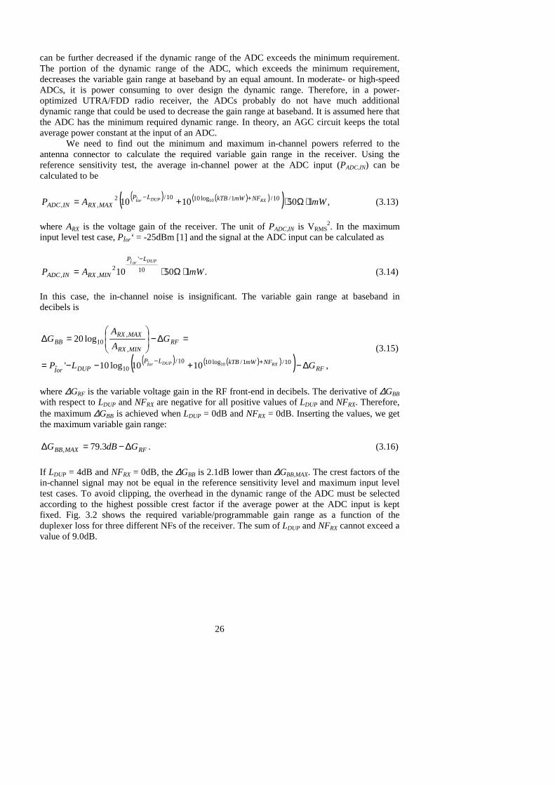
4.1 Power Dissipation of Nyquist-Rate A/D Converter ....................................................62 4.2 Power Dissipation of All-Pole Lowpass Filter............................................................62 4.3 Order of All-Pole Lowpass Filter................................................................................63 4.4 Total Power Dissipation..............................................................................................64 4.5 Performance Requirements in the Presence of Adjacent Channel Signal ...................68
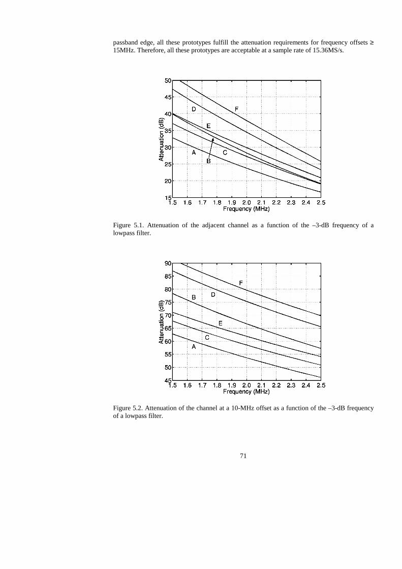
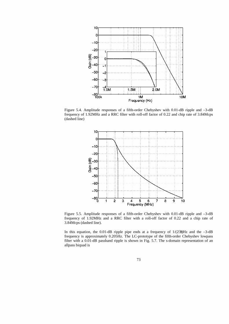
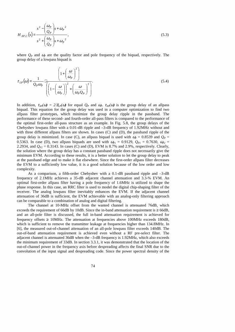
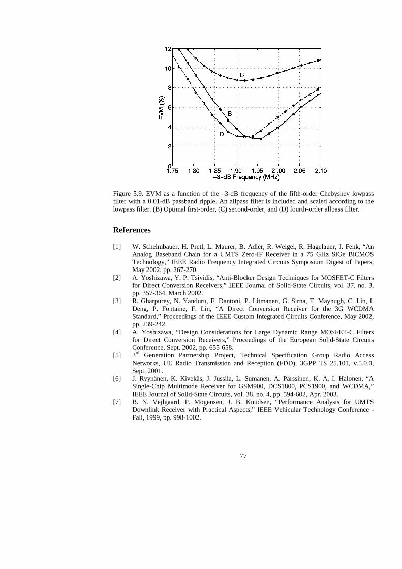
5 Prototype of Analog Channel-Select Filter .........................................................................70 6 Integrated Opamp-RC Lowpass Filters...............................................................................79
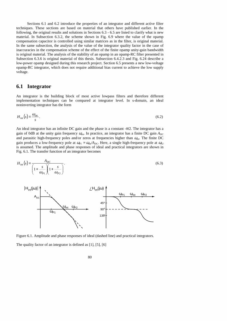
6.1 Integrator ....................................................................................................................80 6.2 Continuous-Time Active Filter Techniques ................................................................81
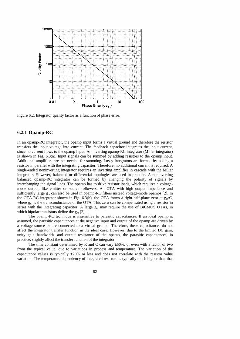
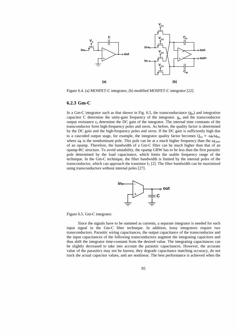
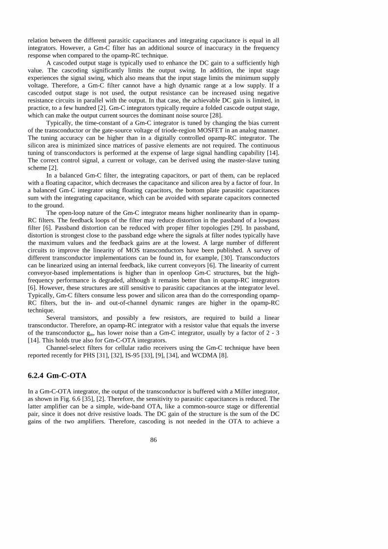
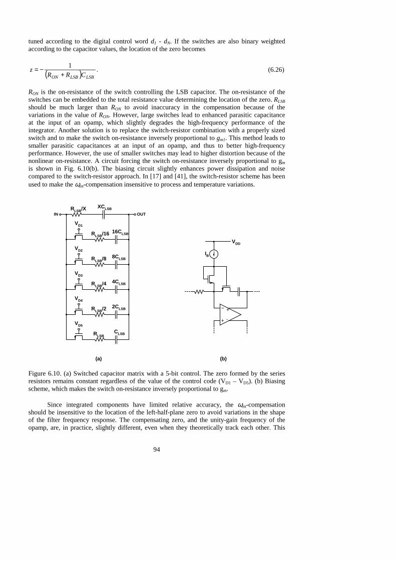
6.2.1 Opamp-RC.......................................................................................................82 6.2.2 MOSFET-C .....................................................................................................84 6.2.3 Gm-C...............................................................................................................85 6.2.4 Gm-C-OTA......................................................................................................86 6.2.5 Other Techniques Reported for WCDMA Applications..................................87
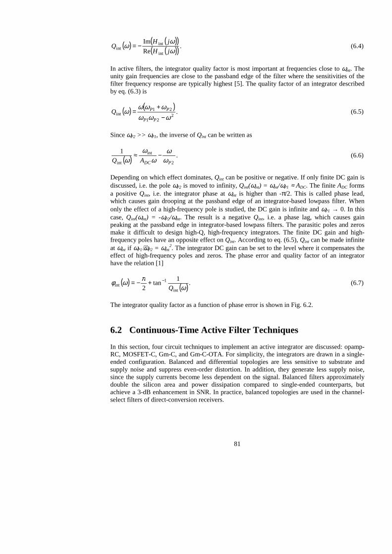
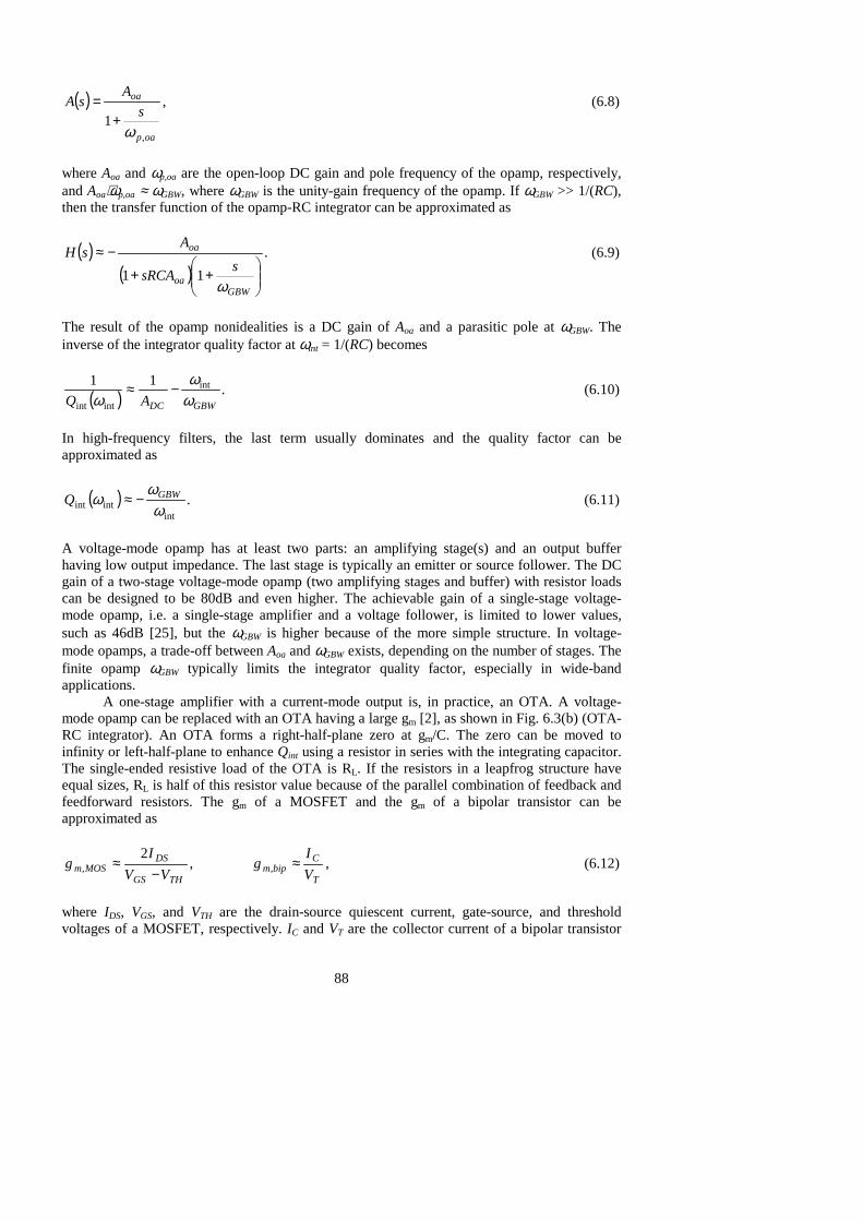
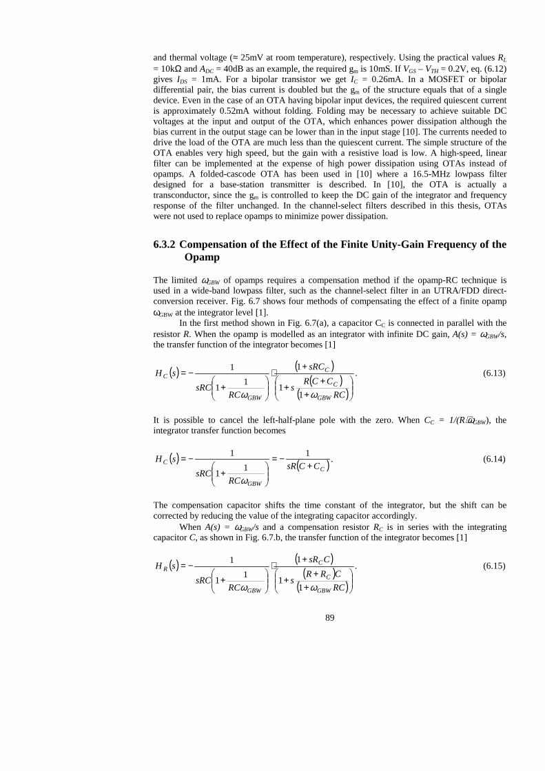
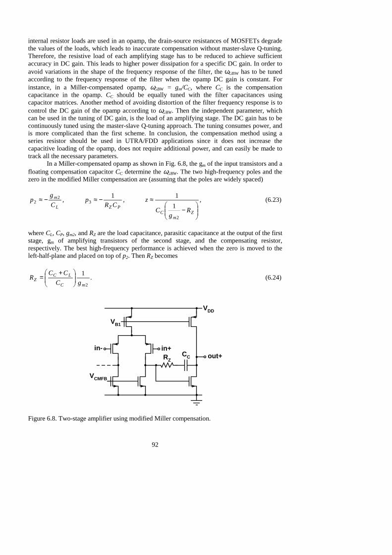
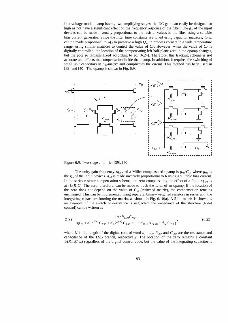
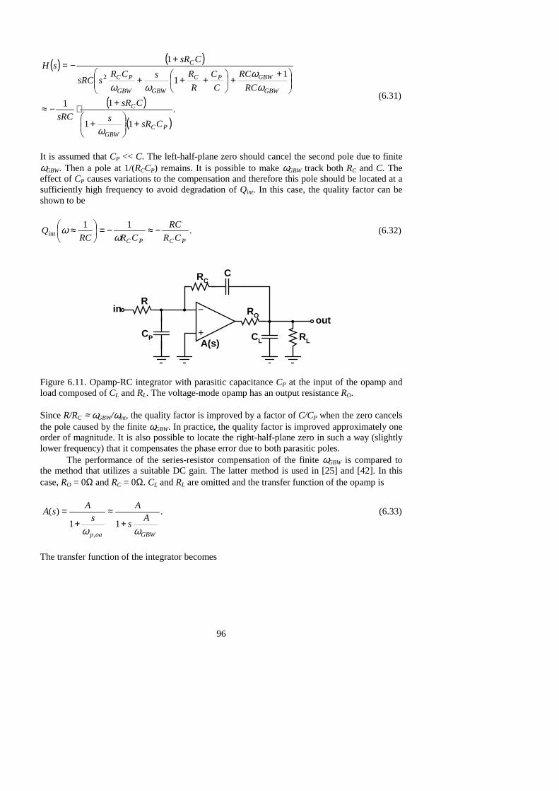
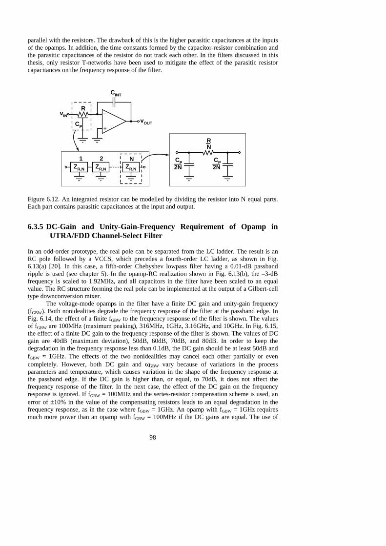
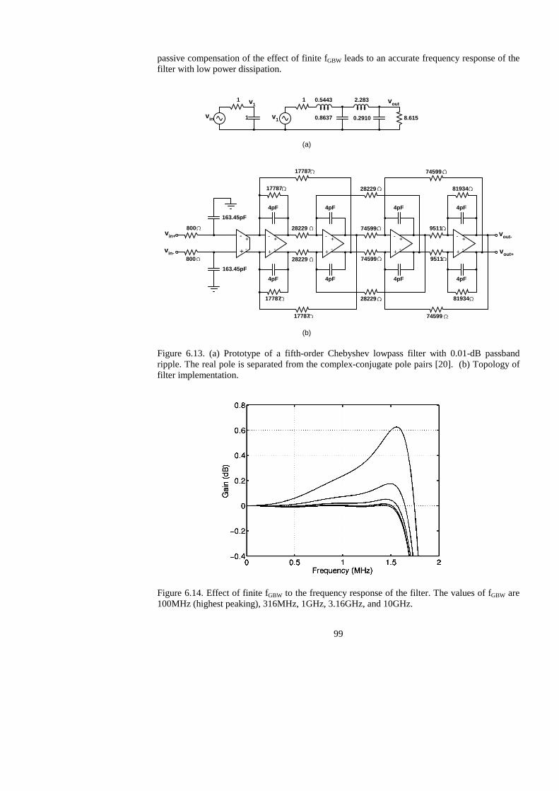
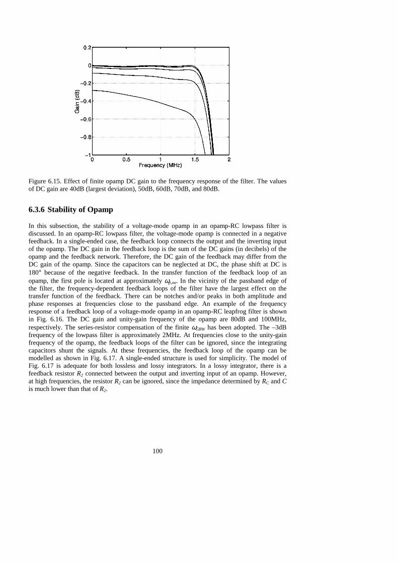
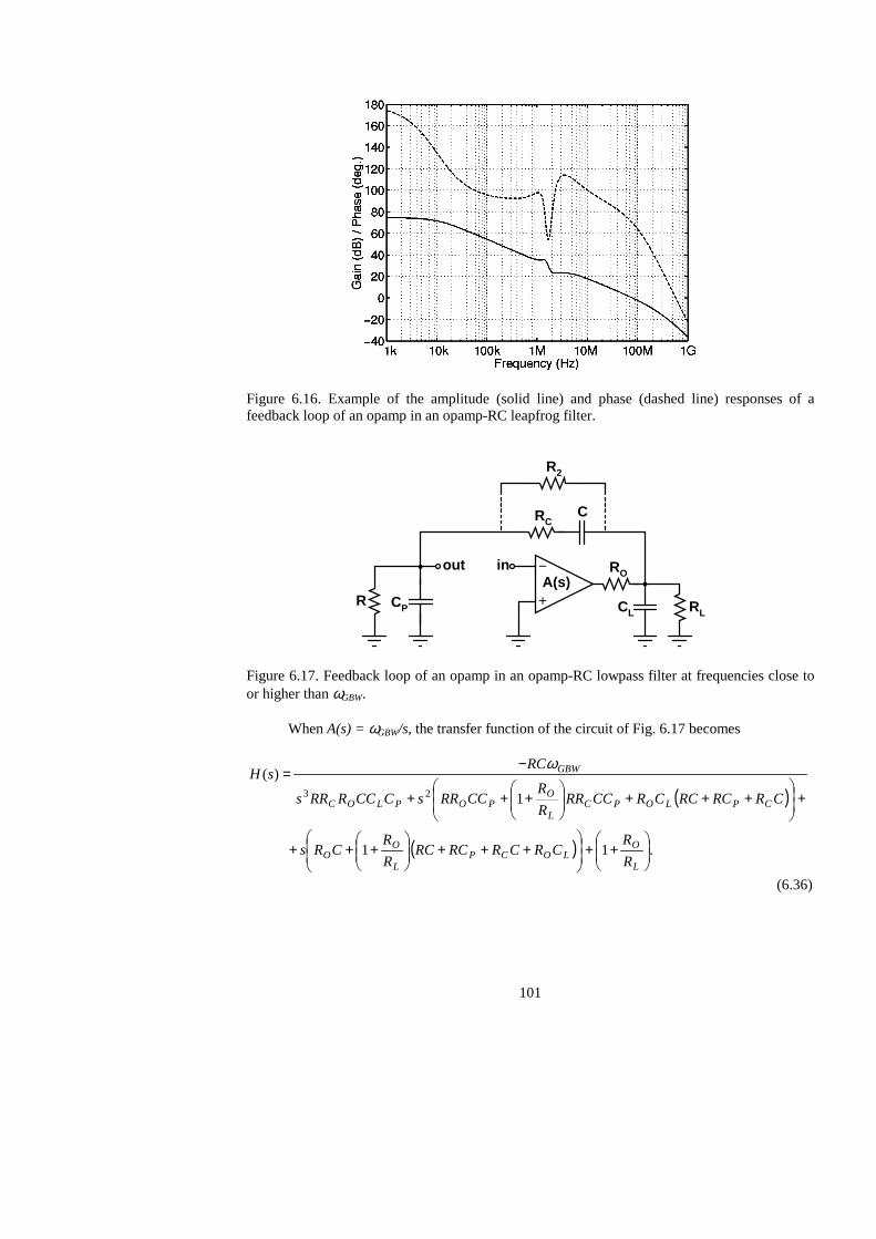
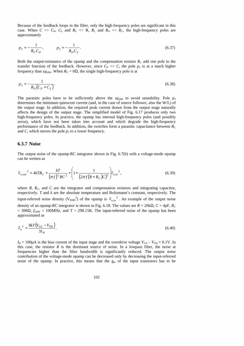
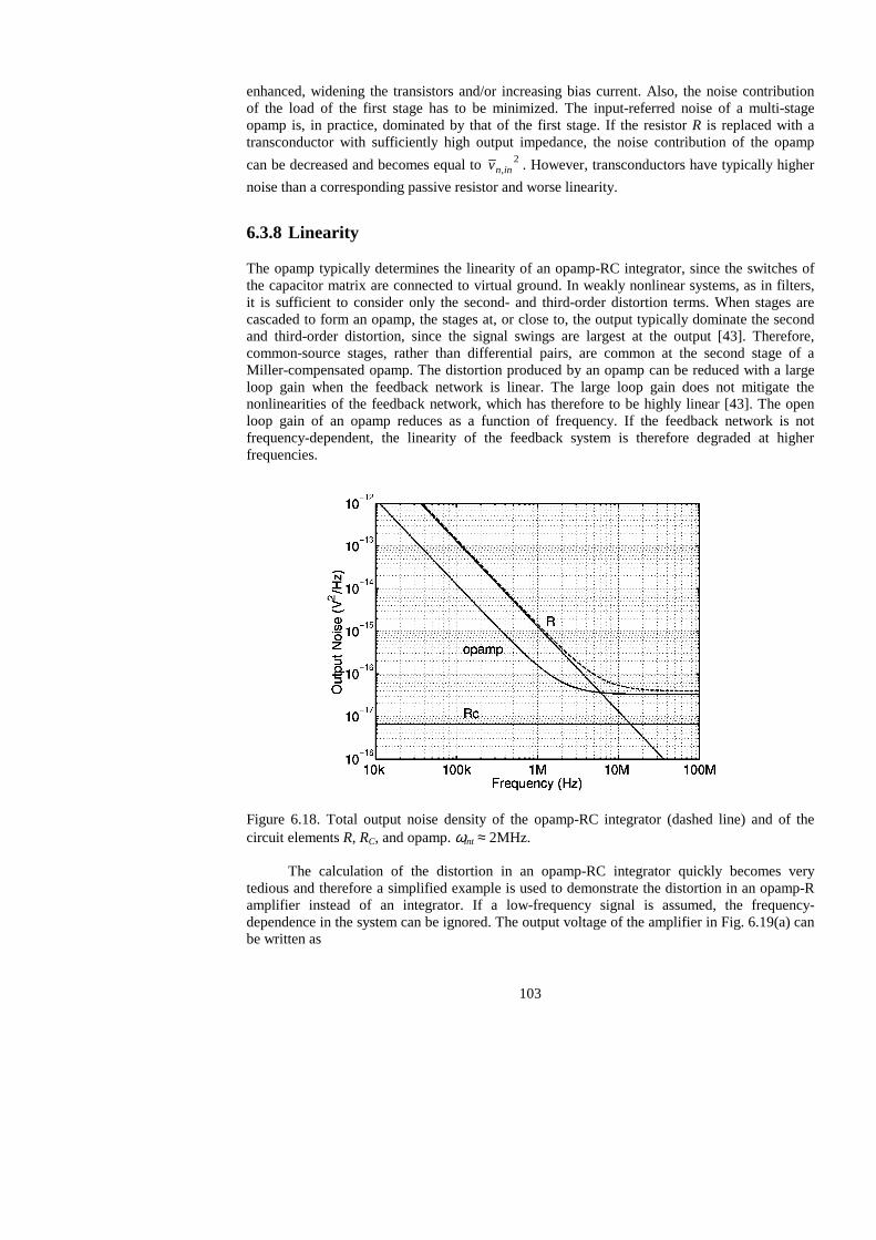
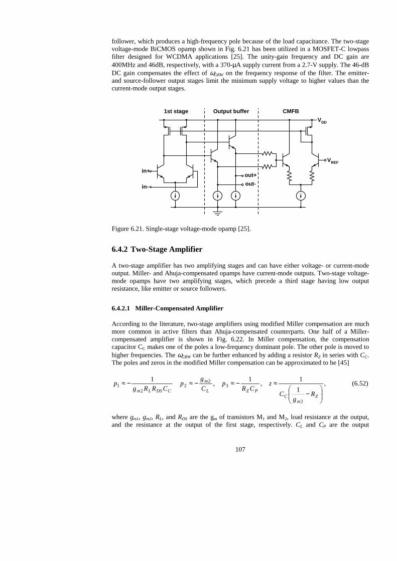
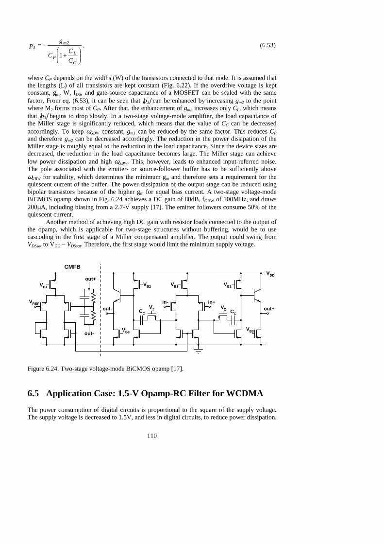
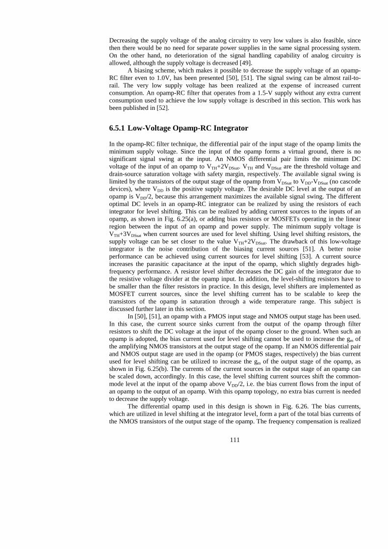
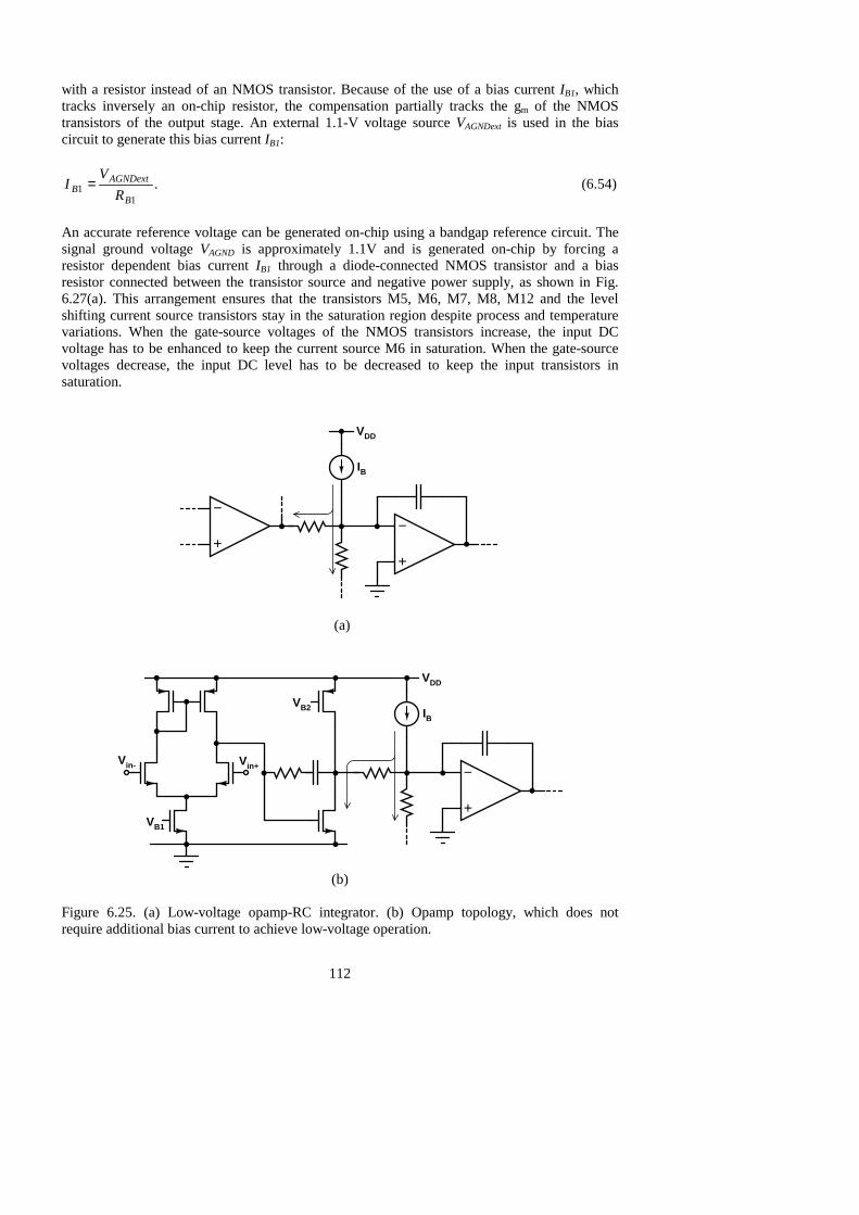
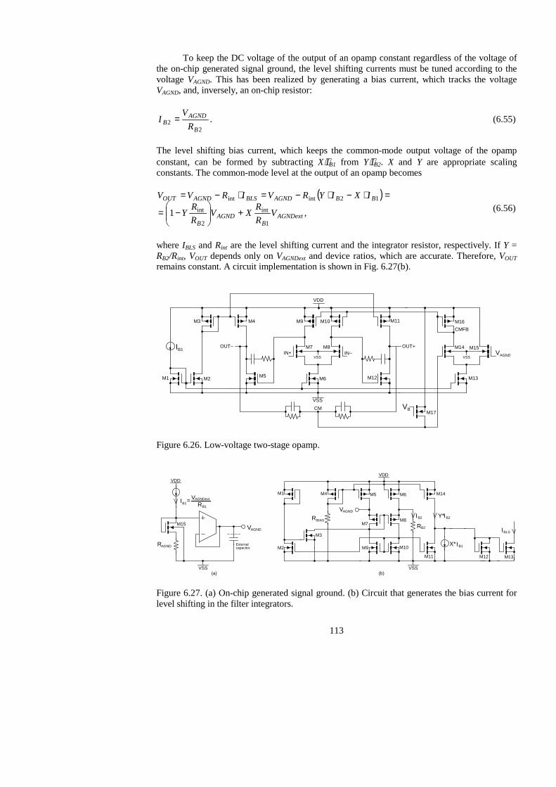
6.3 Opamp-RC Integrator .................................................................................................87 6.3.1 Quality Factor..................................................................................................87 6.3.2 Compensation of the Effect of the Finite Unity-Gain Frequency of the Opamp .............................................................................................................89 6.3.3 Opamp-RC Integrator with Parasitic Capacitances..........................................95 6.3.4 Nonidealities of Resistors and Capacitors .......................................................97 6.3.5 DC-Gain and Unity-Gain-Frequency Requirement of Opamp in UTRA/FDD Channel-Select Filter ..................................................................98 6.3.6 Stability of Opamp...........................................................................................100 6.3.7 Noise................................................................................................................102 6.3.8 Linearity ..........................................................................................................103
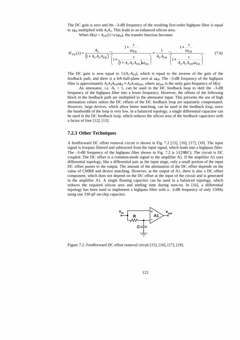
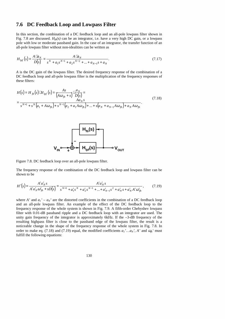
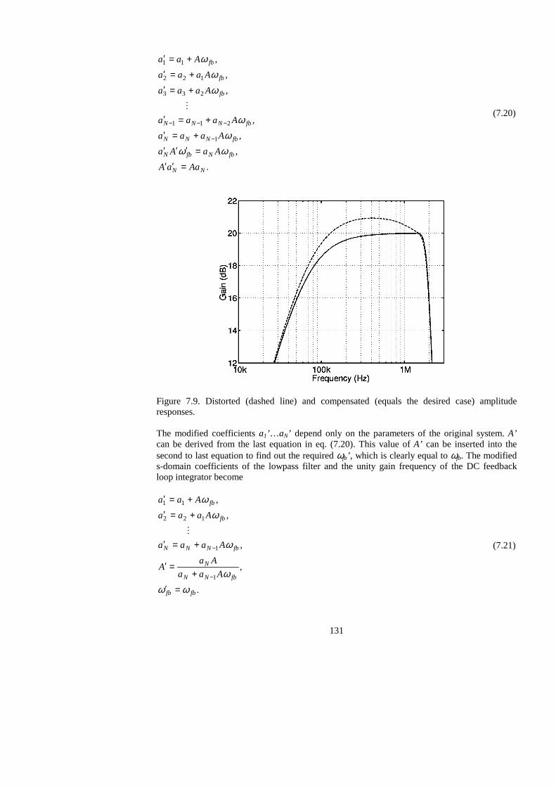
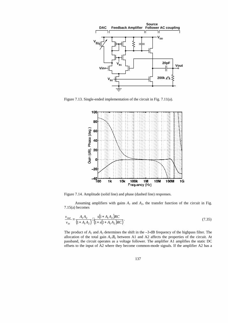
7 DC Offset Compensation in UTRA/FDD Direct-Conversion Receivers ............................119 7.1 DC Offset Compensation in Burst-Mode Reception...................................................119 7.2 DC Offset Compensation in Continuous Reception....................................................120
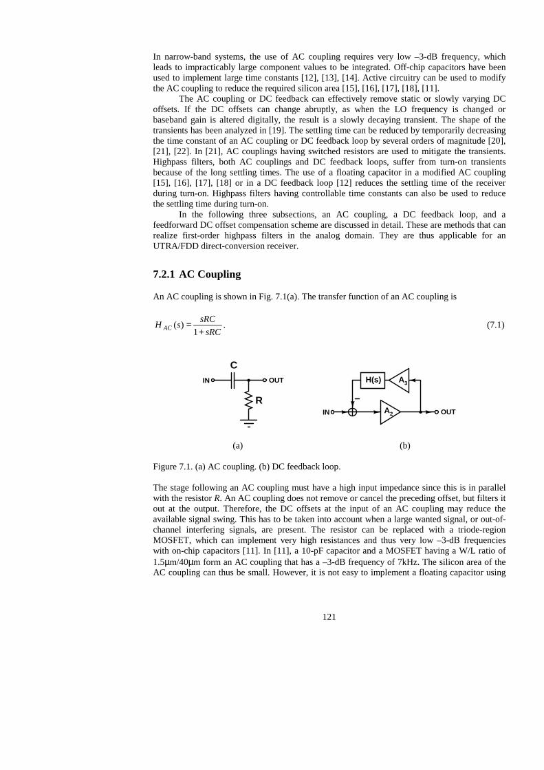
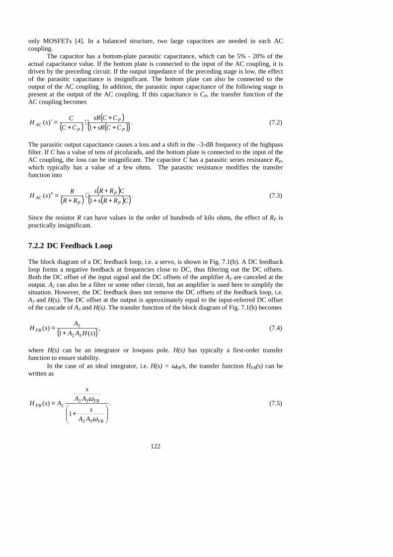
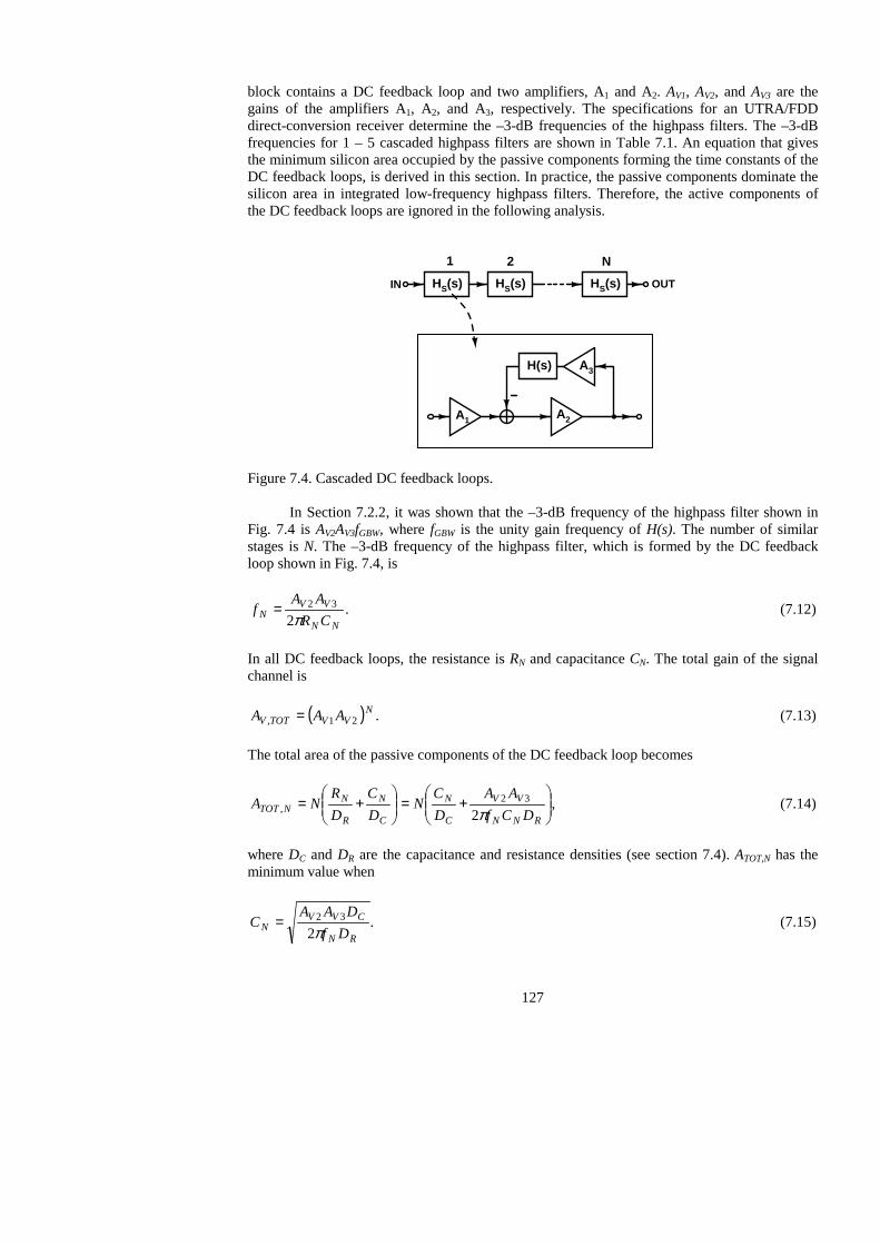
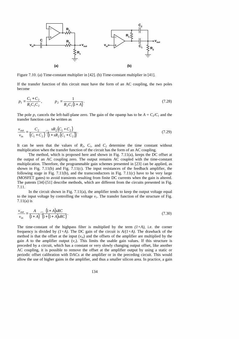
7.2.1 AC Coupling....................................................................................................121 7.2.2 DC Feedback Loop..........................................................................................122 7.2.3 Other Techniques.............................................................................................123
7.3 DC Offset Compensation in UTRA/FDD Direct-Conversion Receivers ....................124 7.4 Area of Cascaded AC Couplings ................................................................................125 7.5 Area of Cascaded DC Feedback Loops ......................................................................126 7.6 DC Feedback Loop and Lowpass Filter......................................................................130 7.7 Time-Constant Multiplier for AC Coupling................................................................133 7.8 Comparison.................................................................................................................139
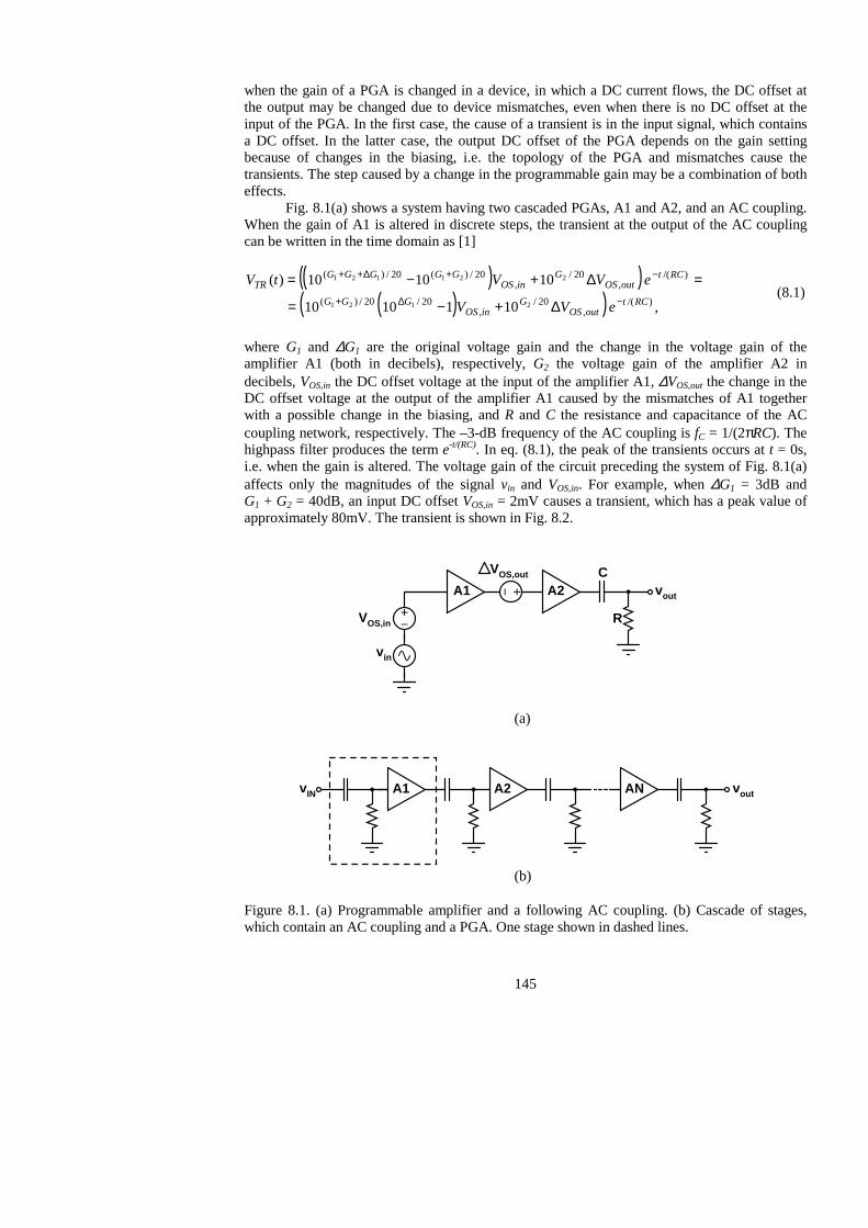
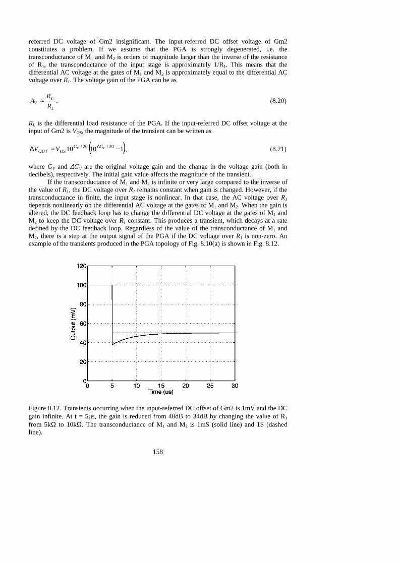
8 Programmable-Gain Amplifiers for Systems Having Continuous Reception .....................144 8.1 Transients Caused by Programmable-Gain Amplifiers...............................................144
xii
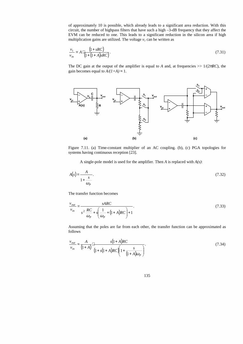
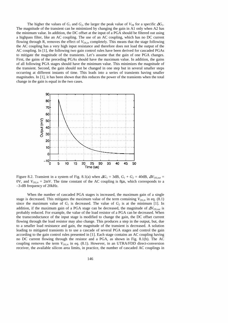
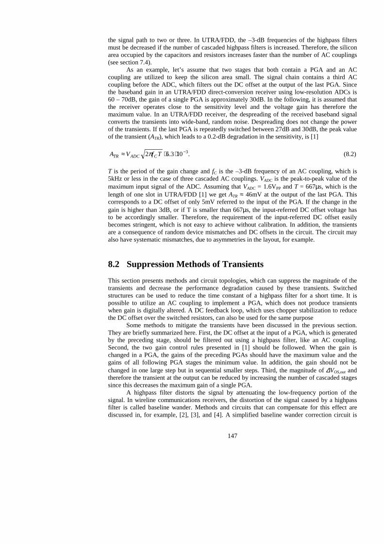
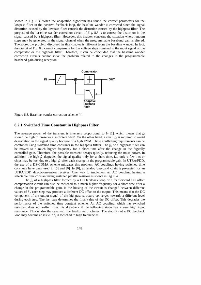
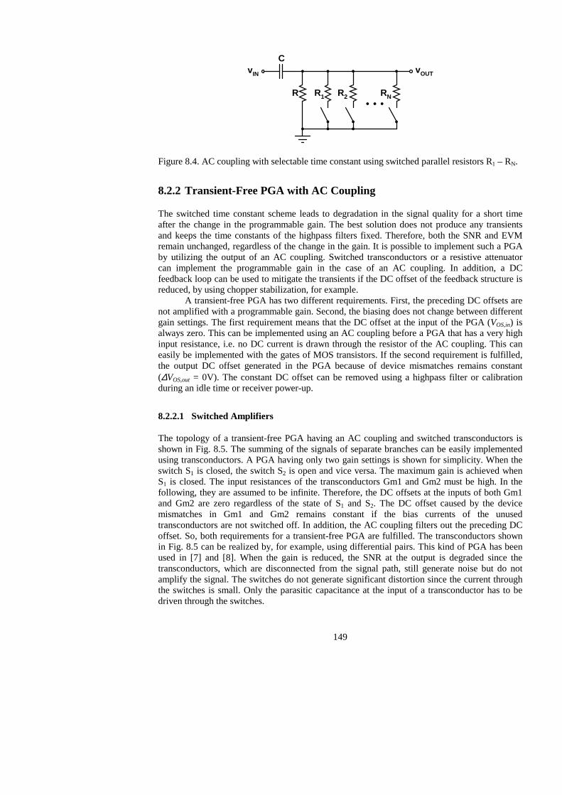
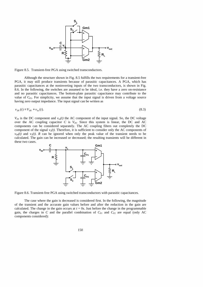
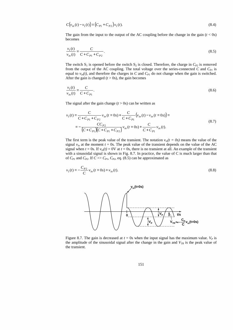
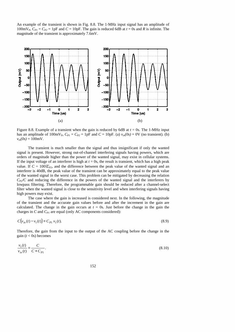
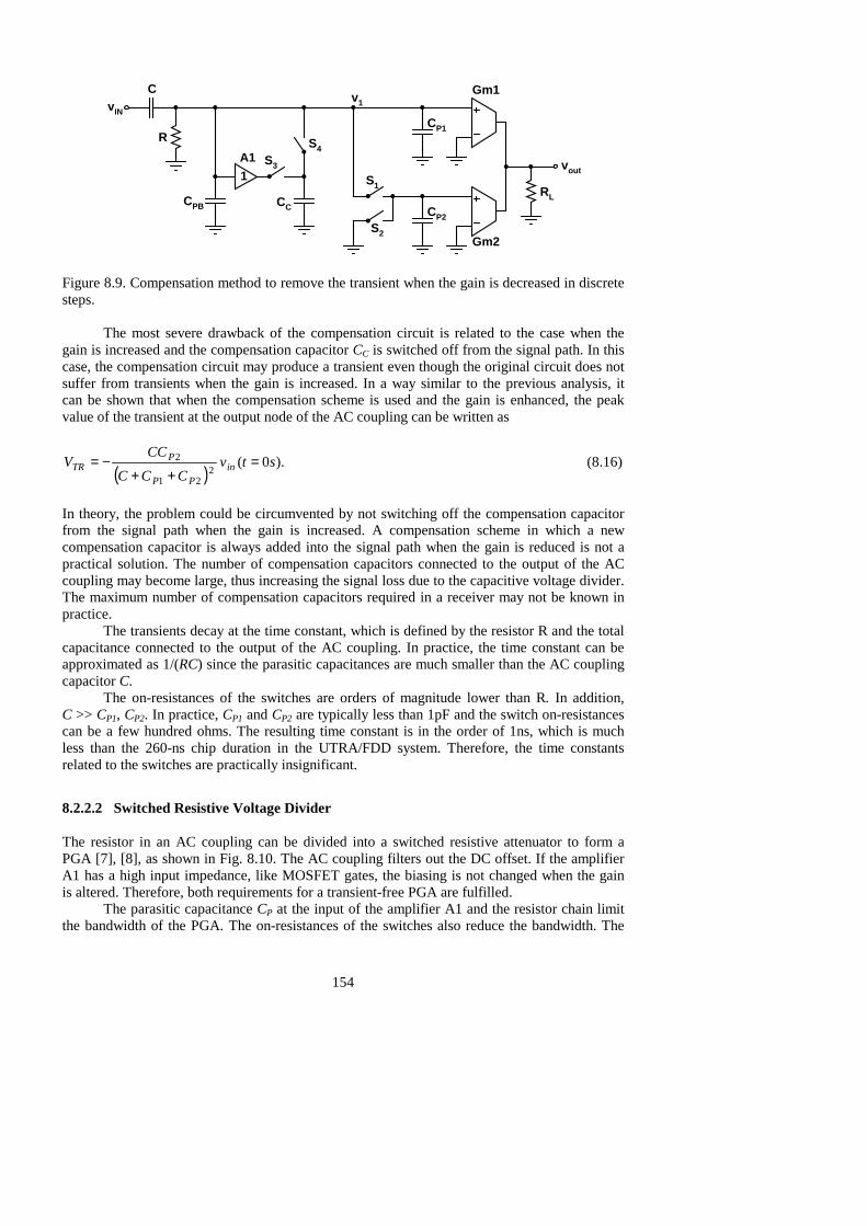
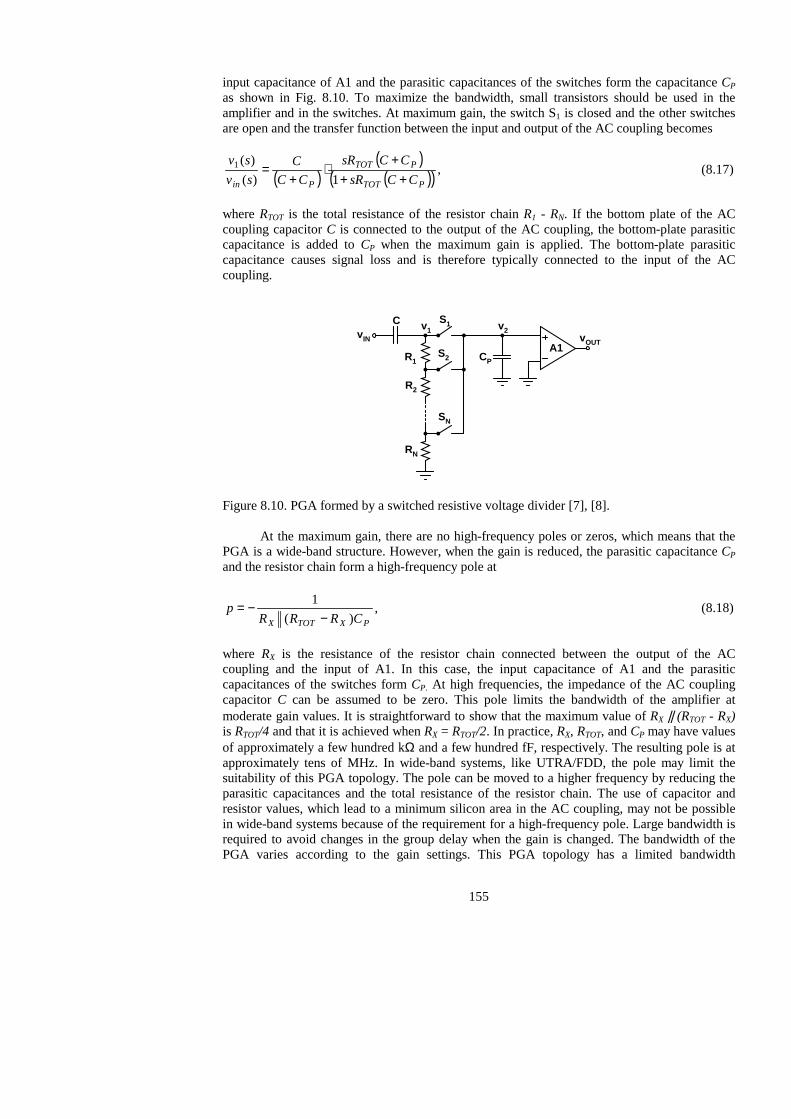
8.2 Suppression Methods of Transients............................................................................ 147 8.2.1 Switched Time Constant in Highpass Filter .................................................... 148 8.2.2 Transient-Free PGA with AC Coupling .......................................................... 149
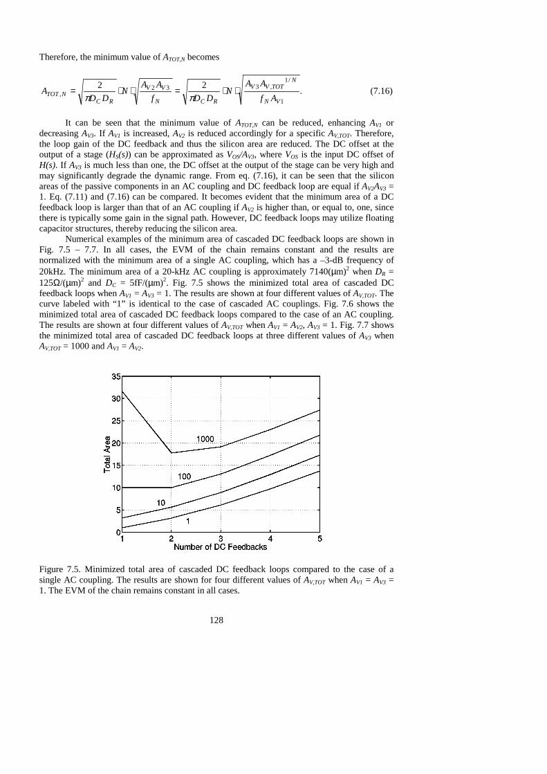
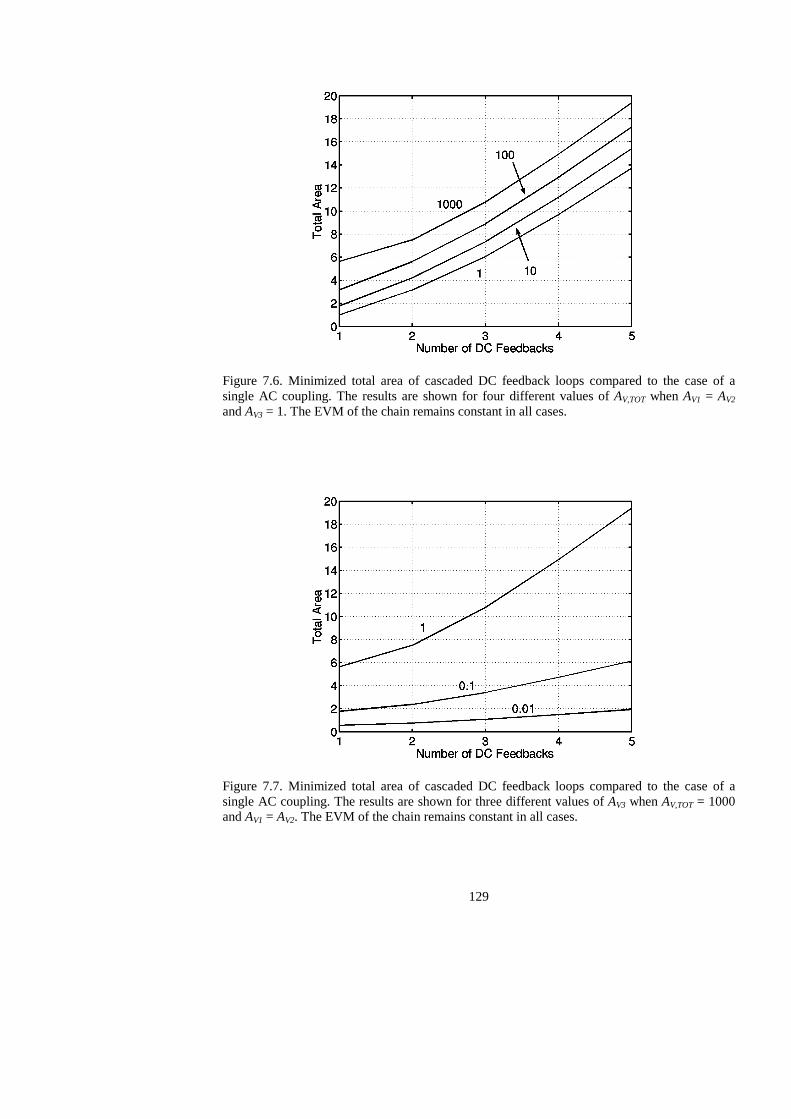
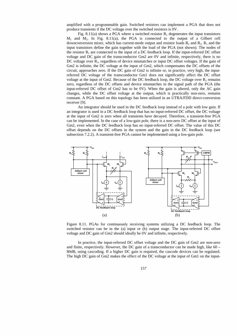
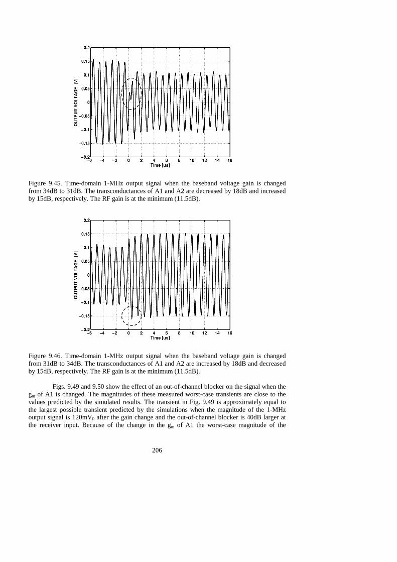
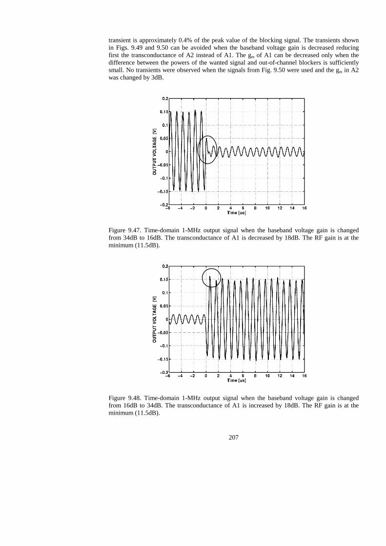
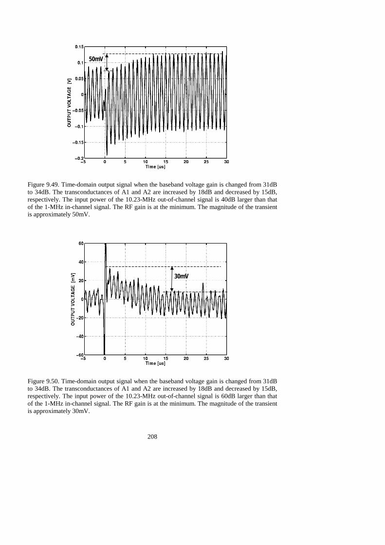
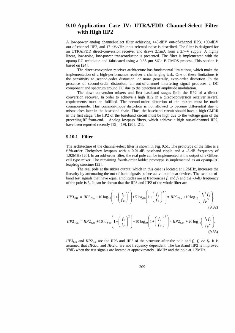
8.2.3 Transient-Free PGA with DC Feedback Loop ................................................ 156 9 Analog Baseband Circuits for UTRA/FDD Direct-Conversion Receivers......................... 162
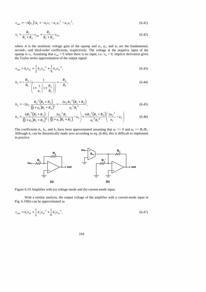
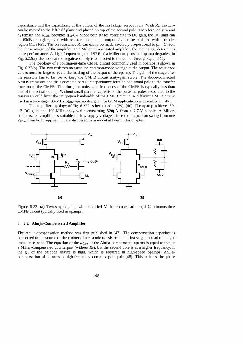
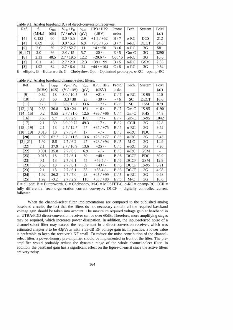
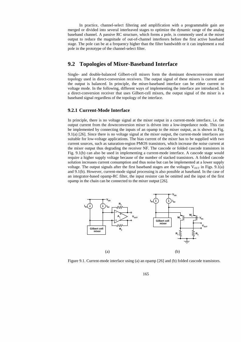
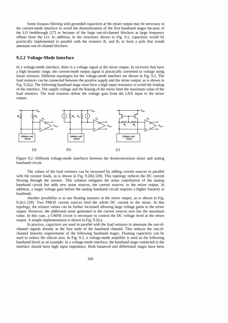
9.1 Summary of Published Analog Baseband Circuits and Channel-Select Filters .......... 163 9.2 Topologies of Mixer-Baseband Interface................................................................... 165
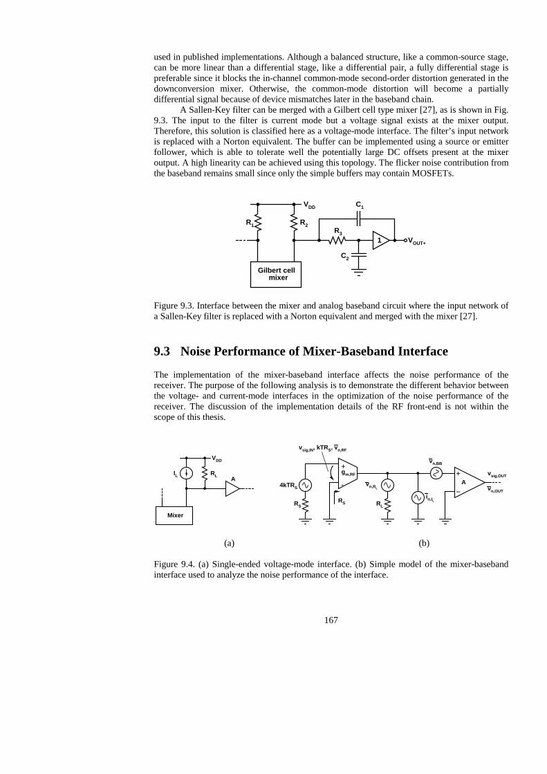
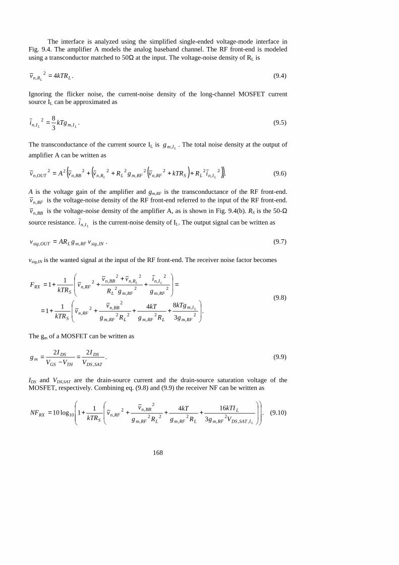
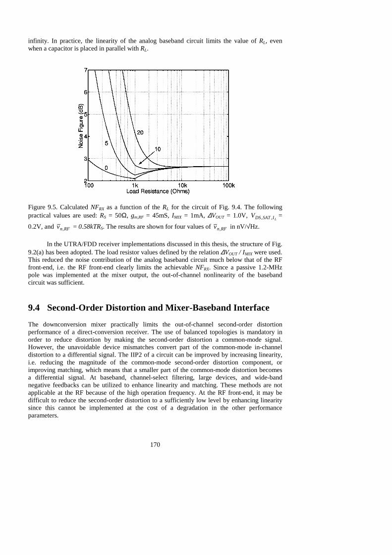
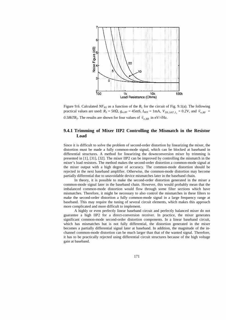
9.3 Noise Performance of Mixer-Baseband Interface ...................................................... 167 9.4 Second-Order Distortion and Mixer-Baseband Interface ........................................... 170
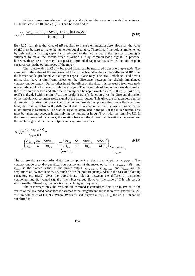
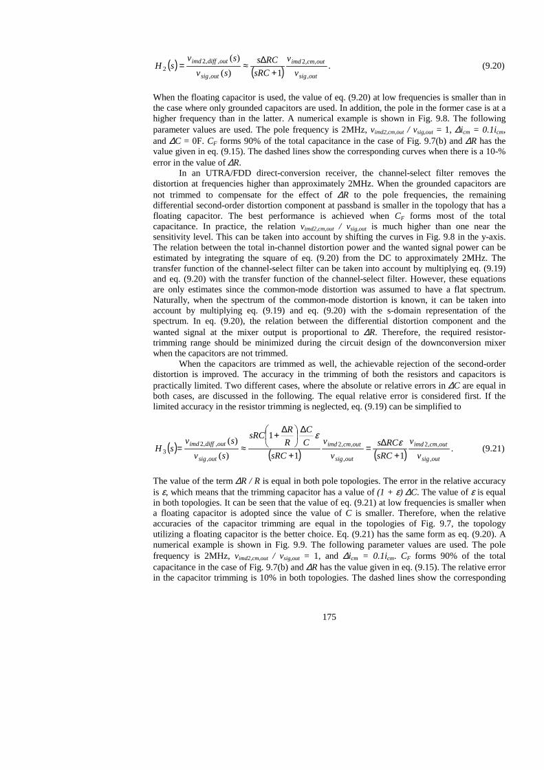
9.4.1 Trimming of Mixer IIP2 Controlling the Mismatch in the Resistor Load....... 171 9.4.2 Trimming of Mixer IIP2 Controlling the Mismatch in the Output Pole.......... 172
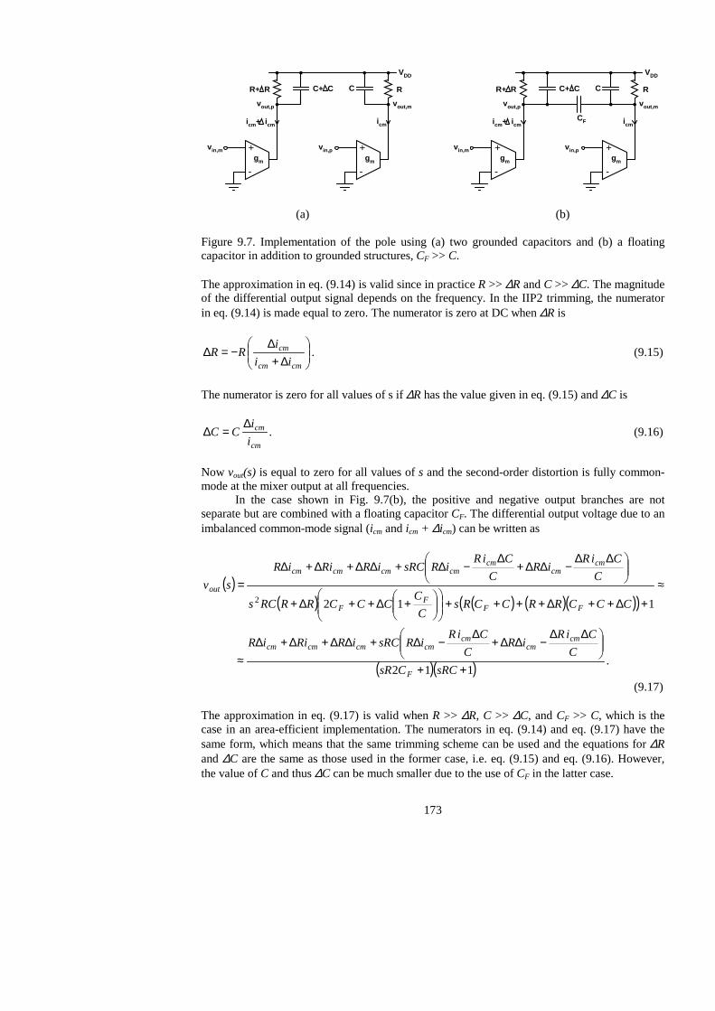
9.5 Specification of Common-Mode-to-Differential Conversion after Mixer .................. 179 9.6 Design Philosophies Enabling High IIP2 at Baseband............................................... 180 9.7 Application Case I: Multi-Band Analog Baseband Circuit for UTRA/FDD Direct-Conversion Receiver ....................................................................................... 180
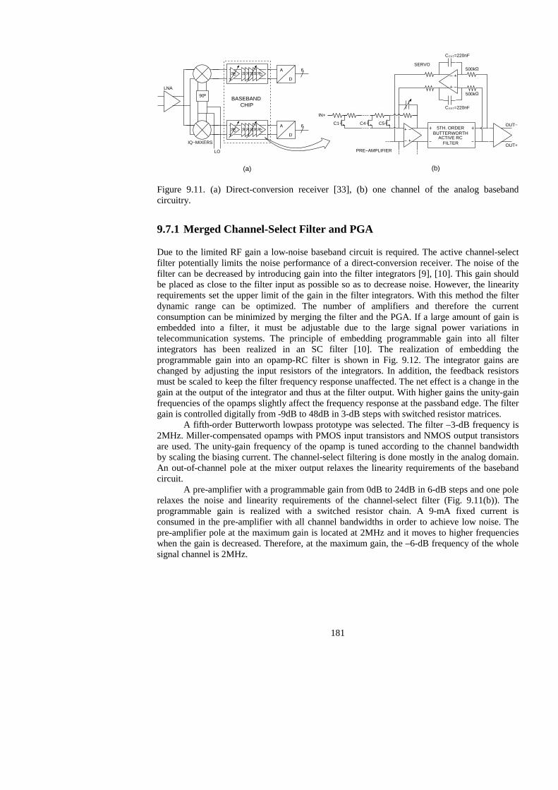
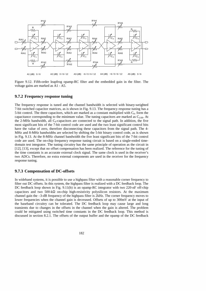
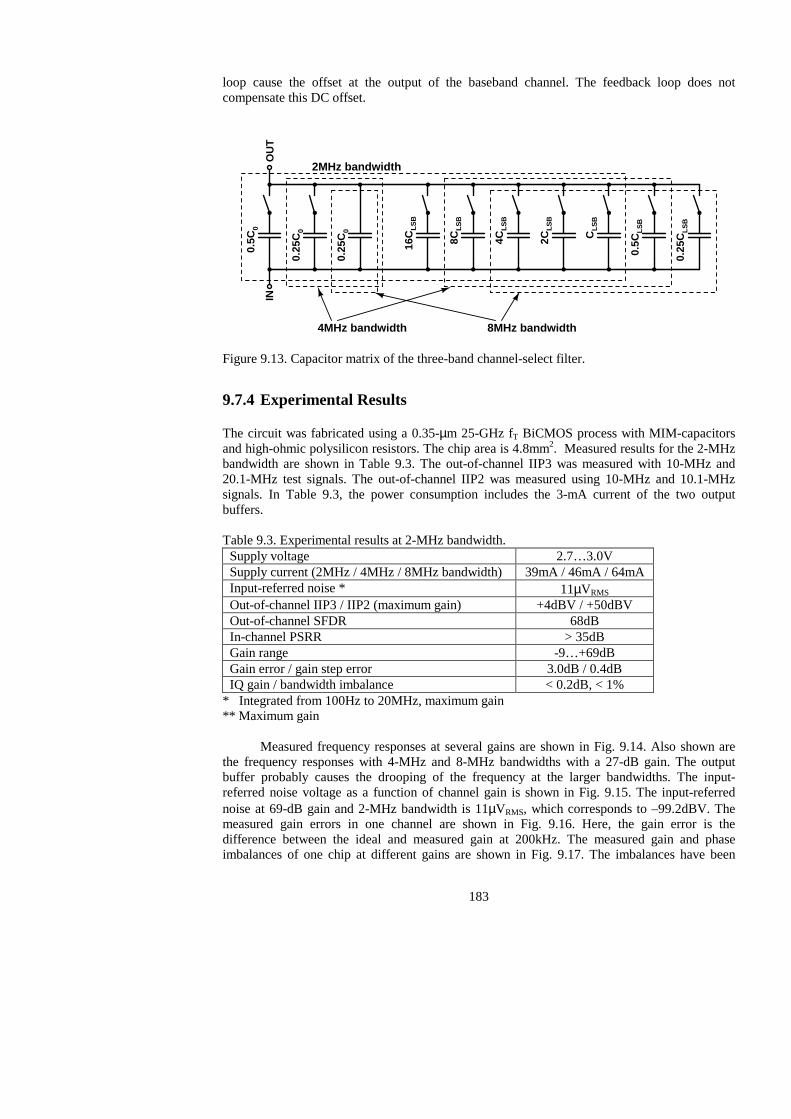
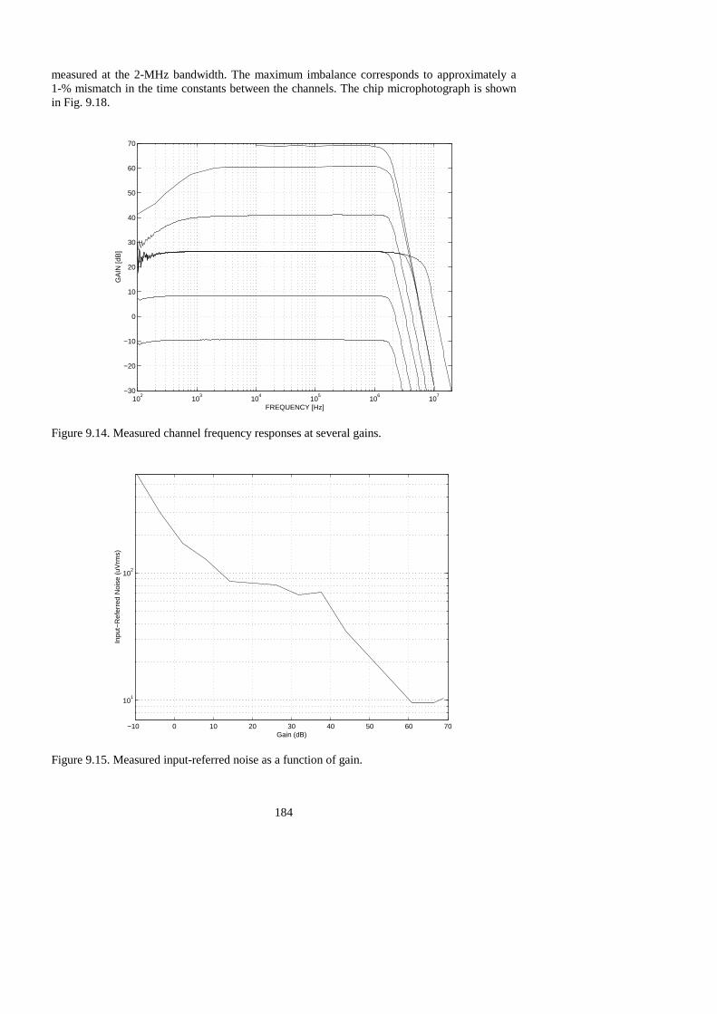
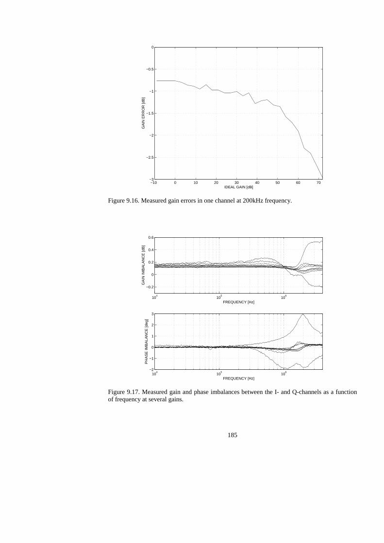
9.7.1 Merged Channel-Select Filter and PGA.......................................................... 181 9.7.2 Frequency response tuning.............................................................................. 182 9.7.3 Compensation of DC-offsets ........................................................................... 182 9.7.4 Experimental Results ...................................................................................... 183
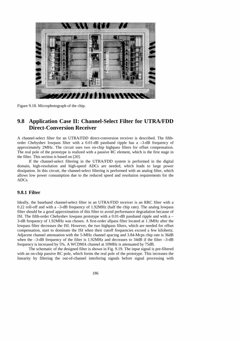
9.8 Application Case II: Channel-Select Filter for UTRA/FDD Direct-Conversion Receiver ..................................................................................................................... 186
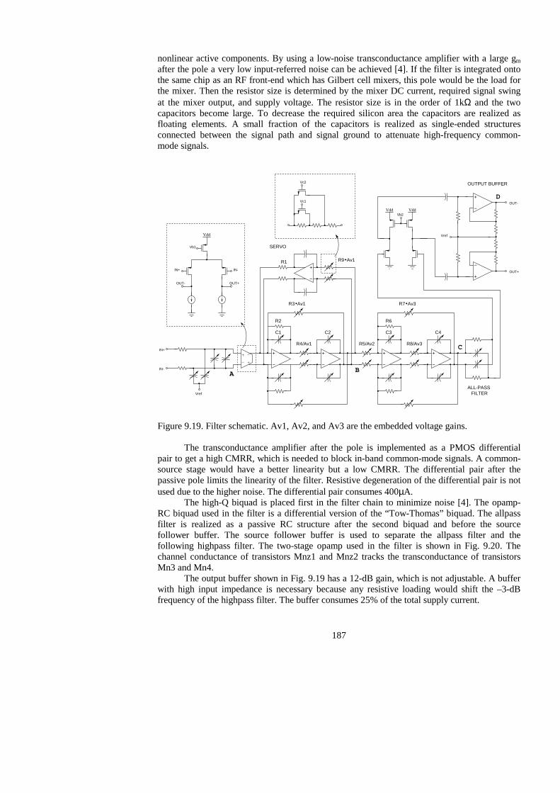
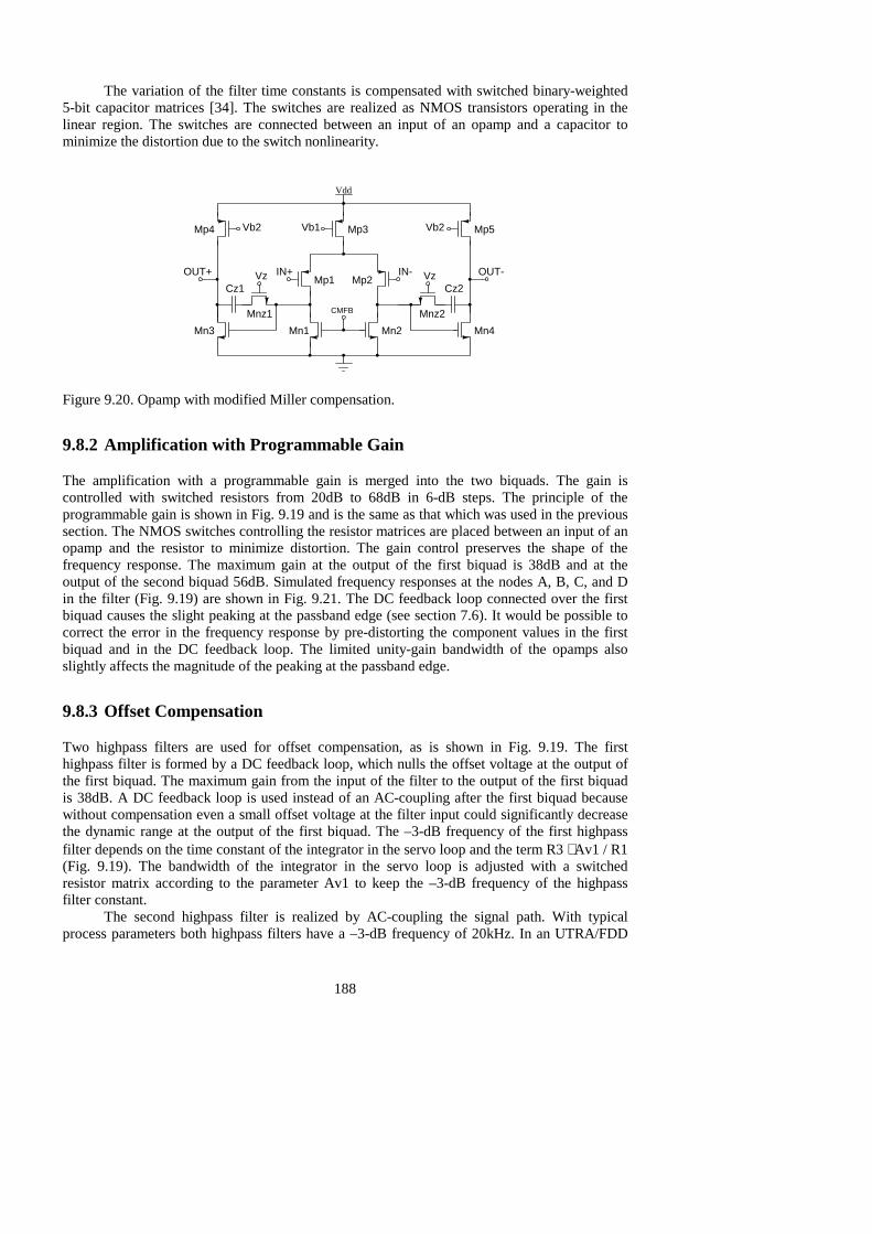
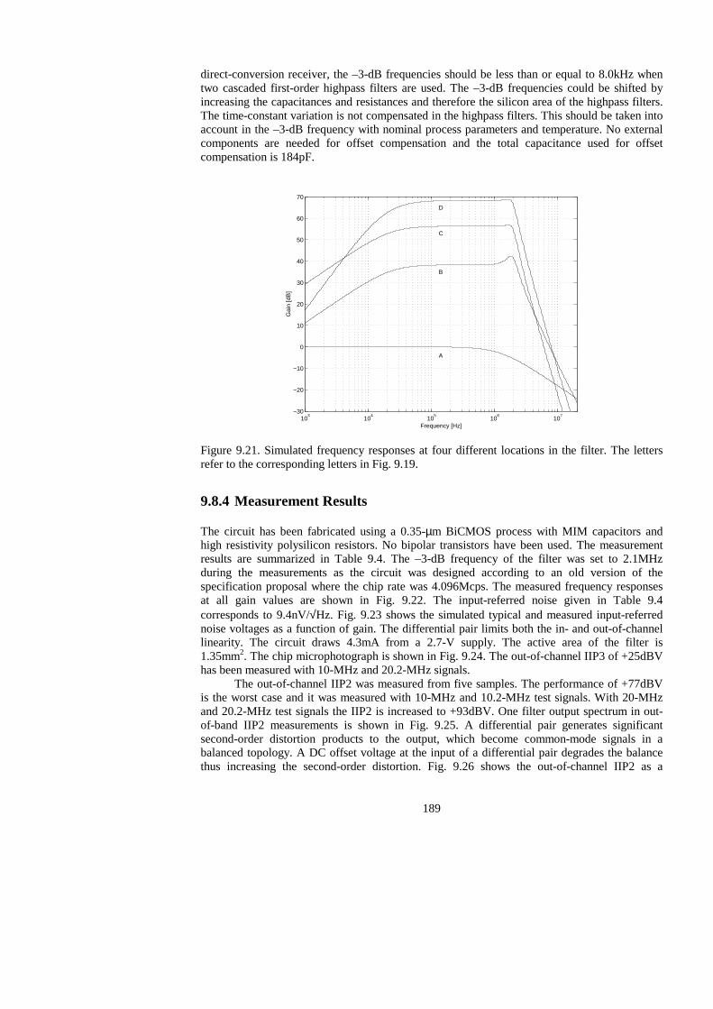
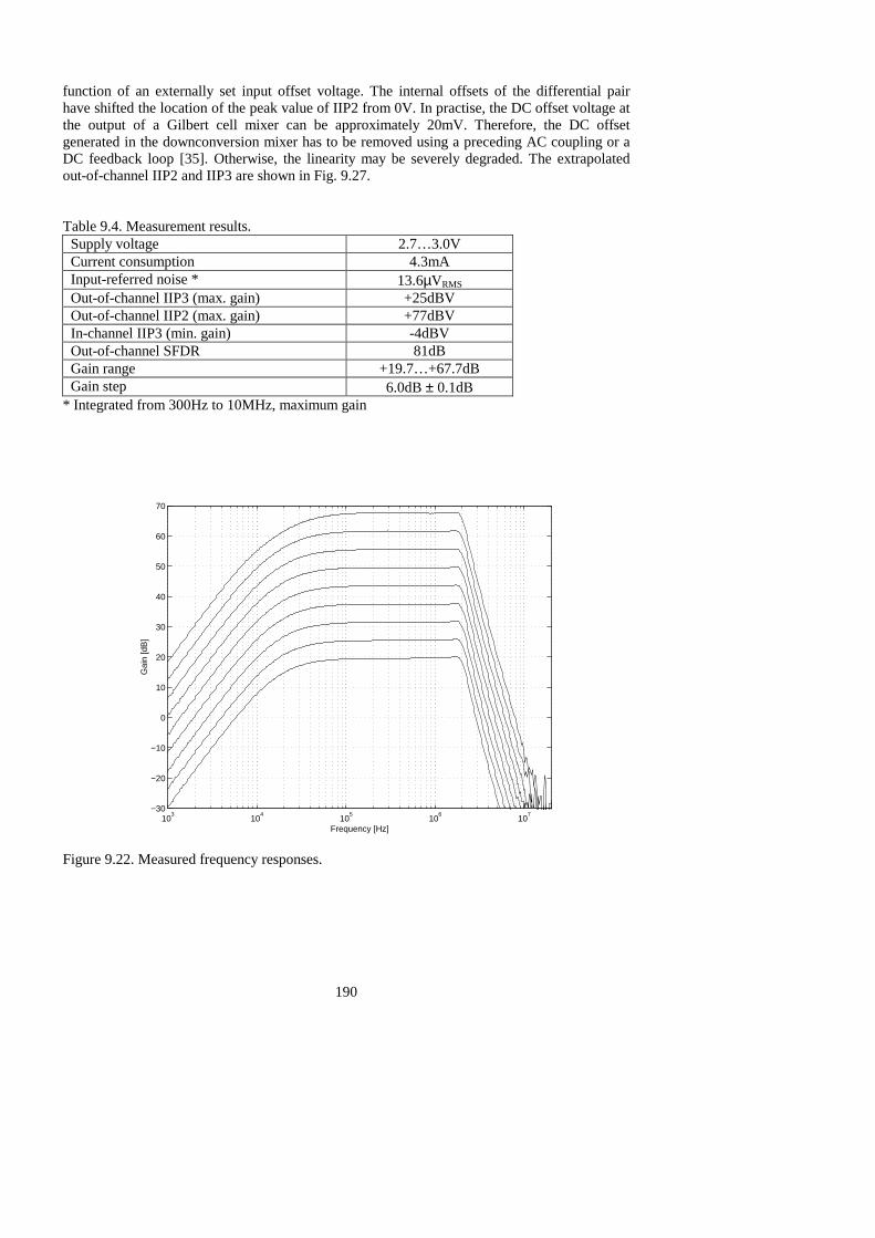
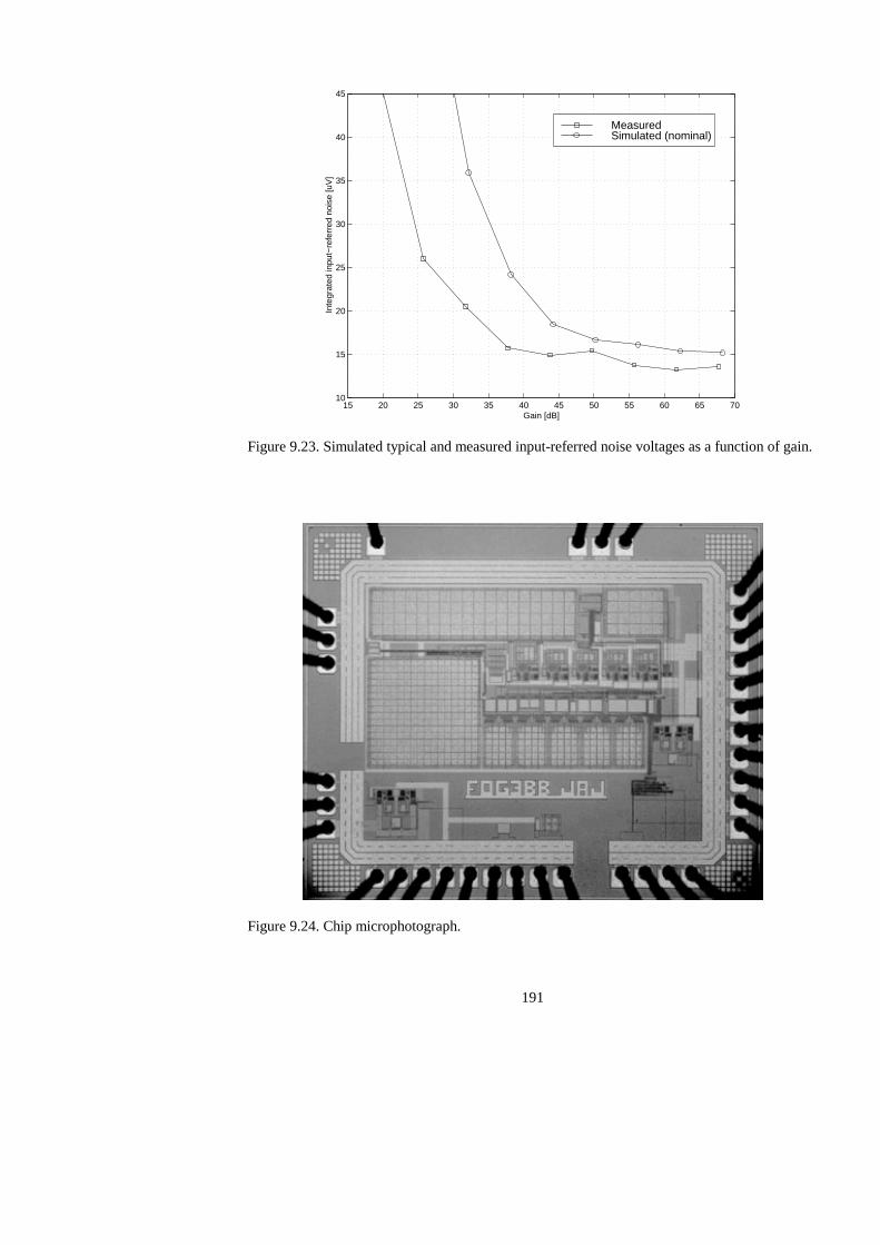
9.8.1 Filter................................................................................................................ 186 9.8.2 Amplification with Programmable Gain ......................................................... 188 9.8.3 Offset Compensation....................................................................................... 188 9.8.4 Measurement Results ...................................................................................... 189
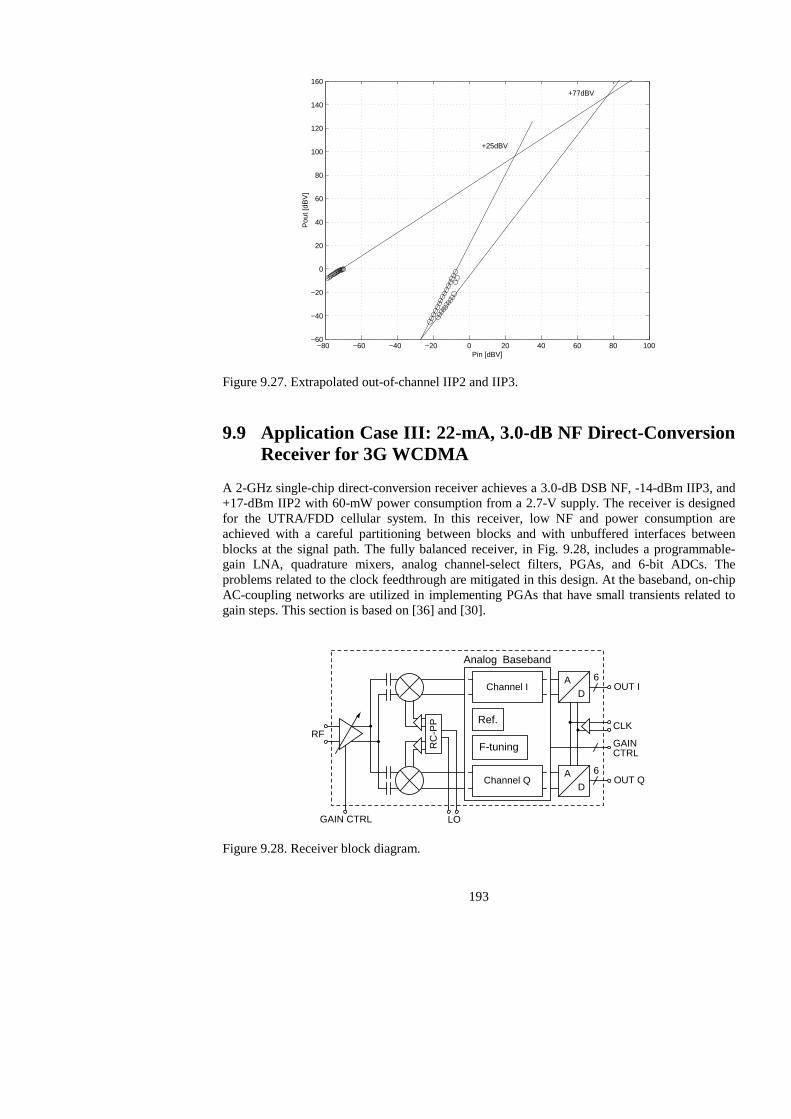
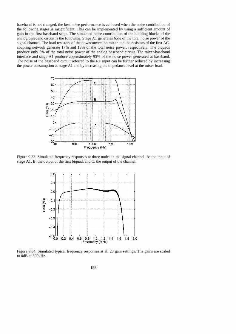
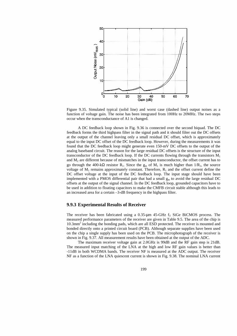
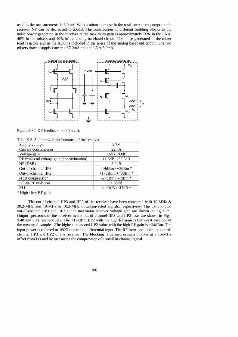
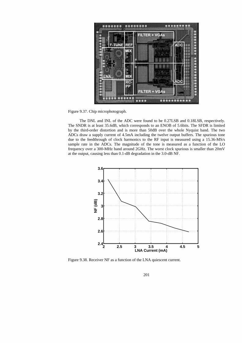
9.9 Application Case III: 22-mA, 3.0-dB NF Direct-Conversion Receiver for ............... 3G WCDMA .............................................................................................................. 193
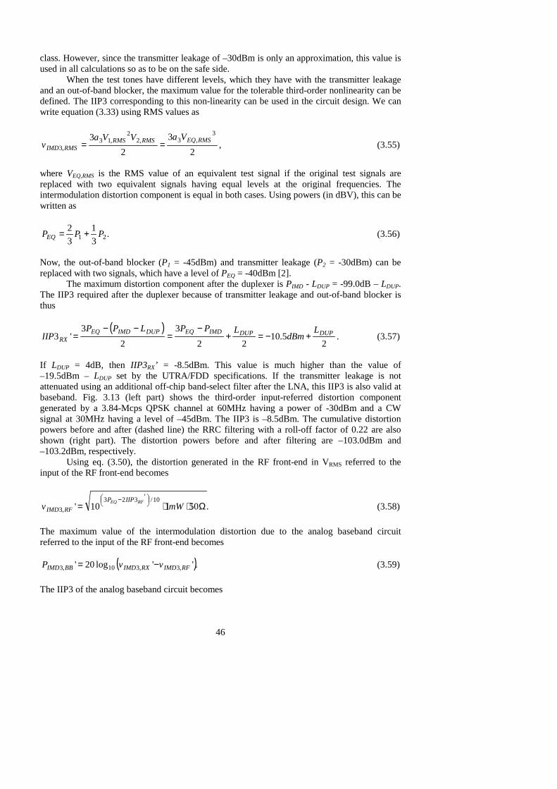
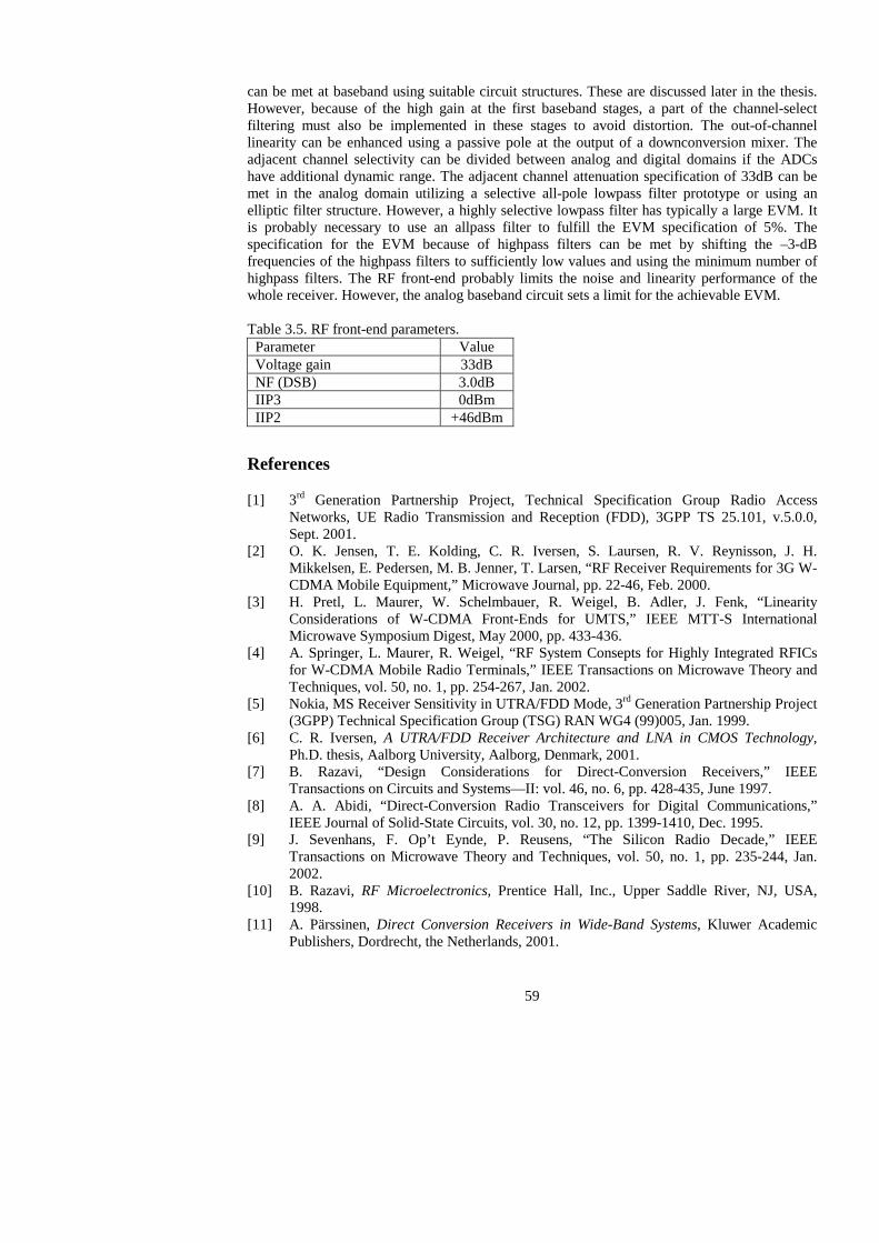
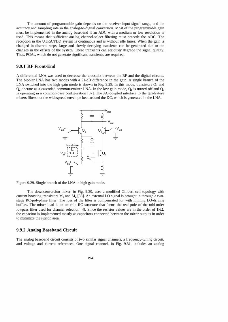
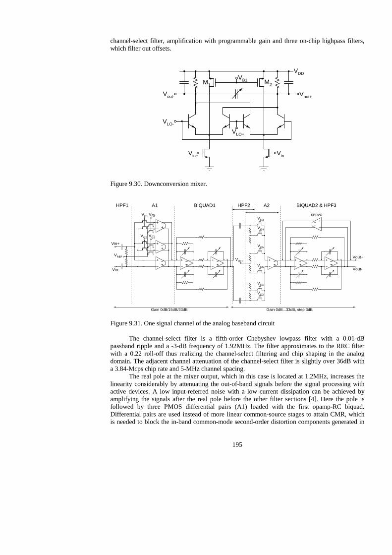
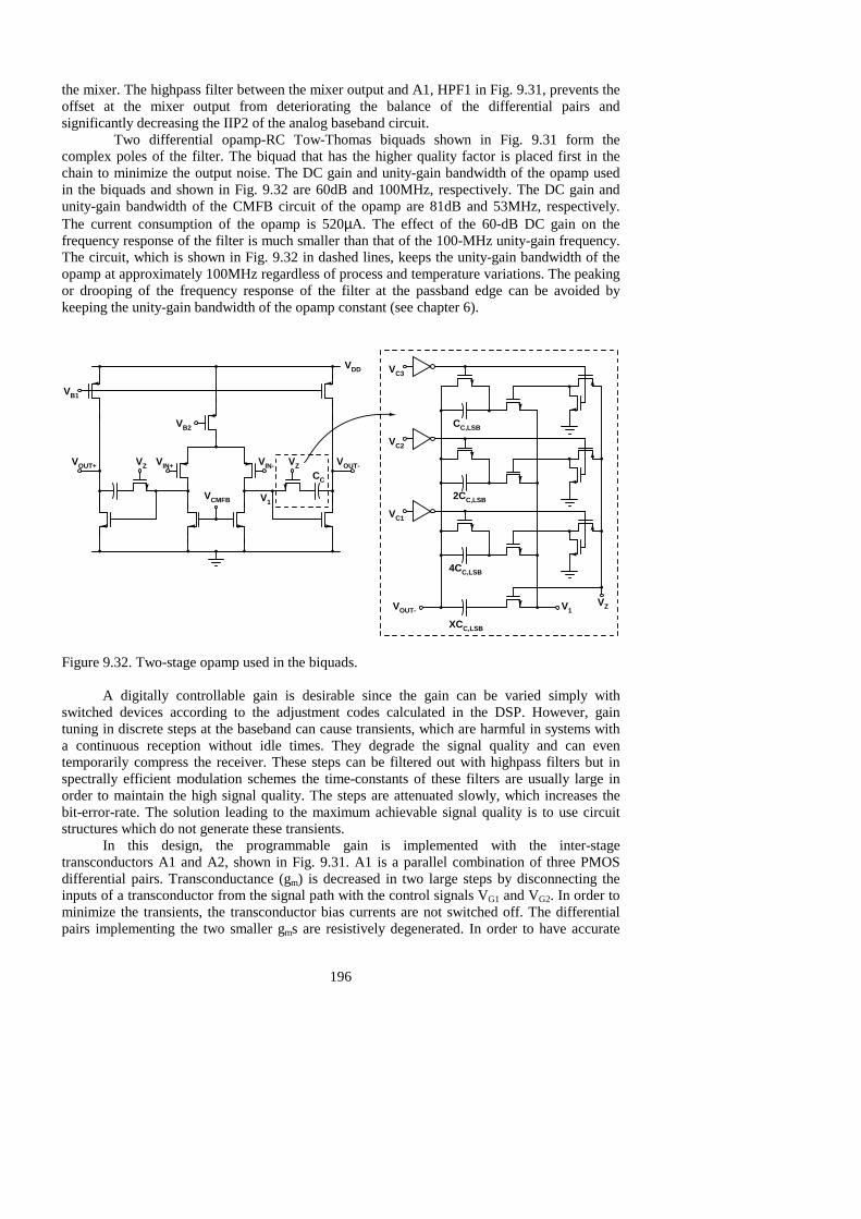
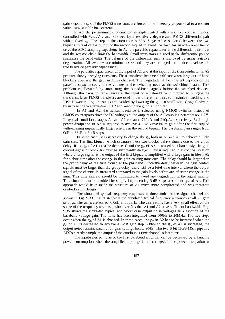
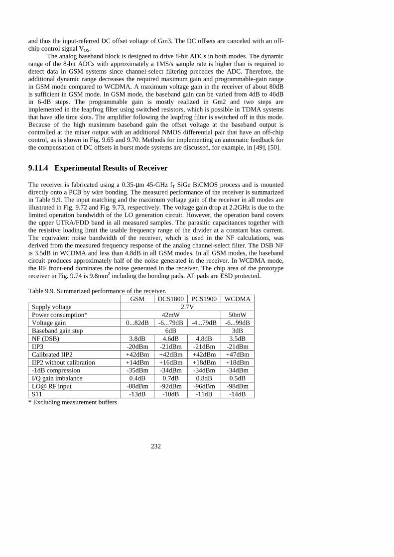
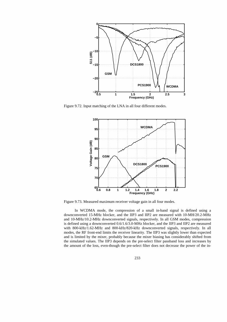
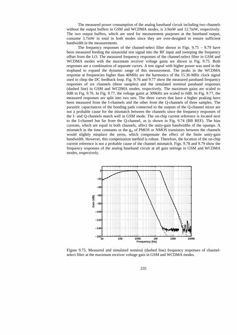
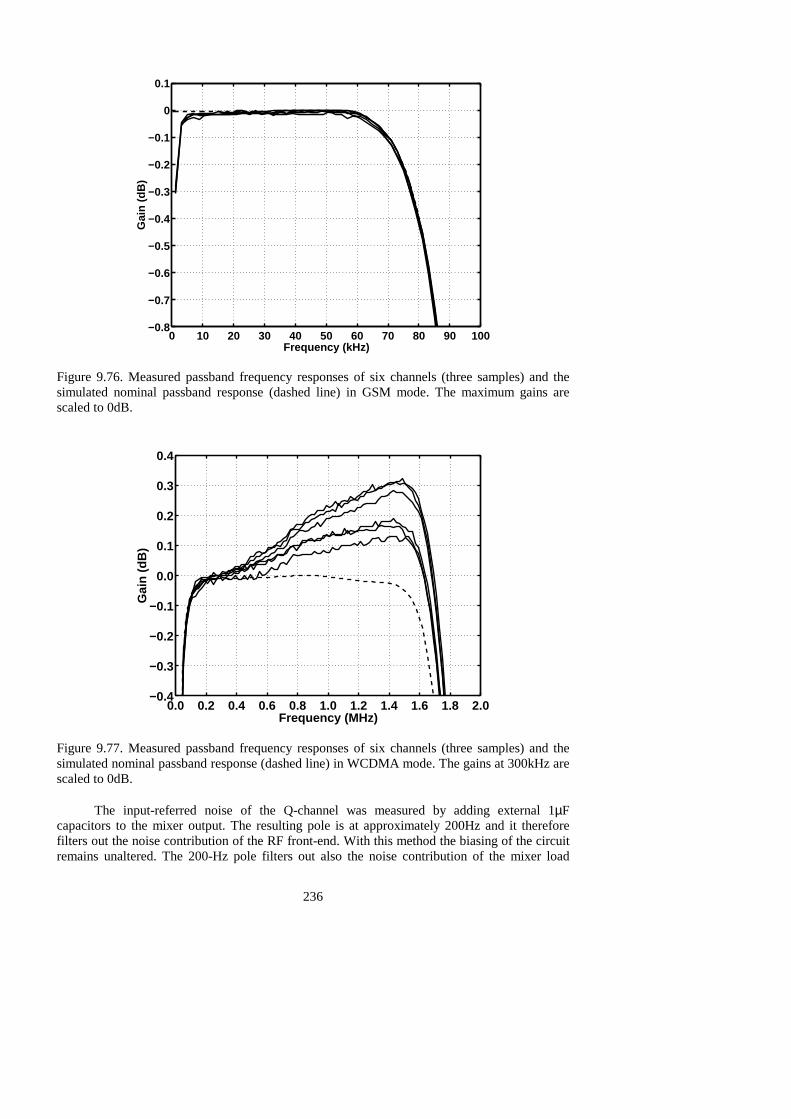
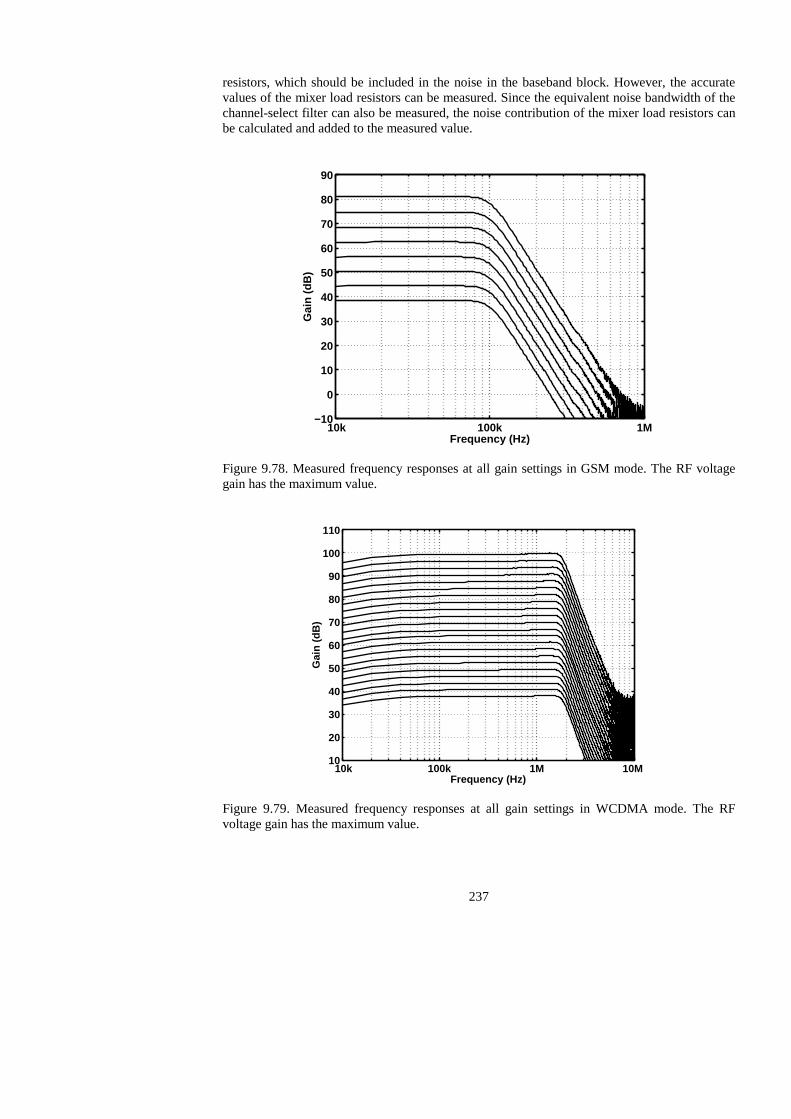
9.9.1 RF Front-End .................................................................................................. 194 9.9.2 Analog Baseband Circuit ................................................................................ 194 9.9.3 Experimental Results of Receiver ................................................................... 199 9.9.4 Experimental Results of Analog Baseband Circuit ......................................... 202
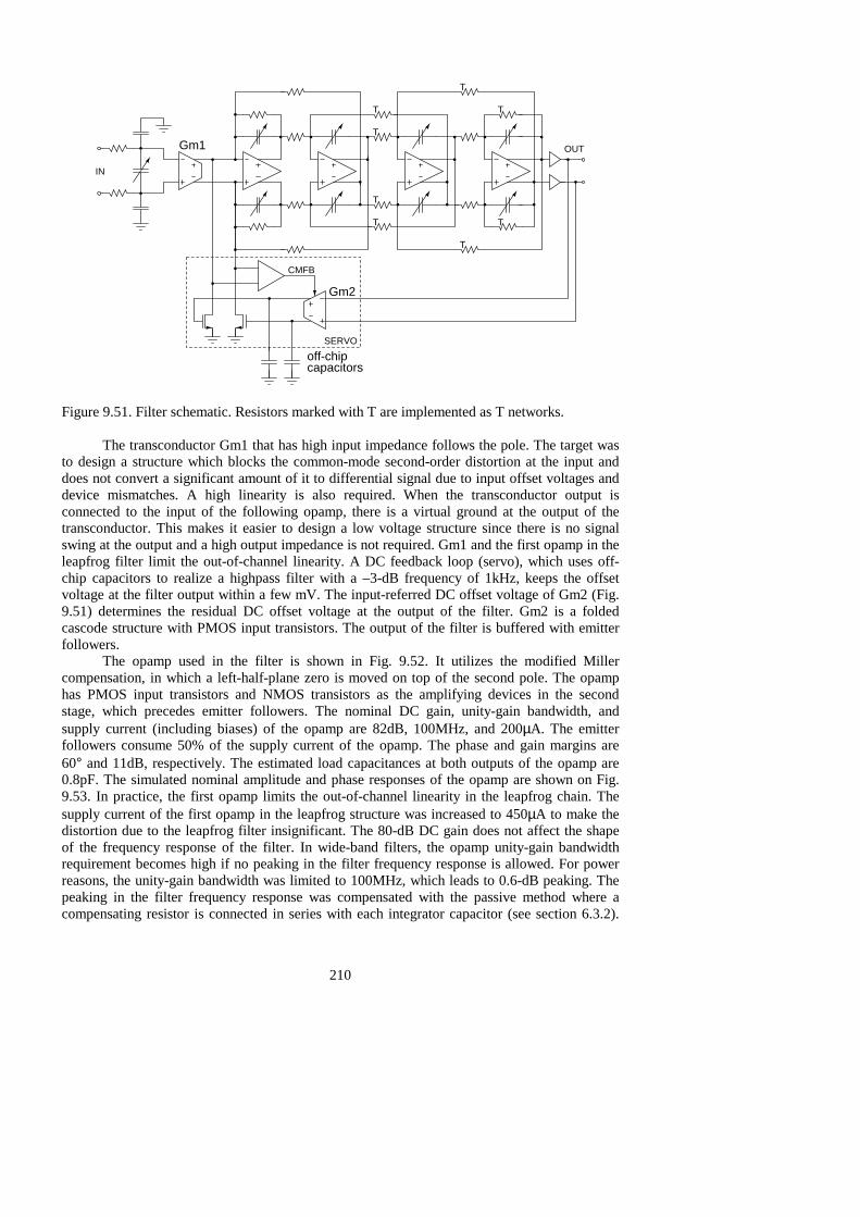
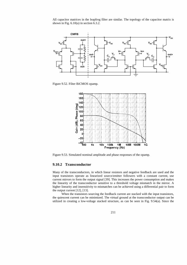
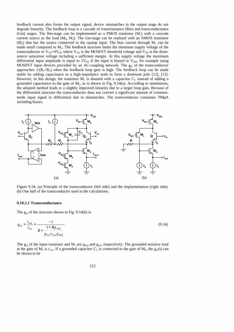
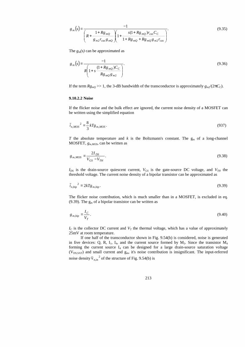
9.10 Application Case IV: UTRA/FDD Channel-Select Filter with High IIP2.................. 209 9.10.1 Filter................................................................................................................ 209 9.10.2 Transconductor ............................................................................................... 211
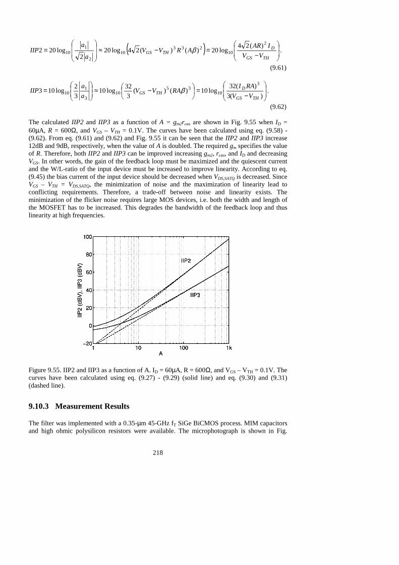
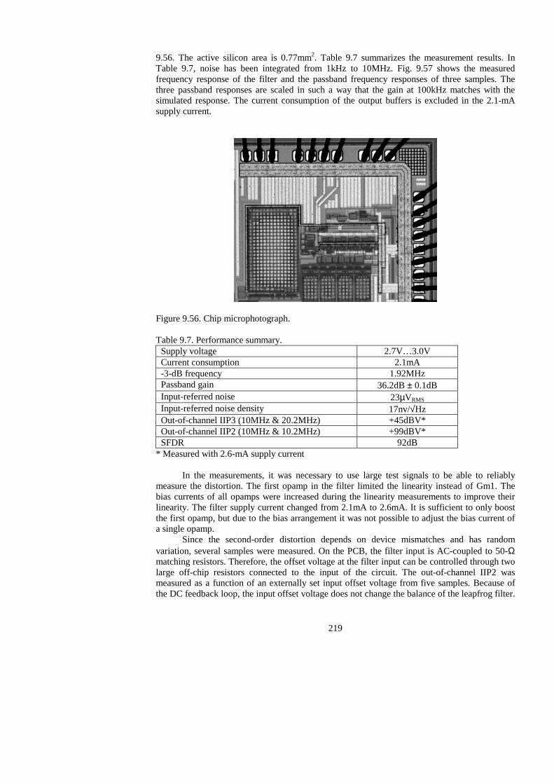
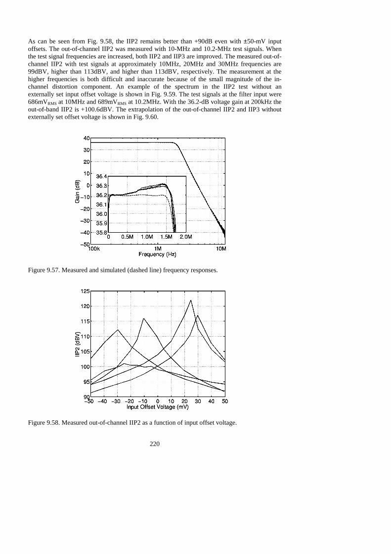
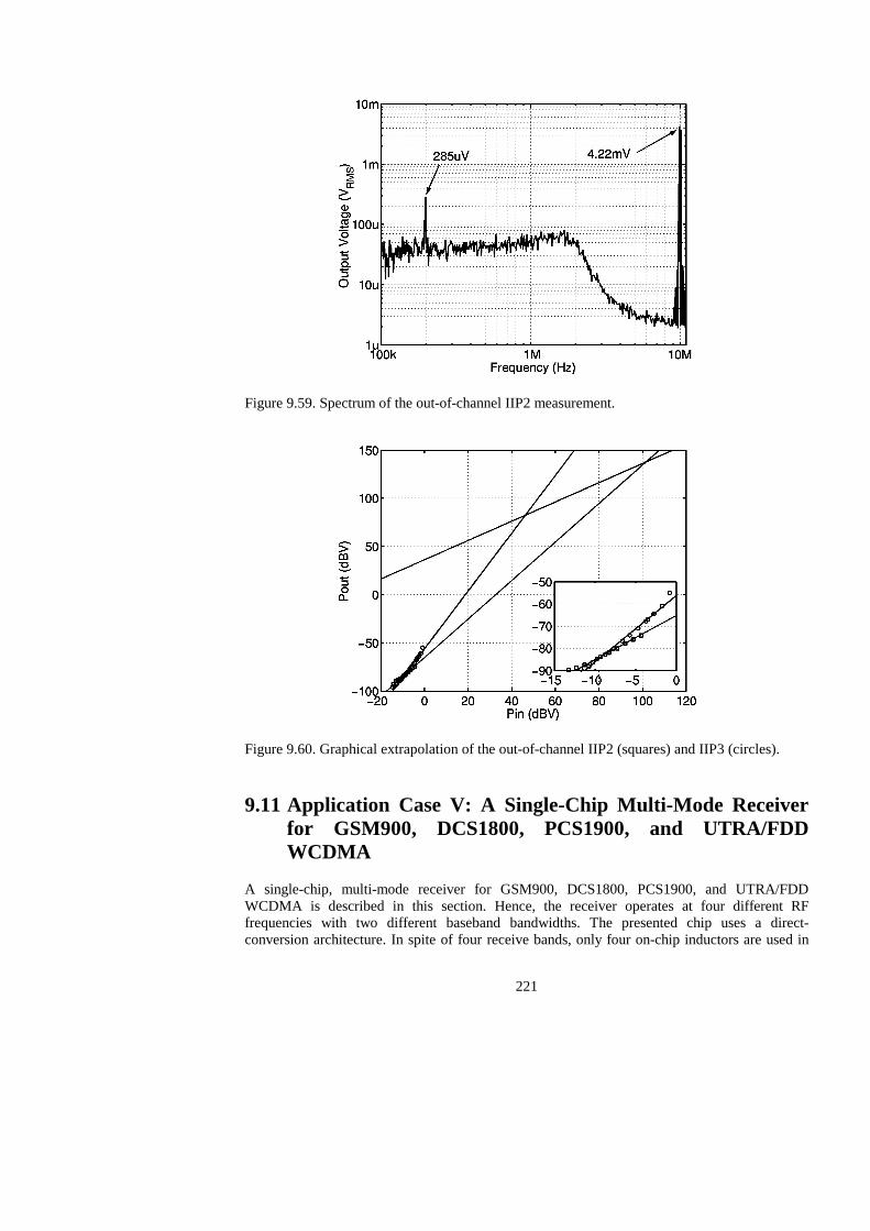
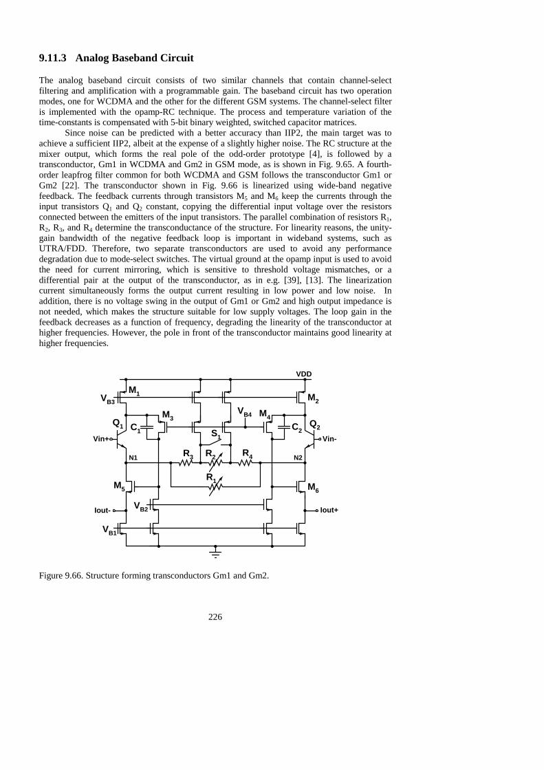
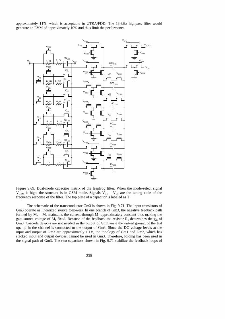
9.10.3 Measurement Results ...................................................................................... 218 9.11 Application Case V: A Single-Chip Multi-Mode Receiver for GSM900, DCS1800, PCS1900, and UTRA/FDD WCDMA...................................................... 221
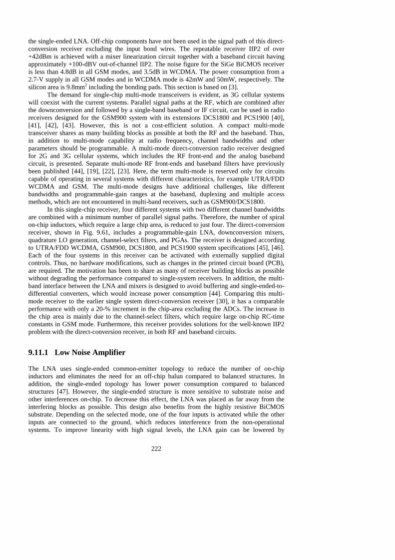
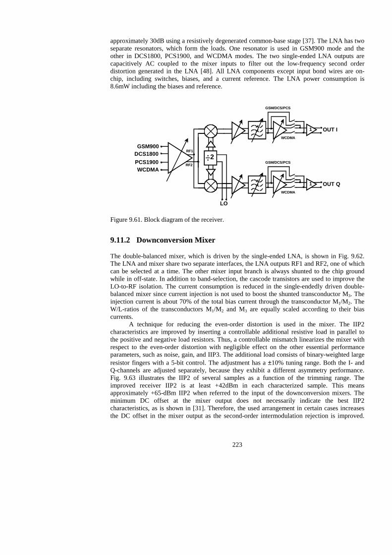
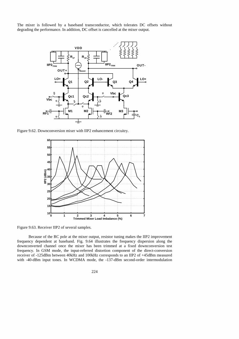
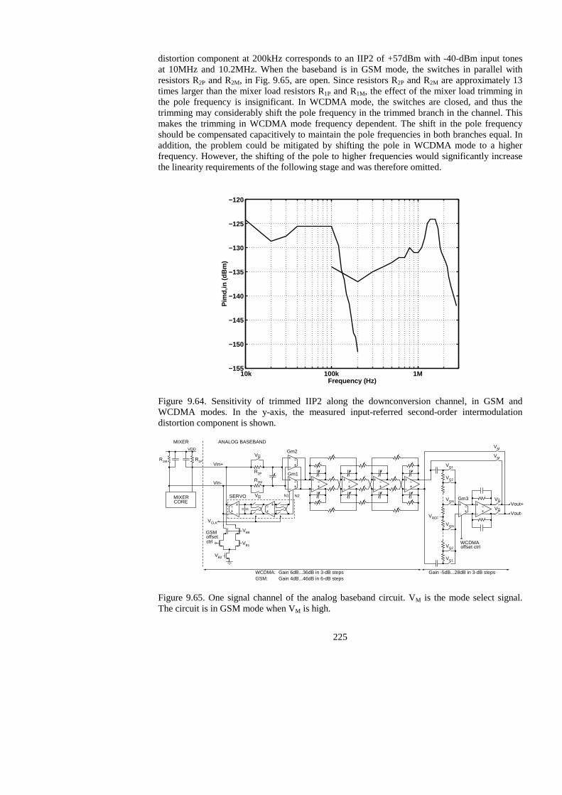
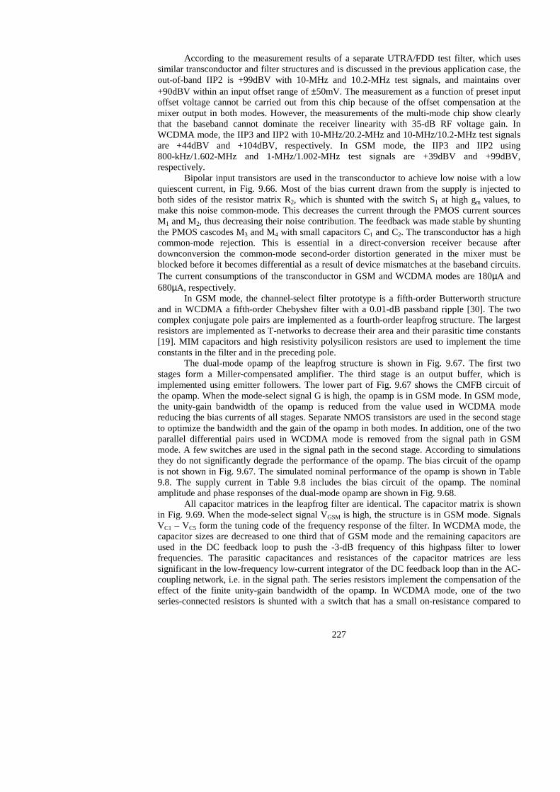
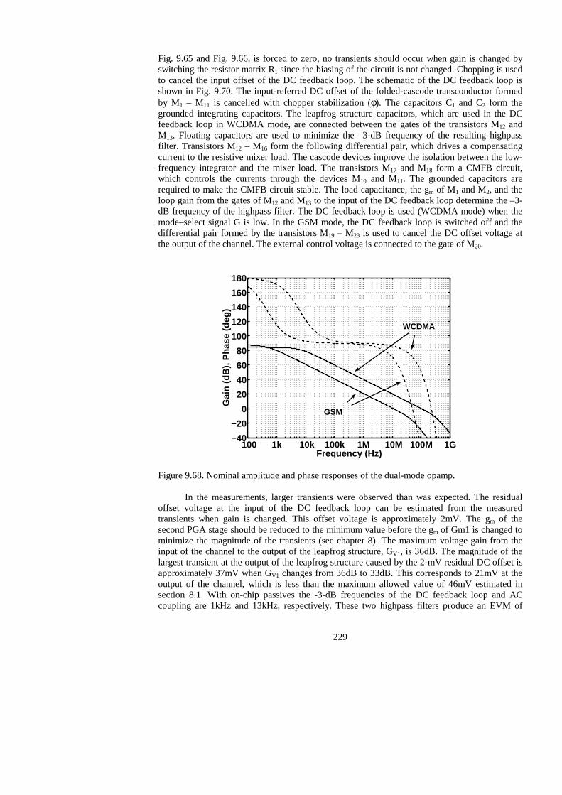
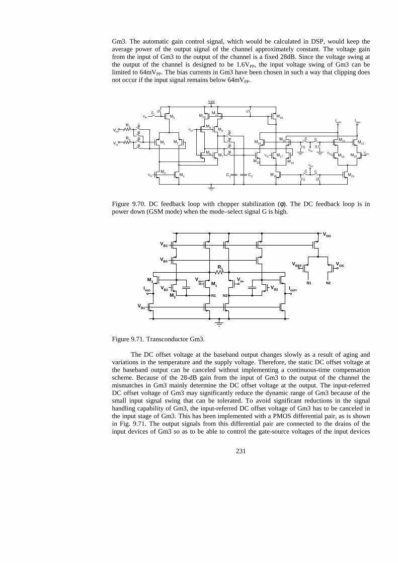
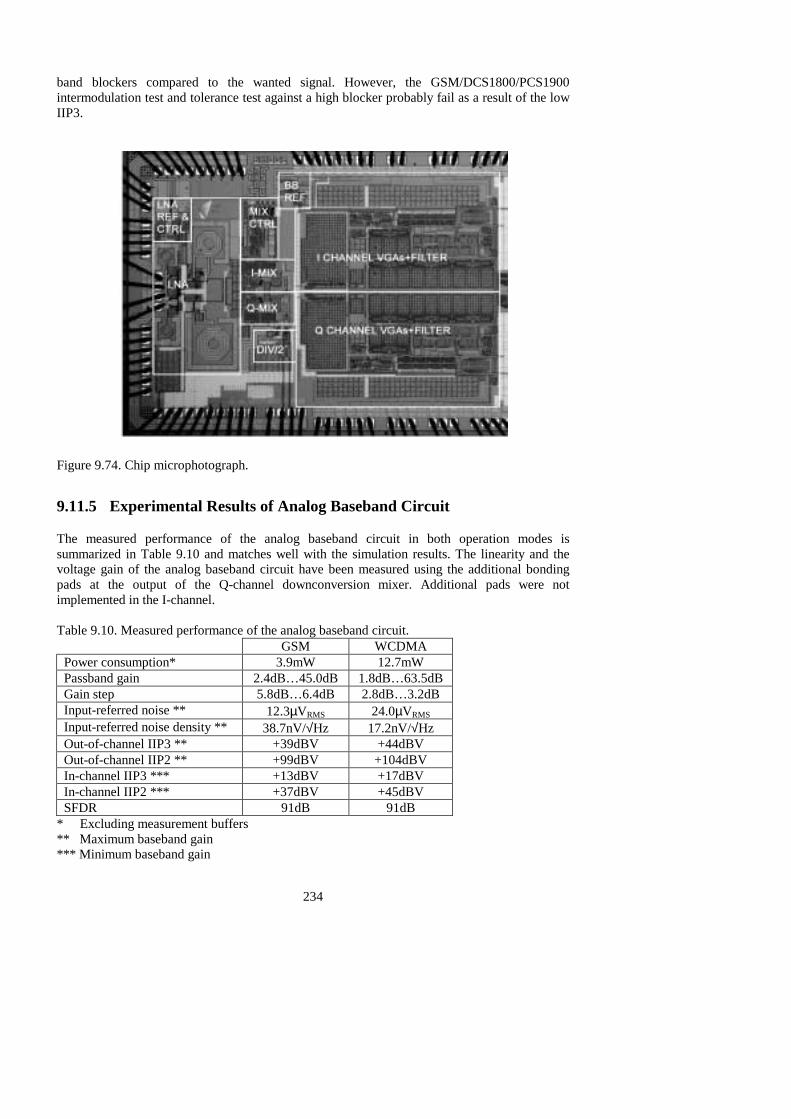
9.11.1 Low Noise Amplifier ...................................................................................... 222 9.11.2 Downconversion Mixer................................................................................... 223 9.11.3 Analog Baseband Circuit ................................................................................ 226 9.11.4 Experimental Results of Receiver ................................................................... 232 9.11.5 Experimental Results of Analog Baseband Circuit ......................................... 234
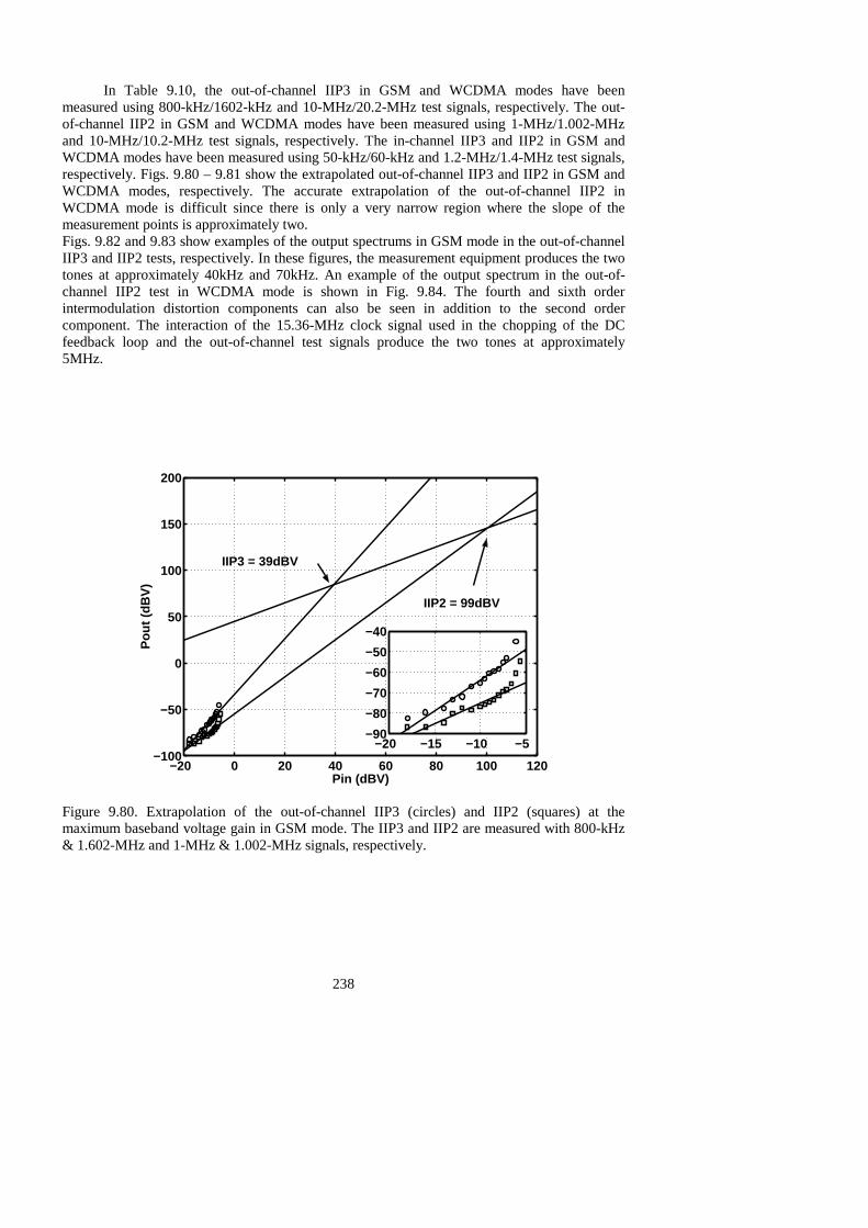
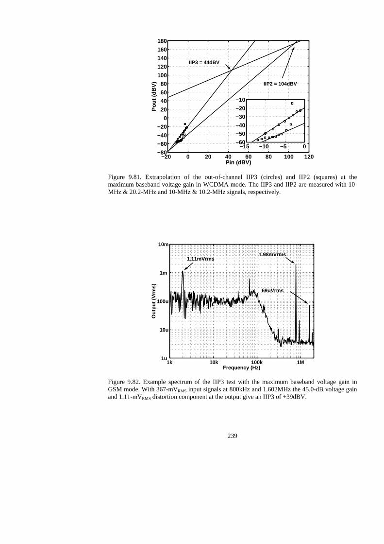
9.12 Conclusions of Application Cases I - V ..................................................................... 241 10 Conclusions........................................................................................................................ 246
1
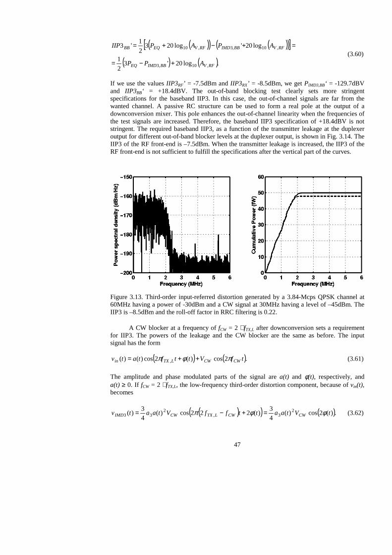
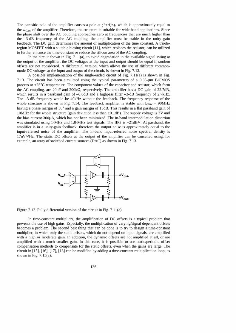
1 Introduction
1.1 Motivation
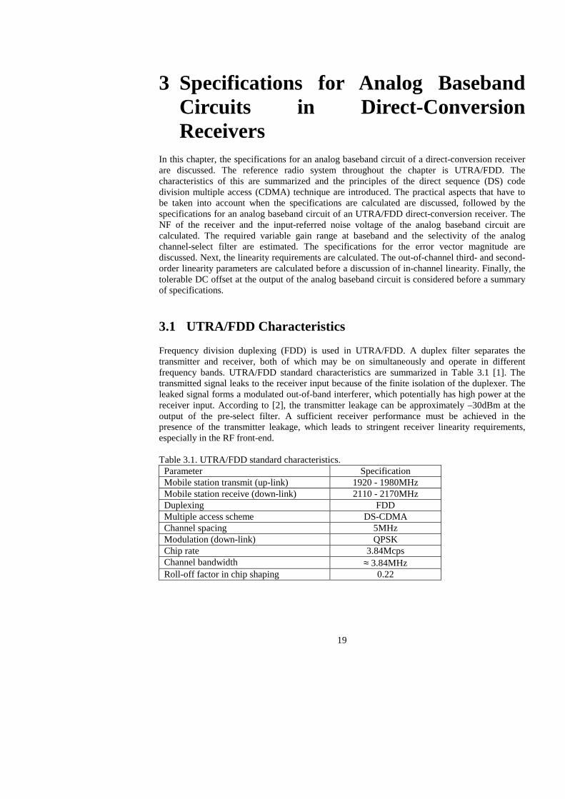
Second-generation cellular systems have utilized quite narrow signal bandwidths, while RF and IF circuits have dominated the power consumption of the analog part of the receiver. In third-generation systems, like UTRA/FDD WCDMA, the signal bandwidth at baseband is approximately 2MHz. This is much higher than in the second-generation systems. For example, in GSM, the bandwidth is over an order of magnitude narrower. It is evident that the baseband signal processing in a radio receiver will consume more power in the third-generation systems. The significance of optimizing the analog and digital baseband signal processing of a mobile phone will therefore increase in the future. The market for mobile telecommunications products has grown rapidly during the last decade. Cellular phones have become mass-produced products in a market in which price is an important factor affecting the success of the product. Price, size, talk, and stand-by times are the most important technical valuation criteria of a mobile phone. Although the analog receiver front-end does not limit the size of a mobile phone, the implementation of the receiver affects the size, battery life, cost, and manufacturability of the product. A lower cost and size can be achieved by increasing the integration level. There is a trend toward single-chip transceivers, in which all active circuitry is integrated into a single chip. Despite the recent rapid progress in the area, some off-chip passive components will remain a necessity in the near future, like antenna and RF pre-select filter. The choice of receiver architecture affects receiver performance, including sensitivity, selectivity, and power consumption. The superheterodyne architecture has been the dominating radio architecture because it offers the highest sensitivity and selectivity. The good performance is achieved by utilizing off-chip, passive RF image-reject and IF channel-select filters having high dynamic range and selectivity. At the moment, filters having comparable performance cannot be integrated. These off-chip filters are bulky and expensive. Other receiver architectures that offer higher integration levels have recently been researched extensively. Direct/conversion architecture is a promising candidate. In this architecture, the channel-select filtering can be performed on-chip and there is no need to use an image-reject filter before downconversion. It offers the highest integration level available. However, the fundamental problems of the architecture prevented its use in mobile phones until the early 90’s. Because of these problems, some building blocks, especially down-conversion mixers and analog baseband circuit, have stringent specifications that are difficult to meet. The second- and third-generation cellular systems will co-exist for some time after the new systems have been launched. In the beginning, the new systems will cover urban areas, while rural areas will be covered at a lower pace. The same handset should be able to operate in both the second- and third-generation systems. The different systems can also be used for different purposes. The need for multi-mode radio receivers operating both in the second- and third-generation systems is evident. Power consumption is of special importance in cellular phones, since power consumption and maximum battery charge determine stand-by and active times. The supply voltage of digital CMOS circuits is decreasing to minimize the power consumption per logic cell. In addition, the shrinking of device dimensions lowers the maximum allowed supply voltage. It is feasible to have a single supply for the whole transceiver, which means that the
2
supply voltage of analog circuits should decrease as well. However, the relation between supply voltage and power consumption is not as straightforward in the analog domain as in the digital. A low supply voltage limits the amount of stacked transistors and leads to a larger number of current branches. On the other hand, the deterioration of the signal handling capability of analog circuitry is not typically allowed. Dynamic range is limited by noise and supply voltage if a sufficient linearity is assumed. In analog circuits, it becomes increasingly difficult to achieve the required performance with low power when supply voltages decrease. Because of the advances in digital CMOS circuit technology and A/D converter (ADC) implementations, the interface between analog and digital signal processing is moving closer to the antenna. Signal processing functions are moved to the digital domain where all non-idealities of the analog domain can be avoided. The ADCs have become the bottleneck in this development. When the analog-to-digital interface is moved closer to the antenna, the performance requirements of the ADCs become more and more stringent, which increases power consumption. In direct-conversion receivers, there will be a continuous-time lowpass filter at baseband. In narrowband systems, this filter can be a simple structure operating as an anti-alias structure for the following ADC or ∆Σ modulator. In low-power, wide-band receivers, probably a more complicated and higher-order filter will be required to effectively attenuate out-of-band signals and make possible a decrease in the required sample rate and dynamic range in the analog-to-digital conversion and clock frequency in the digital back-end. In low-power, wide-band direct-conversion receivers, particular signal processing functions will remain in the analog domain for reasons relating to power consumption.
1.2 Research Contribution and Publications
This thesis concentrates on the analog baseband signal processing in direct-conversion receivers targeted for the third-generation cellular system UTRA/FDD. The system characteristics and requirements for radio receivers in wireless communications systems, like multiple access methods, duplexing, modulation, and radio-channel characteristics, are not introduced here. The design parameters for a direct-conversion receiver and analog baseband circuit are explained, starting with the UTRA/FDD specifications for a mobile station radio receiver. The target of the research has been to design and implement an analog baseband circuit for an UTRA/FDD direct-conversion receiver that would meet the essential specified requirements. The author has found solutions to the problems of the direct-conversion receiver that are related to baseband circuits. These include the requirement for a high dynamic range and very low second-order distortion with low power consumption. Since the first stages of the analog baseband circuit mostly determine the dynamic range and amount of second-order distortion, the research has focused on these issues. Effort has been put into optimizing the architecture of the analog baseband signal channel. In addition to this, on-chip solutions have been proposed for offset removal. In systems that have continuous reception without idle time slots, such as UTRA/FDD, unavoidable baseband offsets may cause transients when baseband gain is changed in discrete steps. The author has proposed solutions to mitigate these transients. A huge number of active analog lowpass filters have been reported in the literature. It is not the purpose of this thesis to review the development of these filters comprehensively. Active analog filter techniques and their characteristics are introduced and compared from the viewpoint of their suitability for wide-band direct-conversion receivers. The focus is on recently published designs. All IC implementations presented in this thesis are targeted for UTRA/FDD applications. In the latest receiver IC, GSM900, DCS1800, and PCS1900 cellular systems are also included. BiCMOS technology, including high-quality capacitors and resistors, has been used in all these ICs. The research team, which designed, implemented, and measured the receivers presented in this thesis, consisted of five members including the author. The other
3
researchers were Dr. Kalle Kivekäs, Dr. Aarno Pärssinen, Mr. Jussi Ryynänen, and Dr. Lauri Sumanen. In each paper, the first author had the main responsibility for the manuscript. Conference article P1 describes a chip-set direct-conversion receiver designed for UTRA/FDD. The author contributed to system simulations with the aid of Dr. Aarno Pärssinen and designed and implemented the analog baseband circuit. Mr. Ryynänen and Dr. Pärssinen implemented the RF front-end, while Dr. Sumanen implemented the ADCs. Paper P2 presents the first IC that the author implemented in this research project. It is the analog baseband circuit for the chip-set direct-conversion receiver of publication P1. The channel-select filter merges filtering and amplification with a programmable gain to improve dynamic range. The author developed the merging principle and designed, implemented, and measured the IC. The design of a 1.5-V opamp-RC lowpass filter is discussed in publication P3. Low-voltage operation is achieved using current sources as level shifters. The author modified a previously published method. Low-voltage operation is achieved without an increase in the current consumption of the filter. Paper P4 is a journal article based on the conference article P1. The contribution of the author is the same as in paper P1. Publication P5 presents a single-chip version of the receiver of paper P1. Only minor circuit modifications were made. The contributions are the same as those mentioned earlier. Paper P6 describes a channel-select filter for an UTRA/FDD direct-conversion receiver. It has better performance, with lower quiescent current, than the IC described in paper P2. The architecture of the baseband signal channel, the interface with the mixers, and the filter prototype have been changed. The author designed, implemented, and tested this IC. Paper P7 presents a single-chip direct-conversion receiver designed for UTRA/FDD. The author contributed to the receiver system design and designed and implemented the analog baseband circuitry; he also participated in the receiver measurements. The transients caused by offsets when baseband gain is changed digitally in a system having continuous reception have been mitigated using suitable circuit structures. Mr. Jussi Ryynänen, Dr. Kalle Kivekäs, and Dr. Aarno Pärssinen implemented the RF front-end. Dr. Lauri Sumanen implemented the ADCs. Publication P8 is a journal paper based on conference article P7. The author’s contribution in paper P8 is the same as in paper P7. In this paper, the transients related to digitally controlled gain at baseband are discussed in more detail. Conference article P9 describes an analog channel-select filter achieving a high IIP2. The filter is designed for an UTRA/FDD direct-conversion receiver. The author designed, implemented, and measured the filter. Journal article P10 presents a single-chip, quad-mode direct-conversion receiver. The author is responsible for the design and implementation of the analog baseband circuit, which is based on the structure described in paper P9. The receiver was implemented in co-operation with Dr. Kalle Kivekäs, Dr. Aarno Pärssinen, Mr. Jussi Ryynänen, and Dr. Lauri Sumanen. Publications included in this thesis in chronological order: P1 A. Pärssinen, J. Jussila, J. Ryynänen, L. Sumanen, K. Halonen, “A Wide-band Direct
Conversion Receiver for WCDMA Applications”, IEEE International Solid-State Circuits Conference Digest of Technical Papers, Feb. 1999, pp. 220-221.
P2 J. Jussila, A. Pärssinen, K. Halonen, “An Analog Baseband Circuitry for a WCDMA Direct Conversion Receiver”, Proceedings of the European Solid-State Circuits Conference, Sept. 1999, pp. 166-169.
4
P3 J. Jussila, K. Halonen, “A 1.5V Active RC Filter for WCDMA Applications”, Proceedings of the IEEE International Conference on Electronics, Circuits and Systems, Sept. 1999, pp. I-489-492.
P4 A. Pärssinen, J. Jussila, J. Ryynänen, L. Sumanen, K. A. I. Halonen, “A 2-GHz Wide-band Direct Conversion Receiver for WCDMA Applications”, IEEE Journal of Solid-State Circuits, vol. 34, no. 12, pp.1893-1903, Dec. 1999.
P5 A. Pärssinen, J. Jussila, J. Ryynänen, L. Sumanen, K. Kivekäs, K. Halonen, “A Wide-Band Direct Conversion Receiver with On-Chip A/D Converters”, IEEE Symposium on VLSI Circuits Digest of Technical Papers, June 2000, pp. 32-33.
P6 J. Jussila, A. Pärssinen, K. Halonen, “A Channel Selection Filter for a WCDMA Direct Conversion Receiver”, Proceedings of the European Solid-State Circuits Conference, Sept. 2000, pp. 236-239.
P7 J. Jussila, J. Ryynänen, K. Kivekäs, L. Sumanen, A. Pärssinen, K. Halonen, “A 22mA 3.7dB NF Direct Conversion Receiver for 3G WCDMA,” IEEE International Solid-State Circuits Conference Digest of Technical Papers, Feb. 2001, pp. 284-285.
P8 J. Jussila, J. Ryynänen, K. Kivekäs, L. Sumanen, A. Pärssinen, K. Halonen, “A 22-mA 3.0-dB NF Direct Conversion Receiver for 3G WCDMA,” IEEE Journal of Solid-State-Circuits, vol. 36, no. 12, pp. 2025-2029, Dec. 2001.
P9 J. Jussila, K. Halonen, “WCDMA Channel Selection Filter with High IIP2,” Proceedings of the IEEE International Symposium on Circuit and Systems, May 2002, pp. I-533-536.
P10 J. Ryynänen, K. Kivekäs, J. Jussila, L. Sumanen, A. Pärssinen, K. Halonen, “A Single-Chip Multimode Receiver for GSM900, DCS1800, PCS1900, and WCDMA,” IEEE Journal of Solid-State Circuits, vol. 38, no. 4, pp. 594-602, Apr. 2003.
Other publications related to the topic: P11 J. Ryynänen, A. Pärssinen, J. Jussila, K. Halonen, “An RF Front-End for the Direct
Conversion WCDMA Receiver”, IEEE Radio Frequency Integrated Circuits Symposium Digest of Papers, May 1999, pp. 21-24.
P12 J. Ryynänen, K. Kivekäs, J. Jussila, A. Pärssinen, K. Halonen, “A Dual-Band RF Front-End for WCDMA and GSM Applications,” Proceedings of the IEEE Custom Integrated Circuits Conference, May 2000, pp. 175-178.
P13 A. Pärssinen, J. Jussila, J. Ryynänen, L. Sumanen, K. Kivekäs, K. Halonen, “Circuit Solutions for WCDMA Direct Conversion Receiver”, Proceedings of the NORSIG Conference, June 2000, pp. 1-4.
P14 T. Hollman, S. Lindfors, M. Länsirinne, J. Jussila, K. Halonen, “A 2.7V CMOS Dual-Mode Baseband Filter for PDC and WCDMA,” Proceedings of the European Solid-State Circuits Conference, Sept. 2000, pp 176-179.
P15 K. Kivekäs, A. Pärssinen, J. Jussila, J. Ryynänen, K. Halonen, “Design of Low-Voltage Active Mixer for Direct Conversion Receivers,” Proceedings of the IEEE International Symposium on Circuit and Systems, May 2001, pp. IV-382-385.
P16 T. Hollman, S. Lindfors, M. Länsirinne, J. Jussila, K. Halonen, “A 2.7-V CMOS Dual-Mode Baseband Filter for PDC and WCDMA,” IEEE Journal of Solid-State Circuits, vol. 36, no. 7, pp. 1148-1153, July 2001.
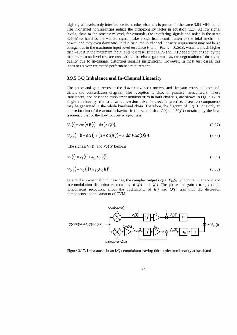
P17 J. Ryynänen, K. Kivekäs, J. Jussila, A. Pärssinen, K. Halonen, “A Dual-Band RF Front-End for WCDMA and GSM Applications,” IEEE Journal of Solid-State-Circuits, vol. 36, no. 8, pp. 1198-1204, Aug. 2001.
P18 J. Ryynänen, K. Kivekäs, J. Jussila, A. Pärssinen, K. Halonen, “RF Gain Control in Direct Conversion Receivers,” Proceedings of the IEEE International Symposium on Circuit and Systems, May 2002, pp. IV-117-120.
5
P19 K. Kivekäs, A. Pärssinen, J. Ryynänen, J. Jussila, K. Halonen, “Calibration Techniques of Active BiCMOS Mixers,” IEEE Journal of Solid-State Circuits, vol. 37, no. 6, pp. 766-769, June 2002.
1.3 Organization of the Thesis
The direct-conversion receiver is discussed in Chapter 2. The direct-conversion architecture is compared to the superheterodyne counterpart. This chapter includes a summary of recently published direct-conversion receivers and RF front-ends for direct-conversion receivers. Chapter 3 introduces the UTRA/FDD cellular system from the viewpoint of radio receiver design. The specifications for a direct-conversion receiver, which is designed specifically for that system, are estimated. The specifications of the analog baseband circuit are derived from the receiver specifications by taking into account the performance of a typical RF front-end. The performance parameters of an analog baseband circuit are introduced. When the power dissipation of an UTRA/FDD direct-conversion receiver is minimized, the design parameters of the analog channel-select filter and the following Nyquist rate ADC must be considered simultaneously. In Chapter 4, the design parameters of the analog filter and the ADC, which give the lowest power dissipation, are calculated. Chapter 5 discusses the selection of the prototype for the analog channel-select filter of an UTRA/FDD direct-conversion receiver. The effect on the quality of the passband signal and the selectivity of different prototypes are compared. A channel-select filter prototype, which meets the requirements, is proposed. The analog active filter techniques are introduced and compared in Chapter 6. The focus is on the opamp-RC technique, which is used in all filters described in this thesis. The effects of different nonidealities in opamp-RC filters are analyzed. Methods for compensating performance limitations are presented. The design and simulation results of a 1.5-V 2-MHz opamp-RC lowpass filter are presented. In Chapter 7, techniques for removing DC offsets at baseband in an UTRA/FDD direct-conversion receiver and the implementation of these schemes on-chip without external passive components are discussed. Time-constant multipliers for an AC-coupling network suitable for direct-conversion receivers that have a continuous reception are proposed. Baseband amplifiers, which have a programmable gain and operate in systems that have a continuous reception, are discussed in Chapter 8. Offsets may cause large transients in these amplifiers. The shape and the magnitude of the transients are discussed and solutions for avoiding or mitigating them are proposed. Chapter 9 discusses the design of analog baseband circuits for UTRA/FDD direct-conversion receivers. The performance parameters of recently published analog baseband ICs and analog channel-select filters are summarized. The mixer-baseband interface is analyzed from the viewpoint of noise and second-order distortion. The circuit implementations of five processed ICs, both receivers and analog baseband circuits, are presented. Finally, the thesis is summarized.
6
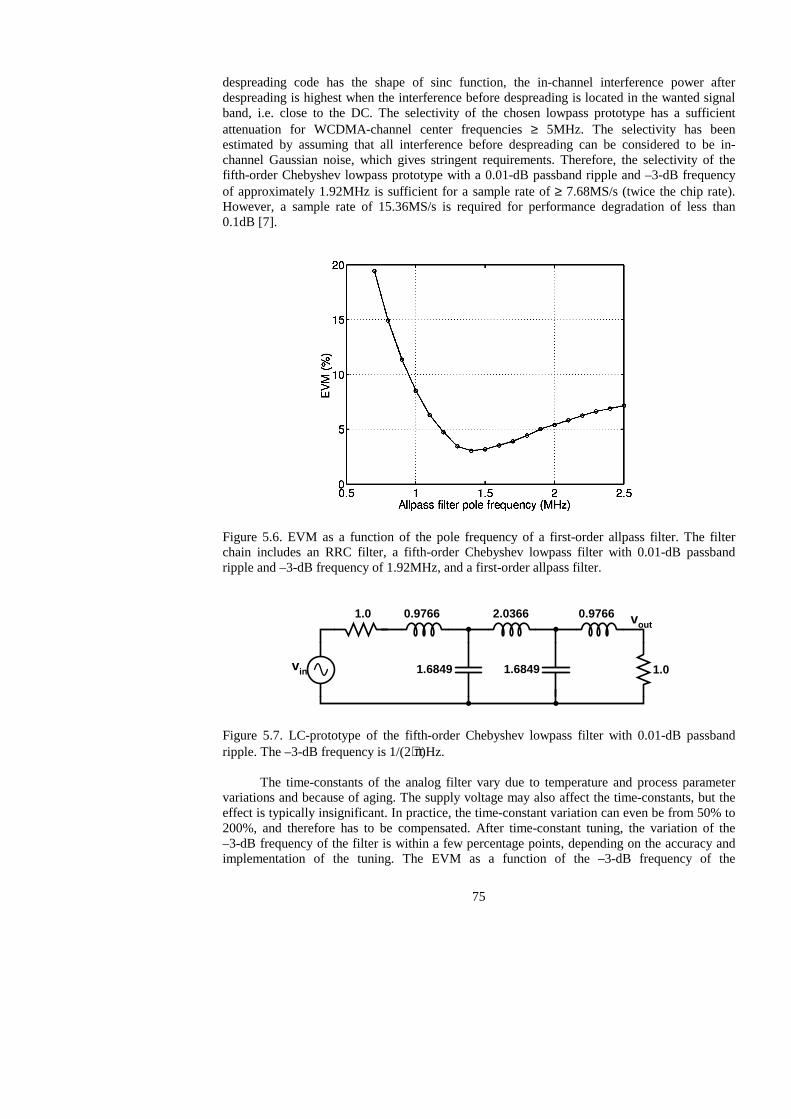
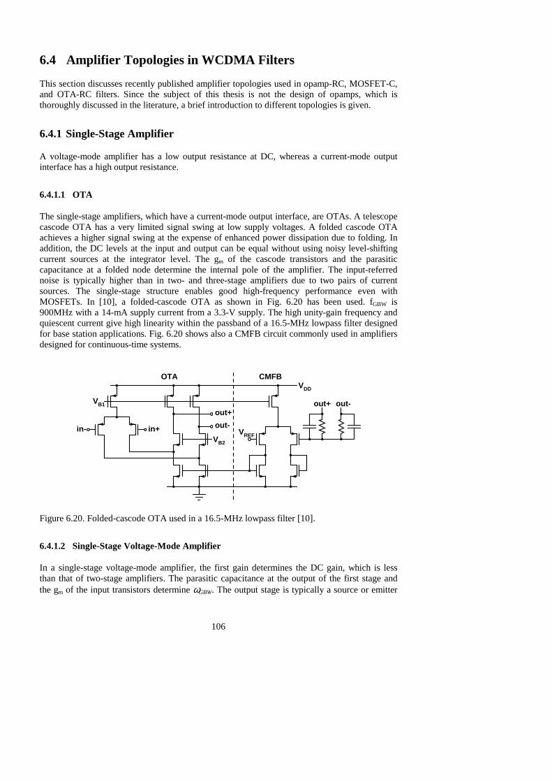
2 Direct-Conversion Receiver The superheterodyne radio has clearly been the dominant architecture in cellular radio receivers. Therefore, it is discussed as an introduction at the beginning of this chapter. Next, the direct-conversion architecture and its properties, both benefits and drawbacks, are explained and recent implementations reported in the literature summarized. The other radio receiver architectures are not discussed since they are beyond the scope of this thesis. The purpose of a radio receiver is to detect the potentially weak desired signal in the presence of noise and unwanted signals. The power of the other signals might be many orders of magnitude larger than the power of the desired signal channel. Because of the harsh environment, a high selectivity is required. The channel selection at radio frequency (RF) would require filters with very high quality factors and selectivity. In UTRA/FDD, the channel bandwidth and carrier frequency are approximately 4MHz and 2GHz, respectively. The channel-select filter quality factor would be 500 and the adjacent channel attenuation at a 5MHz frequency offset should be at least 33dB in a cellular phone [1]. In GSM, the signal bandwidth is only 200kHz, which increases the required quality factor to 4500, when the carrier frequency is 900MHz. The filter order should be at least five. Since such filters are not available, the problem has to be circumvented [2]. The solution to the problem is heterodyning, in which the RF signal is downconverted to an intermediate frequency (IF) using a local oscillator (LO) signal at a different frequency from the carrier. At a lower IF, the requirements for the channel-select filter become easier to achieve [3]. After selecting the desired signal channel, the transmitted information must be detected. In modern cellular systems, which use digital modulation and coding, the detection is performed digitally. Most of the signal processing is implemented in the digital domain where the limitations of the analog domain can be avoided. However, the direct digitization at RF is not technically possible at the moment, nor will it be in the near future because of the lack of appropriate ADCs. In the future, the analog front-end of the radio receiver will therefore remain necessary in order to reduce the dynamic range and maximum signal frequency before the analog-to-digital conversion. However, this interface is moving towards the antenna as a result of developments in analog-to-digital conversion techniques.
2.1 Superheterodyne Receiver
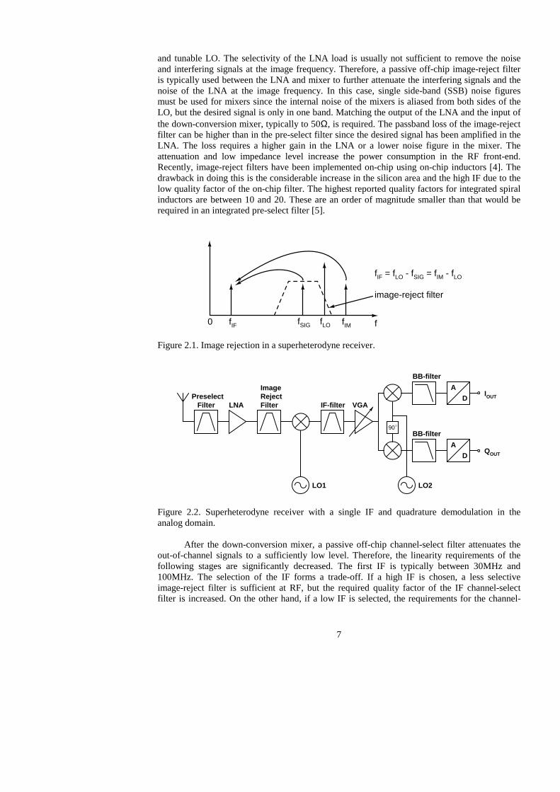
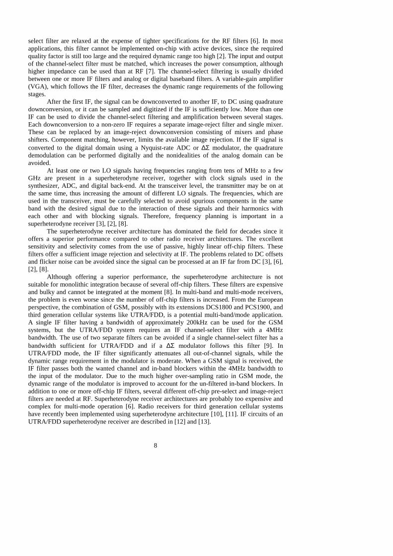
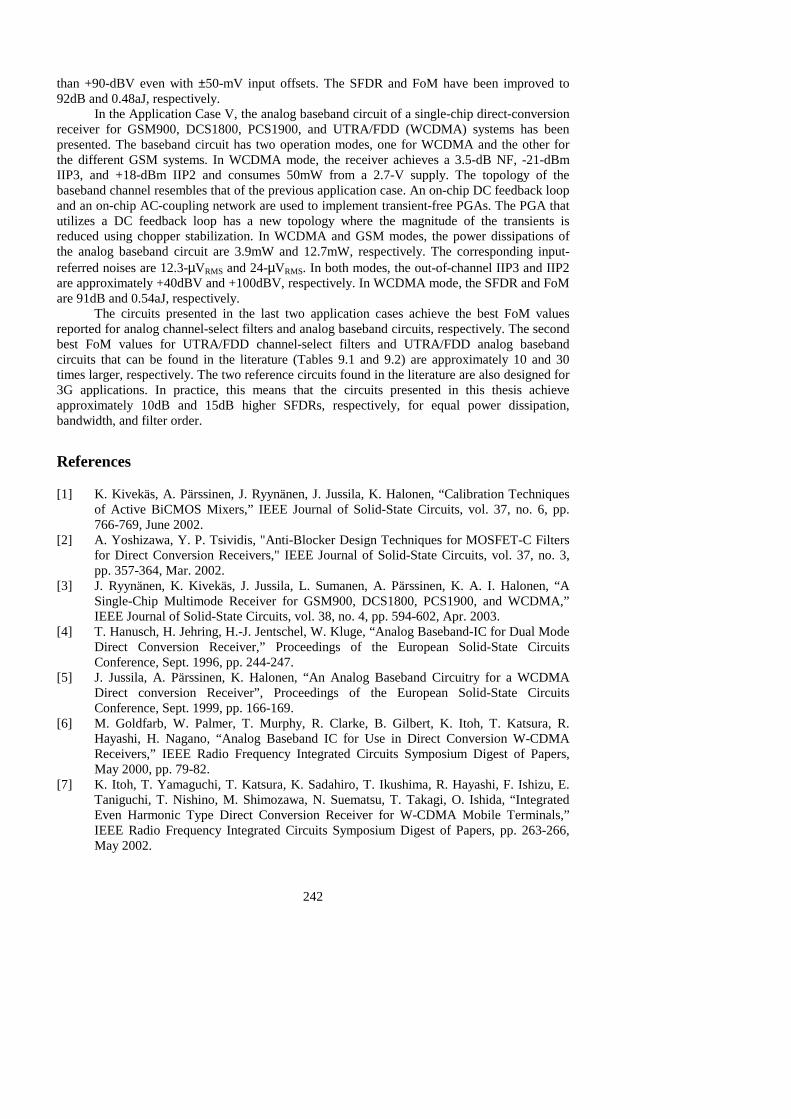
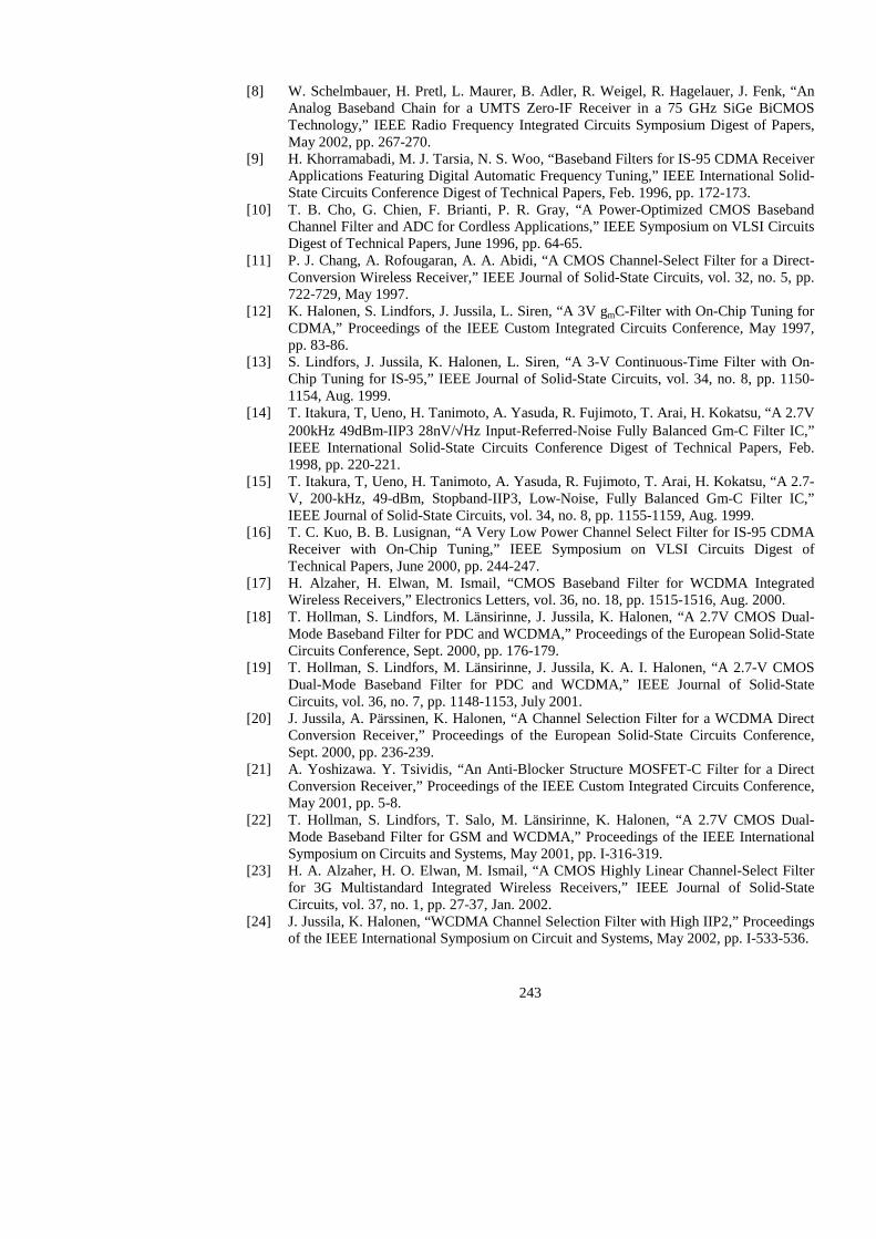
When the RF signal is downconverted to a non-zero IF, the image, which is at the same frequency offset from the LO as the desired RF signal, but on the other side of the LO, is mixed to the same IF as the desired signal. After downconversion using a single mixer, the image can not be separated from the desired signal [3]. In a superheterodyne receiver, the image signal is attenuated using an image-reject filter before each down-conversion stage, as shown in Fig. 2.1. The wanted signal is at frequency fSIG, LO at fLO, and the IF signal at fIF. The image frequency is fIM. A block diagram of a superheterodyne receiver is shown in Fig. 2.2. First, a passive off-chip pre-select filter attenuates the signals outside the desired system band. If the first IF is at least half of the system bandwidth, the pre-select filter also performs image rejection. The passband attenuation of the filter is critical since it directly adds to the receiver noise figure. A low-noise amplifier (LNA) follows the pre-select filter. The LNA input must be matched to a specified impedance level, typically 50Ω, since the matching impedance is part of the pre-select filter. After the LNA, the desired RF signal is downconverted to a fixed IF using a single mixer
7
and tunable LO. The selectivity of the LNA load is usually not sufficient to remove the noise and interfering signals at the image frequency. Therefore, a passive off-chip image-reject filter is typically used between the LNA and mixer to further attenuate the interfering signals and the noise of the LNA at the image frequency. In this case, single side-band (SSB) noise figures must be used for mixers since the internal noise of the mixers is aliased from both sides of the LO, but the desired signal is only in one band. Matching the output of the LNA and the input of the down-conversion mixer, typically to 50Ω, is required. The passband loss of the image-reject filter can be higher than in the pre-select filter since the desired signal has been amplified in the LNA. The loss requires a higher gain in the LNA or a lower noise figure in the mixer. The attenuation and low impedance level increase the power consumption in the RF front-end. Recently, image-reject filters have been implemented on-chip using on-chip inductors [4]. The drawback in doing this is the considerable increase in the silicon area and the high IF due to the low quality factor of the on-chip filter. The highest reported quality factors for integrated spiral inductors are between 10 and 20. These are an order of magnitude smaller than that would be required in an integrated pre-select filter [5].
image-reject filter
fIF = fLO - fSIG = fIM - fLO
f0 fIF fSIG fLO fIM Figure 2.1. Image rejection in a superheterodyne receiver.
LNA
A
D
A
D
90
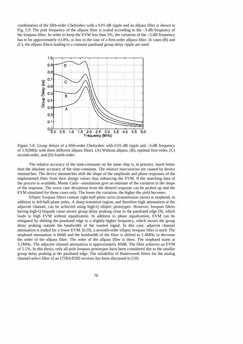
LO1 LO2
VGAFilter
Image
IF-filterRejectPreselect
Filter
BB-filter
BB-filter
IOUT
QOUT
Figure 2.2. Superheterodyne receiver with a single IF and quadrature demodulation in the analog domain. After the down-conversion mixer, a passive off-chip channel-select filter attenuates the out-of-channel signals to a sufficiently low level. Therefore, the linearity requirements of the following stages are significantly decreased. The first IF is typically between 30MHz and 100MHz. The selection of the IF forms a trade-off. If a high IF is chosen, a less selective image-reject filter is sufficient at RF, but the required quality factor of the IF channel-select filter is increased. On the other hand, if a low IF is selected, the requirements for the channel-
8
select filter are relaxed at the expense of tighter specifications for the RF filters [6]. In most applications, this filter cannot be implemented on-chip with active devices, since the required quality factor is still too large and the required dynamic range too high [2]. The input and output of the channel-select filter must be matched, which increases the power consumption, although higher impedance can be used than at RF [7]. The channel-select filtering is usually divided between one or more IF filters and analog or digital baseband filters. A variable-gain amplifier (VGA), which follows the IF filter, decreases the dynamic range requirements of the following stages. After the first IF, the signal can be downconverted to another IF, to DC using quadrature downconversion, or it can be sampled and digitized if the IF is sufficiently low. More than one IF can be used to divide the channel-select filtering and amplification between several stages. Each downconversion to a non-zero IF requires a separate image-reject filter and single mixer. These can be replaced by an image-reject downconversion consisting of mixers and phase shifters. Component matching, however, limits the available image rejection. If the IF signal is converted to the digital domain using a Nyquist-rate ADC or ∆Σ modulator, the quadrature demodulation can be performed digitally and the nonidealities of the analog domain can be avoided. At least one or two LO signals having frequencies ranging from tens of MHz to a few GHz are present in a superheterodyne receiver, together with clock signals used in the synthesizer, ADC, and digital back-end. At the transceiver level, the transmitter may be on at the same time, thus increasing the amount of different LO signals. The frequencies, which are used in the transceiver, must be carefully selected to avoid spurious components in the same band with the desired signal due to the interaction of these signals and their harmonics with each other and with blocking signals. Therefore, frequency planning is important in a superheterodyne receiver [3], [2], [8]. The superheterodyne receiver architecture has dominated the field for decades since it offers a superior performance compared to other radio receiver architectures. The excellent sensitivity and selectivity comes from the use of passive, highly linear off-chip filters. These filters offer a sufficient image rejection and selectivity at IF. The problems related to DC offsets and flicker noise can be avoided since the signal can be processed at an IF far from DC [3], [6], [2], [8]. Although offering a superior performance, the superheterodyne architecture is not suitable for monolithic integration because of several off-chip filters. These filters are expensive and bulky and cannot be integrated at the moment [8]. In multi-band and multi-mode receivers, the problem is even worse since the number of off-chip filters is increased. From the European perspective, the combination of GSM, possibly with its extensions DCS1800 and PCS1900, and third generation cellular systems like UTRA/FDD, is a potential multi-band/mode application. A single IF filter having a bandwidth of approximately 200kHz can be used for the GSM systems, but the UTRA/FDD system requires an IF channel-select filter with a 4MHz bandwidth. The use of two separate filters can be avoided if a single channel-select filter has a bandwidth sufficient for UTRA/FDD and if a ∆Σ modulator follows this filter [9]. In UTRA/FDD mode, the IF filter significantly attenuates all out-of-channel signals, while the dynamic range requirement in the modulator is moderate. When a GSM signal is received, the IF filter passes both the wanted channel and in-band blockers within the 4MHz bandwidth to the input of the modulator. Due to the much higher over-sampling ratio in GSM mode, the dynamic range of the modulator is improved to account for the un-filtered in-band blockers. In addition to one or more off-chip IF filters, several different off-chip pre-select and image-reject filters are needed at RF. Superheterodyne receiver architectures are probably too expensive and complex for multi-mode operation [6]. Radio receivers for third generation cellular systems have recently been implemented using superheterodyne architecture [10], [11]. IF circuits of an UTRA/FDD superheterodyne receiver are described in [12] and [13].
9
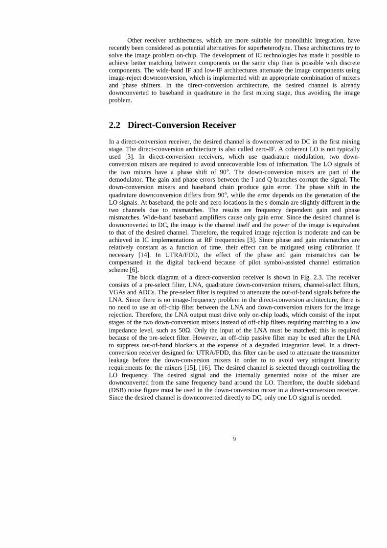
Other receiver architectures, which are more suitable for monolithic integration, have recently been considered as potential alternatives for superheterodyne. These architectures try to solve the image problem on-chip. The development of IC technologies has made it possible to achieve better matching between components on the same chip than is possible with discrete components. The wide-band IF and low-IF architectures attenuate the image components using image-reject downconversion, which is implemented with an appropriate combination of mixers and phase shifters. In the direct-conversion architecture, the desired channel is already downconverted to baseband in quadrature in the first mixing stage, thus avoiding the image problem.
2.2 Direct-Conversion Receiver
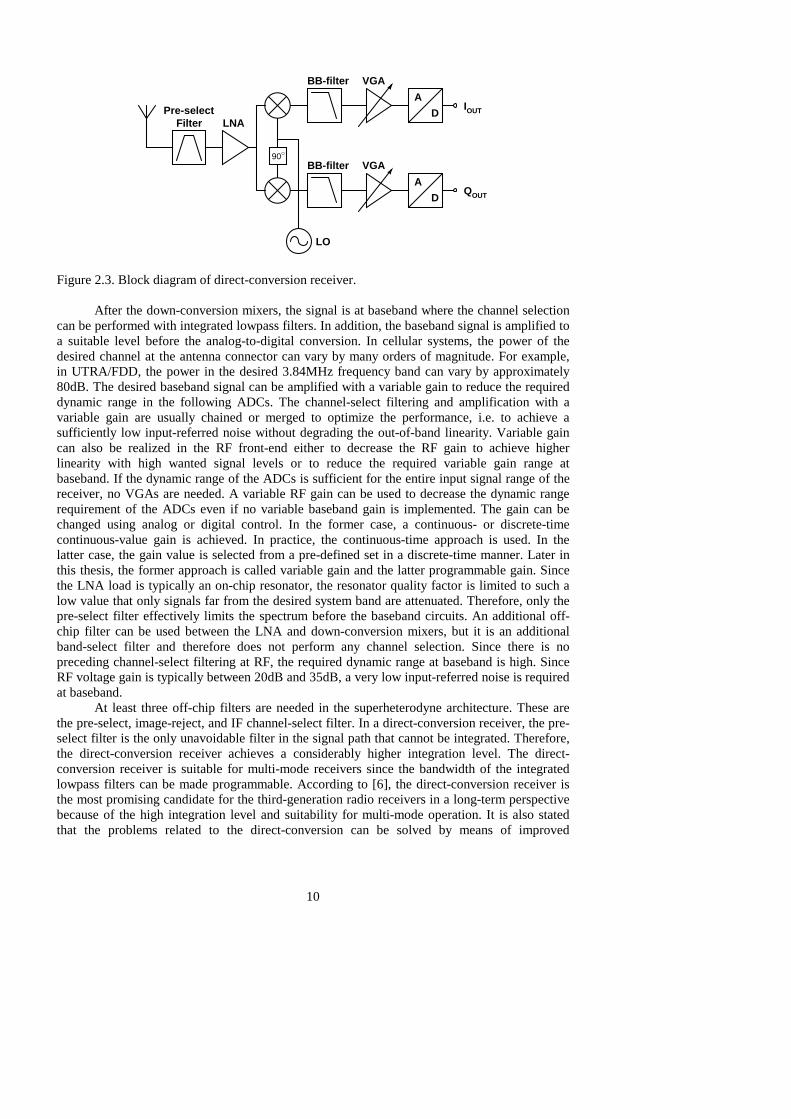
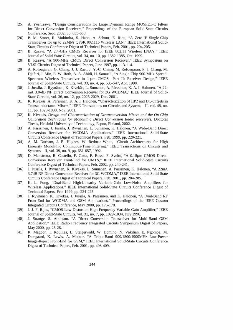
In a direct-conversion receiver, the desired channel is downconverted to DC in the first mixing stage. The direct-conversion architecture is also called zero-IF. A coherent LO is not typically used [3]. In direct-conversion receivers, which use quadrature modulation, two down-conversion mixers are required to avoid unrecoverable loss of information. The LO signals of the two mixers have a phase shift of 90°. The down-conversion mixers are part of the demodulator. The gain and phase errors between the I and Q branches corrupt the signal. The down-conversion mixers and baseband chain produce gain error. The phase shift in the quadrature downconversion differs from 90°, while the error depends on the generation of the LO signals. At baseband, the pole and zero locations in the s-domain are slightly different in the two channels due to mismatches. The results are frequency dependent gain and phase mismatches. Wide-band baseband amplifiers cause only gain error. Since the desired channel is downconverted to DC, the image is the channel itself and the power of the image is equivalent to that of the desired channel. Therefore, the required image rejection is moderate and can be achieved in IC implementations at RF frequencies [3]. Since phase and gain mismatches are relatively constant as a function of time, their effect can be mitigated using calibration if necessary [14]. In UTRA/FDD, the effect of the phase and gain mismatches can be compensated in the digital back-end because of pilot symbol-assisted channel estimation scheme [6]. The block diagram of a direct-conversion receiver is shown in Fig. 2.3. The receiver consists of a pre-select filter, LNA, quadrature down-conversion mixers, channel-select filters, VGAs and ADCs. The pre-select filter is required to attenuate the out-of-band signals before the LNA. Since there is no image-frequency problem in the direct-conversion architecture, there is no need to use an off-chip filter between the LNA and down-conversion mixers for the image rejection. Therefore, the LNA output must drive only on-chip loads, which consist of the input stages of the two down-conversion mixers instead of off-chip filters requiring matching to a low impedance level, such as 50Ω. Only the input of the LNA must be matched; this is required because of the pre-select filter. However, an off-chip passive filter may be used after the LNA to suppress out-of-band blockers at the expense of a degraded integration level. In a direct-conversion receiver designed for UTRA/FDD, this filter can be used to attenuate the transmitter leakage before the down-conversion mixers in order to to avoid very stringent linearity requirements for the mixers [15], [16]. The desired channel is selected through controlling the LO frequency. The desired signal and the internally generated noise of the mixer are downconverted from the same frequency band around the LO. Therefore, the double sideband (DSB) noise figure must be used in the down-conversion mixer in a direct-conversion receiver. Since the desired channel is downconverted directly to DC, only one LO signal is needed.
10
LNA
A
D
A
D
90
LO
Pre-selectFilter
BB-filter
BB-filter
IOUT
QOUT
VGA
VGA
Figure 2.3. Block diagram of direct-conversion receiver. After the down-conversion mixers, the signal is at baseband where the channel selection can be performed with integrated lowpass filters. In addition, the baseband signal is amplified to a suitable level before the analog-to-digital conversion. In cellular systems, the power of the desired channel at the antenna connector can vary by many orders of magnitude. For example, in UTRA/FDD, the power in the desired 3.84MHz frequency band can vary by approximately 80dB. The desired baseband signal can be amplified with a variable gain to reduce the required dynamic range in the following ADCs. The channel-select filtering and amplification with a variable gain are usually chained or merged to optimize the performance, i.e. to achieve a sufficiently low input-referred noise without degrading the out-of-band linearity. Variable gain can also be realized in the RF front-end either to decrease the RF gain to achieve higher linearity with high wanted signal levels or to reduce the required variable gain range at baseband. If the dynamic range of the ADCs is sufficient for the entire input signal range of the receiver, no VGAs are needed. A variable RF gain can be used to decrease the dynamic range requirement of the ADCs even if no variable baseband gain is implemented. The gain can be changed using analog or digital control. In the former case, a continuous- or discrete-time continuous-value gain is achieved. In practice, the continuous-time approach is used. In the latter case, the gain value is selected from a pre-defined set in a discrete-time manner. Later in this thesis, the former approach is called variable gain and the latter programmable gain. Since the LNA load is typically an on-chip resonator, the resonator quality factor is limited to such a low value that only signals far from the desired system band are attenuated. Therefore, only the pre-select filter effectively limits the spectrum before the baseband circuits. An additional off-chip filter can be used between the LNA and down-conversion mixers, but it is an additional band-select filter and therefore does not perform any channel selection. Since there is no preceding channel-select filtering at RF, the required dynamic range at baseband is high. Since RF voltage gain is typically between 20dB and 35dB, a very low input-referred noise is required at baseband. At least three off-chip filters are needed in the superheterodyne architecture. These are the pre-select, image-reject, and IF channel-select filter. In a direct-conversion receiver, the pre-select filter is the only unavoidable filter in the signal path that cannot be integrated. Therefore, the direct-conversion receiver achieves a considerably higher integration level. The direct-conversion receiver is suitable for multi-mode receivers since the bandwidth of the integrated lowpass filters can be made programmable. According to [6], the direct-conversion receiver is the most promising candidate for the third-generation radio receivers in a long-term perspective because of the high integration level and suitability for multi-mode operation. It is also stated that the problems related to the direct-conversion can be solved by means of improved
11
semiconductor technology and a system-level-based optimization of the circuits and their design. It is more difficult to say which architecture, superheterodyne or direct conversion, leads to lower power consumption. In a direct-conversion receiver, there is no need to drive the signal off the chip at RF and IF. The interfaces to the off-chip filters are typically matched to quite low impedances, which are power-hungry. The quadrature downconversion at RF in a direct-conversion receiver consumes more power than the quadrature downconversion at IF in a superheterodyne solution. Since there is no passive channel-select filter before the baseband circuitry, the dynamic range requirement of the baseband part is considerably higher in a direct-conversion receiver. A sufficient dynamic range at the baseband may require a considerable amount of power. In the superheterodyne architecture, a passive IF filter attenuates the out-of-band signals, decreasing significantly the dynamic range requirement of the baseband circuit. In a direct-conversion receiver, two high-performance active filters are required. On the other hand, in a direct-conversion receiver, there is no IF circuitry at all. Signal processing at an IF consumes more power than at the baseband because of the higher operation frequency. Direct-conversion radio receivers have been used in commercial digital phones since 1991 [5]. Tables 2.1 and 2.2 summarize recently published data on direct-conversion receivers and RF front-ends for direct-conversion receivers. Tables 2.1 and 2.2 do not contain the I/Q imbalance results since in UTRA/FDD systems the imbalances can be estimated and compensated [6]. The direct-conversion architecture suffers from several drawbacks, which make the design of a high-performance receiver a challenging task. These include DC offsets due to device mismatches and self-mixing of the LO, RF signal self-mixing as a result of leakage to the LO port, distortion due to even-order nonlinearities, flicker noise, and leakage of the LO signal out from the antenna [17], [14], [3], [8]. The LO signal is in the passband of the LNA, mixers, and off-chip RF filters. The LO signal leaks to the LNA input and to the input of the down-conversion mixers. If the LO leaks to the LNA input, it is amplified with the LNA gain. The leaked LO signal is downconverted with itself, resulting in a constant DC offset. The level of the offset depends on the amount of leakage and the phase shift between the LO signal and leakage. The resulting DC offset at the mixer output can be orders of magnitude larger than the desired signal. If the RF gain is changed, the level of the LO leakage at the mixer input is altered, resulting in a change in the DC offset at the mixer output. A change in the phase is also possible. The DC offset change can be much higher than the wanted signal [18]. For example, in [19], the LO-to-RF isolation is 65dB, while the LO power can be as high as 0dBm. This results in a leaked LO signal of –65dBm at the LNA input, which is 52dB higher than the wanted channel in the UTRA/FDD reference sensitivity test case [1]. An effective method to mitigate the amount of LO signal at the LNA input is to use a double-frequency LO, from which the LO is generated on-chip using a divide-by-two circuit. Since the LO signal is at the passband of the pre-selection filter, it can leak out from the antenna and reflect back. The LO signal leaking out from the antenna interferes with other receivers in the system. Wireless standards specify a maximum amount of spurious LO emission, which can range from –50dBm to –80dBm [14]. In UTRA/FDD, the spurious LO emission of a cellular phone must not exceed –60dBm/3.84MHz at the antenna connector [1]. The leaked LO signal may reflect back from external objects. Since the environment may change and may contain moving objects, the level and phase of the reflected LO signal can change. The result is a time-varying DC offset. The efficiency of the DC offset removal scheme in this case depends on the frequency content of the reflected LO signal. If the LO signal is reflected back from moving objects, the result is a Doppler shift in the frequency of the reflected signal. Therefore, the reflected LO signal is downconverted to a non-zero baseband frequency, which depends on the speed of the external moving object [20], [21]. The
12
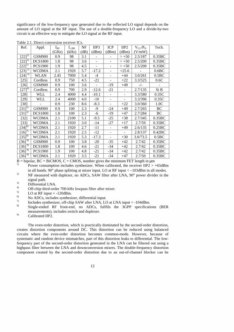
significance of the low-frequency spur generated due to the reflected LO signal depends on the amount of LO signal at the RF input. The use of a double-frequency LO and a divide-by-two circuit is an effective way to mitigate the LO signal at the RF input. Table 2.1. Direct-conversion receiver ICs.
B = bipolar, BC = BiCMOS, C = CMOS, number gives the minimum FET length in µm 1) Power consumption includes synthesizer. When calibrated, the receiver IIP2 > +65dBm
in all bands. 90° phase splitting at mixer input. LO at RF input < –103dBm in all modes. 2) NF measured with duplexer, no ADCs, SAW filter after LNA, 90° power divider in the
signal path. 3) Differential LNA. 4) Off-chip third-order 700-kHz lowpass filter after mixer. 5) LO at RF input = -120dBm. 6) No ADCs, includes synthesizer, differential input. 7) Includes synthesizer, off-chip SAW after LNA, LO at LNA input = -104dBm. 8) Single-ended RF front-end, no ADCs, fullfils the 3GPP specifications (BER
measurements), includes switch and duplexer. 9) Calibrated IIP2. The even-order distortion, which is practically dominated by the second-order distortion, creates distortion components around DC. This distortion can be reduced using balanced circuits where the even-order distortion becomes common-mode. However, because of systematic and random device mismatches, part of this distortion leaks to differential. The low-frequency part of the second-order distortion generated in the LNA can be filtered out using a highpass filter between the LNA and downconversion mixers. The double-frequency distortion component created by the second-order distortion due to an out-of-channel blocker can be
13
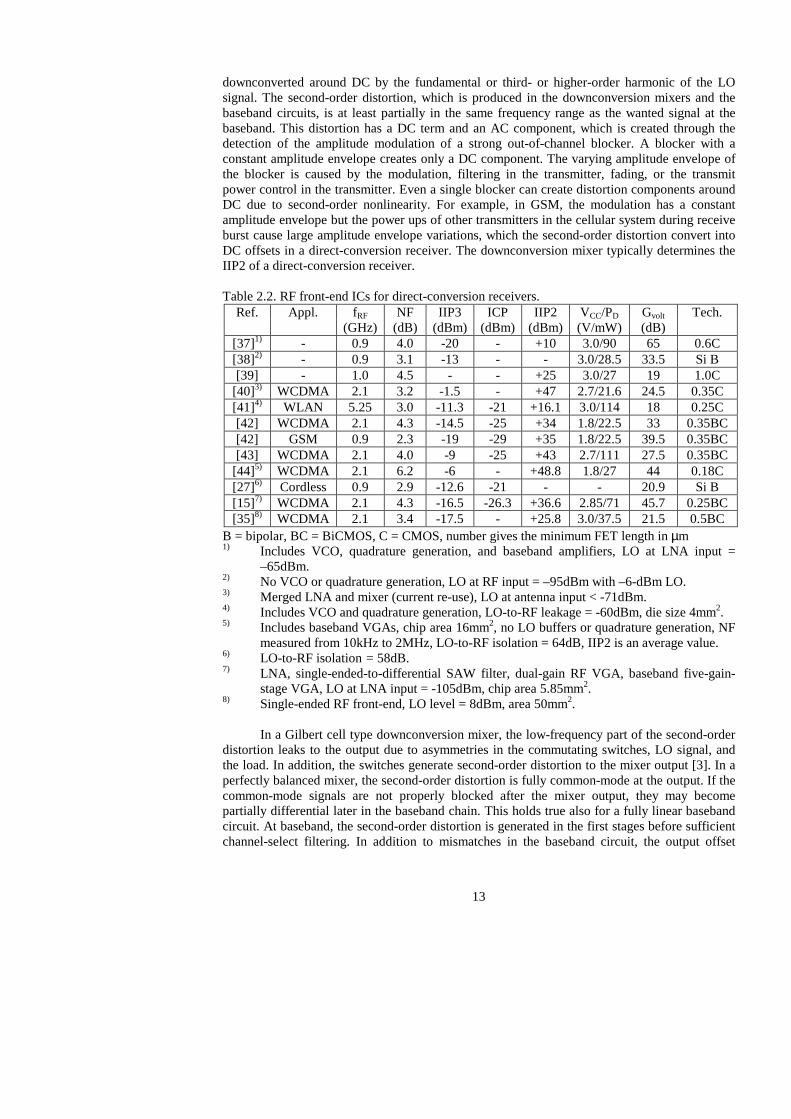
downconverted around DC by the fundamental or third- or higher-order harmonic of the LO signal. The second-order distortion, which is produced in the downconversion mixers and the baseband circuits, is at least partially in the same frequency range as the wanted signal at the baseband. This distortion has a DC term and an AC component, which is created through the detection of the amplitude modulation of a strong out-of-channel blocker. A blocker with a constant amplitude envelope creates only a DC component. The varying amplitude envelope of the blocker is caused by the modulation, filtering in the transmitter, fading, or the transmit power control in the transmitter. Even a single blocker can create distortion components around DC due to second-order nonlinearity. For example, in GSM, the modulation has a constant amplitude envelope but the power ups of other transmitters in the cellular system during receive burst cause large amplitude envelope variations, which the second-order distortion convert into DC offsets in a direct-conversion receiver. The downconversion mixer typically determines the IIP2 of a direct-conversion receiver. Table 2.2. RF front-end ICs for direct-conversion receivers.
B = bipolar, BC = BiCMOS, C = CMOS, number gives the minimum FET length in µm 1) Includes VCO, quadrature generation, and baseband amplifiers, LO at LNA input =
–65dBm. 2) No VCO or quadrature generation, LO at RF input = –95dBm with –6-dBm LO. 3) Merged LNA and mixer (current re-use), LO at antenna input < -71dBm. 4) Includes VCO and quadrature generation, LO-to-RF leakage = -60dBm, die size 4mm2. 5) Includes baseband VGAs, chip area 16mm2, no LO buffers or quadrature generation, NF
measured from 10kHz to 2MHz, LO-to-RF isolation = 64dB, IIP2 is an average value. 6) LO-to-RF isolation = 58dB. 7) LNA, single-ended-to-differential SAW filter, dual-gain RF VGA, baseband five-gain-
stage VGA, LO at LNA input = -105dBm, chip area 5.85mm2. 8) Single-ended RF front-end, LO level = 8dBm, area 50mm2. In a Gilbert cell type downconversion mixer, the low-frequency part of the second-order distortion leaks to the output due to asymmetries in the commutating switches, LO signal, and the load. In addition, the switches generate second-order distortion to the mixer output [3]. In a perfectly balanced mixer, the second-order distortion is fully common-mode at the output. If the common-mode signals are not properly blocked after the mixer output, they may become partially differential later in the baseband chain. This holds true also for a fully linear baseband circuit. At baseband, the second-order distortion is generated in the first stages before sufficient channel-select filtering. In addition to mismatches in the baseband circuit, the output offset
14
voltage or current (depending on the type of the mixer-baseband interface) affects the balance of the baseband circuit, and therefore the amount of second-order distortion. RF self-mixing occurs when a strong out-of-channel blocking signal leaks to the LO port of a down-conversion mixer and becomes downconverted with itself. The resulting distortion component has a DC term and a spectrum, which depend on the amplitude modulation and average power of the blocker. In addition, the phase shift between the blocking signals at the RF and LO ports of the mixer affects the resulting distortion component. When there is no phase shift, the result is similar to the second-order distortion [3]. The resulting offset at the mixer output is in the range of some millivolts [6]. DC offset cancellation schemes are effective only in removing the constant DC offset. Since it is very difficult to remove the in-channel baseband distortion component due to RF self-mixing of an amplitude modulated blocker after the downconversion, the leakage of a strong signal to the LO port of a mixer should be suppressed to a sufficiently low level. In UTRA/FDD, the transmitter may be on simultaneously with the receiver. Although the transmitter signal is attenuated in the pre-select filter, it is probably the strongest interfering signal at the input of the LNA. If the leakage is not filtered out using an off-chip bandpass filter between the LNA and mixers, it sets the specifications for the isolation between the mixer ports. The flicker noise generated in the down-conversion mixer switching transistors and the first baseband circuits before a sufficient amplification can degrade the noise performance of a receiver significantly, especially in narrow-band systems. This is particularly a problem in CMOS receivers since the flicker noise in MOS transistors is considerably higher than in bipolar devices. The flicker noise has to be taken into account even in wide-band direct-conversion receivers. In practice, DC offsets cannot be reduced to sufficiently low levels by improved circuit design without any compensation. Therefore, circuits that remove the DC offsets have to be used. DC offset removal is not necessary in the analog domain if the baseband gain is low and the dynamic range in the analog-to-digital conversion is sufficient to tolerate the DC offsets, which can be orders of magnitude larger than the desired signal. Then, the DC offsets can be removed in the digital domain. The component mismatches and the LO self-mixing produce constant DC offsets. In cellular systems having a continuous reception, the constant DC offsets can be filtered out using capacitive coupling in the signal path or a low-frequency DC feedback loop, i.e. servo. The feedback is a first-order lowpass filter or an integrator. The feedback may be in the analog domain or partly in the digital. Both DC offset removal schemes form a highpass filter in the signal path. In spectrally efficient modulation schemes used in modern cellular systems, the maximum of the baseband signal spectrum is at DC. Highpass filtering removes part of the signal and causes inter-symbol-interference (ISI) to the signal. The –3-dB frequency of the highpass filter must be small compared to the signal bandwidth to avoid significant signal degradation. Because of the low –3-dB frequencies, large silicon areas are required to implement these time constants on-chip. The highpass filters suffer from long settling times. If the baseband gain is limited to such a low value that the DC offsets cannot saturate the ADCs or ∆Σ modulators, the DC offset can be removed in the digital domain. In addition, the constant DC offset can be measured and removed from the input signal before the ADC, which improves the dynamic range of the back-end of the analog baseband circuit and ADCs. In burst-mode operated systems, like GSM, the DC offsets can be measured during idle modes. The stored DC offset can be removed from the signal during the receiver burst since the DC offsets, because of mismatches and LO self-mixing, in practice remain constant during a single burst. During a receiver burst there is no highpass filter degrading the signal quality. However, the dynamic range in the back-end of the receiver has to be sufficient to account for the changes in the DC offsets. Slowly changing DC offsets can be mitigated using highpass filters if the rate of change is low enough. Methods to remove DC offsets are discussed in more detail later in this thesis.
15
The wide-band distortion components generated due to self-mixing or second-order distortion by blockers, which use modulation schemes having amplitude modulation, cannot be removed using highpass filters or digital averaging algorithms. The DC offset may also change abruptly. A change in the RF gain, which alters the amount of LO self-mixing, a change in the LO frequency, a change in the baseband gain, or an out-of-channel blocker that experiences a step in the average power at the receiver input, can cause such a transition. The blocker causes a transition due to self-mixing or second-order distortion. The analog or digital highpass filters cannot filter out these fast transitions. However, the variations in the DC offset can be removed in the digital domain using real-time averaging algorithms when the received signal has a constant amplitude envelope. In GSM direct-conversion receivers, the dynamic offsets have been handled succesfully using these algorithms [5], [45]. The removal of DC offsets is discussed in detail later in this thesis. In direct-conversion radio receivers having a continuous reception, it may be necessary to change the gain at baseband during reception. This may lead to problems [19]. In balanced circuits, device mismatches in active and passive components, which may carry DC currents and which are DC coupled to the output, produce static DC offsets. If the state of the circuit is changed - for example, the baseband gain is altered - then the DC offsets change if the change is performed in devices that may carry DC currents. The offsets at the mixer output can be orders of magnitude larger than the wanted signal. In UTRA/FDD, the reception is continuous without idle times. Therefore, the gain of the signal channel must be changed during the reception without degrading the signal quality. In radio receivers designed for modern cellular systems, it is desirable to be able to use digitally controlled gain in discrete steps, since then the gain can be controlled by the DSP. This simplifies the gain control scheme and circuitry. However, if the baseband gain is changed in discrete steps during reception, the DC offsets at the output can be changed abruptly. The reasons for the transients are the random device mismatches in the baseband circuit and the amplification of preceding DC offsets with a programmable gain. The highpass filters in the signal path filter out these steps but they are only slowly attenuated, which may degrade the signal quality. The steps in the output can be avoided if the gain is changed in such a manner that the biasing of the circuit is preserved accurately, even in the presence of mismatches and asymmetries, and if the preceding DC offsets are not amplified with a programmable gain. These structures are part of a highpass filter. However, the out-of-band blocking signals may still cause transients because of the parasitic capacitances in the switched nodes. This issue is discussed and solutions for mitigating the transients are presented later in this thesis.
References
[1] 3rd Generation Partnership Project, Technical Specification Group Radio Access Networks, UE Radio Transmission and Reception (FDD), 3GPP TS 25.101, v.5.0.0, Sept. 2001.
[2] S. Lindfors, CMOS Baseband Integrated Circuit Techniques for Radio Receivers, Doctoral Thesis, Helsinki University of Finland, Espoo, Finland, 2000.
[3] A. Pärssinen, Direct Conversion Receivers in Wide-Band Systems, Kluwer Academic Publishers, Dordrecht, The Netherlands, 2001.
[4] R. Magoon, I. Koullias, L. Steigerwald, W. Domino, N. Vakilian, E. Ngompe, M. Damgaard, K. Lewis, A. Molnar, ”A Triple-Band 900/1800/1900MHz Low-Power Image-Reject Front-End for GSM,” IEEE International Solid-State Circuits Conference Digest of Technical Papers, Feb. 2001, pp. 408-409.
[5] J. Sevenhans, B. Verstraeten, S. Taraborrelli, “Trends in Silicon Radio Large Scale Integration: Zero IF Receiver! Zero I & Q Transmitter! Zero Discrete Passives!,” IEEE Communications Magazine, pp. 142-147, Jan. 2000.
16
[6] A. Springer, L. Maurer, R. Weigel, “RF System Concepts for Highly Integrated RFICs for W-CDMA Mobile Radio Terminals,” IEEE Transactions on Microwave Theory and Techniques, vol. 50, no. 1, pp. 254-267, Jan. 2002.
[7] P. Orsatti, F. Piazza, Q. Huang, “A 20-mA-Receive, 55-mA-Transmit, Single-Chip GSM Transceiver in 0.25-µm CMOS,” IEEE Journal of Solid-State Circuits, vol. 34, no. 12, pp. 1869-1880, Dec. 1999.
[8] C. R. Iversen, A UTRA/FDD Receiver Architecture and LNA in CMOS Technology, Ph.D. Thesis, Aalborg University, Aalborg, Denmark, 2001.
[9] T. Salo, T. Hollman, S. Lindfors, K. Halonen, “A Dual-Mode 80MHz Bandpass ∆Σ Modulator for a GSM/WCDMA IF-Receiver,” IEEE International Solid-State Circuits Conference Digest of Technical Papers, Feb. 2002, pp. 218-219.
[10] K. Lim, C.-H. Park, H. K. Ahn, J. J. Kim, B. Kim, “A Fully Integrated CMOS RF Front-End with On-Chip VCO for WCDMA Applications,” IEEE International Solid-State Circuits Conference Digest of Technical Papers, Feb. 2001, pp. 286-287.
[11] V. Aparin, P. Gazzerro, J. Zhou, B. Sun, S. Szabo, E. Zeisel, T. Segoria, S. Ciccarelli, C. Persico, C. Narathong, R. Sridhara, “A Highly-Integrated Tri-Band/Quad-Mode SiGe BiCMOS RF-to-Baseband Receiver for Wireless CDMA/WCDMA/AMPS Applications with GPS Capability,” IEEE International Solid-State Circuits Conference Digest of Technical Papers, Feb. 2002, pp. 234-235.
[12] W. Thomann, J. Fenk, R. Hagelauer, R. Weigel, “Fully Integrated W-CDMA IF Receiver and Transmitter Including IF Synthesizer and On-Chip VCO for UMTS Mobiles,” IEEE Journal of Solid-State Circuits, vol. 36, no. 9, pp. 1407-1419, Sept. 2001.
[13] U. Dasgupta, W. G. Yeoh, C. G. Tan, S. J. Wong, H. Mori, R. Singh, M. Itoh, “A CMOS Transmit/Receive IF Chip-Set for WCDMA Mobiles,” IEEE Radio Frequency Integrated Circuits Symposium Digest of Papers, May 2002, pp. 195-198.
[14] B. Razavi, “Design Considerations for Direct-Conversion Receivers,” IEEE Transactions on Circuits and Systems—II: vol. 46, no. 6, pp. 428-435, June 1997
[15] D. Y. C. Lie, J. Kennedy, D. Livezey, B. Yang, T. Robinson, N. Sornin, T. Beukema, L. E. Larson, A. Senior, C. Saint, J. Blonski, N. Swanberg, P. Pawlowski, D. Gonya, X. Yuan, H. Zamat, “A Direct-Conversion W-CDMA Front-End SiGe Receiver Chip,” IEEE Radio Frequency Integrated Circuits Symposium Digest of Papers, May 2002, pp. 31-34.
[16] R. Gharpurey, N. Yanduru, F. Dantoni, P. Litmanen, G. Sirna, T. Mayhugh, C. Lin, I. Deng, P. Fontaine, F. Lin, “A Direct Conversion Receiver for the 3G WCDMA Standard,” Proceedings of the IEEE Custom Integrated Circuits Conference, May 2002, pp. 239-242.
[17] A. A. Abidi, “Direct-Conversion Radio Transceivers for Digital Communications,” IEEE Journal of Solid-State Circuits, vol. 30, no. 12, pp. 1399-1410, Dec. 1995.
[18] J. Ryynänen, K. Kivekäs, J. Jussila, A. Pärssinen, K. Halonen, “RF Gain Control in Direct Conversion Receivers,” Proceedings of the IEEE International Symposium on Circuit and Systems, May 2002, pp. IV-117-120.
[19] J. Jussila, J. Ryynänen, K. Kivekäs, L. Sumanen, A. Pärssinen, K. Halonen, “A 22mA 3.7dB NF Direct Conversion Receiver for 3G WCDMA,” IEEE International Solid-State Circuits Conference Digest of Technical Papers, Feb. 2001, pp. 284-285.
[20] J. H. Mikkelsen, T. E. Kolding, T. Larsen, T. Klingenbrunn, K. I. Pedersen, P. Mogensen, “Feasibility Study of DC Offset Filtering for UTRA-FDD/WCDMA Direct-Conversion Receiver,” Proceedings of the Norchip Conference, Nov. 1999, pp. 34-39.
[21] S. Laursen, Second Order Distortion in CMOS Integrator Mixers, Ph.D. Thesis, Aalborg University, Aalborg, Denmark, 2001.
17
[22] A. Molnar, R. Magoon, G. Hatcher, J. Zachan, W. Rhee, M. Damgaard, W. Domino, N. Vakilian, “A Single-Chip Quad-Band (850/900/1800/1900MHz) Direct-Conversion GSM/GPRS RF Transceiver with Integrated VCOs and Fractional-N Synthesizer,” IEEE International Solid-State Circuits Conference Digest of Technical Papers, Feb. 2002, pp. 232-233.
[23] K. Itoh, T. Katsura, H. Nagano, T. Yamaguchi, Y. Hamade, M. Shimozawa, N. Suematsu, R. Hayashi, W. Palmer, M. Goldfarb, “2GHz Band Even Harmonic Type Direct Conversion Receiver with ABB-IC for W-CDMA Mobile Terminal,” IEEE MTT-S International Microwave Symposium Digest, May 2000, pp. 1957-1960.
[24] P. M. Stroet, R. Mohindra, S. Hahn, A. Schuur, E. Riou, “A Zero-IF Single-Chip Transceiver for up to 22Mb/s QPSK 802.11b Wireless LAN,” IEEE International Solid-State Circuits Conference Digest of Technical Papers, Feb. 2001, pp. 204-205.
[25] T. Cho, E. Dukatz, M. Mack, D. MacNally, M. Marringa, S. Mehta, C. Nilson, L. Plouvier, S. Rabii, “A Single-Chip CMOS Direct-Conversion Transceiver for 900MHz Spread-Spectrum Digital Cordless Phones,” IEEE International Solid-State Circuits Conference Digest of Technical Papers, Dec. 1999, pp. 228-229.
[26] J. Strange, S. Atkinson, “A Direct Conversion Transceiver for Multi-Band GSM Application,” IEEE Radio Frequency Integrated Circuits Symposium Digest of Papers, May 2000, pp. 25-28.
[27] C. D. Hull, J. L. Tham, R. R. Chu, “A Direct-Conversion Receiver for 900MHz (ISM Band) Spread-Spectrum Digital Cordless Telephone,” IEEE Journal of Solid-State Circuits, vol. 31, no. 12, pp. 1955-1963, Dec. 1996.
[28] K. Lee, J. Park, J.-W. Lee, S.-W. Lee, H.-K. Huh, D.-K. Jeong, W. Kim, “A single-Chip 2.4GHz Direct-Conversion CMOS Receiver for Wireless Local Loop using One-Third Frequency Local Oscillator,” IEEE Symposium on VLSI Circuits Digest of Technical Papers, June 2000, pp. 42-45.
[29] K. Lee, J. Park, J.-W. Lee, S.-W. Lee, H.-K. Huh, D.-K. Jeong, W. Kim, “A single-Chip 2.4-GHz Direct-Conversion CMOS Receiver for Wireless Local Loop using Multiphase Reduced Frequency Conversion Technique,” IEEE Journal of Solid-State Circuits, vol. 36, no. 5, pp. 800-809, May 2001.
[30] A. Rofougaran, G. Chang, J. J. Rael, J. Y.-C. Chang, M. Rofougaran, P. J. Chang, M. Djafari, J. Min, E. W. Roth, A. A. Abidi, H. Samueli, “A Single-Chip 900-MHz Spread-Spectrum Wireless Transceiver in 1-µm CMOS—Part II: Receiver Design,” IEEE Journal of Solid-State Circuits, vol. 33, no. 4, pp. 535-547, Apr. 1998.
[31] S. Dow, B. Ballweber, L.-M. Chou, D. Eickbusch, J. Irwin, G. Kurtzman, P. Manapragada, D. Moeller, J. Paramesh, G. Black, R. Wollscheid, K. Johnson, “A Dual-Band Direct-Conversion/VLIF Transceiver for 50GSM/GSM/DCS/PCS,” IEEE International Solid-State Circuits Conference Digest of Technical Papers, Feb. 2002, pp. 230-231.
[32] A. Pärssinen, J. Jussila, J. Ryynänen, L. Sumanen, K. A. I. Halonen, “A 2-GHz Wide-band Direct Conversion Receiver for WCDMA Applications”, IEEE Journal of Solid-State Circuits, vol. 34, no. 12, pp.1893-1903, Dec. 1999.
[33] J. Jussila, J. Ryynänen, K. Kivekäs, L. Sumanen, A. Pärssinen, K. Halonen, “A 22-mA 3.0-dB NF Direct Conversion Receiver for 3G WCDMA,” IEEE Journal of Solid-State-Circuits, vol. 36, no. 12, pp. 2025-2029, Dec. 2001.
[34] D. Brunel, C. Caron, C. Cordier, E. Soudée, “A Highly Integrated 0.25um BiCMOS Chipset for 3G UMTS/WCDMA Handset RF Sub-System,” IEEE Radio Frequency Integrated Circuits Symposium Digest of Papers, May 2002, pp. 191-194.
[35] K. Itoh, T. Yamaguchi, T. Katsura, K. Sadahiro, T. Ikushima, R. Hayashi, F. Ishizu, E. Taniguchi, T. Nishino, M. Shimozawa, N. Suematsu, T. Takagi, O. Ishida, “Integrated Even Harmonic Type Direct Conversion Receiver for W-CDMA Mobile Terminals,”
18
IEEE Radio Frequency Integrated Circuits Symposium Digest of Papers, May 2002, pp. 263-266.
[36] J. Ryynänen, K. Kivekäs, J. Jussila, L. Sumanen, A. Pärssinen, K. Halonen, “A Single-Chip Multimode Receiver for GSM900, DCS1800, PCS1900, and WCDMA,” IEEE Journal of Solid-State Circuits, vol. 38, no. 4, pp. 594-602, Apr. 2003.
[37] B. Razavi, ”A 900-MHz CMOS Direct Conversion Receiver,” IEEE Symposium on VLSI Circuits Digest of Technical Papers, June 1997, pp. 113-114.
[38] H. Wang, M. Banu, ”3V, 28mW Si-Bipolar Front-End IC for 900 MHz Homodyne Wireless Receivers,” Electronics Letters, vol. 31, no. 4, pp. 265-266, Feb. 1995.
[39] A. Rofougaran, J. Y.-C. Chang, M. Rofougaran, A. A. Abidi, “A 1 GHz CMOS RF Front-End IC for a Direct-Conversion Wireless Receiver,” IEEE Journal of Solid-State Circuits, vol. 31, no. 7, pp. 880-889, July 1996.
[40] A. Karimi-Sanjaani, H. Sjöland, A. A. Abidi, “A 2 GHz Merged CMOS LNA and Mixer for WCDMA,” IEEE Symposium on VLSI Circuits Digest of Technical Papers, June 2001, pp. 19-22.
[41] T.-P Liu, E. Westerwick, “5-GHz CMOS Radio Transceiver Front-End Chipset,” IEEE Journal of Solid-State Circuits, vol. 35, no. 12, pp. 1927-1933, Dec. 2000.
[42] J. Ryynänen, K. Kivekäs, J. Jussila, A. Pärssinen, K. A. I. Halonen, “A Dual-Band RF Front-End for WCDMA and GSM Applications,” IEEE Journal of Solid-State-Circuits, vol. 36, no. 8, pp. 1198-1204, Aug. 2001.
[43] J. Ryynänen, A. Pärssinen, J. Jussila, K. Halonen, “An RF Front-End for the Direct Conversion WCDMA Receiver”, IEEE Radio Frequency Integrated Circuits Symposium Digest of Papers, May 1999, pp. 21-24.
[44] D. Manstretta, R. Castello, F. Gatta, P. Rossi, F. Svelto, “A 0.18µm CMOS Direct-Conversion Receiver Front-End for UMTS,” IEEE International Solid-State Circuits Conference Digest of Technical Papers, Feb. 2002, pp. 240-241.
[45] J. Sevenhans, F. Op’t Eynde, P. Reusens, “The Silicon Radio Decade,” IEEE Transactions on Microwave Theory and Techniques, vol. 50, no. 1, pp. 235-244, Jan. 2002.
19
3 Specifications for Analog Baseband Circuits in Direct-Conversion Receivers
In this chapter, the specifications for an analog baseband circuit of a direct-conversion receiver are discussed. The reference radio system throughout the chapter is UTRA/FDD. The characteristics of this are summarized and the principles of the direct sequence (DS) code division multiple access (CDMA) technique are introduced. The practical aspects that have to be taken into account when the specifications are calculated are discussed, followed by the specifications for an analog baseband circuit of an UTRA/FDD direct-conversion receiver. The NF of the receiver and the input-referred noise voltage of the analog baseband circuit are calculated. The required variable gain range at baseband and the selectivity of the analog channel-select filter are estimated. The specifications for the error vector magnitude are discussed. Next, the linearity requirements are calculated. The out-of-channel third- and second-order linearity parameters are calculated before a discussion of in-channel linearity. Finally, the tolerable DC offset at the output of the analog baseband circuit is considered before a summary of specifications.
3.1 UTRA/FDD Characteristics
Frequency division duplexing (FDD) is used in UTRA/FDD. A duplex filter separates the transmitter and receiver, both of which may be on simultaneously and operate in different frequency bands. UTRA/FDD standard characteristics are summarized in Table 3.1 [1]. The transmitted signal leaks to the receiver input because of the finite isolation of the duplexer. The leaked signal forms a modulated out-of-band interferer, which potentially has high power at the receiver input. According to [2], the transmitter leakage can be approximately –30dBm at the output of the pre-select filter. A sufficient receiver performance must be achieved in the presence of the transmitter leakage, which leads to stringent receiver linearity requirements, especially in the RF front-end. Table 3.1. UTRA/FDD standard characteristics.
Parameter Specification Mobile station transmit (up-link) 1920 - 1980MHz Mobile station receive (down-link) 2110 - 2170MHz Duplexing FDD Multiple access scheme DS-CDMA Channel spacing 5MHz Modulation (down-link) QPSK Chip rate 3.84Mcps Channel bandwidth ≈ 3.84MHz Roll-off factor in chip shaping 0.22
20
3.2 Direct Sequence Code Division Multiple Access Technique
The UTRA/FDD system uses a DS-CDMA scheme. The transmitted symbols are shaped in the transmitter and in the receiver using a root-raised-cosine (RRC) filter having a roll-off factor of 0.22. Filtering results in an RF bandwidth of approximately 3.84MHz. The down-link uses QPSK modulation. Several information and control signals are sent using the same carrier frequency. The data of the different signal channels using the same carrier frequency are spreaded with a chip rate of 3.84Mcps. Each channel has a different spreading code. The spreading codes are orthogonal, i.e. the crosscorrelation is zero or small. The different spreaded control and user channels are combined into a single channel. As a result, significant amplitude variations may occur. The amplitude variation of the signal is described using the crest factor ξ, which is defined as
,AVPEAK PP −=ξ (3.1) where PPEAK is the 99.9% limit of the instantaneous-power distribution (in decibels) and PAV the mean value of the input power (in decibels). In UTRA/FDD, the crest factor can vary between 4.5dB and 11dB depending on the number of code channels and the selected codes [3]. The principle of the operation of a DS-CDMA system can be explained in a simplified manner as follows. The original non-return-to-zero (NRZ) data is multiplied or spreaded with a pseudorandom NRZ code. The bit rate of the code is called the chip rate fC, which is higher than the data rate fD. The resulting signal has wider bandwidth than the original data. The ratio fC / fD is called the spreading factor. The spreading gain GSPR is defined as
.log10 10
=
D
CSPR f
fG (3.2)
In the receiver, the received signal consists of the spreaded data channel, noise, and interference. Other spreaded data and control channels are also included. When the received signal is multiplied with the same spreading code as in the transmitter, the wanted signal is despreaded into the original bandwidth. This requires the phase of the despreading code to coincide with the received spreaded signal. Noise and interfering signals, which do not correlate with the despreading code, are spreaded into a wider bandwidth in despreading. The despreading does not change the total power of noise and interference or the power of the wanted signal. However, the signal-to-noise ratio (SNR) in the bandwidth of the despreaded data is improved. If the spreaded noise and interference outside the data bandwidth are filtered out before the detection of data, the SNR after despreading, SNROUT, is [4]
.OFGSNRSNR SPRINOUT ++= (3.3) All quantities are in decibels. SNRIN is the SNR before despreading. OF is the orthogonality factor, which gives the degree of orthogonality between the spreading code and interference. If the interference consists of Gaussian noise, OF is 0dB and the improvement in the SNR is equal to GSPR. When the interference consists of other data channels transmitted in the same channel, the orthogonality of the selected spreading codes increases OF. OF approaches infinity if orthogonality of the utilized codes is perfect. Therefore, the performance of the DS-CDMA system depends heavily on the selected spreading codes [4]. A higher spreading factor improves the tolerance of the system against interference and noise. In practice, other information and control channels are transmitted using the same carrier as the wanted signal. The other user
21
channels, and interference including noise, can be considered separately in despreading. If perfectly orthogonal spreading codes are assumed, the achievable SNR depends on the level of interference compared to the wanted signal before despreading, as well as on the spreading factor only. In the UTRA/FDD specifications [1], several type-approval tests are defined. The receiver characteristics are specified at the antenna connector of the user equipment (UE). Signal powers are defined over a bandwidth of 3.84MHz, while the levels of modulated signals are given in dBm/3.84MHz. Here, the corresponding powers are used instead of power spectral densities over a bandwidth of 3.84MHz. The UTRA/FDD parameters used are described in Table 3.2. A down-link reference measurement channel is used in the tests. It consists of orthogonal CDMA channels including the dedicated physical channel (DPCH), which contains the wanted data, and common channels, such as pilot and synchronization [5], [2], [4]. The orthogonal channels do not affect the required Eb/I value in an additive white Gaussian noise (AWGN) channel. Eb/I is the required bit energy to interference power spectral density ratio. It consists of noise and interference. The symbol rate of the reference measurement channel is 30ksps; the BER must be less than 10-3 and PDPCH – PÎor is -10.3dB. Since the chip rate is 3.84Mcps and symbol rate 30ksps, the spreading factor is 128, which corresponds to a spreading gain of 21dB. The coding gain (GC) from the convolutional coder is 4dB. The implementation imperfections in the digital domain cause an implementation loss (LIMP), which can be estimated to range from 1dB to 2dB [5]. The required Eb/I value (in decibels) can be written as [4]
.IIMPCSPRDPCHb PLGGP
IE
−−++= (3.4)
PI is the total interference power. Table 3.2. UTRA/FDD parameters PDPCH The power of dedicated physical channel (DPCH) at the UE antenna
connector PÎor The power of the down-link channel at the UE antenna connector
3.3 Practical Aspects
The specifications for radio receivers are typically determined for the whole receiver including the digital back-end. These specifications cannot be used directly to determine the specifications of the analog part of the receiver. However, the specifications for the analog part can be estimated with hand calculations. The difficulty of this task is determined by the complexity of the system. The performance requirements for the analog part of the receiver targeted for the UTRA/FDD system are estimated in [2], [6], [4]. Here, the specifications for the analog baseband circuit are calculated using a model for the RF front-end. This is sufficient at the receiver block-planning phase; the circuit designers are responsible for fulfilling the specifications for the analog baseband block. In practice, the architecture of the baseband part is subject to changes during the circuit design and probably cannot be fixed at an early phase. The receiver-system designer should have a basic knowledge of circuit design and its possibilities, and of related state-of-the-art implementations, to avoid unrealistic specifications. In addition, feedback from circuit designers can be used to reconsider and optimize the specifications of the different building blocks of the receiver. However, the specifications obtained through hand calculations need to be checked with system simulations giving BER results. Neither the
22
modeling of the whole transmitter-receiver chain in a system simulator, nor the system simulations, fall within in the scope of this thesis. Therefore, the circuit design is based on the specifications obtained through hand calculations. From Table 2.2, we can see that a voltage gain of 33dB is realistic for the RF front-end of an UTRA/FDD direct-conversion receiver. NF is an important figure of merit of a cellular radio receiver. The duplexer loss adds directly to the receiver NF. Therefore, the integrated receiver should have an NF much below the NF specification at the antenna connector. According to Table 2.2, an NF of 3.0dB or less is realistic for the RF front-end of an UTRA/FDD direct-conversion receiver. The RF front-end should limit the out-of-channel linearity performance of the receiver since channel-select filtering can be utilized to enhance out-of-channel linearity at baseband. In the following calculations, the linearity of the RF front-end is therefore set to a value only slightly higher than the requirement for the whole receiver. An RF front-end, which has the characteristics given above, is used to calculate the specifications for an analog baseband circuit of an UTRA/FDD direct-conversion receiver. Since a high integration level is of special importance in cellular radio receivers, the duplexer is the only off-chip filter that is used. The linearity requirements become stringent because of the transmitter leakage. If an off-chip band-select filter between the LNA and mixers attenuates this leakage, the linearity requirements of the mixers and analog baseband circuit are significantly relaxed. All specifications are calculated for an UE radio receiver. The focus is in the specifications, which are related to the design and implementation of the analog baseband circuit. The other specifications related to the analog part of the radio receiver are excluded from this thesis. The RF front-end can have either single-ended or balanced/differential input. Duplex-filters are mostly single-ended structures [7]. Therefore, a single-ended-to-differential converter is required in front of an RF front-end having a balanced input. The inevitable loss of the single-ended-to-differential converter adds directly to the receiver NF. Furthermore, the integration level of the receiver is degraded. However, RF front-ends with a balanced input are often used to improve the immunity to substrate noise, especially if large digital circuits having high frequency clock signals are on the same chip with the sensitive LNA. The power consumption in an RF front-end with balanced input is higher than in an RF front-end with a single-ended input if both front-ends have an equal NF [8]. For the above-mentioned reasons, we assume that the LNA has a single-ended input. If we use an LNA with a balanced input, we should take into account the voltage gain of 3dB of an ideal single-ended-to-differential converter with all three ports matched to 50Ω. To preserve the correct filter frequency response, the input and output of the off-chip filters must be matched to specific impedance, since these impedances form part of the filter. In integrated radio receivers, high impedance levels are used on the chip to reduce power consumption. Interconnect wires of minimum lengths are typically used to minimize parasitic capacitances and power dissipation and to maximize bandwidth [9]. Matching of the on-chip interconnect wires is unnecessary in integrated radio receivers operating around 2GHz, since the wavelength in interconnect wires is in the order of centimeters and the length of the wires is in orders of magnitude lower. At baseband, the interfaces are typically not impedance matched. In practice, this is also the case with the interface between the LNA and downconversion mixers in a direct-conversion receiver without additional band-select filters. In voltage-mode signal processing, the output impedance of the preceding block is typically orders of magnitude lower than the input impedance of the next block. On the other hand, in current-mode circuits, the signal current from a high impedance source is driven into a block having low input impedance. Therefore, the equations for the cascaded noise figure and intercept points, which are derived for power-matched interfaces, cannot be used in the case of a direct-conversion receiver. The corresponding equations for systems that utilize voltage-mode signal processing and do not have power-matched interfaces are derived in [10], [11], [12]. In
23
the last reference, the effect of the filtering in the chain is taken into account in the equations for the cascaded second- and third-order input intercept points (IIP2, IIP3). In practice, there are no matched interfaces between the down-conversion mixers, analog baseband block, and ADCs or inside the analog baseband circuit. Therefore, the use of dBm values, i.e. the power referred to 1mW, should be avoided at on-chip interfaces, since the impedances at these interfaces are not typically well defined or known. In the case of voltage-mode interfaces, the noise of the analog baseband circuit should be expressed by using input-referred noise density in VRMS/√Hz or input-referred noise in VRMS integrated over a specific frequency band. At current-mode interfaces, the corresponding units are ARMS/√Hz and ARMS. Voltage and current gains are appropriate instead of power gains. If the input and output interfaces are of different types, transresistance or transconductance gains are the appropriate parameters. In a block having voltage-mode interfaces, the linearity parameters should be given in dBV as
[ ] ( ).log20 10 RMSVdBVP = (3.5) In practice, the values of all signal-related parameters are simulated or measured at the output. Therefore, they must be referred to the input of the block by dividing them with the passband gain of the block. The input and output interfaces of the analog baseband circuit may affect the results. Therefore, these interfaces must be properly modelled in the circuit simulations and measurements.
3.4 Input-Referred Noise Voltage
After the division into two channels in downconversion mixers, the noise is uncorrelated. Both the wanted signal and the noise are added in powers in the constellation diagram. Therefore, the SNR at the output of one channel is the same as the combined SNR, while the NF of the receiver can be defined from the output of one channel [13]. The specification for the input-referred noise voltage of the analog baseband circuit can be calculated using the reference sensitivity test case. The reference sensitivity is the minimum input power at the antenna port at which BER is typically ≤ 10-3 in cellular systems. This is also the case in UTRA/FDD. In this test, the parameters are PÎor = –106.7dBm and PDPCH = -117dBm. Both parameters are defined using a bandwidth of 3.84MHz [1]. The thermal noise from the 50-Ω source, and the noise generated in the receiver, decrease the SNR of the received channel. This test defines a specification for the maximum amount of noise generated in the receiver and therefore gives the NFRX specification for the analog part of the receiver. In the following, we assume a perfect matching in each matched interface for simplicity. The GSPR for the 30-ksps reference-measurement channel is 21dB. The required Eb/I is approximately 5dB, the upper limit for the implementation loss (LIMP) in the digital domain can be estimated to be 2dB, and the coding gain (GC) in the convolutional coder is 4dB [5], [4]. In this case, interference consists of thermal noise from the 50-Ω source and the noise generated in the receiver. After despreading, the maximum power of the interference PI is [4]
.IMPb
CSPRDPCHI LI
EGGPP −−++= (3.6)
On the other hand, the interference power can be written in dBm as
24
,1
log10 10 DUPRXI LNFmWkTBP ++
= (3.7)
where T = 300K is the temperature, k = 1.3807⋅10-23J/K the Boltzmann constant, LDUP the loss of the duplexer filter, and B the equivalent RF noise bandwidth of the channel. At baseband, the equivalent noise bandwidth is B / 2. The equivalent baseband noise bandwidth of a filter can be defined as
( )( )
.2 0
2
2
dffH
fHB
G∞
= (3.8)
The amplitude response of the filter is H(f). The gain of the receiver is defined at a baseband frequency fG. The equivalent noise bandwidth gives the bandwidth of an ideal brickwall filter that passes an equal amount of white input noise to the output as the filter under consideration. The equivalent noise bandwidth must be used in the receiver calculations to find out how much thermal noise from the source passes to the output of the receiver. In the case of UTRA/FDD, the baseband filter is, in theory, an RRC filter [11] with a roll-off factor α of 0.22. It is straightforward to show that the equivalent baseband noise bandwidth of an RRC filter is fC / 2, regardless of the value of α. In this case, the equivalent RF noise bandwidth is B = 3.84MHz. The maximum allowed receiver NFRX is then
.1
log10 10 DUPIMPb
CSPRDPCHRX LmWkTBL
IE
GGPNF −
−−−++= (3.9)
Inserting the values, we get
.0.9 DUPRX LdBNF −≈ (3.10) According to [2], the duplexer loss can be as high as 4dB. Therefore, we have NFRX ≤ 5.0dB. Some additional margin should be added to account for the possible effects degrading the receiver NF, such as the transmitter leakage, since the transmitter is on in this test [6]. The wide-band noise generated in the receive band in the UE transmitter is attenuated in the duplexer before it reaches the LNA. The additional noise requires a lower receiver NF. The transmitter leakage is a strong modulated out-of-band blocker, which degrades the gain of the RF front-end because of the third-order non-linearity in the RF front-end. The degraded gain results in an enhanced receiver NF. This phenomenon, which is called crossmodulation, also distorts the constellation diagram, thus increasing the bit-error-rate (BER). In addition, the LO phase noise partially downconverts the transmitter leakage to baseband. The second-order distortion in the receiver creates a low-frequency distortion component when blockers having amplitude modulation are present, like the transmitter leakage. The distortion component, which is generated also in the reference sensitivity test, falls within the wanted channel at baseband. As a result, the NF of the receiver must be lower than the specification in order to account for the additional noise and interference caused by these effects. Next, we calculate the specification for the input-referred noise of the analog baseband circuit. The NF of the RF front-end, NFRF, has a value of 3.0dB and the voltage gain of the RF front-end is AV,RF = 33dB in this example. The receiver NF can be written as
25
,10log102
,
2,10/
10
+=
SRFV
BBnNFRX
kTBRA
vNF RF (3.11)
where RS = 50Ω and BBnv , is the input-referred root-mean-square (RMS) noise voltage of the analog baseband circuit. The bandwidth B is equal to 3.84MHz, since at RF noise is mixed down to the baseband bandwidth of B / 2 = 1.92MHz from both side-bands. The upper limit for the input-referred noise of the analog baseband circuit is then
( )( ) .1010 10/10/0.9,, S
NFLdBRFVBBn kTBRAv RFDUP −= − (3.12)
Inserting the values, we have BBnv , = 43µVRMS, which equals 31nV/√Hz in a bandwidth of 1.92MHz. LDUP = 4.0dB and NFRX = 5.0dB. The upper limits for the input-referred noise voltage of the analog baseband circuit for different NFRF and LDUP are shown in Fig. 3.1. The curves have been calculated using equation (3.12). The noise specification of 43µVRMS for the analog baseband circuit is not stringent and several implementations that fulfill the requirement have been published. However, this noise specification depends strongly on the RF voltage gain. In practice, the receiver’s NF should be much less than 9dB since the NF is an important figure of merit of a radio receiver. The baseband implementations are discussed later in this thesis.
Figure 3.1. The maximum input-referred noise voltage of the analog baseband circuit with LDUP values of 2dB, 3dB, 4dB, and 5dB.
3.5 Variable Gain Range at Baseband
The required variable (or programmable) gain range at baseband can be calculated using the reference sensitivity and maximum input level test cases. The amount of variable gain in the RF front-end naturally decreases the required gain range at baseband. The gain range at baseband
26
can be further decreased if the dynamic range of the ADC exceeds the minimum requirement. The portion of the dynamic range of the ADC, which exceeds the minimum requirement, decreases the variable gain range at baseband by an equal amount. In moderate- or high-speed ADCs, it is power consuming to over design the dynamic range. Therefore, in a power-optimized UTRA/FDD radio receiver, the ADCs probably do not have much additional dynamic range that could be used to decrease the gain range at baseband. It is assumed here that the ADC has the minimum required dynamic range. In theory, an AGC circuit keeps the total average power constant at the input of an ADC. We need to find out the minimum and maximum in-channel powers referred to the antenna connector to calculate the required variable gain range in the receiver. Using the reference sensitivity test, the average in-channel power at the ADC input (PADC,IN) can be calculated to be
where ARX is the voltage gain of the receiver. The unit of PADC,IN is VRMS
2. In the maximum input level test case, PÎor‘ = -25dBm [1] and the signal at the ADC input can be calculated as
.15010 10
'2
,,
ˆ
mWAPDUPorI LP
MINRXINADC ⋅Ω⋅=−
(3.14) In this case, the in-channel noise is insignificant. The variable gain range at baseband in decibels is
( ) ( )( )( ) ,1010log10'
log20
10/1/log1010/10ˆ
,
,10
10ˆRF
NFmWkTBLPDUPorI
RFMINRX
MAXRXBB
GLP
GAA
G
RXDUPorI ∆−+−−=
=∆−
=∆
+−
(3.15)
where ∆GRF is the variable voltage gain in the RF front-end in decibels. The derivative of ∆GBB with respect to LDUP and NFRX are negative for all positive values of LDUP and NFRX. Therefore, the maximum ∆GBB is achieved when LDUP = 0dB and NFRX = 0dB. Inserting the values, we get the maximum variable gain range:
.3.79, RFMAXBB GdBG ∆−=∆ (3.16) If LDUP = 4dB and NFRX = 0dB, the ∆GBB is 2.1dB lower than ∆GBB,MAX. The crest factors of the in-channel signal may not be equal in the reference sensitivity level and maximum input level test cases. To avoid clipping, the overhead in the dynamic range of the ADC must be selected according to the highest possible crest factor if the average power at the ADC input is kept fixed. Fig. 3.2 shows the required variable/programmable gain range as a function of the duplexer loss for three different NFs of the receiver. The sum of LDUP and NFRX cannot exceed a value of 9.0dB.
27
Figure 3.2. Variable/programmable gain range of the receiver as a function of the duplexer passband loss for three different NFs of the receiver.
3.6 Analog Channel-Select Filter Selectivity
The selectivity requirement of the analog channel-select filter can be derived from three different UTRA/FDD test cases. These test cases are the adjacent channel selectivity, in- and out-of-band blocking test, and intermodulation distortion test case. The transmitter leakage sets another selectivity requirement for frequencies higher than approximately 130MHz. It is assumed that the only filter at RF is the duplexer, which attenuates only the out-of-band signals.
3.6.1 Adjacent Channel Selectivity
Adjacent channel selectivity (ACS) determines the attenuation requirement at the adjacent channel. ACS is defined as the ratio of the attenuation of the receiver filter at the adjacent channel, i.e. the channel at a 5-MHz offset from the center of the wanted channel to the attenuation of the wanted channel. The ACS must be higher than 33dB. The following parameters are used: PDPCH = -103dBm, PÎor = -92.7dBm, and BER ≤ 10-3. The power of the modulated adjacent channel PIoac at a frequency offset of ±5MHz from the wanted channel is -52dBm. The reference measurement channel is the same as in the reference sensitivity test. It is assumed that Eb/I, LIMP, and GC have the same values as before [4]. The maximum allowed total interference power before despreading can be written as
( ) ,1010log10 10/10/10 IMP
bCSPRDPCH
PPI L
IE
GGPP ADJN −−++=+= (3.17)
where PADJ is the interference power due to the adjacent channel and PN is the noise power
28
.1
log10 10 DUPRXN LNFmWkTBP ++
= (3.18)
If the adjacent channel signal is assumed to be a Gaussian noise-like signal [4], the required ACS becomes
( ) ( )( )( ).1010log10 10/1/log1010//10
10 DUPRXIMPCSPRDPCH LNFmWkTBLIEbGGPoacI
ADJoacI
P
PPACS++−−++ −−=
=−= (3.19)
Inserting the values, we have the minimum requirement for ACS = 33.18dB when we use NFRX + LDUP = 9.0dB as a worst case. If we ignore the effect of noise, the previous equation can be simplified to
.
−−++−=−= IMPb
CSPRDPCHIoacADJIoac LI
EGGPPPPACS (3.20)
Inserting the values, we get ACS = 33dB. The effect of noise is thus insignificant. The filter selectivity should be averaged over the bandwidth of the WCDMA channel at a frequency offset of 5MHz. Some additional margin may be required to take into account the effect of LO phase noise in the presence of the adjacent channel signal [6]. The ACS is a combination of channel-select filtering in the analog and digital domains and the selectivity of the demodulator in the frequency domain [2]. The amount of analog filtering has a strong effect on the ADC specifications, i.e. number of bits and sample rate. The residual adjacent channel power after the analog channel-select filter increases the required dynamic range in the ADC. The in-channel signal requires some minimum amount of dynamic range in the ADC. A 6-dB increase in the dynamic range of the ADC requires one additional bit. The division of the channel-select filtering between the analog and digital domains will be discussed in a separate chapter later in this thesis. An ACS of 33dB is sufficient in the analog domain, but a smaller value can also be implemented at the cost of additional dynamic range in the ADCs. The ACS specification can be met in the analog domain using a suitable filter prototype, such as an elliptic transfer function and a sufficient number of poles. However, the analog filter affects the signal quality through error vector magnitude.
3.6.2 Adjacent Channel Power Behavior in Demodulator
In [2], it is mentioned that the selectivity of the demodulator in the frequency domain affects the value of ACS. In the digital demodulator, the signal is despreaded after channel-select filtering and after that the data is detected. In the previous calculations, the adjacent channel selectivity requirement has been approximated assuming that the residual adjacent channel power behaves in despreading exactly as in-channel Gaussian noise. In practice, however, the adjacent channel power after filtering is between approximately 3MHz and 7MHz. The behavior of the adjacent channel signal in the digital demodulator is discussed next and the phenomenon demonstrated with a simplified simulation. In the despreading process, the signal is, in principle, multiplied by a pseudo random NRZ code. The multiplication does not change the total noise power but expands or changes the spectrum of the noise. In the frequency domain, this corresponds to convolution of the noise spectrum with the spectrum of the NRZ code. The spectrum of the despreading code has the shape of the sinc function. The first notch is located at the chip rate and the maximum of the
29
first side-lobe is 13dB below the level at DC. The wanted baseband signal is correlated into a narrower bandwidth around DC. If the spreading codes of the different user and control channels are orthogonal, the SNR after despreading is determined by the difference between the powers of the wanted signal and noise plus interference in the bandwidth of the original data. The adjacent channel is filtered in the transmitter using a RRC filter. The residual adjacent channel power after analog and digital channel-select filtering is roughly between 3MHz and 7MHz. Fig. 3.3 shows the theoretical power spectral densities of RRC filtered Gaussian noise at DC, RRC filtered Gaussian noise at an IF of 5MHz, and random NRZ code. The maximum value of each curve is scaled to 0dB. The chip rate is 3.84Mcps and the roll-off factor 0.22.
Figure 3.3. Theoretical power spectral densities of RRC filtered Gaussian noise around DC (bandwidth 1.92MHz) and at an IF of 5MHz (bandwidth 3.84MHz), and random NRZ code (dashed line). Chip rate is 3.84Mcps. In the previous calculations, the ACS requirement has been approximated assuming that the adjacent channel power after channel-select filtering is within the wanted channel and behaves like Gaussian noise. The attenuation in the adjacent channel is assumed to be constant as a function of frequency. The validity of the approximation was tested in the following way using Matlab. In the first case, Gaussian noise was RRC filtered and the average power was scaled to 1.0VRMS
2. The filtered and amplified noise was despreaded using a random 3.84-Mcps NRZ code. The oversampling ratio is eight. In the second case, two separate Gaussian noise vectors were RRC filtered. These filtered noise channels were multiplied with sine and cosine vectors and the results were summed forming a 3.84-MHz channel at an IF of 5MHz. The average power of the IF signal was scaled to 1.0VRMS
2. The filtered and amplified noise was despreaded using the same code as in the previous case. Power spectral densities after despreading with 3.84Mcps of RRC filtered Gaussian noise around DC (left) and at an IF of 5MHz (right) are shown in Fig. 3.4. After despreading, the low-frequency part of the spectrum is important, since the wanted channel is correlated around DC. Fig. 3.5 shows the ratio of the cumulative powers of the spectra shown in Fig. 3.4 as a function of frequency. At frequencies of less than 1MHz, the ratio is approximately 14dB.
30
Figure 3.4. Power spectral densities after despreading with 3.84Mcps of RRC filtered Gaussian noise around DC (left) and at an IF of 5MHz (right).
Figure 3.5. Ratio of the cumulative powers of RRC filtered Gaussian noise around DC and at an IF of 5MHz after despreading with 3.84Mcps. Therefore, in despreading, the adjacent channel and in-channel Gaussian noise give very different results. According to this simple simulation, an ACS of approximately 33dB – 14dB = 19dB would be sufficient in the channel-select filtering. However, system simulations are required to discover an accurate specification for ACS when the implementation details and imperfections are taken into account. In practice, the attenuation from 3MHz to 7MHz differs from constant, which affects the ACS requirement.
31
3.6.3 Blocking and Channel-Select Filter Selectivity
A passive lowpass pole can be, and often is, implemented at the output of a Gilbert cell type mixer. In UTRA/FDD, the pole would be located at a frequency of a few megahertz. The out-of-channel blocking signals are significantly attenuated at the mixer output. In addition, the duplexer significantly attenuates the out-of-band signals. If these interfering signals have the levels given in the UTRA/FDD specifications, they are not allowed to compress the analog baseband circuit. The UTRA/FDD blocking test defines the minimum selectivity of the channel-select filter, which is a combination of analog and digital implementations. The sample rate fS and dynamic range of the ADC are not specified yet. The analog channel-select filter is also the anti-alias filter of the ADC. In sampling, the residual blockers at frequencies higher than fS – (1 + α) ⋅ fC / 2 may be aliased in the wanted channel. The analog lowpass filter must attenuate the blocker at fS and its multiples to a sufficiently low level since the residual blockers at these frequencies are aliased in the wanted channel. In other words, at frequencies higher than, or equal, to fS – (1 + α) ⋅ fC / 2, the analog channel-select filter must implement the full selectivity requirement. The out-of-band signals between (1 + α) ⋅ fC / 2 and fS – (1 + α) ⋅ fC / 2 can be removed in the digital domain. This holds also for the frequencies between nfS + (1 + α) ⋅ fC / 2 and (n + 1) ⋅ fS - (1 + α) ⋅ fC / 2, where n is a natural number. The power of the residual blockers after the analog filtering increases the required dynamic range in the ADC. Therefore, the sample rate and dynamic range of the ADC, and the selectivity of the analog filter, depend on each other. This subject is discussed later in this thesis. Here, we calculate the out-of-channel attenuation requirement for the combined channel-select filtering in the analog and digital domains. In practice, and to be on the safe side, the duplexer and analog channel-select filter should implement the full out-of-channel attenuation requirement at frequencies higher than, or equal, to fS. In the following, it is assumed that the residual blocker signal after channel-select filtering can be considered to be Gaussian noise in despreading. In the blocking test [1], PDPCH = -114dBm, PÎor = -103.7dBm. The blocking test is divided into two parts: in-band and out-of-band blocking. Modulated WCDMA channels are used in the in-band and continuous wave (CW) signals in the out-of-band blocking test. It is assumed that the sinusoidal blocker and the blocking WCDMA-modulated signal have an equal effect in despreading. This increases the inaccuracy of the calculations, but nevertheless can be used since the hand calculations are only estimates. If we take NFRX + LDUP = 9.0dB as a worst case, then the maximum allowed residual blocking signal PBL,RES becomes
( ) ( )( )( ).1010log10 10/0.91/log1010//10,
10 dBmWkTBLIEbGGPRESBL
IMPCSPRDPCHP +−−++ −= (3.21) Inserting the values, we have PBL,RES = -99.0dBm at the antenna connector. The required attenuation (selectivity) of the channel-select filter compared to the passband is
,)()()()( ,, DUPODUPRESBLBLBB LfLfPfPfL +−−≥ (3.22) where LDUP,O(f) is the out-of-band attenuation of the duplexer, LDUP the passband loss of the duplexer, and PBL(f) is the blocker level at the antenna connector. For in-band signals, LDUP,O(f) = LDUP. The required stopband attenuation of the channel-select filter depends on the duplexer characteristics and is frequency-dependent. The in-band blocking specifications are shown in Table 3.3. The in-band blockers are WCDMA channels with a bandwidth of 3.84MHz. Therefore, the attenuation of the in-band blocker depends on the shape of the frequency
32
response of the channel-select filter and differs from the value at the center of the blocking WCDMA channel. In the following, the required in-band attenuation is approximated by ignoring the bandwidth of the in-band blockers. The out-of-band blocking at the UTRA/FDD UE antenna connector is shown in Fig. 3.6. Table 3.3. In-band blockers in UTRA/FDD (region 1).
Frequency offset Power ±10MHz -56dBm
≤ -15MHz, ≥ 15MHz -44dBm
Frequency (MHz)
Po
wer
(d
Bm
)
2110 21702050 2095 2185 22302025 2255 127500
-15 -15
-30 -30
-44 -44
Figure 3.6. Out-of-band blocking at the UE antenna connector in ITU region 1 [1]. The intermodulation test case also sets requirements for the in-band attenuation of the channel-select filter. There are two out-of-channel test signals present. Both signals have a level of –46dBm. Since the prototype of the analog channel-select filter is not known when the specifications are calculated, the residual power is divided equally between the two interferers. Therefore, the required attenuation is 3dB higher in this case than with the in-band blocking test. To take into account the intermodulation distortion, the residual blockers are allowed to produce only 10% of PBL,RES in this analysis. Then
.66103)99(46)20()10( dBdBdBdBmdBmMHzLMHzL BBBB =++−−−≥= (3.23) The ACS must be at least 33dB. The transmitter leakage sets the requirement at frequency offsets higher than, or equal to, the minimum TX-to-RX separation, which is approximately 135MHz. The transmitter is on in the reference sensitivity test. The transmitter output power can be as high as +28dBm [14]. The residual transmitter leakage after channel-select filtering referred to the antenna connector should be well below the noise level, which has a maximum value of –99dBm. If the residual leakage is 20dB below noise, the required selectivity due to the transmitter leakage becomes +28dBm – (-99dBm - 20dB) = 147dB. The minimum attenuation of the channel-select filter in an UTRA/FDD direct-conversion receiver is shown in Fig. 3.7. Some additional attenuation should be used to take into account the effects of third- and second-order distortion. The in-band attenuation requirement is a combination of adjacent channel attenuation, intermodulation, and in-band blocking tests. The selectivity requirements can be fulfilled with an analog filter having a sufficient order and a suitable prototype.
33
Frequency (MHz)
Att
enu
atio
n (
dB
)50 10 15 17.5 20 25 55 62.5 87.5 135
33
6655
6655
55-LD(f)66-LD(f) 69-LD(f)
84-LD(f)
147-LD(f)
LD(f) = LDUP,O(f) - LDUP
Figure 3.7. Minimum attenuation of the channel-select filter in UTRA/FDD due to in-band (solid-line) and out-of-band (dashed line) interfering signals.
3.7 Inter-Symbol-Interference
For spectral efficiency, the bandwidth of the data is limited in the transmitter. The symbol rate in the receiver is fD = 1 / TD, where TD is the symbol period. When the spectrum of the data impulses (or pulses) is limited, the data becomes expanded in the time domain (and vice versa). At the output of this pulse-shaping filter, the tails of the filtered data bits may distort the values of the nearby bits at the optimal sampling instants. This distortion at the optimal sampling instants n ⋅ TD (n is an integer) caused by nearby bits is called ISI. ISI cannot be directly related to BER. Therefore, ISI can only be used to compare different filters and systems. The ISI caused by a filter can be approximated as the sum-of-squares value of the distortion of the impulse response of the filter at optimal sampling instants n ⋅ TD:
( )
( ).
0 20,
2
h
nThISI nn
D∞
≠−∞== (3.24)
No ISI occurs if the impulse response has a value of zero at time instants of n ⋅ TD. The raised-cosine (RC) filters have this property and are therefore commonly used in communications systems. The amplitude response of a RC filter has a value of 0.5 at fD / 2. The transition region is between (1 - α) ⋅ fD / 2 and (1 + α) ⋅ fD / 2 where α is the roll-off factor. The properties of the RC filters are discussed in, for example, [11]. The pulse-shaping filter is usually divided between the transmitter and receiver. If a RC filter is divided equally, the resulting transmitter/receiver pulse-shaping filter is a root-raised-cosine (RRC) filter. The amplitude response of a RRC filter is the square root of the RC filter having the same roll-off factor. The amplitude responses of the RC and RRC filters with a roll-off of 0.22 are shown in Fig. 3.8. The phase responses are linear. There is significant amount of ISI in the transmitted data but, after the receiver pulse-shaping, ISI becomes zero in an ideal case. The transition region of an RRC filter is the same as in the case of an RC filter. In UTRA/FDD, the bandwidth of the data is limited after spreading, i.e. the chips to be transmitted are filtered using a pulse-shaping filter. An RRC filter with a foll-off factor of 0.22 is used both in the transmitter and the receiver [1].
34
Figure 3.8. Amplitude responses of RC and RRC (dashed line) filters with a roll-off of 0.22 and fC of 3.84Mcps. In addition to the pulse-shaping filter, band-select and channel-select filters are used in a radio receiver to select the desired signal channel. In cellular systems having a continuous reception, like UTRA/FDD, some sort of highpass filtering is required in direct-conversion receivers to remove the DC offsets. These highpass filters also introduce ISI. All these filters affect the impulse response of the whole system and therefore may introduce ISI. The higher the –3-dB frequency or the number of cascaded first-order highpass filters, the higher the ISI becomes. First-order highpass filters are used in practice. The RRC filter has to be approximated in the implementation. This causes some amount of ISI. The effect of the band-select filters is excluded in the following text. Since only a limited spectrum is available for a particular communications system, the guard bands between the different data channels using different carrier frequencies are small compared to fD, which is the bandwidth of the data at RF. The channel-select filter must be able to attenuate the adjacent channel sufficiently. Therefore, its bandwidth cannot exceed the value of fD / 2 + fGB, where fGB is the guard band. If the amplitude and phase responses of the channel-select filter are not constant and linear, respectively, from DC to (1 + α) ⋅ fD / 2, the channel-select filter will cause ISI. In practice, the channel-select filter always introduces some amount of ISI. This ISI should be decreased to an insignificant level by choosing a suitable prototype for the filter and by using circuit techniques that make it possible to achieve the desired response with sufficient accuracy. The bandwidths of the receiver channel-select and pulse-shaping filters are so close to each other that it may be appropriate to combine them into a single filter. In practice, this is the case in the digital domain.
3.8 Error-Vector-Magnitude
In the literature discussing radio receivers for UTRA/FDD, a parameter called error-vector-magnite (EVM) is used instead of ISI. EVM is the root-mean-square error between the ideal constellation points and the actual symbols at the optimal sampling instants. EVM is a result of
35
non-perfect filtering and pulse shaping, noise, quadrature inaccuracy, and both in- and out-of-channel nonlinearities. The definition of EVM can be found in [15]. If we ignore the LO frequency offset, amplitude changes, constant offsets, and assume coherent reception, the EVM can be expressed as [6]
,))(Im())(Re(
)))(Im())((Im()))(Re())((Re(1
)(
)()(1
122
22
12
2
== +
−+−=
−=
N
k
N
k kRkRkRkSkRkS
NkR
kRkSN
EVM
(3.25) where R(k) and S(k) are complex numbers representing the ideal reference symbol and the actual received symbol at the sampling instant k, as shown in Fig. 3.9. N is the number of symbols. EVM is usually given in percentage points.
Reference symbol vector
Received symbol vector
Error vector
S(k)R(k)
I
Q
Im(S(k))
Im(R(k))
Re(S(k)) Re(R(k)) Figure 3.9. Error vector. It takes more time and computational resources to calculate EVM than it takes to find out the ISI of the same system. ISI requires the simulation of only one input impulse, whereas EVM requires a large number of data points for accurate results. However, in the following, EVM is used instead of ISI since this is the practice in the literature. In this thesis, EVM is simulated for a 3.84-Mcps QPSK [6] signal using 104 randomly generated symbols and an over-sampling ratio of 64. It should be pointed out that EVM can only be used to compare different filter implementations. The suitability of the selected solution must be checked with system simulations giving BER results. BER simulations are very time-consuming and require the modeling of the whole transmitter-receiver system. From the viewpoint of an analog circuit designer, it is highly desirable to be able to use EVM instead of BER simulations to speed up the design process. Therefore, because of a specific non-ideality, a relation between the EVM and BER is needed. A few examples that link the EVM of a QPSK signal to the BER in an UTRA/FDD receiver are available in the literature [6]. In these examples, RRC filtering with a roll-off factor of 0.22 is utilized both in the transmitter and receiver. BER was obtained using an UTRA/FDD link simulator. The relation between EVM and the loss of performance depends strongly on the spreading factor, since the distortion is at chip level. A lower spreading factor increases the loss in Eb/I for a specific BER and EVM. A fourth-order Butterworth lowpass filter with a –3-dB frequency of 2.25MHz results in an EVM of 5.2% and a loss in Eb/I of approximately 0.05dB [6]. If the –3-dB frequency is shifted to 2.0MHz, the EVM becomes 9.4% and the loss in Eb/I approximately 0.25dB.
36
However, according to [6], a first-order highpass filter with a –3-dB frequency of 20kHz results in a loss in Eb/I of approximately 0.1dB at BER = 10-3. The corresponding EVM is 12.9%. According to these results, the relation between the EVM and loss in performance is different in the case of a lowpass filter with a –3-dB frequency around 2MHz and a highpass filter. However, we can use these results to estimate the required EVM for the lowpass and highpass filter separately. In the case of the lowpass filter, i.e. the analog channel-select filter, EVM should be approximately 5% at maximum [6]. The EVM due to highpass filtering should be approximately 13% at maximum [6]. In practice, cascaded first-order highpass filters are used for offset removal at baseband. Fig. 3.10 shows the EVM due to one, two, and three cascaded first-order highpass filters having equal –3-dB frequencies. Assuming that the EVM due to highpass filtering must be less than 13%, the maximum –3-dB frequencies are approximately 20kHz, 8kHz, and 5kHz, respectively. It is clear that the number of highpass filters should be minimized to reduce EVM.
Figure 3.10. EVM as a function of the –3-dB frequency of the highpass filter. The number of cascaded highpass filters having equal –3-dB frequencies is one (bottom), two, and three (top). The variation of the process parameters and temperature may affect the parasitic time-constants, which deteriorates the shape of the frequency response of the channel-select filter. This effect can be simulated. However, in practice, the limited modeling accuracy of the devices and of the parasitic components associated with interconnect wires shifts the frequency response of the filter from the designed one. The random device mismatches cause a variation in the frequency response of the channel-select filter and the systematic imbalances form a constant change. The effect of device mismatches can be estimated using Monte Carlo simulations if the matching data of the process is available. The EVM due to the channel-select filter should fulfill the specifications with a high probability to maximize the yield. In addition, the –3-dB frequency of the filter has a variation because of the limited accuracy of the time-constant calibration. Therefore, the EVM caused by the channel-select filter should be less than 5% in the typical case. In addition, the –3-dB frequencies of the highpass filters vary as a function of the process parameters and temperature. The specifications must be met even in the process corners at worst-case temperatures. In a coherent direct-conversion receiver, the quadrature downconversion separates the I- and Q-channel information. However, in modern direct-conversion receivers used in cellular systems, the reception is typically non-coherent, i.e. the carrier and LO signal have a phase shift
37
of α, as shown in Fig. 3.11. The synchronization to carrier will be performed in the digital domain. In practice, the phase shift in the quadrature downconversion differs by an amount of ∆α from 90°. The down-conversion mixers and the baseband circuit cause a mismatch of ∆G between the channels.
cos(ωt+α)
sin(ωt+α+∆α)
1+∆G
hI
hQ j
VI(t)
VQ(t)VIQ(t)I(t)cos(ωt)+Q(t)sin(ωt)
Figure 3.11. Imbalances in I/Q demodulator. The transmitted I- and Q-channel signal components are I(t) and Q(t), respectively. The impulse responses of the filters in I- and Q-channels are hI and hQ, respectively. The impulse responses are, in practice, slightly different because of component mismatches. In the time domain, filtering means the convolution of the input signal with the impulse response of the filter. The convolution is distributive, i.e. v ∗ (w + z) = (v ∗ w) + (v ∗ z). In addition, v ∗ (a ⋅ w) = a ⋅ (v ∗ w), where a is a constant. In the complex plane, after quadrature downconversion and linear channel-select and highpass filtering and chip shaping, the received signal becomes
(3.26) where VI(t) and VQ(t) are the downconverted received signals in the I and Q channels, respectively. If hI = hQ = h, both Re(VIQ(t)) and Im(VIQ(t)) are linear combinations of h * I(t) and h * Q(t). Methods to correct the gain and phase mismatches afterwards in the digital domain exist. In UTRA/FDD, a method called pilot symbol channel estimation can be used to compensate for the phase and gain differences between the channels [4]. Also, the effect of the phase shift α between the incoming carrier and LO signal can be compensated in the digital domain. If both ∆α and ∆G are zero and hI = hQ, it is straightforward to show that the desired I- and Q-signals are obtained if the received non-coherent complex signal VIQ(t) is multiplied with the correct complex number:
( ) ( ) ( ) ( )( ) ( ).sincos tVjtQjhtIh IQ⋅−=∗+∗ αα (3.27) The correction of these imperfections in the digital back-end is not discussed here any further. We may conclude that, as long as linear filtering is considered and hI = hQ, the EVM can be simulated assuming a coherent reception with separate I- and Q-signals. The results can also be used in the case of non-coherent reception with gain and phase errors. However, if hI ≠ hQ, the non-coherent reception and implementation imperfections ∆α and ∆G affect the EVM results because of the terms hI * Q(t) and hQ * I(t).
38
The baseband gain may be changed during reception. Because of the inevitable device mismatches, the gain imbalance at baseband can vary along with the baseband gain. This holds for both variable and programmable gain schemes. Whether this effect degrades signal quality depends on the implementation of the digital back-end. The details of the implementation, performance, and speed of the I/Q imbalance compensation scheme are not considered here. Therefore, the variation in the gain imbalance at baseband should be limited to sufficiently low values to avoid compensation in the digital back-end. If the change in the gain imbalance is the only source of EVM in a QPSK signal, the EVM due to change in the gain imbalance ∆G becomes (eq. (3.25))
( ) ( ) .1102
111
111101 20/
122
2220/−=
+−+−= ∆
=
∆
∆ G
N
k
G
G NEVM (3.28)
An accurate specification for the change in the gain imbalance requires system simulations. However, the previous equation is utilized to get an approximation. In the case of a channel-select filter, an EVM of 5% corresponds to a loss in Eb/I of approximately 0.05dB. Since the relation between the EVM∆G and the loss in Eb/I is not known, the EVM∆G specification, and thus the maximum allowed ∆G, should be chosen carefully. If EVM∆G is allowed to be half of the 5-% EVM specified for the channel-select filter, the maximum allowed ∆G becomes approximately 0.30dB. This corresponds to a 3.5-% mismatch between similar components. Such matching accuracy is achievable in current IC technologies. The discussion above holds also for variable or programmable gain implemented in separate down-conversion mixers. If the baseband gain is changed in wide-band circuit structures, the phase variation can be considered negligible. If gain is altered in down-conversion mixers, the phase balance may vary. A variable or programmable gain implemented in the LNA does not change the balance between the channels. In [15], the following equation is derived to approximate the error-vector magnitude due to a lowpass filter:
( ),tan 22rmsrmsaEVM ϕ∆+∆≈ (3.29)
where ∆arms is the effective magnitude ripple and ∆ϕrms the effective phase ripple. Both parameters are integrated over the passband of the filter.
3.9 Linearity
At the beginning of this section, the definitions of different linearity parameters that are used in the design of radio receivers and channel-select filters are introduced. The specifications for the third-order nonlinearities of an analog baseband circuit of an UTRA/FDD direct-conversion receiver are calculated. The following subsection discusses the requirements for the second-order nonlinearity. Finally, the in-channel linearity requirements are discussed.
3.9.1 Definition of Linearity Parameters
In the case of a nonlinear time-invariant memoryless system, the output signal can be expressed using a Taylor series expansion:
39
,...)()()()( 33
2210 ++++= tvatvatvaatv inininout (3.30)
where the DC offset is a0 and the linear gain is a1. The coefficients a2, a3, … describe the nonlinearity of the system.
3.9.1.1 Total Harmonic Distortion
When a single sinusoidal tone at a frequency of f1 is inserted into the system, harmonic distortion components are generated at frequencies n⋅f1, where n is a natural number. The total harmonic distortion (THD) is a commonly used parameter in a lowpass filter design, and is defined as
( )
( ) ,1
2
21
fV
nfVTHD
N
n== (3.31)
where the number of harmonic components taken into account is N - 1. The THD is usually given in percentage points. In theory, the symmetry cancels even-order distortion components in balanced circuits. However, in practice, some amount of mismatch or asymmetry is present in the signal path and the even-order components are only partially cancelled. In balanced circuits, the odd-order harmonic distortion components dominate in practice. In weakly nonlinear circuits, the third- and second-order harmonics distortion components dominate. The THD can be used to describe the passband linearity of the system at baseband. If several harmonic components are measured, the frequency of the fundamental tone is limited to small values. The passband linearity is typically frequency dependent. Therefore, THD can be used to find out only the performance of the system at low frequencies. In many circuits, the harmonic components fall into stopband and become filtered out by the system.
3.9.1.2 Third-Order Input Intercept Point
The THD is a useless parameter in radio receiver design. A two-tone test is used instead. Two sinusoidal test signals having amplitudes V1 and V2 and frequencies f1 and f2, respectively, are feeded into the system:
( ) ( ).2cos2cos)( 2211 tfVtfVtvin ππ += (3.32) Only the second- and third-order distortion is taken into account since they dominate typically in weakly nonlinear systems. When the third-order nonlinearity of the system is examined, the frequencies of the tones are chosen in such a way that the third-order intermodulation distortion component, which is at a frequency of 2f1 - f2 or 2f2 - f1, is in the passband of the system. If f1 < f2, the intermodulation distortion component of interest at baseband, vIMD3(t), is at a frequency of 2f1 – f2:
( )( ).22cos4
3)( 21
22
133 tff
VVatvIMD −= π (3.33)
40
If V1 = V2, the amplitude of vIMD3(t) depends on the third power of V1. This means that the power of the third-order intermodulation distortion component at the output increases by 3dB if the levels of both input signals are enhanced by 1dB. The third-order output intercept point (OIP3) is defined as the point at which the extrapolated curves of the wanted signal and the third-order intermodulation distortion component would intersect in a log-log scale, as shown in Fig. 3.12. IIP3 is the corresponding third-order input intercept point:
,32
33 ,3 GOIP
PPIIP INIMDIN −=
−= (3.34)
where PIN is the power of a single tone at the input of the system, PIMD3,IN the input-referred third-order intermodulation distortion component, and G the passband gain (all parameters in decibels). The IIP3 is defined only for test signals having equal powers. IIP3 (in dBV) can be written as a function of first- and third-order coefficients a1 and a3:
( ) ,32log10log203
3
110310
==
aa
VIIP iip (3.35)
where Viip3 is the RMS-voltage corresponding to IIP3.
3.9.1.3 Second-Order Input Intercept Point
A direct-conversion receiver is sensitive to even-order distortion. Since weakly nonlinear circuits are discussed, the second-order term typically dominates the even-order distortion. The parameter second-order input intercept point (IIP2) is typically used to represent the amount of second-order distortion in the system. In the IIP2 test, a two-tone input having the form of equation (3.32) is used. Using the Taylor series expansion, the low-frequency distortion component at a frequency of f1 – f2 becomes
( )( ).2cos)( 212122 tffVVatvIMD −= π (3.36) If the frequencies are chosen such that f1 – f2 < fBB where fBB is the bandwith of the direct-conversion receiver at baseband, the second-order distortion component falls within the receiver passband at baseband. The IIP2 is defined as the input power (in dBm or dBV), at which the extrapolated curves of the wanted output signal and intermodulation distortion component become equal in a log-log scale, as shown in Fig. 3.12. The two-tone IIP2 is given as
,222 ,2 GOIPPPIIP INIMDIN −=−= (3.37) where PIMD2,IN (in decibels) is the second-order intermodulation distortion component referred to the input and OIP2 the second-order output intercept point (in decibels). Using the Taylor series expansion the IIP2 can be written as
( ) ,2
log20log2022
110210
==
a
aVIIP iip (3.38)
41
where Viip2 is the RMS-voltage corresponding to the IIP2. In a log-log scale, the second-order distortion component grows by 2dB if both input signals are increased by 1dB.
IIP2IIP3
OIP2
OIP3
SFDR
BDR
ICP
OCP
PIN
POUT
NOUT
NIN
2
3
1
11
1
Figure 3.12. Definition of the linearity parameters in a log-log scale.
3.9.1.4 Compression, Desensitization, and Crossmodulation
If a single in-channel baseband signal at frequency f1, which has an amplitude of V1, is the input of a nonlinear system, the output signal at f1 can be written as
( ).2cos43)( 11
2131 ffVVaatvout π
+= (3.39)
When V1 is increased the gain is, in practice, compressed at some input level. Hence, a1 and a3 have opposite signs. The input compression point (ICP) is defined as the input level (in decibels) at which the in-channel gain is decreased by 1dB. OCP is the output compression point. A strong out-of-channel signal may also decrease the gain of a small in-channel signal. This is called desensitization. At baseband, V1 << V2 and f2 > f1 in the two-tone test. Using the Taylor series expansion the in-channel gain becomes
( ) ( ).2cos232cos
23
43)( 11
223111
223
2131 ffVVaaffVVaVaatvout ππ
+≈
++= (3.40)
If the out-of-channel signal has amplitude modulation, the amplitude modulation modulates the weak signal because of the term 3/2⋅a3V2
2 inside the brackets in eq. (3.40). Crossmodulation means the transfer of the amplitude modulation of a strong signal onto a weaker signal and is caused by odd-order nonlinearities.
42
The supply voltage limits fundamentally the maximum output voltage that can be processed linearly. At or close to the sensitivity level, the receiver gain may be so high that the input signal becomes compressed in the last stages of the receiver due to the limited supply voltage rather than the nonlinearities in the receiver front-end. Therefore, the compression due to a strong out-of-channel signal should be used to measure the linearity of the receiver when the gain in the receiver chain is at or close to the maximum, since strong out-of-channel blockers may, in practice, be present with weak wanted-signals.
3.9.1.5 In-Channel and Out-of-Channel Linearity
The two-tone test can be used to measure both the in-channel and out-of-channel linearity of the system, since the frequencies of the test signals can be chosen in such a way that the desired intermodulation distortion component is within the passband of the system. In baseband circuits, the passband linearity typically degrades when the signal frequency is increased. In lowpass filters, the passband linearity is, in practice, worst at frequencies close to the passband corner since the gains at the internal nodes of the filter have the maximum values at frequencies around the passband corner. Therefore, the IIP3 is a more appropriate parameter at passband than the THD. Filtering, which precedes a nonlinear block, may have a strong effect on the linearity of the whole system in the case where the test signals are located at the stopband of the preceding filter. This is due to the attenuation of the levels of the test signals before the nonlinear block. Therefore, at baseband in a direct-conversion receiver, the out-of-channel IIP2 and IIP3 can be orders of magnitude higher than the in-channel IIP2 and IIP3 because of the channel-select filtering. The cascaded IIP2 and IIP3, when the effect of the filtering in the chain is taken into account, are calculated in [12].
3.9.1.6 Spurious-Free Dynamic Range
The spurious-free dynamic range (SFDR) is the difference in decibels between the input-referred in-channel noise power (PN,IN) and the level of a single test signal in the IIP3 test at which the level of the input-referred third-order intermodulation distortion component becomes equal to the input-referred noise. The SFDR can be written as
( ),332
,INNPIIPSFDR −= (3.41)
where SFDR can be defined using both out-of-channel and in-channel IIP3. The former is appropriate when the wanted signal is weak, and the latter when the wanted signal is close to the maximum level. At baseband, the IIP3, and thus SFDR, can have a significant frequency dependency, especially in the case of out-of-channel IIP3.
3.9.1.7 Blocking Dynamic Range
The blocking dynamic range (BDR) is the difference in decibels between the ICP and PN,IN:
,,INNPICPBDR −= (3.42) where the BDR is an appropriate parameter to describe the performance of the RF front-end. At baseband, the BDR can be used only when the baseband gain is close to, or at, the minimum. If ICP is replaced with the power of an out-of-channel sinusoidal signal, which compresses a
43
weak in-channel sinusoidal signal by 1dB, the BDR can also be used to describe the dynamic range of the receiver when the wanted input signal is weak.
3.9.2 Third-Order Nonlinearity in UTRA/FDD
The intermodulation test is only one test case, which sets specifications for the third-order nonlinearity of an analog baseband circuit of an UTRA/FDD direct-conversion receiver. The transmitter leakage and out-of-band blockers may produce in-channel distortion products. The adjacent channel may leak to the wanted channel due to third-order nonlinearities. Because of crossmodulation, the amplitude modulation of the transmitter leakage may vary the gain of the receiver thus degrading signal quality. In addition, the transmitter leakage may cause the adjacent channel signal to leak into the wanted channel due to crossmodulation
3.9.2.1 UTRA/FDD Intermodulation Distortion Test Case
The out-of-channel IIP3 of the whole receiver and analog baseband circuit can be defined according to the UTRA/FDD intermodulation test case. In this test, PDPCH = -114dBm, PÎor = -103.7dBm, and the same reference measurement channel as before is used. Two out-of-channel interfering signals are defined inside the UTRA/FDD UE reception band. Thus, only the duplexer attenuates these signals before the receiver. The signal at a ±10MHz offset from the wanted channel is a CW signal having a power of –46dBm. The other interfering signal is a WCDMA channel having a power of –46dBm at a ±20MHz offset from the wanted channel. Both out-of-channel signals are either above or below the wanted channel [1]. Since the CW blocker in the UTRA/FDD intermodulation test is at the frequency f1, and the signal at the frequency of f2 is a WCDMA channel (f2 > f1), the distortion component has the characteristics of the interfering WCDMA signal [6]. The distortion component has the same bandwidth as the wanted signal. In theory, the in-channel interference before despreading (PI) consists of noise and the intermodulation product of the two out-of-channel signals in this test case. In practice, however, PI must be distributed between noise, intermodulation product, residual out-of-channel signals after channel-select filtering, blocking effects, and oscillator noise. Both out-of-channel signals also create a second-order intermodulation distortion product in the wanted channel [2]. It is assumed here that the interfering signals are filtered to such a level before despreading that they can be excluded. The second-order distortion, blocking effects and oscillator noise are also excluded in these calculations for simplicity. An additional margin can be left to take into account the effect of these phenomena. The power of both interfering signals and the intermodulation product at the antenna connector are PINT and PIMD, respectively. It has been assumed that the in-band attenuation of the duplexer is LDUP and is constant in the UTRA/FDD UE reception band. The required IIP3 of the receiver after the duplexer is IIP3RX. The allowed intermodulation distortion product is smallest when the noise power is highest. Therefore, we assume that NFRX + LDUP = 9.0dB as a worst case. If we assume that the third-order intermodulation product can be treated as noise, we get the following limitation for the maximum value of PI
.IMPb
CSPRDPCHI LI
EGGPP −−++= (3.43)
Both noise and intermodulation distortion contribute to PI:
44
( )( ).1010log10 10/)0.91/log10(10/10
10 dBmWkTBPI
IMDP ++= (3.44) Combining equations (3.33) and (3.34) we get
( ) ( )( )( ).1010log10 10/0.91/log1010//10
10 dBmWkTBLIEbGGPIMD
IMPCSPRDPCHP +−−++ −= (3.45) Inserting the values, we have PIMD = -99.0dB. The required minimum IIP3 at the antenna connector is
.2
33 IMDINT PPIIP −
= (3.46)
Inserting the values we get IIP3 = -19.5dBm. In practice, the duplexer is much more linear than the following active part of the radio receiver and can be assumed to be perfectly linear in the calculations. After the duplexer, the power of both interfering signals and the intermodulation distortion component become PINT - LDUP and PIMD - LDUP, respectively. The minimum value of IIP3RX, which is the IIP3 requirement after the duplexer, is
Thus, the IIP3 after the duplexer can be decreased by the amount of duplexer loss compared to the IIP3 requirement at the antenna connector to get an equivalent performance. Assuming that LDUP = 4.0dB, we get IIP3RX = -23.5dBm. However, the duplexer loss adds directly to the NF seen at the antenna connector. This IIP3RX requirement is not stringent. In a direct-conversion receiver, the channel-select filtering is realized entirely at baseband. Both the out-of-channel interfering signals and the wanted signal are amplified by the gain of the RF front-end. The signal levels in dBm are converted to the corresponding levels in dBV: PINT of -46dBm corresponds to -59dBV and PIMD of -99.0dB to -112dBV in a single-ended 50-Ω system. If we assume that only the baseband circuit produces intermodulation distortion, the required baseband IIP3BB becomes
( )( ) ( )( )[ ]( ) ( ) .5.3log203
21
log20log203213
,10
,10,10
dBVALPP
ALPALPIIP
RFVDUPIMDINT
RFVDUPIMDRFVDUPINTBB
−=+−−=
=+−−+−= (3.48)
At baseband, channel-select filtering and amplification can be chained or merged to improve the dynamic range specified by in-channel noise and out-of-channel interfering signals without excessive power consumption. At RF, the relationship between the dynamic range and power consumption is more straightforward due to the lack of channel-select filtering. Therefore, in a power-efficient receiver, the RF front-end should dominate the intermodulation distortion. From equation (3.47), we get the level of the intermodulation distortion generated in the RF front-end
( ).323,3 DUPRFINTRFIMD LIIPPP +−= (3.49)
45
The distortion product of the RF front-end and baseband circuit can be summed either coherently or non-coherently. In the former case, the distortions are summed in voltages, which gives a worstcase estimate for the IIP3 parameters of both blocks. In the latter case, the powers of the distortion components are summed. The coherent summation is used here to be on the safe side. The distortion generated in the RF front-end in VRMS referred to the input of the RF front-end is
If we use the values IIP3RX = -23.5dBm and IIP3RF = -22dBm, we get PIMD,BB = -122.7dBV and IIP3BB = +1.85dBV, which is not a stringent value. In practice, IIP3 values of as high as +40dBV can be achieved when the test signals are at 10MHz and 20MHz.
3.9.2.2 Transmitter Leakage and Out-of-Band Blockers
Since the transmitter can be on simultaneously with the receiver, the out-of-band blocking test defines an IIP3 specification for the receiver [2]. After downconversion to baseband, the transmitter leakage is at a frequency of fTX,L. A CW blocker at a frequency of fCW = fTX,L/2 after downconversion sets a requirement for IIP3 in a way similar to the actual intermodulation test case in the UTRA/FDD specifications. The duplexer attenuates both the transmitter leakage and out-of-band blocker. The amount of filtering and the maximum possible power of the CW blocker depend on the frequency of these signals. Therefore, the duplexer characteristics have a strong effect on the IIP3 requirement. The out-of-band blocking at the UTRA/FDD UE antenna connector is shown in Fig. 3.6. The UE transmitter uses a frequency band of 1920 - 1980MHz. According to [2], a typical duplexer attenuates the UTRA/FDD CW blocker at a frequency offset of 67.4MHz in such a way that the blocker is below –45dBm at the duplexer output. The transmitter leakage at a frequency offset of 134.8MHz from the wanted channel is approximately –30dBm after the duplexer in the reference sensitivity test. In all other tests, the transmitter output power is decreased 3 - 4dB from the maximum, depending on the transmitter
46
class. However, since the transmitter leakage of –30dBm is only an approximation, this value is used in all calculations so as to be on the safe side. When the test tones have different levels, which they have with the transmitter leakage and an out-of-band blocker, the maximum value for the tolerable third-order nonlinearity can be defined. The IIP3 corresponding to this non-linearity can be used in the circuit design. We can write equation (3.33) using RMS values as
,2
32
3 3,3,2
2,13
,3RMSEQRMSRMS
RMSIMDVaVVa
v == (3.55)
where VEQ,RMS is the RMS value of an equivalent test signal if the original test signals are replaced with two equivalent signals having equal levels at the original frequencies. The intermodulation distortion component is equal in both cases. Using powers (in dBV), this can be written as
.31
32
21 PPPEQ += (3.56)
Now, the out-of-band blocker (P1 = -45dBm) and transmitter leakage (P2 = -30dBm) can be replaced with two signals, which have a level of PEQ = -40dBm [2]. The maximum distortion component after the duplexer is PIMD - LDUP = -99.0dB – LDUP. The IIP3 required after the duplexer because of transmitter leakage and out-of-band blocker is thus
( ).
25.10
223
23
'3 DUPDUPIMDEQDUPIMDEQRX
LdBm
LPPLPPIIP +−=+
−=
−−= (3.57)
If LDUP = 4dB, then IIP3RX’ = -8.5dBm. This value is much higher than the value of –19.5dBm – LDUP set by the UTRA/FDD specifications. If the transmitter leakage is not attenuated using an additional off-chip band-select filter after the LNA, this IIP3 is also valid at baseband. Fig. 3.13 (left part) shows the third-order input-referred distortion component generated by a 3.84-Mcps QPSK channel at 60MHz having a power of -30dBm and a CW signal at 30MHz having a level of –45dBm. The IIP3 is –8.5dBm. The cumulative distortion powers before and after (dashed line) the RRC filtering with a roll-off factor of 0.22 are also shown (right part). The distortion powers before and after filtering are –103.0dBm and –103.2dBm, respectively. Using eq. (3.50), the distortion generated in the RF front-end in VRMS referred to the input of the RF front-end becomes
.50110'10/323
,3 Ω⋅⋅=
′−
mWv RFEQ IIPPRFIMD (3.58)
The maximum value of the intermodulation distortion due to the analog baseband circuit referred to the input of the RF front-end becomes
( ).''log20' ,3,310,3 RFIMDRXIMDBBIMD vvP −= (3.59) The IIP3 of the analog baseband circuit becomes
47
( )( ) ( )( )[ ]( ) ( ).log20'3
21
log20'log20321'3
,10,3
,10,3,10
RFVBBIMDEQ
RFVBBIMDRFVEQBB
APP
APAPIIP
+−=
=+−+= (3.60)
If we use the values IIP3RF’ = -7.5dBm and IIP3RX’ = -8.5dBm, we get PIMD3,BB‘ = -129.7dBV and IIP3BB‘ = +18.4dBV. The out-of-band blocking test clearly sets more stringent specifications for the baseband IIP3. In this case, the out-of-channel signals are far from the wanted channel. A passive RC structure can be used to form a real pole at the output of a downconversion mixer. This pole enhances the out-of-channel linearity when the frequencies of the test signals are increased. Therefore, the baseband IIP3 specification of +18.4dBV is not stringent. The required baseband IIP3, as a function of the transmitter leakage at the duplexer output for different out-of-band blocker levels at the duplexer output, is shown in Fig. 3.14. The IIP3 of the RF front-end is –7.5dBm. When the transmitter leakage is increased, the IIP3 of the RF front-end is not sufficient to fulfill the specifications after the vertical part of the curves.
Figure 3.13. Third-order input-referred distortion generated by a 3.84-Mcps QPSK channel at 60MHz having a power of -30dBm and a CW signal at 30MHz having a level of –45dBm. The IIP3 is –8.5dBm and the roll-off factor in RRC filtering is 0.22. A CW blocker at a frequency of fCW = 2 ⋅ fTX,L after downconversion sets a requirement for IIP3. The powers of the leakage and the CW blocker are the same as before. The input signal has the form
( ) ( ).2cos)(2cos)()( , tfVttftatv CWCWLTXin πφπ ++= (3.61) The amplitude and phase modulated parts of the signal are a(t) and φ(t), respectively, and a(t) ≥ 0. If fCW = 2 ⋅ fTX,L, the low-frequency third-order distortion component, because of vin(t), becomes
( )( ) ( ).)(2cos)(43)(222cos)(
43)( 2
3,2
33 tVtaattffVtaatv CWCWLTXCWIMD φφπ =+−= (3.62)
48
Figure 3.14. Minimum baseband IIP3 as a function of the transmitter leakage at the duplexer output for different out-of-band blocker levels at the duplexer output. The squared amplitude-modulated part a(t)2 has a non-zero mean value, i.e. a DC offset. However, the cosine of the phase-modulated part is a random signal with zero mean value. Therefore, there is no DC offset in the distortion component, although it contains the squared amplitude modulated part of the signal. The power of vIMD3(t) cannot be calculated using the powers of the transmitter leakage and CW blocker, since the leakage has amplitude-envelope variations (see the next subsection). Now, PEQ = -35dBm. Inserting this value into eq. (3.57), we get IIP3 = -1dBm when LDUP = 4dB. The intermodulation distortion component was simulated using Matlab. Fig. 3.15 (left part) shows the third-order input-referred distortion component generated by a 3.84-Mcps QPSK channel at 30MHz having a power of -30dBm, and a CW signal at 60MHz having a level of –45dBm. The IIP3 is –1.0dBm. The distortion component has a bandwidth of approximately twice the original. The cumulative distortion powers before and after (dashed line) the RRC filtering with a roll-off factor of 0.22 are also shown (right part). The distortion powers before and after filtering are –100.7dBm and –102.0dBm, respectively. The corresponding level of the distortion component according to eq. (3.57) would be –103dBm. Therefore, amplitude variations increase the level of the distortion component. System simulations are required in order to get the IIP3 requirement in this case. However, we use the value IIP3 = -1dBm as an approximation and assume that IIP3RF = 0dBm. Using eqs. (3.58) – (3.60), we get IIP3BB ≈ +25.9dBV. At baseband, it is possible to meet this requirement since the blockers are far from the DC, as explained earlier. It has to be pointed out that these calculations are only estimates. There are sources of inaccuracies. First, a WCDMA channel should be used. The orthogonality between the spreading codes used in the wanted channel and in the interfering channel affects the results. The behavior of the intermodulation distortion component in despreading may be different from Gaussian noise. Second, the correct value of GC must be simulated. System simulations are required for an accurate specification for the receiver, RF front-end, and analog baseband circuit [4]. Again, some additional margin should be implemented to account for the imperfections not taken into consideration, like the LO phase noise and spurs. In [2], the IIP3 = -17dBm, according to the UTRA/FDD intermodulation test when some headroom is used.
49
Figure 3.15. Third-order input-referred distortion generated by a 3.84-Mcps QPSK channel at 30MHz having a power of -30dBm, and a CW signal at 60MHz having a level of –45dBm. The IIP3 is –1.0dBm and the roll-off factor in RRC filtering is 0.22.
3.9.2.3 Adjacent Channel Leakage
The odd-order nonlinearities of the signal-processing block cause a widening of the output spectrum. In a weakly nonlinear system, the third-order term dominates. This term causes a leak of the signal to the lower and upper adjacent channels and the spectrum becomes three times as wide as the original. Therefore, we need to consider only the leakage due to the adjacent channel. The adjacent channel leakage ratio (ACLR) is defined as
.CHADJ PPACLR −= (3.63) PADJ is the power (in decibels) of the leakage to an adjacent channel and PCH is the power (in decibels) of the leaking channel at the output. In [3], the following equation for the ACLR is given
( ),326.175.20 IIPPdBACLR in −++−= ξ (3.64) where Pin is the input power of the channel, IIP3 the two-tone IIP3 of the nonlinear block, and ξ the crest factor. The adjacent channel selectivity test sets a two-tone IIP3 requirement. At the antenna connector, Pin = -52dBm and the maximum in-channel interference power is PI = -85dBm. Since most of the in-channel interference should be assigned for the residual adjacent channel signal, the adjacent channel leakage power should be ∆P (in decibels) less than PI. Therefore we get
( ) ( ).6.175.203216.175.20
213 ξξ +−∆+−=−+−≥ dBPPPdBACLRPIIP IininADJ (3.65)
We get a stringent IIP3ADJ requirement if the values ξ = 11dB and ∆P = 20dB are used. Inserting the values, we get IIP3ADJ ≥ -27dBm at the antenna connector. Although this value is
50
lower than the values derived from other test cases, the linearity of the analog baseband circuit should be tested at the adjacent channel, since the out-of-channel linearity at baseband may be frequency-dependent because of the channel-select filtering. Ignoring the nonlinearity of the RF front-end we get the following requirement for the two-tone IIP3 (in dBV) of the analog baseband circuit in the adjacent channel (here Pin and PI are in dBV)
Crossmodulation means the transfer of the amplitude modulation of a strong signal onto a weaker signal because of odd-order nonlinearities. In UTRA/FDD, the transmitter leakage becomes the strongest interfering signal. The crossmodulation may degrade the signal quality in an UTRA/FDD radio receiver in two different ways. In the first case, only the wanted channel is present. The amplitude modulation of the transmitter leakage degrades signal quality by varying the receiver gain as a function of time [6]. The effect of crossmodulation is independent of the level of the wanted channel as long as it is much less than that of the transmitter leakage. According to [6], an IIP3 of –8dBm after the duplexer is sufficient for insignificant signal degradation (EVM remains insignificant). This corresponds to an IIP3 of +12dBV at the input of the analog baseband circuit. From the IIP3 specification, the value of the term a1 / a3 in the Taylor series expansion can be calculated. The following two sinusoidal test signals are used:
).2cos()2cos()( tfVtfVtVin BLBLWW ππ += (3.67) The small wanted signal has the amplitude VW and frequency fW, while the strong blocking signal has the amplitude VBL and frequency fBL at the input of the analog baseband circuit. VBL is much larger than VW and fBL much higher than fW. The gain at frequency fW is approximately
( ) .23
11 2
1
311
+=∆+ BLCM V
aa
aAa (3.68)
Also, a1 > 0 and a3 < 0. The IIP3 requirement of the baseband circuit due to crossmodulation, IIP3BB,CM (in dBV), and the change in the small-signal gain due to the crossmodulation can be combined using the following equation:
.log1032
10,
∆=
CM
BLCMBB A
VIIP (3.69)
The change in the passband gain because of an out-of-channel blocker can be calculated using the previous equation when the IIP3 of the block is known. At baseband, the linearity may depend on frequency. In the case of crossmodulation, the classical two-tone test cannot, therefore, be used. It is desirable for the sake of simplicity to be able to use sinusoidal test signals instead of modulated channels in the circuit simulator. The linearity can be approximated to be constant within the bandwidth of the modulated blocker. If the input signal having the form of eq. (3.67) is used in the circuit simulator, the change in the
51
passband gain can be compared to the value calculated from the IIP3 specification. This is not a two-tone IIP3 test, but it does give a method to compare the linearity of the designed circuit to the specifications. In the circuit simulator, blocker amplitudes equal to, or higher than, the value calculated from the level of the transmitter leakage should be used. In this case, the ∆ACM should be less than 0.0126 when VBL = 447mVP differential at the input of the analog baseband circuit. The effect of the crest factor of the modulated blocker is not taken into account in this calculation. A similar test can be used for the in-band and out-of-band blockers defined in the UTRA/FDD specifications if the maximum allowed third-order nonlinearities are determined with EVM simulations. It can be shown that the amount of EVM remains constant if the difference between IIP3 and blocker power PIN remains constant in decibels. If the parameters of modulated signals, like the crest factor and bandwidth, are excluded, the IIP3 required because of cross modulation can be approximated as follows:
,22)()(3)(3 ,,, dBfPfPPIIPfIIP BLBLLTXTXCMCMBB +≈+−= (3.70) where PTX,L = -30dBm is the power of the transmitter leakage at the LNA input and IIP3CM,TX = -8dBm the required IIP3 at the LNA input due to the crossmodulation in the case of transmitter leakage. PBL(f) is the power of the blocker (in dBm or dBV) at a frequency offset of f from the wanted channel. In the second case, the adjacent channel selectivity test case applies. In the presence of the transmitter leakage, crossmodulation causes the leakage of the adjacent channel signal into its adjacent channels, one of which is the wanted channel. The requirement for the two-tone IIP3 after the duplexer becomes [3], [16]
( ),2213 , PPkPPIIP ICMODADJLTX ∆+−++≥ (3.71)
where PTX,L and PADJ are the transmitter leakage and the adjacent channel power (in decibels) at the input of the LNA and kCMOD (in decibels) an empirical factor that takes into account the crest factor and signal bandwidth. According to [3], the crossmodulation in the adjacent channel selectivity test often determines the requirement of the IIP3 of the LNA in an UE UTRA/FDD receiver. Unfortunately, the required IIP3 for the receiver and analog baseband circuit cannot be estimated since no values for kCMOD are available.
3.9.2.5 Two WCDMA-Modulated Signals
The third-order distortion in the case where two WCDMA-modulated signals produce the distortion component is discussed in [3]. The specifications do not specify a test case where two WCDMA-modulated signals could produce an in-channel distortion component since the minimum TX-to-RX separation is at least 134.8MHz, which is higher than twice the bandwidth of the receive band.
3.9.3 Second-Order Nonlinearity in UTRA/FDD
In the presence of second-order distortion, a single blocker creates a DC component and a modulated distortion component around DC due to the detection of the amplitude modulation. If a blocker has a constant amplitude envelope, the only low-frequency second-order distortion component is a DC offset, which can be removed using a DC offset correction circuit (discussed in detail later in this thesis). Therefore, blockers having a non-constant amplitude envelope set
52
the requirements for IIP2. Sources of the amplitude envelope are modulation, filtering/chip-shaping, and variations in power, like fading and ramping up transmitters. The upper limit for the second-order nonlinearity in a receiver is typically determined using a single modulated blocking signal. However, the analog part of the radio is usually tested using the two-tone test. Therefore, an equation is needed between the second-order distortion component generated in the two-tone test and in the case of an amplitude-modulated blocker. Any modulated signal vin(t) can be written as
( ) ( )( ) ( ),)(2cos)()(2cos)()( tftAtaAtfttatvin φπφπ +−+=+= (3.72) where the amplitude and phase modulated parts of the signal are a(t) and φ(t), respectively, and a(t) ≥ 0. The mean value of a(t) is A. The second-order distortion because of vin(t) becomes
( )( ).)(24cos1)(21)( 2
22
2 tfttaatva in φπ ++= (3.73)
After lowpass filtering, the distortion component at baseband is
( ) ( ) ( )( ).)()(221
21)( 22
22
22 AtaAtaAAataatvIMD −+−+== (3.74)
The phase modulated part disappears in lowpass filtering and the envelope a(t) of the signal is squared. The first and last terms in brackets form a DC component in vIMD2(t). The last term indicates a bandwidth twice that of the original signal due to squaring. According to [2], the DC component contains 50%, and the out-of-channel portion 25%, of the power in the case of WCDMA signals. Therefore, highpass and channel-select filtering can be used to reduce the distortion power by approximately 6dB. The attenuation of the second-order distortion product is between 4dB and 13dB [2]. In [12], the following equation is derived for the RMS-voltage of the second-order input intercept point in the case of a signal having amplitude modulation (see eq. (3.30) and (3.62))
.22,2 iip
MODMODiip V
kV = (3.75)
The power of the modulated blocker equals the level of a single test signal in the two-tone test. The constant kMOD describes the power variation of the interfering signal. When there is no amplitude modulation, kMOD = 1 and the result is a DC offset. The higher the power variations are, the higher kMOD becomes. In UTRA/FDD WCDMA, kMOD has a value of 1.07 [6]. The preceding equation can be written in decibel quantities as
.01.322 MODMOD KdBIIPIIP −+= (3.76) In this case, KMOD = 20log10(kMOD) ≈ 0.59dB. The required two-tone IIP2 is
,01.322 ,2, MODMODIMDMODIN KdBPPIIP +−−= (3.77) where PIN,MOD is the average input power of the modulated interferer and PIMD2,MOD the average power of the input-referred second-order distortion component. Fig. 3.16 (left part) shows the
53
second-order input-referred distortion component generated by a 3.84-Mcps QPSK signal having a power of -30dBm. The IIP2 is +44.6dBm. The cumulative distortion powers before and after the DC-offset removal and RRC filtering with a roll-off factor of 0.22 are also shown (right part). The distortion powers before and after DC-offset removal and filtering are –107.3dBm and –118.6dBm, respectively. The distortion component is decreased 11.3dB because of lowpass and highpass filtering. Therefore, KMOD = 0.31dB for a QPSK signal using RRC filtering with 0.22 roll-off.
Figure 3.16. Second-order input-referred distortion generated by a 3.84-Mcps QPSK signal having a power of -30dBm. The IIP2 is +44.6dBm and roll-off factor in RRC filtering is 0.22. Any out-of-channel signal produces a low-frequency distortion component because of the second-order distortion. Three different sources of out-of-channel interferers exist: the modulated in-band blockers, sinusoidal out-of-band blockers, and the transmitter leakage. The transmitter leakage is a modulated channel with an amplitude envelope. The sinusoidal blockers produce a DC component because of second-order distortion. In practice, ramping out-of-band signals, like GSM bursts, may exist. In the presence of second-order distortion, they produce ramping DC components. The following hand calculations give only estimates of the required baseband IIP2. System simulations are required for accurate results.
3.9.3.1 Modulated In-Band Blockers
The modulated in-band blockers create a wide-band distortion component around the DC. In the in-band blocking test, PDPCH = -114dBm, PÎor = -103.7dBm, while the same reference measurement channel as before is used. At 10MHz offset from the wanted channel, the blocker level is –56dBm. At 15MHz offset from the wanted channel, the blocker level is –44dBm. As a worst case, it is assumed that the receiver has the highest NF possible, i.e. NFRX + LDUP = 9.0dB. As before, referred to the antenna connector, the total in-channel interference power excluding noise, PI, must be less than, or equal to, –99.0dBm. This interference consists of the residual blocker power after channel-select filtering (PBL,RES), phase noise of the VCO, and power of the second-order distortion product generated in the RF front-end (PIMD2,RF) and analog baseband circuit (PIMD2,BB). The requirement for the second-order intermodulation distortion of the whole receiver referred to the antenna connector becomes
54
( ).1010log10 10/10/102
,RESBLI PPIMDP −≤ (3.78)
The DC offset removal circuitry and channel-select filter decrease the power of this distortion component by LBB,FIL. Therefore, the maximum allowed distortion becomes PIMD2 + LBB,FIL. The minimum required two-tone IIP2, which corresponds to IIP2MOD, referred to the antenna connector is then
( )( ) ,01.31010log102
01.3201.322
,10/10/
10
,2
,MODFILBB
PPBL
MODFILBBIMDBLMODMOD
KdBLP
KdBLPPKdBIIPIIPRESBLI +−−−−
=+−+−=+−= (3.79)
where PBL is the blocker power at the antenna connector. It should be pointed out that the value of KMOD differs in this case from the value in the case of a transmitter leakage. Since accurate KMOD values are not available, the value KMOD = 0.59dB [6] is used to get an approximation for IIP2. The two-tone IIP2 specification of the receiver depends on the value of PBL,RES. If PBL,RES is allowed to contribute 50% of the total in-channel interference power and LBB,FIL = 6dB, then we have IIP2 ≥ -18.4dBm at 10MHz offset from the wanted channel and IIP2 ≥ +5.6dBm at 15MHz offset. The IIP2 requirement after the duplexer is IIP2 - LDUP. The specification for the IIP2 of the analog baseband circuit can be calculated if PBL,RES, LBB, and the two-tone IIP2 of the RF front-end (IIP2RF) are known. As a worst case, we assume coherent summation of the second-order distortion components. The total second-order distortion in VRMS referred to the antenna connector is
( ) .50110 10/22,2 Ω⋅⋅= − mWv IIPPRXIMD
BL (3.80) The second-order distortion generated in the RF front-end in VRMS referred to the antenna connector becomes
The maximum value of the intermodulation distortion due to the analog baseband circuit (in dBV) referred to the input of the analog baseband circuit becomes
( ) ( ).log20log20 ,10,2,210,2 RFVDUPRFIMDRXIMDBBIMD ALvvP +−−= (3.82) The two-tone IIP2 of the baseband is (all powers are in dBV)
( )( )( ) ( ).log20log202
log2022
,10,2,210
,2,10
RFVDUPRFIMDRXIMDBL
BBIMDRFVDUPBLBB
ALvvPPALPIIP
+−−−=
=−+−= (3.83)
The baseband IIP2 is estimated assuming that IIP2RF is 1dB higher than IIP2. Inserting the values PBL = -69dBV (corresponding to –56dBm), LDUP = 4dB, IIP2 = -18.4dBm, and IIP2RF = -21.4dBm we get IIP2BB = +16.9dBV at a 10MHz offset from the wanted channel. At 15MHz offset, we have PBL = -57dBV (corresponding to –44dBm), IIP2 = +5.6dBm, IIP2RF = +2.6dBm, and IIP2BB = +40.9dBV. However, in practice, IIP2RF is significantly higher than +2.6dBm. IIP2 values of approximately +20dBm can be achieved in the RF front-end without component tuning. The out-of-channel IIP2 values, which, in practice, can be achieved
55
at baseband, are much higher than +41dBV. Therefore, it is easy to meet these two IIP2 specifications both at RF and at baseband.
3.9.3.2 Sinusoidal Out-of-Band Blockers
Some kind of DC offset removal is utilized in the analog baseband circuit. The out-of-band CW blockers produce a constant DC offset because of the second-order distortion. In static conditions, this DC offset is removed at baseband without an effect on the receiver performance. These blockers are also attenuated in the duplexer. In practice, modulated out-of-band signals exist. Therefore, a sufficient out-of-band IIP2 has to be achieved both in the RF front-end and analog baseband circuit.
3.9.3.3 Transmitter Leakage
The transmitter leakage is probably the out-of-band blocking signal, which has the highest power after the duplexer in full-duplex systems, like UTRA/FDD WCDMA. Therefore, specifications for the IIP2 of the receiver and analog baseband circuit are calculated using the transmitter leakage as the blocking signal. Because of the 135MHz minimum duplex distance, the channel-select filter attenuates the residual transmitter leakage at despreading into an insignificant level. The transmitter is simultaneously on with the receiver. This is the case even in the reference sensitivity test. Therefore, the second-order distortion components should be sufficiently below the noise power, i.e. PI = PN - M. According to [2], a value of M = 10dB is used. The transmitter leakage at the input of the RF front-end can be estimated to be PBL’ = -30dBm [2]. If we write PBL = PBL’ + LDUP, we can modify eq. (3.79) into the following form:
(3.84) where IIP2’ is the two-tone IIP2 referred to the antenna connector and IIP2RX’ the two-tone IIP2 referred to the output of the duplexer. If we use NFRX = 5dB and KMOD = 0.59dB, we have IIP2’ ≥ +48.6dBm and IIP2RX’ ≥ +44.6dBm. Making the assumption that IIP2RF’ = +46dBm, the baseband IIP2 becomes IIP2BB’ ≥ +81.2dBV. In the case of transmitter leakage, the IIP2 specification depends heavily on the duplexer characteristics. This is a stringent specification, but can be met using a passive pole at the output of a downconversion mixer. To avoid stringent IIP2 specifications, the transmitter leakage can be significantly attenuated using an off-chip bandpass filter after the LNA. The specifications for the second-order distortion in cellular systems are discussed also in [17].
3.9.4 In-Channel Linearity
When the power of the wanted channel is low or close to the sensitivity level, the out-of-channel linearity is important in the analog baseband circuit. However, if the power of the wanted channel is high or close to the maximum level, the in-channel linearity is more important since the difference in power between the wanted channel and out-of-channel interferers is orders of magnitude smaller. The in-channel nonlinearities distort the signal enhancing EVM.
56
The maximum input level test defines the maximum receiver input power at the antenna connector, which keeps BER ≤ 10-3 [1]. The following parameters are used: PDPCH - PÎor = -19dB and PÎor = -25dBm, i.e. the wanted signal is 19dB below the total in-channel power. In this case, the in-channel interference comes mostly from the other orthogonal channels sharing the same 3.84-MHz band. Since out-of-channel signals are not specified, only the in-channel distortion degrades the signal quality. The ICP at the antenna connector must be 10dB higher than PÎor to avoid any performance degradation because of the in-channel nonlinearities [18]. Therefore, the minimum requirement is ICP ≥ -15dBm at the antenna connector. After the duplexer, the required ICP is decreased by the amount of the duplexer loss. In practice, the LNA gain is lowered to improve the linearity and ICP when the power of the wanted channel is high. This increases the receiver noise figure, but the input signal level is so high that the in-channel noise remains insignificant. The requirement for the in-channel ICP of the analog baseband circuit depends on the voltage gain of the RF front-end in the low gain mode and can be approximated as
( ),log20 ,,10 LOWRFVDUPBB ALICPICP +−≥ (3.85) where ICPBB and ICP are in dBV. Utilizing the Taylor series expansion for a memoryless nonlinear system, and taking only the fundamental and third-order terms, the baseband in-channel IIP3 specification can be calculated from ICPBB with the following well-known equation:
.64.93 dBICPIIP BBBB +≈ (3.86) This is, in practice, an approximation, which holds if a single dominant third-order nonlinearity exists in the circuit [13]. It is straightforward to show that if the difference (in decibels) between the input power PIN and IIP3 remains constant, then the amount of distortion (in EVM) remains constant. Therefore, it is sufficient to specify the minimum value of term IIP3 – PIN. If the parameters are referred to the output of the analog baseband circuit, we get IIP3 – PIN = OIP3 – POUT. POUT = PIN + GBB, where GBB is the linear baseband gain. Using eq. (3.86), the specification for in-channel third-order nonlinearity can be approximated as OIP3 – POUT ≥ 20dB. In [18], ICP is 12dB below the IIP3. Therefore, a significant fifth-order term is present. In addition, the crest factor in the simulation is approximately 12dB. In weakly nonlinear circuits, the use of only the third-order term to model the odd-order nonlinearities should be sufficient if the signal is not clipped at any stage. Therefore, the requirement for the baseband in-channel IIP3 may differ from the value given in [18]. In-channel second-order distortion will also be present at baseband. If the difference (in decibels) between the input power PIN and IIP2 remains constant, then the distortion (in EVM) is constant. It is sufficient to specify the minimum value of term IIP2 – PIN, which is equal to OIP2 – POUT. Unfortunately, no estimations are available in the literature. In addition to in-channel nonlinearities, the analog lowpass and highpass filtering increase the EVM of the signal. The in-channel nonlinearities are always present. The amount of distortion generated in a specific block depends on the linearity of that block and the partitioning of gain in the receiver chain. If the analog lowpass filter attenuates all out-of-channel signals to such a level that the in-channel power dominates at the ADC input, then the in-channel signal dominates the power at the ADC input. The AGC keeps the average power at the ADC input within certain limits to maximize the dynamic range after the analog-to-digital conversion. Therefore, the average signal-power at the output of the analog baseband circuit remains approximately constant. At
57
high signal levels, only interference from other channels is present in the same 3.84-MHz band. The in-channel nonlinearities reduce the orthogonality factor in equation (3.3). At low signal levels, close to the sensitivity level, for example, the interfering signals and noise in the same 3.84-MHz band as the wanted signal make a significant contribution to the total in-channel power, and may even dominate. In this case, the in-channel linearity requirement may not be as stringent as in the maximum input level test since PDPCH - PÎor is –10.3dB, which is much higher than –19dB in the maximum input level test case. If the OIP3 and OIP2 specifications set by the maximum input level test are met with all baseband gain settings, the degradation of the signal quality due to in-channel distortion remains insignificant. However, in most test cases, this leads to an over-estimated performance requirement.
3.9.5 I/Q Imbalance and In-Channel Linearity
The phase and gain errors in the down-conversion mixers, and the gain errors at baseband, distort the constellation diagram. The reception is also, in practice, noncoherent. These imbalances, and baseband third-order nonlinearities in both channels, are shown in Fig. 3.17. A single nonlinearity after a down-conversion mixer is used. In practice, distortion components may be generated in the whole baseband chain. Therefore, the diagram of Fig. 3.17 is only an approximation of the actual behavior. It is assumed that VI(t) and VQ(t) contain only the low-frequency part of the downconverted spectrum:
( ) ( ) ( ) ( ) ( ),sincos tQtItVI αα −= (3.87)
( ) ( ) ( ) ( ) ( ) ( )( ).cossin1 tQtIGtVQ αααα ∆++∆+∆+= (3.88) The signals VI(t)’ and VQ(t)’ become
( ) ( ) ( ) ,' 3,3 tVatVtV IIII += (3.89)
( ) ( ) ( ) .' 3
,3 tVatVtV QQQQ += (3.90) Due to the in-channel nonlinearities, the complex output signal VIQ(t) will contain harmonic and intermodulation distortion components of I(t) and Q(t). The phase and gain errors, and the noncoherent reception, affect the coefficients of I(t) and Q(t), and thus the distortion components and the amount of EVM.
cos(ωt+α)
sin(ωt+α+∆α)
1+∆G
hI
hQ j
VI(t)
VQ(t)VIQ(t)I(t)cos(ωt)+Q(t)sin(ωt)
( )3
( )3
VI(t)’
VQ(t)’
a3,I
a3,Q
Figure 3.17. Imbalances in an I/Q demodulator having third-order nonlinearity at baseband
58
3.10 DC Offset at Output
At baseband, there is typically a DC offset present at the output of the analog baseband circuit, although a DC offset removal scheme is utilized. In addition, the ADCs have DC offsets due to device mismatches. These offsets appear also in the digital output signals of the ADCs. The tolerable DC offsets at the input of the demodulator or data detector depend on the used modulation, spreading, coding, and implementation details. The DC offsets at the outputs of the I and Q channels may be removed or mitigated in the digital domain. It is straightforward to remove the static DC offset, but the time-varying offsets require more complicated removal schemes. System simulations are required to generate a specification for the residual DC offset at the output of the analog baseband circuit. Absolute maximum for the DC offset can be estimated from the resolution and full-scale input signal of the ADC. The DC offset should not cause significant deterioration of the performance of the ADC.
3.11 Summary of Analog Baseband Block Specifications
The specifications derived for the analog baseband circuit of an UTRA/FDD direct-conversion receiver are summarized in Table 3.4. These specifications are obtained through hand-calculations and are therefore approximations. The minimum attenuation of the channel-select filter as a function of frequency is shown in Fig. 3.7. To get accurate specifications, system simulations with BER results are required. The specifications of the analog baseband circuit depend on the performance of the RF front-end. The parameters of the RF front-end that have been used in the calculations are shown in Table 3.5. The RF front-end has a single-ended input and balanced outputs. The only off-chip filter in the receiver is the pre-select filter. If an additional off-chip band-select filter is used in the RF front-end, the out-of-band linearity requirements are significantly relaxed. Table 3.4. Specifications for the analog baseband circuit.
Parameter Value Variable/programmable gain range * ≥ 79.3dB - ∆GRF Input-referred noise ≤ 43µVRMS Input-referred noise density ** ≤ 31nV/√Hz Adjacent channel selectivity*** ≥ 33dB Out-of-channel IIP3 (10MHz & 20.2MHz) ≥ +1.85dBV Out-of-band IIP3 (67.3MHz & 134.8MHz) ≥ +18.4dBV Out-of-band IIP3 (134.8MHz & 269.4MHz) ≥ +25.9dBV Out-of-channel IIP2 (10MHz & 10.2MHz) ≥ +16.9dBV Out-of-band IIP2 (f & f + 200kHz, f =15…134.6MHz) ≥ +40.9dBV Out-of-band IIP2 (f & f + 200kHz, f ≥ 134.8MHz) ≥ +82.1dBV EVM due to highpass filtering ≤ 13% EVM due to channel-select filtering ≤ 5%
* Assuming no digital channel-select filtering, minimum ADC dynamic range ** Calculated for 1.92MHz bandwidth *** Minimum ADC dynamic range assumed, i.e. full selectivity in the analog domain Because of the low input-referred noise specification, it is necessary to implement a significant amount of amplification in the first baseband stages. Otherwise, the power dissipation at baseband becomes high due to a low impedance level. The linearity specifications
59
can be met at baseband using suitable circuit structures. These are discussed later in the thesis. However, because of the high gain at the first baseband stages, a part of the channel-select filtering must also be implemented in these stages to avoid distortion. The out-of-channel linearity can be enhanced using a passive pole at the output of a downconversion mixer. The adjacent channel selectivity can be divided between analog and digital domains if the ADCs have additional dynamic range. The adjacent channel attenuation specification of 33dB can be met in the analog domain utilizing a selective all-pole lowpass filter prototype or using an elliptic filter structure. However, a highly selective lowpass filter has typically a large EVM. It is probably necessary to use an allpass filter to fulfill the EVM specification of 5%. The specification for the EVM because of highpass filters can be met by shifting the –3-dB frequencies of the highpass filters to sufficiently low values and using the minimum number of highpass filters. The RF front-end probably limits the noise and linearity performance of the whole receiver. However, the analog baseband circuit sets a limit for the achievable EVM. Table 3.5. RF front-end parameters.
Parameter Value Voltage gain 33dB NF (DSB) 3.0dB IIP3 0dBm IIP2 +46dBm
References
[1] 3rd Generation Partnership Project, Technical Specification Group Radio Access Networks, UE Radio Transmission and Reception (FDD), 3GPP TS 25.101, v.5.0.0, Sept. 2001.
[2] O. K. Jensen, T. E. Kolding, C. R. Iversen, S. Laursen, R. V. Reynisson, J. H. Mikkelsen, E. Pedersen, M. B. Jenner, T. Larsen, “RF Receiver Requirements for 3G W-CDMA Mobile Equipment,” Microwave Journal, pp. 22-46, Feb. 2000.
[3] H. Pretl, L. Maurer, W. Schelmbauer, R. Weigel, B. Adler, J. Fenk, “Linearity Considerations of W-CDMA Front-Ends for UMTS,” IEEE MTT-S International Microwave Symposium Digest, May 2000, pp. 433-436.
[4] A. Springer, L. Maurer, R. Weigel, “RF System Consepts for Highly Integrated RFICs for W-CDMA Mobile Radio Terminals,” IEEE Transactions on Microwave Theory and Techniques, vol. 50, no. 1, pp. 254-267, Jan. 2002.
[5] Nokia, MS Receiver Sensitivity in UTRA/FDD Mode, 3rd Generation Partnership Project (3GPP) Technical Specification Group (TSG) RAN WG4 (99)005, Jan. 1999.
[6] C. R. Iversen, A UTRA/FDD Receiver Architecture and LNA in CMOS Technology, Ph.D. thesis, Aalborg University, Aalborg, Denmark, 2001.
[7] B. Razavi, “Design Considerations for Direct-Conversion Receivers,” IEEE Transactions on Circuits and Systems—II: vol. 46, no. 6, pp. 428-435, June 1997.
[8] A. A. Abidi, “Direct-Conversion Radio Transceivers for Digital Communications,” IEEE Journal of Solid-State Circuits, vol. 30, no. 12, pp. 1399-1410, Dec. 1995.
[9] J. Sevenhans, F. Op’t Eynde, P. Reusens, “The Silicon Radio Decade,” IEEE Transactions on Microwave Theory and Techniques, vol. 50, no. 1, pp. 235-244, Jan. 2002.
[10] B. Razavi, RF Microelectronics, Prentice Hall, Inc., Upper Saddle River, NJ, USA, 1998.
[11] A. Pärssinen, Direct Conversion Receivers in Wide-Band Systems, Kluwer Academic Publishers, Dordrecht, the Netherlands, 2001.
60
[12] C. R. Iversen, T. E. Kolding, “Noise and Intercept Point Calculation for Modern Radio Receiver Planning,” IEE Proceedings - Communications, vol. 148, no. 4, pp. 255- 259, Aug. 2001.
[13] A. Rofougaran, G. Chang, J. J. Rael, J. Y.-C. Chang, M. Rofougaran, P. J. Chang, M. Djafari, J. Min, E. W. Roth, A. A. Abidi, H. Samueli, “A Single-Chip 900-MHz Spread-Spectrum Wireless Transceiver in 1-µm CMOS—Part II: Receiver Design,” IEEE Journal of Solid-State Circuits, vol. 33, no. 4, pp. 535-547, Apr. 1998.
[14] D. Manstretta, R. Castello, F. Gatta, P. Rossi, F. Svelto, “A 0.18µm CMOS Direct-Conversion Receiver Front-End for UMTS,” IEEE International Solid-State Circuits Conference Digest of Technical Papers, Feb. 2002, pp. 240-241.
[15] D. Pimingsdorfer, A. Holm, B. Adler, G. Fischerauer, R. Thomas, A. Springer, R. Weigel, “Impact of SAW RF and IF Filter Characteristics on UMTS Transceiver System Performance,” Proceedings of the IEEE Ultrasonics Symposium, 1999, pp. 365-368.
[16] B.-K. Ko, D.-B. Cheon, S.-W. Kim, J.-S. Ko, J.-K. Kim, B.-H. Park, “A 1.8GHz BiCMOS RF Receiver IC Taking into Account the Cross Modulation for CDMA Wireless Applications,” Proceedings of the European Solid-State Circuits Conference, Sept. 1999, pp. 346-349.
[17] E. E. Bautista, B. Bastani, J. Heck, “A High IIP2 Downconversion Mixer Using Dynamic Matching,” IEEE Journal of Solid-State Circuits, vol. 35, no. 12, pp. 1934-1941, Dec. 2000.
[18] L. Maurer, W. Schelmbauer, H. Pretl, A. Springer, B. Adler, Z. Boos, R. Weigel, “Influence of Receiver Front End Nonlinearities on W-CDMA Signals,” Proceedings of the Asia-Pacific Microwave Conference, 2000, pp. 249-252.
61
4 Power Dissipation of Analog Channel-Select Filter and A/D Converter
In cellular radio receivers, the channel-select filtering is typically divided between the analog domain and the digital. In the digital, filters having linear phase and thus a constant group delay can be easily implemented. Therefore, these finite impulse response (FIR) filters are commonly used to achieve a sufficient attenuation of the adjacent channel without ISI. The digital filters do not need time-constant tuning, are not affected by aging, and do not suffer from component mismatches as their analog counterparts do. Therefore, much more complicated filters having higher selectivities without ISI can be implemented in the digital domain. The bandwidths of the channel-select and chip-shaping filters are so close to each other that they are typically combined in the digital domain. The transfer of some amount of channel-select filtering from the analog to the digital domain requires a higher dynamic range, and possibly a higher sample rate, in the following ADC. This enhances the power consumption in the ADC and the digital filter, but decreases the power dissipation of the preceding analog filter. In modern cellular radio receivers, the signal is eventually converted into digital form since digital modulation and coding are used. In analog-to-digital conversion, the input signal is sampled and quantized. In sampling, the signals at the sampling frequency and the multiples of it are downconverted to DC degrading SNR. After the downconversion to baseband, the spectrum has to be limited below a certain frequency to avoid aliasing. The wanted baseband signal has a bandwidth of fBW and the sampling frequency is fS. No aliasing into the wanted signal band occurs when the maximum frequency of the input signal before sampling is limited to fS – fBW. In a direct-conversion receiver, there is no channel-select filtering at RF, only out-of-band signals are attenuated in the passive RF filters, and the downconversion to baseband produces wide-band noise. Therefore, the bandwidth of the spectrum after downconversion has to be limited before sampling to avoid degradation in SNR because of aliasing of out-of-channel blockers and noise. At least an anti-alias filter has to be implemented in the analog domain. Through increasing the order and therefore the power consumption of the analog lowpass filter, the sample rate, number of bits, and therefore the power dissipation of the ADC, can all be decreased. In the following, equations, which describe the required filter order, stopband attenuation, number of bits of the ADC, and sample rate of the ADC, and the power consumption of the combination of the analog lowpass filter and ADC, are calculated for an UTRA/FDD direct-conversion receiver. Only all-pole filters and Nyquist-rate ADCs are discussed here. The block diagram of the system under consideration is shown in dashed lines in Fig. 4.1. It is assumed that the AGC keeps the average power at the input of the ADC at optimum. In practice, PGAs (or VGAs) can be, and typically are, implemented using structures that have equal power dissipation in all gain settings. In the following, it is assumed that the remaining channel-select filtering and whole chip shaping are implemented in the digital domain. The minimization of the power consumption of the whole chain in Fig. 4.1 would require that the digital filter be taken into consideration. Discussion of the digital filter is omitted from the following text, although the contribution of the digital filter in the total power dissipation in the system shown in Fig. 4.1 is important in a wide-band system. The minimum power dissipation of the combination of an analog channel-select filter and ADC does not depend on the details of the digital filter.
62
4.1 Power Dissipation of Nyquist-Rate A/D Converter
The power consumption of a Nyquist-rate ADC can be approximated as [1]
,2, SN
convADCD fEP ⋅⋅= (4.1) where N is the number of bits, fS sample rate, and Econv the energy required for a single conversion. The best reported value of Econv is 0.5pJ and the average is approximately 5pJ [2].
fSfC, nP
AD
FIRN
vIN
Figure 4.1. Analog baseband channel-select filtering, Nyquist-rate ADC and digital filter.
4.2 Power Dissipation of All-Pole Lowpass Filter
In a lowpass filter, the power dissipation depends linearly on the number of poles. The filter order affects other parameters also, such as in-channel dynamic range. Amplification and channel-select filtering are typically chained or merged to optimize the dynamic range. In practice, the first stages in the analog baseband channel consume more power than do the last blocks since the input-referred noise is dominated by the first stages when the channel has sufficient amplification. For example, the input-referred noise voltage of a MOSFET decreases when the bias current of the device is enhanced. Therefore, an increase in the filter order does not necessarily increase linearly the power dissipation of the analog baseband channel. However, for simplicity, the power consumption of an analog lowpass filter is here approximated to be linearly dependent on the number of poles:
,,, PPOLEDLPFD nPP ⋅= (4.2) where PD,POLE is the power dissipation per pole and nP is the number of poles. The power dissipation also depends on the cutoff frequency, in- and out-of-channel SFDR, and the used filter technique. Only WCDMA filters and analog baseband circuits are discussed here, while the dynamic ranges are excluded to simplify the discussion. It should be pointed out that very low power dissipation per pole is possible if the input-referred noise is allowed to be high, since the input-referred noise depends on the impedance level and therefore affects power dissipation in the first stages before sufficient amplification. The high input-referred noise requires high gain at RF or a preceding high-gain amplifier at baseband, both of which enhance the power dissipation in other parts of the chain. The cutoff frequency of the WCDMA filter, fC, is approximately 2MHz. Table 4.1 lists the performance parameters of the reported channel-select filters and analog baseband channels designed for WCDMA receivers. The filter order varies from 4 to 6. The power dissipation per pole varies from 0.18mW to 8.78mW, while the average value is 2.66mW.
63
4.3 Order of All-Pole Lowpass Filter
In the case of an all-pole filter prototype, the filter has a constant roll-off of 20dB/decade/pole at frequencies far from fC. This corresponds to 6dB/octave/per pole. For example, the attenuation of a Butterworth filter is (in decibels)
( )( )./1log10)( 210
PnCBW fffL += (4.3)
When f >> fC, this equation can be approximated as
.20log)( 10 dBffnfLC
P ⋅
⋅= (4.4)
This does not approximate closely at frequencies near fC. The attenuation of the adjacent channel cannot be accurately predicted using this equation. In the following, eq. (4.4) is used to approximate the selectivity of an all-pole filter excluding the adjacent channel. The roll-off is assumed to begin at fC, where the filter gain is 0dB, which is also the passband gain. Table 4.1. Analog baseband circuits and channel-select filters for WCDMA receivers.
E = elliptic, B = Butterworth, C = Chebyshev, O = optimized The blocking specification and the amount of channel-select filtering in the analog domain determine the lowest possible sample rate of the ADC. The required attenuation of the channel-select filter L(f) (in decibels) can be given as
,)()( IBL PfPfL −≥ (4.5) where PBL(f) is the power (in decibels) of the blocking signal at filter input at a frequency of f and PI the maximum allowed power (in decibels) of the in-channel interference. The bandwidth of the blocking signal is ignored and all blockers are approximated as CW signals. In the case of the all-pole filter, the blocker powers after filtering at the harmonics of the sample rate can be assumed to be insignificant, since the filter attenuation increases 20dB/decade/pole. In UTRA/FDD specifications, only one in-band blocker is simultaneously used. However, the intermodulation test defines the in-band attenuation requirement instead of the blocking test. The required in-band attenuation in UTRA/FDD is shown in Fig. 4.2. To simplify the
64
discussion, the in-band attenuation requirement PBL(f) – PI is set to 66dB at all frequency offsets higher than 10MHz from the wanted signal. The out-of-band blockers are not discussed here since the characteristics of the pre-select filter are not known. Combining equations (4.4) and (4.5), the minimum filter order becomes
( ) .20/log
)()(
10
−≥
dBffPfP
fnCS
ISBLSP (4.6)
The symbol means rounding towards infinity. fC is typically as low as possible to minimize the filter order, i.e. only slightly higher than the bandwidth of the wanted signal. The maximum tolerable EVM due to the analog channel-select filter determines the lower limit of fC.
Sample Rate (MHz)
Att
enu
atio
n (
dB
)
50 10 15 17.5 20 25 55
33
6655
6655
Figure 4.2. Minimum in-band attenuation of the analog channel-select filter in UTRA/FDD as a function of the ADC sample rate.
4.4 Total Power Dissipation
The total power consumption of the analog filter and the Nyquist-rate ADC becomes
( ) .2)(
),(),(),()(
,
,,,
SfnN
convSPPOLED
SPADCDSPLPFDSPTOTD
fEfnP
fnPfnPfnPSP ⋅⋅+⋅=
=+= (4.7)
Since N depends on nP(fS), the minimum nP(fS) does not necessarily give the minimum value of PD,TOT(nP, fS). If Econv is increased, the value of fS, at which the minimum value of PD,TOT is achieved, is decreased. Accordingly, if the value of PD,POLE is increased, fS should be increased to achieve the minimum value of PD,TOT. The required dynamic range, number of poles in the analog filter, filter prototype, and sample rate determine the minimum number of bits of the ADC. The effect of different prototypes is excluded. The in-channel signal contains the wanted signal, thermal input noise, noise generated in the receiver, and, in the case of UTRA/FDD, the control and other user channels at the same frequency band with the wanted signal. The signal at the input of the ADC consists of two parts, the in-channel signal and the residual out-of-channel blockers after the analog lowpass filtering. The powers (in dBV) of these signal components are PS+N and PBL,TOT, respectively. PBL,TOT is the sum of the powers of all out-of-channel signals. For UTRA/FDD, a Nyquist-rate ADC with 4 or 5 bits is sufficient for a performance degradation in the order of 0.1-0.2dB and a sample rate of 4 times the chip rate,
65
i.e. 15.36MS/s, causes a performance degradation of less than 0.1dB [15]. A sample rate of 7.68MS/s leads to a performance degradation of 0.2dB. No out-of-channel signals are present in this case. Here, the number of bits used to quantize the full-scale in-channel signal NS+N = 5. Since the 5-bit accuracy sets a minimum value for the performance degradation, the performance cannot be improved over that limit by increasing the sample rate. Therefore, it is assumed that if the sample rate is 4 times the chip rate or higher, it does not affect the in-channel dynamic range, although the increased over-sampling ratio decreases the quantization noise power in the signal band. The crest factors (in dB) of the in-channel signal and out-of-channel residual blockers are ξS+N and ξBL,TOT. The maximum in-channel and residual out-of-channel signals are thus PS+N + ξS+N and PBL,TOT + ξBL,TOT, respectively. If we assume that the full-scale in-channel signal of the ADC is equal to PS+N + ξS+N, the least significant bit (in volts) becomes
( )( ) ( )( ).
210
210
4
20/
1
20/ NSNS
NS
NSNS P
N
P
LSBV++
+
++ +
−
+==
ξξ (4.8)
Signal clipping does not occur in this case since the maximum signal voltage is within the full-scale input range of the ADC. When the out-of-channel blockers are taken into account and the full-scale signal of the ADC is used, the following equation can be written
( ) ( )( ).101012 20/20/1 ,, TOTBLTOTBLNSNS PP
LSB
N
Vξξ ++− += ++ (4.9)
In the previous equation, the maximum instantaneous in-channel and out-of-channel signals have been summed in volts. Therefore, no clipping of the input signal of the ADC occurs. The probability that the maximum in-channel and out-of-channel signal voltages are summed is small. Therefore, it may be possible to decrease the dynamic range in the analog-to-digital conversion because of the small probability of the signal clipping without an unacceptable degradation in the signal quality. However, system simulations giving BER results are required for accurate results. Since these simulations are out of the scope of this thesis, signal clipping is not allowed at any time, although this may give an overestimate of the required number of bits. N becomes
( )( ).
2log101log
10
20/10
,, NSNSTOTBLTOTBL PP
NSNN++ −−+
++
+=ξξ
(4.10)
In UTRA/FDD, it is the intermodulation test case that determines PBL,TOT. In this test, PBL,TOT = -46dBm – L(10MHz) and PS+N ≈ -98.5dBm. PS+N has been calculated assuming that LDUP + NFRX = 9.0dB and PÎor = -106.7dBm. Since an all-pole filter is used, and it is assumed that the input power of the blocker is -46dBm for f ≥ 10MHz, the residual blocker power is highest at a 10-MHz offset from the wanted channel. If we assume that ξBL,TOT = ξS+N, we get
( )( )( ).
2log101log
10
20/105.5210
++=
−
+
MHzLdB
NSNN (4.11)
The term NS+N should also include the headroom to take into account the variations in the average powers of in-channel and out-of-channel signals. Therefore, NS+N is at least five. The following values are used: fC = 2MHz and PBL(f) – PI = 66dB. In the case of UTRA/FDD direct-
66
conversion receiver, the power dissipation of the combination of an analog lowpass filter and Nyquist-rate ADC can be calculated using the following four equations:
( ) ( ) .2/log
3.3
10
≥
MHzffn
SSP (4.12)
.202
log)( 10 dBMHz
fnfL P ⋅
⋅= (4.13)
( )( )( )
.2log
101log
10
20/105.5210
++=
−
+
MHzLdB
NSNN (4.14)
( ) .2)(),( )(
,, SfnN
convSPPOLEDSPTOTD fEfnPfnP SP ⋅⋅+⋅= (4.15) Figs. 4.3 – 4.5 show three numerical examples, which have been calculated using eqs. (4.12) – (4.15). PD,TOT(nP,fS) has been plotted in Fig. 4.3 for nP and fS having values of 1 – 8 and 5MS/s – 55MS/s, respectively. NS+N = 6, i.e. one additional bit is used to take into account the variation in the average power at the ADC input. The minimum nP for a specific fS is determined by eq. (4.12). Rounding has not been used in this figure. The average values Econv = 5pJ and PD,POLE = 2.66mW have been used. It can be seen that the minimum power dissipation is achieved when nP ≈ 5 and fS ≈ 10MHz. In this case, N ≈ 6.2. In Fig. 4.4, PD,TOT(nP,fS) has been plotted using the values Econv = 6.18pJ [16] and PD,POLE = 1.28mW [12]. The values of nP, fS, and N, which give the minimum power dissipation, are equal to the previous case. In Fig. 4.5, the corresponding PD,TOT(nP,fS) has been plotted using rounding in eq. (4.12) and (4.14). In this case, the minimum power dissipation is achieved when nP = 6 and fS ≈ 7.5MHz or nP = 5 and fS ≈ 10MHz. In both cases, the number of bits N ≈ 6.2, which becomes N = 7 after rounding towards infinity.
Figure 4.3. Power dissipation of a combination of analog channel-select filter and Nyquist-rate ADC when Econv = 5pJ, PD,POLE = 2.66mW, and NS+N = 6.
67
The rounding of nP and N towards infinity has a significant effect on power dissipation and the optimum design parameters. These calculations are approximations and can be used only to get an estimate of the values of nP and fS, which give the lowest power dissipation. In practice, fS = 15.36MS/s should be used [15] and the filter order should be four or five depending on the prototype and the –3-dB frequency. The power dissipations of the filter and ADC are approximately 6.5mW and 12mW, respectively, when nP = 5, N = 7, and fS ≈ 15MHz.
Figure 4.4. Power dissipation of a combination of analog channel-select filter and Nyquist-rate ADC when Econv = 6.18pJ, PD,POLE = 1.28mW, and NS+N = 6.
5 7.5 10 12.5 15 17.5 20 22.5 250
1
2
3
4
5
6
7
8
Sample Rate (MS/s)
Num
ber
of P
oles
15mW18mW 21mW 24mW
27mW
Figure 4.5. Power dissipation of a combination of analog channel-select filter and Nyquist-rate ADC when Econv = 6.18pJ, PD,POLE = 1.28mW, NS+N = 6, and nP, N are rounded towards infinity.
68
4.5 Performance Requirements in the Presence of Adjacent Channel Signal
The stopband loss as a function of frequency can be calculated with higher accuracy using the equations available for different types of filters. The blocking signals are modulated channels occupying a non-zero bandwidth. In the case of the adjacent channel, the attenuation of an all-pole lowpass filter at 5MHz cannot be used to approximate the adjacent channel attenuation. Since eq. (4.4) does not predict the attenuation of the adjacent channel with a sufficient accuracy, the adjacent channel test case is not included in the previous discussion. The adjacent channel can be 40.7dB higher than Pîor [17]. If we assume that ξBL,TOT = ξS+N, the number of bits required in the adjacent channel test case becomes
( )( ),
2log101log
10
20/7.4010
ACAdB
NSNN−
++
+= (4.16)
where ACA is the adjacent channel attenuation. Clipping does not occur in eq. (4.16). NS+N = 6: five bits are required for the in-channel signal and one bit for the headroom. According to the other UTRA/FDD test cases, N = 7 is sufficient, i.e. one additional bit is required because of the residual blockers. If N = 7 in the adjacent channel selectivity test, then, according to eq. (4.16), ACA ≥ 40.7dB. An ACA of 31.2dB is sufficient to avoid clipping if N = 8. As was discussed earlier, the requirement that clipping does not occur at all may lead to an overestimate of the required number of bits. It can be concluded that the values nP = 5, N = 7 – 8, and fS = 15.36MS/s lead to an implementation that has a power dissipation close to the minimum. The value of N depends on the adjacent channel attenuation.
References
[1] R. H. Walden, “Analog-to-Digital Converter Survey and Analysis,” IEEE Journal on Selected Areas in Communications, vol. 17, no. 4, pp. 539-550, April 1999.
[2] L. Sumanen, Pipeline Analog-to-Digital Converters for Wide-Band Wireless Communications, Doctoral Thesis, Helsinki University of Technology, Espoo, Finland, 2002.
[3] A. Yoshizawa, Y. P. Tsividis, “Anti-Blocker Design Techniques for MOSFET-C Filters for Direct Conversion Receivers,” IEEE Journal of Solid-State Circuits, vol. 37, no. 3, pp. 357-364, Mar. 2002.
[4] T. Hollman, S. Lindfors, M. Länsirinne, J. Jussila, K. Halonen, “A 2.7V CMOS Dual-Mode Baseband Filter for PDC and WCDMA,” Proceedings of the European Solid-State Circuits Conference, Sept. 2000, pp. 176-179.
[5] T. Hollman, S. Lindfors, M. Länsirinne, J. Jussila, K. A. I. Halonen, "A 2.7-V CMOS Dual-Mode Baseband Filter for PDC and WCDMA," IEEE Journal of Solid-State Circuits, vol. 36, no. 7, pp. 1148-1153, July 2001.
[6] J. Jussila, A. Pärssinen, K. Halonen, “A Channel Selection Filter for a WCDMA Direct Conversion Receiver,” Proceedings of the European Solid-State Circuits Conference, Sept. 2000, pp. 236-239.
[7] J. Jussila, K. Halonen, “WCDMA Channel Selection Filter with High IIP2,” Proceedings of the IEEE International Symposium on Circuit and Systems, May 2002, pp. I-533-536.
[8] T. Hollman, S. Lindfors, T. Salo, M. Länsirinne, K. Halonen, “A 2.7V CMOS Dual-Mode Baseband Filter for GSM and WCDMA,” Proceedings of the IEEE International Symposium on Circuit and Systems, May 2001, pp. I-316-319.
69
[9] H. Alzaher, H. Elwan, M. Ismail, “CMOS Baseband Filter for WCDMA Integrated Wireless Receivers,” Electronics Letters, vol. 36, no. 18, pp. 1515-1516, Aug. 2000.
[10] H. A. Alzaher, H. O. Elwan, M. Ismail, “A CMOS highly Linear Channel-Select Filter for 3G Multistandard Integrated Wireless Receivers,” IEEE Journal of Solid-State Circuits, vol. 37, no. 1, pp. 27-37, Jan. 2002.
[11] J. Jussila, A. Pärssinen, K. Halonen, “An Analog Baseband Circuitry for a WCDMA Direct Conversion Receiver,” Proceedings of the European Solid-State Circuits Conference, Sept. 1999, pp. 166-169.
[12] J. Ryynänen, K. Kivekäs, J. Jussila, L. Sumanen, A. Pärssinen, K. Halonen, “A Single-Chip Multimode Receiver for GSM900, DCS1800, PCS1900, and WCDMA,” IEEE Journal of Solid-State Circuits, vol. 38, no. 4, pp. 594-602, Apr. 2003.
[13] W. Schelmbauer, H. Pretl, L. Maurer, B. Adler, R. Weigel, R. Hagelauer, J. Fenk, “An Analog Baseband Chain for a UMTS Zero-IF Receiver in a 75 GHz SiGe BiCMOS Technology,” IEEE Radio Frequency Integrated Circuits Symposium Digest of Papers, May 2002, pp. 267-270.
[14] A. Yoshizawa, “Design Considerations for Large Dynamic Range MOSFET-C Filters for Direct Conversion Receivers,” Proceedings of the European Solid-State Circuits Conference, Sept. 2002, pp. 655-658.
[15] B. N. Vejlgaard, P. Mogensen, J. B. Knudsen, “Performance Analysis for UMTS Downlink Receiver with Practical Aspects,” IEEE Vehicular Technology Conference - Fall, 1999, pp. 998-1002.
[16] L. Sumanen, K. Halonen, “A Single-Amplifier 6-bit CMOS Pipeline A/D Converter for WCDMA Receivers,” Proceedings of the IEEE International Symposium on Circuit and Systems, May 2001, pp. I-584-587.
[17] 3rd Generation Partnership Project, Technical Specification Group Radio Access Networks, UE Radio Transmission and Reception (FDD), 3GPP TS 25.101, v.5.0.0, Sept. 2001.
70
5 Prototype of Analog Channel-Select Filter
Ideally, the transfer function of the receiver chain should be equal to the RRC filter with a roll-off of 0.22. The analog channel-select filter should maintain low EVM, achieve high adjacent channel attenuation, have sufficient dynamic range, and have low power dissipation and silicon area. In the analog domain, a low EVM and high adjacent channel attenuation are conflicting requirements. Therefore, a compromise between these requirements is necessary. Typically, the channel-select filtering is a combination of analog and digital implementations. The digital filter is a combined channel-select and pulse-shaping filter and the analog implementations is a pre-select filter, which should have a constant gain and group delay within the signal band. In UTRA/FDD, this band is (1+0.22)⋅3.84MHz/2 ≈ 2.34MHz. This kind of analog channel-select filter is discussed in [1], [2], [3], [4]. The analog channel-select filter and the finite sample rate and resolution of the ADC inevitably degrade the signal quality by enhancing EVM. This sets a minimum value for the achievable EVM in the system. In the digital domain, the EVM due to the analog filter can be mitigated to an extent determined by the dynamic range in the analog domain and analog-to-digital conversion. The time-constants in the analog filters depend on temperature. Therefore, the digital circuit improving the EVM, like an allpass filter, should be adapted to the properties of the analog filter. If the EVM and selectivity of the analog filter including the adjacent channel are acceptable, the digital channel-select and pulse-shaping filters become redundant. According to the previous section, the combination of the analog filter and ADC achieve the minimum power dissipation when the filter order is 5 and sample rate approximately 10MS/s, depending on the implementation details. If an analog fifth-order filter fulfills the EVM and selectivity requirements, the digital filter can be removed and the power consumption is close to the minimum. It may be necessary to use an analog allpass filter to improve EVM. The allpass structure increases the power dissipation in the analog domain, depending on the order of the phase equalizer. Therefore, a low-order allpass prototype is feasible. The analog-only filtering approach was selected in this thesis to achieve minimum power dissipation. Here, the parameter -3-dB frequency is used instead of a cutoff or corner frequency since the cutoff frequency of a Chebyshev or an elliptic filter, for example, can be given as the –3-dB frequency, or the frequency at which the amplitude response exceeds the passband ripple pipe. The attenuation of the adjacent channel for six different lowpass prototypes as a function of the –3-dB frequency are shown in Fig. 5.1. The attenuation has been calculated with Matlab using the equations describing the amplitude responses of the prototypes and RRC-filtered WCDMA channel. The power spectral density of a WCDMA channel has the shape of the amplitude response of the RRC filter. The prototypes are related to the letters A – F as follows: (A) fourth-order Butterworth, (B) fifth-order Butterworth, (C) fourth-order Chebyshev with 0.01-dB passband ripple, (D) fifth-order Chebyshev with 0.01-dB passband ripple, (E) fourth-order Chebyshev with 0.1-dB passband ripple, and (F) fifth-order Chebyshev with 0.1-dB passband ripple. The in-channel attenuation is subtracted from the attenuation of the out-of-channel signal (in decibels) [5]. Figs. 5.2 and 5.3 show the attenuations of WCDMA channels at frequency offsets of 10MHz and 15MHz as a function of the filter –3-dB frequency, respectively. The fifth-order Chebyshev filters with 0.01-dB and 0.1-dB passband ripples fulfill all selectivity requirements including the 33-dB adjacent channel attenuation when the –3-dB frequency is 1.92MHz. All prototypes fulfill the 55-dB attenuation requirement at a 15-MHz frequency offset. Since the attenuation increases 20dB/decade/pole at frequencies far from the
71
passband edge, all these prototypes fulfill the attenuation requirements for frequency offsets ≥ 15MHz. Therefore, all these prototypes are acceptable at a sample rate of 15.36MS/s.
Figure 5.1. Attenuation of the adjacent channel as a function of the –3-dB frequency of a lowpass filter.
Figure 5.2. Attenuation of the channel at a 10-MHz offset as a function of the –3-dB frequency of a lowpass filter.
72
Figure 5.3. Attenuation of the channel at a 15-MHz offset as a function of the –3-dB frequency of a lowpass filter. The fifth-order Chebyshev filters with 0.01-dB and 0.1-dB passband ripples and –3-dB frequencies of approximately 1.92MHz are suitable for an analog-only implementation if the EVM is sufficiently low, otherwise the EVM requirement can be fulfilled using a low-order allpass filter. The amplitude response of the fifth-order Chebyshev with 0.01-dB passband ripple and –3-dB frequency of 1.92MHz approximates the RRC filter below 2.3MHz, as shown in Figs. 5.4 and 5.5. However, the EVM of this prototype is 9.7%, which exceeds the specification of 5%. A first-order allpass filter, which minimizes the EVM due to the analog filtering, was derived sweeping the pole frequency of the allpass prototype. The filter chain included an RRC filter, which models the chip shaping in the transmitter, a fifth-order Chebyshev lowpass filter with 0.01-dB passband ripple and –3-dB frequency of 1.92MHz, and a first-order allpass filter. The result is shown in Fig. 5.6. The pole frequency of the allpass filter should be approximately 1.4MHz to achieve the 3.1-% minimum EVM, which fulfills the requirements. The s-domain representation of an allpass filter is
( ) ( )( ) .sHsHsH AP
−= (5.1)
The s-domain transfer function of the combination of a fifth-order Chebyshev lowpass filter with a 0.01-dB passband ripple (HLP(s)) and a first-order allpass filter with the optimum location in the frequency axis (HAP(s)) is
( ) ( ) ( )
( )( )( )
( ) .9415.09415.0
3017.17098.32487.57462.46443.23017.1
9415.09415.0
8171.00133.13222.15722.15050.03017.1
2345
22
++−⋅
+++++=
=++−⋅
+++++=
=⋅=
ss
sssss
ss
sssss
sHsHsH APLP
(5.2)
73
Figure 5.4. Amplitude responses of a fifth-order Chebyshev with 0.01-dB ripple and –3-dB frequency of 1.92MHz and a RRC filter with roll-off factor of 0.22 and chip rate of 3.84Mcps (dashed line)
Figure 5.5. Amplitude responses of a fifth-order Chebyshev with 0.01-dB ripple and –3-dB frequency of 1.92MHz and a RRC filter with a roll-off factor of 0.22 and a chip rate of 3.84Mcps (dashed line). In this equation, the 0.01-dB ripple pipe ends at a frequency of 1/(2⋅π)Hz and the –3-dB frequency is approximately 0.205Hz. The LC-prototype of the fifth-order Chebyshev lowpass filter with a 0.01-dB passband ripple is shown in Fig. 5.7. The s-domain representation of an allpass biquad is
74
( ) ,22
22
,
PP
P
PP
P
CAP
sQ
s
sQ
ssH
ωω
ωω
+
+
+
−
= (5.3)
where QP and ωP are the quality factor and pole frequency of the biquad, respectively. The group delay of a lowpass biquad is
( ) .
1
11
22
2
+
−
+
⋅=
PPP
P
PPLP
Q
Q
ωω
ωω
ωω
ωωτ (5.4)
In addition, τAP(ω) = 2⋅τLP(ω) for equal QP and ωP. τAP(ω) is the group delay of an allpass biquad. This equation for the group delay was used in a computer optimization to find two allpass filter prototypes, which minimize the group delay ripple in the passband. The performance of these second- and fourth-order all-pass filters is compared to the performance of the optimal first-order all-pass structure as an example. In Fig. 5.8, the group delays of the Chebyshev lowpass filter with a 0.01-dB ripple and –3-dB frequency of 1.92MHz without and with three different allpass filters are shown. In cases (C) and (D), the passband ripple of the group delay is minimized. In case (C), an allpass biquad is used with ωP = 0.8539 and QP = 0.5363. In case (D), two allpass biquads are used with ωP1 = 0.9129, QP1 = 0.7630, ωP2 = 2.2934, and QP2 = 0.3143. In cases (C) and (D), EVM is 8.7% and 2.9%, respectively. Clearly, the solution where the group delay has a constant passband ripple does not necessarily give the minimum EVM. According to these results, it is a better solution to let the group delay to peak at the passband edge and to make it flat elsewhere. Since the first-order allpass filter decreases the EVM to a sufficiently low value, it is a good solution because of the low order and low complexity. As a comparison, a fifth-order Chebyshev with a 0.1-dB passband ripple and –3-dB frequency of 2.1MHz achieves a 35-dB adjacent channel attenuation and 3.3-% EVM. An optimal first-order allpass filter having a pole frequency of 1.6MHz is utilized to shape the phase response. In this case, an RRC filter is used to model the digital chip-shaping filter of the receiver. The analog lowpass filter inevitably enhances the EVM. If the adjacent channel attenuation of 36dB is sufficient, the EVM achievable with an analog-only filtering approach can be comparable to a combination of analog and digital filtering. The channel at 10-MHz offset from the wanted channel is attenuated 76dB, which exceeds the requirement of 66dB by 10dB. Since the in-band attenuation requirement is ≥ 66dB, and an all-pole filter is discussed, the full in-band attenuation requirement is achieved for frequency offsets ≥ 10MHz. The attenuation at frequencies above 100MHz exceeds 180dB, which is sufficient to remove the transmitter leakage at frequencies higher than 134.8MHz. In [6], the measured out-of-channel attenuation of an all-pole lowpass filter exceeds 140dB. The out-of-band attenuation requirement is achieved even without a RF pre-select filter. The adjacent channel is attenuated 36dB when the –3-dB frequency is 1.92MHz, which also exceeds the minimum requirement of 33dB. In section 3.3.1, it was demonstrated that the location of the out-of-channel power in the frequency axis before despreading affects the final SNR due to the convolution of the input signal and despreading code. Since the power spectral density of the
75
despreading code has the shape of sinc function, the in-channel interference power after despreading is highest when the interference before despreading is located in the wanted signal band, i.e. close to the DC. The selectivity of the chosen lowpass prototype has a sufficient attenuation for WCDMA-channel center frequencies ≥ 5MHz. The selectivity has been estimated by assuming that all interference before despreading can be considered to be in-channel Gaussian noise, which gives stringent requirements. Therefore, the selectivity of the fifth-order Chebyshev lowpass prototype with a 0.01-dB passband ripple and –3-dB frequency of approximately 1.92MHz is sufficient for a sample rate of ≥ 7.68MS/s (twice the chip rate). However, a sample rate of 15.36MS/s is required for performance degradation of less than 0.1dB [7].
Figure 5.6. EVM as a function of the pole frequency of a first-order allpass filter. The filter chain includes an RRC filter, a fifth-order Chebyshev lowpass filter with 0.01-dB passband ripple and –3-dB frequency of 1.92MHz, and a first-order allpass filter.
1.0
1.0
0.97660.9766 2.0366
1.68491.6849vin
vout
Figure 5.7. LC-prototype of the fifth-order Chebyshev lowpass filter with 0.01-dB passband ripple. The –3-dB frequency is 1/(2⋅π)Hz. The time-constants of the analog filter vary due to temperature and process parameter variations and because of aging. The supply voltage may also affect the time-constants, but the effect is typically insignificant. In practice, the time-constant variation can even be from 50% to 200%, and therefore has to be compensated. After time-constant tuning, the variation of the –3-dB frequency of the filter is within a few percentage points, depending on the accuracy and implementation of the tuning. The EVM as a function of the –3-dB frequency of the
76
combination of the fifth-order Chebyshev with a 0.01-dB ripple and an allpass filter is shown in Fig. 5.9. The pole frequency of the allpass filter is scaled according to the –3-dB frequency of the lowpass filter. In order to keep the EVM less than 5%, the variation of the –3-dB frequency has to be approximately ±3.8%, or less in the case of a first-order allpass filter. In cases (B) and (C), the allpass filters leading to a constant passband group delay ripple are used.
Figure 5.8. Group delays of a fifth-order Chebyshev with 0.01-dB ripple and –3-dB frequency of 1.92MHz with three different allpass filters. (A) Without allpass, (B), optimal first-order, (C) second-order, and (D) fourth-order. The relative accuracy of the time-constants on the same chip is, in practice, much better than the absolute accuracy of the time-constants. The relative inaccuracies are caused by device mismatches. The device mismatches shift the shape of the amplitude and phase responses of the implemented filter from their design values thus enhancing the EVM. If the matching data of the process is available, Monte Carlo –simulations give an estimate of the variation in the shape of the response. The worst case deviations from the desired response can be picked up and the EVM simulated for those cases only. The lower the variation, the higher the yield becomes. Elliptic lowpass filters contain right-half-plane zeros (transmission zeros) at stopband, in addition to left-half-plane poles. A sharp transition region, and therefore high attenuation at the adjacent channel, can be achieved using high-Q elliptic prototypes. However, lowpass filters having high-Q biquads cause severe group delay peaking close to the passband edge [8], which leads to high EVM without equalization. In addition to phase equalization, EVM can be mitigated by shifting the passband edge to a slightly higher frequency, which moves the group delay peaking outside the bandwidth of the wanted signal. In this case, adjacent channel attenuation is traded for a lower EVM. In [9], a seventh-order elliptic lowpass filter is used. The stopband attenuation is 60dB and the bandwidth of the filter is shifted to 2.4MHz to decrease the order of the allpass filter. The order of the allpass filter is three. The stopband starts at 3.1MHz. The adjacent channel attenuation is approximately 60dB. The filter achieves an EVM of 5.1%. In this thesis, only all-pole lowpass prototypes have been considered due to the smaller group delay peaking at the passband edge. The suitability of Butterworth filters for the analog channel-select filter of an UTRA/FDD receiver has been discussed in [10].
77
Figure 5.9. EVM as a function of the –3-dB frequency of the fifth-order Chebyshev lowpass filter with a 0.01-dB passband ripple. An allpass filter is included and scaled according to the lowpass filter. (B) Optimal first-order, (C) second-order, and (D) fourth-order allpass filter.
References
[1] W. Schelmbauer, H. Pretl, L. Maurer, B. Adler, R. Weigel, R. Hagelauer, J. Fenk, “An Analog Baseband Chain for a UMTS Zero-IF Receiver in a 75 GHz SiGe BiCMOS Technology,” IEEE Radio Frequency Integrated Circuits Symposium Digest of Papers, May 2002, pp. 267-270.
[2] A. Yoshizawa, Y. P. Tsividis, “Anti-Blocker Design Techniques for MOSFET-C Filters for Direct Conversion Receivers,” IEEE Journal of Solid-State Circuits, vol. 37, no. 3, pp. 357-364, March 2002.
[3] R. Gharpurey, N. Yanduru, F. Dantoni, P. Litmanen, G. Sirna, T. Mayhugh, C. Lin, I. Deng, P. Fontaine, F. Lin, “A Direct Conversion Receiver for the 3G WCDMA Standard,” Proceedings of the IEEE Custom Integrated Circuits Conference, May 2002, pp. 239-242.
[4] A. Yoshizawa, “Design Considerations for Large Dynamic Range MOSFET-C Filters for Direct Conversion Receivers,” Proceedings of the European Solid-State Circuits Conference, Sept. 2002, pp. 655-658.
[5] 3rd Generation Partnership Project, Technical Specification Group Radio Access Networks, UE Radio Transmission and Reception (FDD), 3GPP TS 25.101, v.5.0.0, Sept. 2001.
[6] J. Ryynänen, K. Kivekäs, J. Jussila, L. Sumanen, A. Pärssinen, K. A. I. Halonen, “A Single-Chip Multimode Receiver for GSM900, DCS1800, PCS1900, and WCDMA,” IEEE Journal of Solid-State Circuits, vol. 38, no. 4, pp. 594-602, Apr. 2003.
[7] B. N. Vejlgaard, P. Mogensen, J. B. Knudsen, “Performance Analysis for UMTS Downlink Receiver with Practical Aspects,” IEEE Vehicular Technology Conference - Fall, 1999, pp. 998-1002.
78
[8] R. Schaumann, M. S. Ghausi, K. R. Laker, Design of Analog Filters, Passive, Active RC, and Switched Capacitor, Prentice-Hall Int., Inc., Englewood Cliffs, New Jersey, USA, 1990.
[9] L. Maurer, W. Schelmbauer, H. Pretl, B. Adler, A. Springer, R. Weigel, “On the Design of a Continuous-Time Channel Select Filter for a Zero-IF UMTS Receiver,” IEEE Vehicular Technology Conference, Sept. 2000, pp. I-650-654.
[10] C. R. Iversen, A UTRA/FDD Receiver Architecture and LNA in CMOS Technology, Ph.D. Thesis, Aalborg University, Aalborg, Denmark, 2001.
79
6 Integrated Opamp-RC Lowpass Filters
LC filters have superior dynamic ranges when compared to corresponding integrated active implementations. Resistor, inductor, and capacitor values are scaled (normalized) according to impedance and frequency as follows:
,2
,2
,000
0
0 RfCC
fR
LLRRR nnn ππ
=== (6.1)
where R0 and f0 are the scaling factors of impedance and frequency, respectively. Rn, Ln, and Cn are the normalized component values. As an example, if f0 = 2MHz and R0 = 50Ω, the inductor values are a few µH, which cannot be integrated in practice. Integrated capacitors, like poly-poly or metal-insulator-metal (MIM) structures, can have a capacitance density between 1fF/(µm)2 and 10fF/(µm)2. In practice, the maximum values of the filter capacitances should be limited to a few tens of pF when these structures are used. These capacitance values require a value of R0 in the order of 10kΩ when f0 is approximately 2MHz. The resistance per square can be approximately 1kΩ or less, while the resistor width is usually a few µm. At baseband, the inductances can be simulated using active elements: gyrators or generalized immittance converters [1]. Active filters are, however, mainly implemented using integrators [1], [2]. The LC ladder is converted to an equivalent signal-flow-graph (SFG), which is implemented using inverting or noninverting and lossless or lossy inverters. This active filter synthesis is thoroughly described in the literature [1], [3]. Another way to form filters is to use cascaded biquad sections. However, the leapfrog filters derived from LC ladders through SFG synthesis have lower sensitivities to component mismatches, which is the main reason for their wide use. In conventional lowpass filters, both the wanted passband signal and stopband interfering signals flow through the same filter structure. This kind of filter generates significant in-band noise and distortion. A promising method of implementing a channel-select filter is described in [4]. Highly frequency-selective impedance can be implemented, which has high in-channel impedance, but low out-of-channel impedance. Low in-channel noise can be achieved without excessive power dissipation. In this chapter, different circuit techniques of implementing continuous-time lowpass filters are introduced and compared. The opamp-RC technique, which is adopted in all filters presented in this thesis, is discussed in detail. Discrete-time analog filters, such as switched capacitor (SC) structures, are excluded in this thesis. In practice, in a wide-band direct-conversion receiver, a continuous-time lowpass filter is required before the sampling of the signal in order to avoid the aliasing of noise and out-of-channel signals. The continuous-time lowpass filter, rather than a discrete-time post-filter, would limit the dynamic range at baseband, since the first structure experiences the full dynamic range of the incoming signal spectrum. In addition, a continuous-time pre-select lowpass filter would not typically be highly selective, since the discrete-time post-filter would implement accurately a higher-order, selective lowpass transfer function. The use of separate pre- and post-filters increases the number of poles compared to a single continuous-time lowpass structure, which has an equal selectivity with the post-filter. Therefore, in this thesis, the target has been to implement the channel-select filtering using a single continuous-time lowpass structure.
80
Sections 6.1 and 6.2 introduce the properties of an integrator and different active filter techniques. These sections are based on material that others have published earlier. In the following, the original results and solutions in Sections 6.3 - 6.5 are listed to clarify what is new material. In Subsection 6.3.2, the scheme shown in Fig. 6.9 where the value of the opamp compensation capacitor is controlled using similar matrices as in the filter, is original material. In the same subsection, the analysis of the value of the integrator quality factor in the case of inaccuracies in the compensation scheme of the effect of the finite opamp unity-gain bandwidth is original material. The analysis of the stability of an opamp in an opamp-RC filter presented in Subsection 6.3.6 is original material of this thesis. Subsection 6.4.2.3 and Fig. 6.24 describe a low-power opamp designed during this research project. Section 6.5 presents a new low-voltage opamp-RC integrator, which does not require additional bias current to achieve the low supply voltage.
6.1 Integrator
An integrator is the building block of most active lowpass filters and therefore different implementation techniques can be compared at integrator level. In s-domain, an ideal noninverting integrator has the form
( ) .intint s
sHω
= (6.2)
An ideal integrator has an infinite DC gain and the phase is a constant -π/2. The integrator has a gain of 0dB at the unity gain frequency ωint. In practice, an integrator has a finite DC gain ADC and parasitic high-frequency poles and/or zeros at frequencies higher than ωint. The finite DC gain produces a low-frequency pole at ωP1 ≈ ωint/ADC. Here, a single high-frequency pole at ωP2 is assumed. The amplitude and phase responses of ideal and practical integrators are shown in Fig. 6.1. The transfer function of an integrator becomes
( ) .11
21
int
+
+
=
PP
DC
ssA
sH
ωω
(6.3)
ADC
ωint
ωP1
ωP2
ωP2ωintωP1
135
90
45
Hint(jω) Hint(jω)
Figure 6.1. Amplitude and phase responses of ideal (dashed line) and practical integrators. The quality factor of an integrator is defined as [1], [5], [6]
81
( ) ( )( )( )( ) .
ReIm
int
intint ω
ωω
jHjH
Q −= (6.4)
In active filters, the integrator quality factor is most important at frequencies close to ωint. The unity gain frequencies are close to the passband edge of the filter where the sensitivities of the filter frequency response are typically highest [5]. The quality factor of an integrator described by eq. (6.3) is
( ) ( ).
221
21int ωωω
ωωωω
−+
=PP
PPQ (6.5)
Since ωP2 >> ωP1, the inverse of Qint can be written as
( ) .1
2
int
int PDCAQ ωω
ωω
ω−≈ (6.6)
Depending on which effect dominates, Qint can be positive or negative. If only finite DC gain is discussed, i.e. the pole ωP2 is moved to infinity, Qint(ωint) = ωint/ωP1 ≈ ADC. The finite ADC forms a positive Qint, i.e. the integrator phase at ωint is higher than -π/2. This is called phase lead, which causes gain drooping at the passband edge of an integrator-based lowpass filter. When only the effect of a high-frequency pole is studied, the DC gain is infinite and ωP1 → 0. In this case, Qint(ωint) = -ωP2/ωint. The result is a negative Qint, i.e. a phase lag, which causes gain peaking at the passband edge in integrator-based lowpass filters. The parasitic poles and zeros make it difficult to design high-Q, high-frequency integrators. The finite DC gain and high-frequency poles have an opposite effect on Qint. According to eq. (6.5), Qint can be made infinite at ωint if ωP1⋅ωP2 = ωint
2. The integrator DC gain can be set to the level where it compensates the effect of high-frequency poles and zeros. The phase error and quality factor of an integrator have the relation [1]
( ) ( ) .1tan2 int
1int ω
πωφQ
−+−= (6.7)
The integrator quality factor as a function of phase error is shown in Fig. 6.2.
6.2 Continuous-Time Active Filter Techniques
In this section, four circuit techniques to implement an active integrator are discussed: opamp-RC, MOSFET-C, Gm-C, and Gm-C-OTA. For simplicity, the integrators are drawn in a single-ended configuration. Balanced and differential topologies are less sensitive to substrate and supply noise and suppress even-order distortion. In addition, they generate less supply noise, since the supply currents become less dependent on the signal. Balanced filters approximately double the silicon area and power dissipation compared to single-ended counterparts, but achieve a 3-dB enhancement in SNR. In practice, balanced topologies are used in the channel-select filters of direct-conversion receivers.
82
Figure 6.2. Integrator quality factor as a function of phase error.
6.2.1 Opamp-RC
In an opamp-RC integrator, the opamp input forms a virtual ground and therefore the resistor transfers the input voltage into current. The feedback capacitor integrates the input current, since no current flows to the opamp input. An inverting opamp-RC integrator (Miller integrator) is shown in Fig. 6.3(a). Input signals can be summed by adding resistors to the opamp input. Additional amplifiers are not needed for summing. Lossy integrators are formed by adding a resistor in parallel with the integrating capacitor. Therefore, no additional current is required. A single-ended noninverting integrator requires an inverting amplifier in cascade with the Miller integrator. However, balanced or differential topologies are used in practice. A noninverting balanced opamp-RC integrator can be formed by changing the polarity of signals by interchanging the signal lines. The opamp has to drive resistor loads, which requires a voltage-mode output, like emitter or source followers. An OTA with high output impedance and sufficiently large gm can also be used in opamp-RC filters instead voltage-mode opamps [2]. In the OTA-RC integrator shown in Fig. 6.3(b), the OTA forms a right-half-plane zero at gm/C, where gm is the transconductance of the OTA. This zero can be compensated using a resistor in series with the integrating capacitor. A large gm may require the use of BiCMOS OTAs, in which bipolar transistors define the gm [2]. The opamp-RC technique is insensitive to parasitic capacitances. If an ideal opamp is assumed, the parasitic capacitances at the negative input and output of the opamp are driven by a voltage source or are connected to a virtual ground. Therefore, these capacitances do not affect the integrator transfer function in the ideal case. However, due to the limited DC gain, unity gain bandwidth, and output resistance of the opamp, the parasitic capacitances, in practice, slightly affect the transfer function of the integrator. The time constant determined by R and C can vary ±50%, or even with a factor of two from the typical value, due to variations in process and temperature. The variation of the capacitance values is typically ±20% or less and does not correlate with the resistor value variation. The temperature dependency of integrated resistors is typically much higher than that
83
of capacitors. Since the time constants may significantly vary while most applications do not allow large tolerances for the –3-dB frequency of the filter, controllable time constants, which are controlled by a separate tuning circuit, are necessary. The time-constant of an opamp-RC integrator can be tuned using series or parallel capacitor or resistor matrices. The series resistor and parallel capacitor matrices occupy less area than the other two options. In practice, parallel capacitors such as those shown in Fig. 6.3(c) are always used, since the switch on-resistance produces a LPH zero without shifting the integrator time-constant (an ideal opamp is assumed), as in the series-resistor tuning scheme. The high-frequency performance of a parallel capacitor matrix is better than that of a series resistor scheme [7], [2]. The matrix consists of switched parallel binary-weighted capacitors. If the MOS switches are placed to the inverting node of the opamp, the distortion produced by the switches is minimized, but the parasitic capacitance at the inverting input of the opamp is enhanced, which increases phase lag. If the switches are placed to the output of the opamp, the parasitic capacitances have less effect on the frequency behavior of the integrator in the case of a voltage-mode opamp, but the voltage dependency of the switch on-resistance degrades linearity [6]. In practice, the switches are placed to the inverting input node to achieve the maximum linearity. The switch on-resistance causes phase-lead due to a left-half-plane zero formed by the series resistance and integrating capacitor. The bottom plate of the capacitor is placed to the opamp output to minimize the variation of the capacitive loading of the opamp.
R
C
inout
−
+
Rin
out
C0
CLSB
21CLSB
22CLSB
(b) (c)
−
+
R
C
inout
(a)
-
+
Figure 6.3. (a) Opamp-RC integrator, (b) OTA-RC integrator, (c) time-constant tuning with a parallel capacitor matrix. Since the temperature dependency of the capacitors is much smaller than that of resistors, it may be sufficient to calibrate the time-constants during the testing phase if resistors with sufficiently low temperature coefficients are available. The tuning circuit can be removed from the chip reducing the silicon area [6]. This tuning scheme has been used in [8] where the filter response is calibrated with one-time programmable fuses during the testing. However, an on-chip tuning circuit is usually needed. In a signal-processing system, a clock signal having an accurate frequency is typically available. The clock signal can be used to derive an accurate
84
integration time for a time-domain test integrator, which integrates a reference voltage for a fixed time (master-slave tuning scheme). The start level, the input voltage of the integrator, and the reference voltage of the following comparator can be derived with a high relative accuracy using a resistor string [9], [10]. A switched-capacitor circuit can form a reference resistor, which can be used in a dual-slope ADC type calibration circuit [7]. Because of the digital tuning scheme, the tuning circuit can be turned off after calibration to decrease power dissipation. If a new tuning code is inserted, the switching of capacitors produces a short transient. If this is not acceptable, the tuning has to be performed during idle time periods. If the filter can be disconnected from the signal path, as it is during idle times, the filter can be tuned by feeding a test signal to the input and changing the time-constants according to the measured output signal. Recently implemented direct tuning circuits are described in [11], [12], [13]. In an opamp-RC integrator, the resistor noise dominates, since the noise contribution of the opamp can be designed to be low. Compared to Gm-C and Gm-C-OTA structures, an opamp-RC filter can achieve superior dynamic range, even in the case of a transconductor, which is linearized using an internal wide-band feedback. The reason for this is that the resistor is less noisy than a transconductor made up of several transistors [14]. Recently, channel-select filters for single-mode radio receivers have been implemented using the opamp-RC technique [11], [15], [16], [17]. Opamp-RC channel-select filters for multi-mode radio receivers have also been implemented [18], [19], [20], [21], [13]. The advantages of the opamp-RC filter technique are the insensitivity to parasitics, suitability for low supply voltages, excellent linearity and large dynamic range. The opamp-RC technique is suitable for applications where high performance and moderate speed are required. The opamp-RC filter technique is discussed in more detail later in this chapter.
6.2.2 MOSFET-C
The resistors in an opamp-RC filter can be replaced with a triode-region MOSFET, as shown in Fig. 6.4(a). In a MOSFET-C integrator, the time constant can be tuned by controlling the gate voltage VC. Since no capacitor matrices are required for tuning, the area can be reduced in comparison to its opamp-RC counterparts. However, triode-region MOSFETs are more nonlinear than passive resistors and have a significant second-order term. Therefore, balanced structures are commonly used to suppress even-order distortion. Even-order distortion can be suppressed further by using four cross-coupled MOSFETs as shown in Fig. 6.4(b) instead of two in a balanced integrator [22]. A higher linearity can be achieved if a combination of resistors and cross-coupled MOSFETs are used [23]. A large gate voltage is necessary for high linearity and to keep the MOSFETs in the triode region. Due to the requirement for large gate voltages, this technique is not suitable for low supply voltages. The control voltage can be driven over the positive supply with a charge-pump to improve the dynamic range of a MOSFET-C filter and to mitigate the sensitivity of the transfer function to DC offsets and variations in the common-mode level in the filter [2], [24], [25], [26]. The performance is enhanced at the expense of additional power dissipation in the charge-pump. In principle, the noise performance of a MOSFET-C integrator equals that of an equivalent opamp-RC structure. Therefore, the dynamic range of a MOSFET-C filter can only approach that of an equivalent opamp-RC structure. The MOSFET-C technique has an insensitivity to parasitic capacitances equal to that of the opamp-RC technique. The former has recently been used to implement channel-select filters for WCDMA receivers [24], [25], [26]. The speed of this technique corresponds to that of the opamp-RC.
In a Gm-C integrator such as that shown in Fig. 6.5, the transconductance (gm) and integration capacitor C determine the unity-gain frequency of the integrator. gm and the transconductor output resistance r0 determine the DC gain of the integrator. The internal time constants of the transconductor form high-frequency poles and zeros. As before, the quality factor is determined by the DC gain and the high-frequency poles and zeros. If the DC gain is sufficiently high due to a cascoded output stage, for example, the integrator quality factor becomes Qint ≈ -ωP/ωint, where ωP is the nondominant pole. This pole can be at a much higher frequency than the ωGBW of an opamp. Therefore, the bandwidth of a Gm-C filter can be much higher than that of an opamp-RC structure. To avoid unstability, the opamp GBW has to be less than the first parasitic pole determined by the load capacitance, which limits the usable frequency range of the technique. In the Gm-C technique, the filter bandwidth is limited by the internal poles of the transconductor, which can approach the transistor fT [2]. The filter bandwidth can be maximized using transconductors without internal poles [27].
+
-
C
inout
Figure 6.5. Gm-C integrator. Since the signals have to be summed as currents, a separate integrator is needed for each input signal in the Gm-C filter technique. In addition, lossy integrators require two transconductors. Parasitic wiring capacitances, the output capacitance of the transconductor and the input capacitances of the following transconductors augment the integrating capacitors and thus shift the integrator time-constant from the desired value. The integrating capacitances can be slightly decreased to take into account the parasitic capacitances. However, the accurate value of the parasitics may not be known, they degrade capacitance matching accuracy, do not track the actual capacitor values, and are nonlinear. The best performance is achieved when the
86
relation between the different parasitic capacitances and integrating capacitance is equal in all integrators. However, a Gm-C filter has an additional source of inaccuracy in the frequency response when compared to the opamp-RC technique. A cascoded output stage is typically used to enhance the DC gain to a sufficiently high value. The cascoding significantly limits the output swing. In addition, the input stage experiences the signal swing, which also means that the input stage limits the minimum supply voltage. Therefore, a Gm-C filter cannot have a high dynamic range at a low supply. If a cascoded output stage is not used, the output resistance can be increased using negative resistance circuits in parallel with the output. In that case, the achievable DC gain is limited, in practice, to a few hundred [2]. Gm-C integrators typically require a folded cascode output stage, which can make the output current sources the dominant noise source [28]. Typically, the time-constant of a Gm-C integrator is tuned by changing the bias current of the transconductor or the gate-source voltage of triode-region MOSFET in an analog manner. The tuning accuracy can be higher than in a digitally controlled opamp-RC integrator. The silicon area is minimized since matrices of passive elements are not required. The continuous tuning of transconductors is performed at the expense of large signal handling capability [14]. The correct control signal, a current or voltage, can be derived using the master-slave tuning scheme [2]. In a balanced Gm-C filter, the integrating capacitors, or part of them, can be replaced with a floating capacitor, which decreases the capacitance and silicon area by a factor of four. In a balanced Gm-C integrator using floating capacitors, the bottom plate parasitic capacitances sum with the integrating capacitance, which can be avoided with separate capacitors connected to the ground. The open-loop nature of the Gm-C integrator means higher nonlinearity than in opamp-RC filters. The feedback loops of the filter may reduce distortion in the passband of a lowpass filter [6]. Passband distortion can be reduced with proper filter topologies [29]. In passband, distortion is strongest close to the passband edge where the signals at filter nodes typically have the maximum values and the feedback gains are at the lowest. A large number of different circuits to improve the linearity of MOS transconductors have been published. A survey of different transconductor implementations can be found in, for example, [30]. Transconductors can be linearized using an internal feedback, like current conveyors [6]. The linearity of current conveyor-based implementations is higher than in openloop Gm-C structures, but the high-frequency performance is degraded, although it remains better than in opamp-RC integrators [6]. However, these structures are still sensitive to parasitic capacitances at the integrator level. Typically, Gm-C filters consume less power and silicon area than do the corresponding opamp-RC filters, but the in- and out-of-channel dynamic ranges are higher in the opamp-RC technique. Several transistors, and possibly a few resistors, are required to build a linear transconductor. Therefore, an opamp-RC integrator with a resistor value that equals the inverse of the transconductor gm, has lower noise than a Gm-C integrator, usually by a factor of 2 - 3 [14]. This holds true also for Gm-C-OTA integrators. Channel-select filters for cellular radio receivers using the Gm-C technique have been reported recently for PHS [31], [32], IS-95 [33], [9], [34], and WCDMA [8].
6.2.4 Gm-C-OTA
In a Gm-C-OTA integrator, the output of the transconductor is buffered with a Miller integrator, as shown in Fig. 6.6 [35], [2]. Therefore, the sensitivity to parasitic capacitances is reduced. The latter amplifier can be a simple, wide-band OTA, like a common-source stage or differential pair, since it does not drive resistive loads. The DC gain of the structure is the sum of the DC gains of the two amplifiers. Therefore, cascoding is not needed in the OTA to achieve a
87
sufficient DC gain. There is a virtual ground at the input of the OTA and therefore no cascoding is needed in the transconductor, which may decrease its power dissipation and improve SNR [28]. If both amplifiers are differential structures, two common-mode feedbacks (CMFBs) are required.
+
-
C
in
out+
-
OTA
gm
Figure 6.6. Gm-C-OTA integrator. The Gm-C-OTA filters have low complexity and are power- and area-efficient, although floating capacitors cannot be used as in balanced Gm-C integrators [6]. The transconductor limits the linearity of a Gm-C-OTA integrator and therefore the distortion level is comparable to that of Gm-C structures using equivalent transconductors. A resistor in series with the integrating capacitor is typically used to enhance the quality factor in wide-band filters.
6.2.5 Other Techniques Reported for WCDMA Applications
R-2R and current division networks have recently been reported for the tuning of the filter time-constants in multi-mode channel-select filters [36], [37], [38]. The active elements are voltage followers and digitally controlled current followers, which utilize the inherently linear current division network for internal gain control. A very large tuning range with high accuracy is achieved with a small chip area. Grounded capacitors are used, which makes the filter susceptible to parasitic capacitances. The balanced filter achieves a high SFDR in all modes. However, the use of R-2R and current division networks requires equal bias currents in all modes of operation. In addition, this scheme suffers from enhanced sensitivity and noise, like resistor T networks [21].
6.3 Opamp-RC Integrator
In this section, the nonidealities in an opamp-RC integrator, their effect on the quality factor, and methods to compensate these effects are presented. The stability of the feedback loop, noise performance, and linearity of an opamp amplifier with resistor feedback are discussed.
6.3.1 Quality Factor
An inverting opamp-RC integrator is shown in Fig. 6.3(a). The structure is also called a Miller integrator. If the voltage-mode opamp is a single-pole structure, the open-loop gain of the opamp becomes
88
( ) ,1
,oap
oas
AsA
ω+
= (6.8)
where Aoa and ωp,oa are the open-loop DC gain and pole frequency of the opamp, respectively, and Aoa⋅ωp,oa ≈ ωGBW, where ωGBW is the unity-gain frequency of the opamp. If ωGBW >> 1/(RC), then the transfer function of the opamp-RC integrator can be approximated as
( )( )
.11
++
−≈
GBWoa
oa
ssRCA
AsH
ω
(6.9)
The result of the opamp nonidealities is a DC gain of Aoa and a parasitic pole at ωGBW. The inverse of the integrator quality factor at ωint = 1/(RC) becomes
( ) .11 int
intint GBWDCAQ ωω
ω−≈ (6.10)
In high-frequency filters, the last term usually dominates and the quality factor can be approximated as
( ) .int
intint ωω
ω GBWQ −≈ (6.11)
A voltage-mode opamp has at least two parts: an amplifying stage(s) and an output buffer having low output impedance. The last stage is typically an emitter or source follower. The DC gain of a two-stage voltage-mode opamp (two amplifying stages and buffer) with resistor loads can be designed to be 80dB and even higher. The achievable gain of a single-stage voltage-mode opamp, i.e. a single-stage amplifier and a voltage follower, is limited to lower values, such as 46dB [25], but the ωGBW is higher because of the more simple structure. In voltage-mode opamps, a trade-off between Aoa and ωGBW exists, depending on the number of stages. The finite opamp ωGBW typically limits the integrator quality factor, especially in wide-band applications. A one-stage amplifier with a current-mode output is, in practice, an OTA. A voltage-mode opamp can be replaced with an OTA having a large gm [2], as shown in Fig. 6.3(b) (OTA-RC integrator). An OTA forms a right-half-plane zero at gm/C. The zero can be moved to infinity or left-half-plane to enhance Qint using a resistor in series with the integrating capacitor. The single-ended resistive load of the OTA is RL. If the resistors in a leapfrog structure have equal sizes, RL is half of this resistor value because of the parallel combination of feedback and feedforward resistors. The gm of a MOSFET and the gm of a bipolar transistor can be approximated as
,,2
,,T
Cbipm
THGS
DSMOSm V
Ig
VVI
g ≈−
≈ (6.12)
where IDS, VGS, and VTH are the drain-source quiescent current, gate-source, and threshold voltages of a MOSFET, respectively. IC and VT are the collector current of a bipolar transistor
89
and thermal voltage (≈ 25mV at room temperature), respectively. Using the practical values RL = 10kΩ and ADC = 40dB as an example, the required gm is 10mS. If VGS – VTH = 0.2V, eq. (6.12) gives IDS = 1mA. For a bipolar transistor we get IC = 0.26mA. In a MOSFET or bipolar differential pair, the bias current is doubled but the gm of the structure equals that of a single device. Even in the case of an OTA having bipolar input devices, the required quiescent current is approximately 0.52mA without folding. Folding may be necessary to achieve suitable DC voltages at the input and output of the OTA, which enhances power dissipation although the bias current in the output stage can be lower than in the input stage [10]. The currents needed to drive the load of the OTA are much less than the quiescent current. The simple structure of the OTA enables very high speed, but the gain with a resistive load is low. A high-speed, linear filter can be implemented at the expense of high power dissipation using OTAs instead of opamps. A folded-cascode OTA has been used in [10] where a 16.5-MHz lowpass filter designed for a base-station transmitter is described. In [10], the OTA is actually a transconductor, since the gm is controlled to keep the DC gain of the integrator and frequency response of the filter unchanged. In the channel-select filters described in this thesis, OTAs were not used to replace opamps to minimize power dissipation.
6.3.2 Compensation of the Effect of the Finite Unity-Gain Frequency of the Opamp
The limited ωGBW of opamps requires a compensation method if the opamp-RC technique is used in a wide-band lowpass filter, such as the channel-select filter in an UTRA/FDD direct-conversion receiver. Fig. 6.7 shows four methods of compensating the effect of a finite opamp ωGBW at the integrator level [1]. In the first method shown in Fig. 6.7(a), a capacitor CC is connected in parallel with the resistor R. When the opamp is modelled as an integrator with infinite DC gain, A(s) = ωGBW/s, the transfer function of the integrator becomes [1]
( ) ( )( )
( )
.
11
1
11
1
++
+
+⋅
+
−=
RCCCR
s
sRC
RCsRC
sH
GBW
C
C
GBW
C
ωω
(6.13)
It is possible to cancel the left-half-plane pole with the zero. When CC = 1/(R⋅ωGBW), the integrator transfer function becomes
( ) ( ) .111
1
C
GBW
C CCsRRC
sRCsH
+−=
+
−=
ω
(6.14)
The compensation capacitor shifts the time constant of the integrator, but the shift can be corrected by reducing the value of the integrating capacitor accordingly. When A(s) = ωGBW/s and a compensation resistor RC is in series with the integrating capacitor C, as shown in Fig. 6.7.b, the transfer function of the integrator becomes [1]
( ) ( )( )
( )
.
11
1
11
1
++
+
+⋅
+
−=
RCCRR
s
CsR
RCsRC
sH
GBW
C
C
GBW
R
ωω
(6.15)
90
If the value of RC = 1/(C⋅ωGBW), the transfer function becomes
( ) ( ) .111
1CRRs
RCsRC
sHC
GBW
R +−=
+
−=
ω
(6.16)
If the value of R is decreased by the value of RC, we get the desired transfer function of the integrator. The effect of a mismatch between the pole and zero locations is discussed later in this chapter.
−
+
R
C
inout
−
+R
CC C
inout
RC
−
+
R
C
inout
−
+−
+
R
C
inout
(a) (b)
(c) (d)
A1
A2
Figure 6.7. Compensation of the effect of the finite opamp unity gain bandwidth in a Miller integrator. Passive methods: (a) parallel capacitor CC, (b) series resistor RC, (c) suitable opamp DC gain and (d) active method with an additional opamp. Since a finite DC gain and ωGBW of the opamp have opposite effects on the quality factor of the integrator, a suitable value of Aoa cancels the effect of ωGBW (Fig. 6.7(c)). From eq. (6.10) it can be seen that Aoa ≈ ωGBW/ωint leads to a very high Qint. Using a single-pole model, the opamp gain is given by eq. (6.8). The unity-gain frequency of the opamp can be written as
.1 ,2
oapGBW A ωω ⋅−= (6.17) The integrator transfer function becomes
( ) .
111,
2
,+
+++
−=
sRC
ARCsRC
AsH
oapoa
oap
oaA
ωω
(6.18)
91
According to eq. (6.4), the quality factor of an integrator, Qint, becomes infinite when ReHint(jω) is zero. The quality factor of an integrator, which has the transfer function of HA(s) (eq. (6.18)), is infinite at a frequency
( ) .1
14/12
,
RCARCARC oa
GBWGBW
oa
oap ωωωω ≈
−== (6.19)
This frequency can be different from the unity-gain frequency of the integrator, ωint. The quality factor of an integrator should be infinite at ωint. However, it can be shown, that for a specific Aoa, there exists a value of ωGBW, which makes Qint(ωint) = ∞ and |HA(jωint)| = 1. This value of ωGBW can be written as
( )( )
.14
1211
21
1
1222
22
RCA
A
A
A
A
RCA
AA oa
oa
oa
oa
oa
oa
oaoaGBW ≈
+−+
+−
+
−=ω (6.20)
Eq. (6.20) gives the required ωGBW for specific R, C, and Aoa, which makes Qint(ωint) = ∞. Eq. (6.19) gives the value of ω at which Qint(ω) = ∞, i.e. ωint, when Aoa and ωGBW are known. The actual ωint differs from 1/(RC). The parallel-capacitor and series-resistor compensation schemes can give the exact desired transfer function of the integrator if the time-constant of the integrator is pre-distorted. On the other hand, the compensated transfer function HA(s) has a low- and a high-frequency pole. The two poles have opposite effects on the integrator transfer function, which cancel each other, when the value of ωGBW is given by eq. (6.20). The effect of a finite ωGBW of the opamp can be compensated using two opamps in an integrator, as shown in Fig. 6.7(d). If the opamps, which are assumed to be integrators, have perfect matching, the integrator quality factor can be shown to be [1]
( ) ( ) ,3int ωω jAQ −≈ (6.21)
where A(jω) is the open-loop gain of the opamp. If the two opamps have different unity-gain frequencies, ωGBW1 (opamp A1) and ωGBW2 (opamp A2), the quality factor becomes [1]
( ) .1
1
1
2
2int
GBW
GBW
GBWQ
ωωω
ωω
−⋅≈ (6.22)
A very high quality factor can be achieved with active compensation, even in the presence of a mismatch between the opamps. However, this method doubles the number of opamps and power dissipation. Therefore, this method is not suitable for battery-operated systems. The parallel-capacitor compensation increases the parasitic capacitance of the opamp input, thus degrading the high-frequency performance of the integrator. The active compensation method doubles power dissipation, which is highly undesirable in battery-operated systems. The compensation scheme based on a suitable DC gain and ωGBW requires the tracking of these parameters, which depend on different device parameters in a voltage-mode opamp. The DC gain depends on the resistive load and the gm of the input devices of an amplifying stage. The gm of a MOSFET or bipolar transistor can be made inversely proportional to a resistor value. Therefore, the DC gain can be made constant if resistor loads are used. If
92
internal resistor loads are used in an opamp, the drain-source resistances of MOSFETs degrade the values of the loads, which leads to inaccurate compensation without master-slave Q-tuning. Therefore, the resistive load of each amplifying stage has to be reduced to achieve sufficient accuracy in DC gain. This leads to higher power dissipation for a specific DC gain. In order to avoid variations in the shape of the frequency response of the filter, the ωGBW has to be tuned according to the frequency response of the filter when the opamp DC gain is constant. For instance, in a Miller-compensated opamp, ωGBW = gm/CC, where CC is the compensation capacitance in the opamp. CC should be equally tuned with the filter capacitances using capacitor matrices. Another method of avoiding distortion of the filter frequency response is to control the DC gain of the opamp according to ωGBW. Then the independent parameter, which can be used in the tuning of DC gain, is the load of an amplifying stage. The DC gain has to be continuously tuned using the master-slave Q-tuning approach. The tuning consumes power, and is more complicated than the first scheme. In conclusion, the compensation method using a series resistor should be used in UTRA/FDD applications since it does not increase the capacitive loading of the opamp, does not require additional power, and can easily be made to track all the necessary parameters. In a Miller-compensated opamp as shown in Fig. 6.8, the gm of the input transistors and a floating compensation capacitor CC determine the ωGBW. The two high-frequency poles and the zero in the modified Miller compensation are (assuming that the poles are widely spaced)
,11,1,
2
32
2
−
≈−≈−≈
Zm
CPZL
m
Rg
Cz
CRp
Cg
p (6.23)
where CL, CP, gm2, and RZ are the load capacitance, parasitic capacitance at the output of the first stage, gm of amplifying transistors of the second stage, and the compensating resistor, respectively. The best high-frequency performance is achieved when the zero is moved to the left-half-plane and placed on top of p2. Then RZ becomes
.1
2mC
LCZ gC
CCR
+= (6.24)
VDD
out+in- in+
VB1
VCMFB
CCRZ
Figure 6.8. Two-stage amplifier using modified Miller compensation.
93
In a voltage-mode opamp having two amplifying stages, the DC gain can easily be designed so high as not have a significant effect on the frequency response of the filter. The gm of the input devices can be made inversely proportional to the resistor values in the filter using a suitable bias current generator. Since the filter time constants are tuned using capacitor matrices, ωGBW can be made propotional to ωint to preserve a high Qint in process corners in a wide temperature range, using similar matrices to control the value of CC. However, when the value of CC is digitally controlled, the location of the compensating left-half-plane zero in the opamp changes, but the pole p2 remains fixed according to eq. (6.24). Therefore, this tracking scheme is not accurate and affects the compensation inside the opamp. In addition, it requires the switching of small unit capacitors in CC-matrix and complicates the circuit. This method has been used in [39] and [40]. The opamp is shown in Fig. 6.9.
VIN+ VIN-VOUT+ VOUT-VZ VZ
CC
VZ
VC3
VC2
VC1
CC,LSB
2CC,LSB
4CC,LSB
XCC,LSB
VOUT- V1
VB1
VB2
VDD
V1VCMFB
Figure 6.9. Two-stage amplifier [39], [40]. The unity-gain frequency ωGBW of a Miller-compensated opamp is gm1/CC, where gm1 is the gm of the input devices. gm1 is made inversely proportional to R using a suitable bias current. In the series-resistor compensation scheme, the zero compensating the effect of a finite ωGBW is at -1/(RCC). The zero, therefore, can be made to track the ωGBW of an opamp. If the location of the zero does not depend on the value of CM (switched matrix), the compensation remains unchanged. This can be implemented using separate, binary-weighted resistors in series with the integrating capacitors forming the matrix, as shown in Fig. 6.10(a). A 5-bit matrix is shown as an example. If the switch on-resistance is neglected, the impedance of the structure (N-bit control) can be written as
,)2...22(
1)(
12
21
10 LSBNLSBNLSBN
LSBN
LSBLSB
CdCdCdCdCsCsR
sZ+++++
+=
−−−
(6.25)
where N is the length of the digital control word d1 - dN. RLSB and CLSB are the resistance and capacitance of the LSB branch, respectively. The location of the zero remains a constant 1/(RLSBCLSB) regardless of the digital control code, but the value of the integrating capacitor is
94
tuned according to the digital control word d1 - dN. If the switches are also binary weighted according to the capacitor values, the location of the zero becomes
( ) .1
LSBLSBON CRRz
+−= (6.26)
RON is the on-resistance of the switch controlling the LSB capacitor. The on-resistance of the switches can be embedded to the total resistance value determining the location of the zero. RLSB should be much larger than RON to avoid inaccuracy in the compensation because of the variations in the value of RON. However, large switches lead to enhanced parasitic capacitance at the input of an opamp, which slightly degrades the high-frequency performance of the integrator. Another solution is to replace the switch-resistor combination with a properly sized switch and to make the switch on-resistance inversely proportional to gm1. This method leads to smaller parasitic capacitances at an input of an opamp, and thus to better high-frequency performance. However, the use of smaller switches may lead to higher distortion because of the nonlinear on-resistance. A circuit forcing the switch on-resistance inversely proportional to gm is shown in Fig. 6.10(b). The biasing circuit slightly enhances power dissipation and noise compared to the switch-resistor approach. In [17] and [41], the switch-resistor scheme has been used to make the ωint-compensation insensitive to process and temperature variations.
IN OUT
CLSB
2CLSB
4CLSB
8CLSB
16CLSB
XCLSB
VD1
VD2
VD3
VD4
VD5
RLSB/2
RLSB
RLSB/4
RLSB/8
RLSB/16
RLSB/X
(a) (b)
IB
VDD
−
+ -
+
Figure 6.10. (a) Switched capacitor matrix with a 5-bit control. The zero formed by the series resistors remains constant regardless of the value of the control code (VD1 – VD5). (b) Biasing scheme, which makes the switch on-resistance inversely proportional to gm. Since integrated components have limited relative accuracy, the ωint-compensation should be insensitive to the location of the left-half-plane zero to avoid variations in the shape of the filter frequency response. The compensating zero, and the unity-gain frequency of the opamp, are, in practice, slightly different, even when they theoretically track each other. This
95
difference degrades Qint. In the series-resistor compensation, ωGBW differs from the optimum value by ∆ωGBW:
.1
CRC
GBWGBW
ωω ∆+= (6.27)
The integrator quality factor becomes
( )( ) ( )
.11 22
intGBW
CCC
GBW
RC
CRRRRR
Qωω
ωωω
∆⋅
++∆++−= (6.28)
Since R >> RC and Qint is important at ω ≈ 1/(RC), Qint can be approximated as
( ) .1111intint
intintGBW
GBWGBW
GBWCGBW RRQ
ωωω
ωω
ωωω
∆⋅−≈
∆+−≈
∆+−≈ (6.29)
Increasing ωGBW with respect to ωint enhances the achievable Qint for a specific ∆ωGBW. As a numerical example, when ∆ωGBW = ±10%, ωint = 2MHz, and ωGBW = 100MHz, Qint becomes approximately 500. The effect of a DC-gain mismatch on Qint in the compensation scheme of Fig. 6.7(c) is shown as a comparison. The DC gain of the opamp is changed to Aoa⋅(1 - ∆Aoa) from Aoa, which is the optimum gain giving infinite Qint. It can be shown that, because of the mismatch, Qint is reduced to a value of
( ) .intintoa
oa
AA
Q∆
≈ω (6.30)
Increasing Aoa, and thus ωGBW, enhances the achievable Qint for a specific ∆Aoa. If Aoa in the compensation scheme in Fig. 6.7(c) and the relation ωGBW/ωint in the series-resistor compensation method are equal, then the values of Qint in both schemes are equal for equal proportional mismatches.
6.3.3 Opamp-RC Integrator with Parasitic Capacitances
The parasitic capacitances affect the transfer function of an opamp-RC integrator. The parasitic components of an opamp-RC integrator are shown in Fig. 6.11. CP and CL are the parasitic capacitances at the input and output of the opamp, and RL is the resistive load formed by other integrators in the filter. The voltage-mode opamp has an output resistance RO. The compensation resistor RC is included in Fig. 6.11. When all the components in Fig. 6.11 are taken into account, the resulting transfer function of the integrator contains two left-half-plane zeros, one of which is at –1/(RCC), one right-half-plane zero, a pole at DC, which is 1/(RC), and four left-half-plane poles. The calculation can be simplified by making RO = 0Ω. Now, CL and RL are driven by a voltage controlled voltage source (VCVS) and can therefore be omitted. Ignoring the DC gain of the opamp, i.e. A(s) = ωGBW/s, the integrator transfer function becomes
96
( ) ( )
( )
( ).
11
11
11
1
2
PCGBW
C
GBW
GBWPC
GBWGBW
PC
C
CsRsCsR
sRC
RCRC
CC
RRsCR
ssRC
CsRsH
+
+
+⋅−≈
++
+++
+−=
ω
ωω
ωω (6.31)
It is assumed that CP << C. The left-half-plane zero should cancel the second pole due to finite ωGBW. Then a pole at 1/(RCCP) remains. It is possible to make ωGBW track both RC and C. The effect of CP causes variations to the compensation and therefore this pole should be located at a sufficiently high frequency to avoid degradation of Qint. In this case, the quality factor can be shown to be
.11int
PCPC CRRC
CRRCQ −≈−=
≈ω
ω (6.32)
−
+
inout
R
CRC
CP CL RLA(s)
RO
Figure 6.11. Opamp-RC integrator with parasitic capacitance CP at the input of the opamp and load composed of CL and RL. The voltage-mode opamp has an output resistance RO. Since R/RC ≈ ωGBW/ωint, the quality factor is improved by a factor of C/CP when the zero cancels the pole caused by the finite ωGBW. In practice, the quality factor is improved approximately one order of magnitude. It is also possible to locate the right-half-plane zero in such a way (slightly lower frequency) that it compensates the phase error due to both parasitic poles. The performance of the series-resistor compensation of the finite ωGBW is compared to the method that utilizes a suitable DC gain. The latter method is used in [25] and [42]. In this case, RO = 0Ω and RC = 0Ω. CL and RL are omitted and the transfer function of the opamp is
.11
)(
, GBWoap
As
As
AsA
ωω+
≈+
= (6.33)
The transfer function of the integrator becomes
97
( )( ) ( )
( ) ( ).
111
11
,,
2
sARCCCC
s
A
CCRARCsCCR
s
AsH
GBW
P
oapP
oap
P
+
⋅
++
−≈
+
++++
+−=
ω
ωω (6.34)
The result is a change in the location of the high-frequency pole, which degrades Qint. The integrator quality factor can be shown to be approximately
.1int
PCCA
RCQ −≈
≈ω (6.35)
The relation R/RC is approximately equal to A when the two opamps have equal ωGBW. If the relation between C and CP is equal in these two integrators, the achievable integrator quality factors are approximately equal. In both cases, the output resistance, which is determined by the gm of the transistor driving the output, has to be low to push the parasitic poles and zeros to frequencies much higher than ωGBW.
6.3.4 Nonidealities of Resistors and Capacitors
Resistors and capacitors are nonlinear components. In wide-band applications, the distortion caused by polysilicon resistors and poly-poly or MIM capacitors is typically much smaller than the distortion generated by low-power opamps. In addition, in switched capacitor matrices, the nonlinear on-resistances of the switches may limit the linearity even in the case where the switches are connected to the input of an opamp. Therefore, in many cases, the nonlinearities of integrated resistors and capacitors can be excluded without significant inaccuracies in the simulation results. However, the linearity of the resistors and capacitors may vary significantly depending on the structure and materials. Not all parasitic components have been shown in Fig. 6.11. The capacitors have parasitic series resistances, which form left-half-plane zeros. Since the parasitic resistances are typically very small, especially in MIM structures, they do not, in practice, affect the transfer function of the integrator at baseband frequencies. The bottom-plate parasitic capacitance of an integrated capacitor increases the capacitive loading of the opamp. In an opamp-RC filter, it typically enhances the load capacitance of the opamp. Integrated resistors have a parasitic capacitance to the substrate or well below the resistor. The resistor can be modeled by dividing the resistor into N similar parts that contain parasitic capacitances at the input and output nodes, as shown in Fig. 6.12. A higher N improves the accuracy of the model but slows down simulations. The parasitic capacitance of the resistor causes phase lag, i.e. peaking at the passband edge of a lowpass opamp-RC filter. The higher the resistor area or width, the better the matching, and the larger the parasitic capacitance. The problem is most severe in wide-band filters and in resistors having high resistances, since both the resistance and the parasitic capacitance are enhanced when the resistor widths are kept fixed. Resistors with equal widths are necessary to achieve the best matching. This problem can be mitigated using resistor T-networks to replace the high-value resistors. However, this enhances noise and sensitivity to component value variations in resistors connected as a T-network [21]. Another method of mitigating the problem would be to use small capacitors in
98
parallel with the resistors. The drawback of this is the higher parasitic capacitances at the inputs of the opamps. In addition, the time constants formed by the capacitor-resistor combination and the parasitic capacitances of the resistor do not track each other. In the filters discussed in this thesis, only resistor T-networks have been used to mitigate the effect of the parasitic resistor capacitances on the frequency response of the filter.
−
+
R
CINT
CP
vINvOUT
ZR,N ZR,N ZR,N
1 2 N
RN
CP2N
CP2N
Figure 6.12. An integrated resistor can be modelled by dividing the resistor into N equal parts. Each part contains parasitic capacitances at the input and output.
6.3.5 DC-Gain and Unity-Gain-Frequency Requirement of Opamp in UTRA/FDD Channel-Select Filter
In an odd-order prototype, the real pole can be separated from the LC ladder. The result is an RC pole followed by a VCCS, which precedes a fourth-order LC ladder, as shown in Fig. 6.13(a) [20]. In this case, a fifth-order Chebyshev lowpass filter having a 0.01-dB passband ripple is used (see chapter 5). In the opamp-RC realization shown in Fig. 6.13(b), the –3-dB frequency is scaled to 1.92MHz, and all capacitors in the filter have been scaled to an equal value. The RC structure forming the real pole can be implemented at the output of a Gilbert-cell type downconversion mixer. The voltage-mode opamps in the filter have a finite DC gain and unity-gain frequency (fGBW). Both nonidealities degrade the frequency response of the filter at the passband edge. In Fig. 6.14, the effect of a finite fGBW to the frequency response of the filter is shown. The values of fGBW are 100MHz (maximum peaking), 316MHz, 1GHz, 3.16GHz, and 10GHz. In Fig. 6.15, the effect of a finite DC gain to the frequency response of the filter is shown. The values of DC gain are 40dB (maximum deviation), 50dB, 60dB, 70dB, and 80dB. In order to keep the degradation in the frequency response less than 0.1dB, the DC gain should be at least 50dB and fGBW ≈ 1GHz. The effects of the two nonidealities may cancel each other partially or even completely. However, both DC gain and ωGBW vary because of variations in the process parameters and temperature, which causes variation in the shape of the frequency response at the passband edge. If the DC gain is higher than, or equal, to 70dB, it does not affect the frequency response of the filter. In the next case, the effect of the DC gain on the frequency response is ignored. If fGBW = 100MHz and the series-resistor compensation scheme is used, an error of ±10% in the value of the compensating resistors leads to an equal degradation in the frequency response, as in the case where fGBW = 1GHz. An opamp with fGBW = 1GHz requires much more power than an opamp with fGBW = 100MHz if the DC gains are equal. The use of
99
passive compensation of the effect of finite fGBW leads to an accurate frequency response of the filter with low power dissipation.
vin v1
v1vout
1
1 1 0.5443 2.283
0.29100.8637 8.615
-
-+
+-
-+
+ -
-+
+ -
-+
+ -
-+
+
4pF 4pF 4pF 4pF
4pF4pF4pF4pF
17787
17787
17787
17787
28229
28229
28229
28229
81934
81934
9511
9511
74599
74599
74599
74599
(a)
(b)
vin+
vin- vout+
vout-
800
800
163.45pF
163.45pF
Figure 6.13. (a) Prototype of a fifth-order Chebyshev lowpass filter with 0.01-dB passband ripple. The real pole is separated from the complex-conjugate pole pairs [20]. (b) Topology of filter implementation.
Figure 6.14. Effect of finite fGBW to the frequency response of the filter. The values of fGBW are 100MHz (highest peaking), 316MHz, 1GHz, 3.16GHz, and 10GHz.
100
Figure 6.15. Effect of finite opamp DC gain to the frequency response of the filter. The values of DC gain are 40dB (largest deviation), 50dB, 60dB, 70dB, and 80dB.
6.3.6 Stability of Opamp
In this subsection, the stability of a voltage-mode opamp in an opamp-RC lowpass filter is discussed. In an opamp-RC lowpass filter, the voltage-mode opamp is connected in a negative feedback. In a single-ended case, the feedback loop connects the output and the inverting input of the opamp. The DC gain in the feedback loop is the sum of the DC gains (in decibels) of the opamp and the feedback network. Therefore, the DC gain of the feedback may differ from the DC gain of the opamp. Since the capacitors can be neglected at DC, the phase shift at DC is 180° because of the negative feedback. In the transfer function of the feedback loop of an opamp, the first pole is located at approximately ωp,oa. In the vicinity of the passband edge of the filter, the frequency-dependent feedback loops of the filter have the largest effect on the transfer function of the feedback. There can be notches and/or peaks in both amplitude and phase responses at frequencies close to the passband edge. An example of the frequency response of a feedback loop of a voltage-mode opamp in an opamp-RC leapfrog filter is shown in Fig. 6.16. The DC gain and unity-gain frequency of the opamp are 80dB and 100MHz, respectively. The series-resistor compensation of the finite ωGBW has been adopted. The –3dB frequency of the lowpass filter is approximately 2MHz. At frequencies close to the unity-gain frequency of the opamp, the feedback loops of the filter can be ignored, since the integrating capacitors shunt the signals. At these frequencies, the feedback loop of the opamp can be modelled as shown in Fig. 6.17. A single-ended structure is used for simplicity. The model of Fig. 6.17 is adequate for both lossless and lossy integrators. In a lossy integrator, there is a feedback resistor R2 connected between the output and inverting input of an opamp. However, at high frequencies, the resistor R2 can be ignored, since the impedance determined by RC and C is much lower than that of R2.
101
Figure 6.16. Example of the amplitude (solid line) and phase (dashed line) responses of a feedback loop of an opamp in an opamp-RC leapfrog filter.
−
+
in
R
CRC
CP CL RL
A(s)RO
out
R2
Figure 6.17. Feedback loop of an opamp in an opamp-RC lowpass filter at frequencies close to or higher than ωGBW. When A(s) = ωGBW/s, the transfer function of the circuit of Fig. 6.17 becomes
( )
( ) .11
1
)(23
++
+++
+++
+
+++
+++
−=
L
OLOCP
L
OO
CPLOPCL
OPOPLOC
GBW
RR
CRCRRCRCRR
CRs
CRRCRCCRCCRRRR
CCRRsCCCRRRs
RCsH
ω
(6.36)
102
Because of the feedback loops in the filter, only the high-frequency poles are significant in this case. When C >> CP, CL and RC << R, RL and RO << RC, the high-frequency poles are approximately
.1,132
LOPC CRp
CRp −≈−≈ (6.37)
Both the output-resistance of the opamp and the compensation resistor RC add one pole to the transfer function of the feedback. However, since CP << C, the pole p2 is at a much higher frequency than ωGBW. When RC = 0Ω, the single high-frequency pole is at
( ) .12
LPO CCRp
+−≈ (6.38)
The parasitic poles have to be sufficiently above the ωGBW to avoid unstability. Pole p3 determines the minimum quiescent current (and, in the case of source follower, also the W/L) of the output stage. In addition, the required peak current drawn from the output stage naturally affects the design of the output stage. The simplified model of Fig. 6.17 produces only two high-frequency poles. In practice, the opamp has internal high-frequency poles (and possibly zeros), which have not been taken into account and which degrade the high-frequency performance of the feedback. In addition, the switches form a parasitic capacitance between RC and C, which moves the pole p3 to a lower frequency.
6.3.7 Noise
The output noise of the opamp-RC integrator shown in Fig. 6.7(b) with a voltage-mode opamp can be written as
( ) ( )( ),
2114 2
,2222
, innC
Coutn vCRRfRCf
kTkTRv
++++=
ππ (6.39)
where R, RC, and C are the integrator and compensation resistors and integrating capacitor, respectively. T and k are the absolute temperature and Boltzmann’s constant, respectively. The input-referred noise density (VRMS
2) of the opamp is 2,innv . An example of the output noise
density of an opamp-RC integrator is shown in Fig. 6.18. The values are R = 20kΩ, C = 4pF, RC = 398Ω, fGBW = 100MHz, and T = 298.15K. The input-referred noise of the opamp has been approximated as
( ).
382
B
THGSn I
VVkTv
−= (6.40)
IB = 100µA is the bias current of the input stage and the overdrive voltage VGS – VTH = 0.1V. In this case, the resistor R is the dominant source of noise. In a lowpass filter, the noise at frequencies higher than the filter bandwidth is significantly reduced. The output noise contribution of the voltage-mode opamp can be decreased only by decreasing the input-referred noise of the opamp. In practice, this means that the gm of the input transistors has to be
103
enhanced, widening the transistors and/or increasing bias current. Also, the noise contribution of the load of the first stage has to be minimized. The input-referred noise of a multi-stage opamp is, in practice, dominated by that of the first stage. If the resistor R is replaced with a transconductor with sufficiently high output impedance, the noise contribution of the opamp can be decreased and becomes equal to 2
,innv . However, transconductors have typically higher noise than a corresponding passive resistor and worse linearity.
6.3.8 Linearity
The opamp typically determines the linearity of an opamp-RC integrator, since the switches of the capacitor matrix are connected to virtual ground. In weakly nonlinear systems, as in filters, it is sufficient to consider only the second- and third-order distortion terms. When stages are cascaded to form an opamp, the stages at, or close to, the output typically dominate the second and third-order distortion, since the signal swings are largest at the output [43]. Therefore, common-source stages, rather than differential pairs, are common at the second stage of a Miller-compensated opamp. The distortion produced by an opamp can be reduced with a large loop gain when the feedback network is linear. The large loop gain does not mitigate the nonlinearities of the feedback network, which has therefore to be highly linear [43]. The open loop gain of an opamp reduces as a function of frequency. If the feedback network is not frequency-dependent, the linearity of the feedback system is therefore degraded at higher frequencies.
Figure 6.18. Total output noise density of the opamp-RC integrator (dashed line) and of the circuit elements R, RC, and opamp. ωint ≈ 2MHz. The calculation of the distortion in an opamp-RC integrator quickly becomes very tedious and therefore a simplified example is used to demonstrate the distortion in an opamp-R amplifier instead of an integrator. If a low-frequency signal is assumed, the frequency-dependence in the system can be ignored. The output voltage of the amplifier in Fig. 6.19(a) can be written as
104
( ) ,313
2121111 vavavavvAvout −−−=⋅−≈ (6.41)
,21
2
21
11 inout v
RRR
vRR
Rv
++
+= (6.42)
where A is the nonlinear voltage gain of the opamp and a1, a2, and a3 are the fundamental, second-, and third-order coefficients, respectively. The voltage at the negative input of the opamp is v1. Assuming that vout = 0 when there is no input, i.e. vin = 0, implicit derivation gives the Taylor series approximation of the output signal:
,61
21 3
32
21 inininout vkvkvkv ++≈ (6.43)
,
111
1
1
2
1
2
1
1
21 R
R
RR
a
RR
k −≈
++
⋅−= (6.44)
( )
( )( )( )
,2
12
31
31
212
223
211
212
222
RaRRRa
RRaRRR
ak+
−≈++
+−= (6.45)
( )( )( ) ( )( )
( ).
261
2
1
63
1
22
41
41
213
23
211
12
24
211
213
23
−
+≈
−
++++
+= a
aa
RaRRR
aRRa
RaRRaRRR
k (6.46)
The coefficients k1, k2, and k3 have been approximated assuming that a1 >> 0 and a1 >> R2/R1. Although k3 can be theoretically made zero according to eq. (6.46), this is difficult to implement in practice.
−
+
R1in
out−
+out
(a) (b)
R2
R2
R1’-
+ingm
Figure 6.19 Amplifier with (a) voltage-mode and (b) current-mode input. With a similar analysis, the output voltage of the amplifier with a current-mode input in Fig. 6.19(b) can be approximated as
,61
21 3
32
21 inininout vkvkvkv ′+′+′≈ (6.47)
105
,
1112
1
2
1
21 Rg
RR
a
Rgk m
m −≈
′++
−=′ (6.48)
( ) ( ),
2
1
12
31
222
3
1
21
1
222
22a
Rga
RR
a
RR
Rgak m
m
−≈
′++
′+
−=′ (6.49)
( ) ( ).
26
1
2
1
16
31
22
41
32
3
1
21
22
4
1
21
1
232
3
−≈
−
′++
′++
′+
=′ aaa
aRg
a
RR
a
a
RR
a
RR
Rgk m
m
(6.50)
The coefficients k1’, k2’, and k3’ have been approximated assuming that a1 >> 0 and R1‘ >> R2. If gm = 1/R1, i.e. the gains of the two systems are equal, a1 >> 0, and a1 >> R2/R1, the coefficients are related as
.1
1,1
1
2
1
2
3
3
2
2
1
1
RRRR
kk
kk
kk
′+
+≈
′≈
′=
′ (6.51)
The linearity can be enhanced by increasing the impedance connected between the opamp input and signal ground, because this enhances the feedback factor. This can be utilized in a direct-conversion receiver when the voltage-mode input of an opamp-RC lowpass filter is changed into current-mode, at, for example, the output of a downconversion mixer. A Gilbert-cell type downconversion mixer, which is typically used in direct-conversion receivers, has a current-mode output. If the mixer has current source loads, the input of the opamp in the first block of the baseband chain can be connected directly to the mixer output. The opamp can be the first opamp of a lowpass filter [44]. If the input resistors are removed, a higher linearity can therefore be achieved. However, in a filter, there may be a feedback resistor connected between the opamp input and the output of another opamp. This limits the achievable improvement in the linearity. Out-of-channel linearity is limited by the first opamp, since the out-of-channel signals are attenuated at the output of the first integrator in the lowpass filter. The second opamp may also contribute slightly to the out-of-channel distortion. In wide-band lowpass filters where the switches are connected to the opamp input, the out-of-channel linearity is, in practice, limited by the opamps, since the passive resistors and capacitors are typically highly linear. In principle, all integrators in the filter contribute to the in-channel distortion. In-channel non-linearity is highest close to the passband edge, since the gain of the opamp decreases as a function of frequency and the signal levels at the internal nodes of the filter are highest. The non-linearities not only produce harmonic and/or intermodulation distortion components, but also make the frequency response of the filter signal dependent [2].
106
6.4 Amplifier Topologies in WCDMA Filters
This section discusses recently published amplifier topologies used in opamp-RC, MOSFET-C, and OTA-RC filters. Since the subject of this thesis is not the design of opamps, which is thoroughly discussed in the literature, a brief introduction to different topologies is given.
6.4.1 Single-Stage Amplifier
A voltage-mode amplifier has a low output resistance at DC, whereas a current-mode output interface has a high output resistance.
6.4.1.1 OTA
The single-stage amplifiers, which have a current-mode output interface, are OTAs. A telescope cascode OTA has a very limited signal swing at low supply voltages. A folded cascode OTA achieves a higher signal swing at the expense of enhanced power dissipation due to folding. In addition, the DC levels at the input and output can be equal without using noisy level-shifting current sources at the integrator level. The gm of the cascode transistors and the parasitic capacitance at a folded node determine the internal pole of the amplifier. The input-referred noise is typically higher than in two- and three-stage amplifiers due to two pairs of current sources. The single-stage structure enables good high-frequency performance even with MOSFETs. In [10], a folded-cascode OTA as shown in Fig. 6.20 has been used. fGBW is 900MHz with a 14-mA supply current from a 3.3-V supply. The high unity-gain frequency and quiescent current give high linearity within the passband of a 16.5-MHz lowpass filter designed for base station applications. Fig. 6.20 shows also a CMFB circuit commonly used in amplifiers designed for continuous-time systems.
VB1
VB2
VDD
in- in+
out+
out-VREF
OTA CMFB
out+ out-
Figure 6.20. Folded-cascode OTA used in a 16.5-MHz lowpass filter [10].
6.4.1.2 Single-Stage Voltage-Mode Amplifier
In a single-stage voltage-mode amplifier, the first gain determines the DC gain, which is less than that of two-stage amplifiers. The parasitic capacitance at the output of the first stage and the gm of the input transistors determine ωGBW. The output stage is typically a source or emitter
107
follower, which produces a high-frequency pole because of the load capacitance. The two-stage voltage-mode BiCMOS opamp shown in Fig. 6.21 has been utilized in a MOSFET-C lowpass filter designed for WCDMA applications [25]. The unity-gain frequency and DC gain are 400MHz and 46dB, respectively, with a 370-µA supply current from a 2.7-V supply. The 46-dB DC gain compensates the effect of ωGBW on the frequency response of the filter. The emitter- and source-follower output stages limit the minimum supply voltage to higher values than the current-mode output stages.
A two-stage amplifier has two amplifying stages and can have either voltage- or current-mode output. Miller- and Ahuja-compensated opamps have current-mode outputs. Two-stage voltage-mode opamps have two amplifying stages, which precede a third stage having low output resistance, like emitter or source followers.
6.4.2.1 Miller-Compensated Amplifier
According to the literature, two-stage amplifiers using modified Miller compensation are much more common in active filters than Ahuja-compensated counterparts. One half of a Miller-compensated amplifier is shown in Fig. 6.22. In Miller compensation, the compensation capacitor CC makes one of the poles a low-frequency dominant pole. The other pole is moved to higher frequencies. The ωGBW can be further enhanced by adding a resistor RZ in series with CC. The poles and zeros in the modified Miller compensation can be approximated to be [45]
,11,1,1
2
32
22
1
−
≈−≈−≈−≈
Zm
CPZL
m
CDSLm Rg
Cz
CRp
Cg
pCRRg
p (6.52)
where gm1, gm2, RL, and RDS are the gm of transistors M1 and M2, load resistance at the output, and the resistance at the output of the first stage, respectively. CL and CP are the output
108
capacitance and the capacitance at the output of the first stage, respectively. With RZ, the zero can be moved to the left-half-plane and placed on top of the second pole. Therefore, only p1 and p3 remain and ωGBW becomes gm1/CC. Since both stages contribute to DC gain, the DC gain can be 60dB or higher, even with resistor loads at the output. RZ can be replaced with a triode-region MOSFET. The on-resistance RZ can easily be made inversely proportional to gm2. CP sets the phase margin of the amplifier. In a Miller compensated amplifier, the input stage determines noise performance. At high frequencies, the PSRR of a Miller compensated opamp degrades. In Fig. 6.22(a), the noise at the negative supply is connected to the output through CP and CC. The topology of a continuous-time CMFB circuit commonly used in opamps is shown in Fig. 6.22(b). The two resistors measure the common-mode voltage at the output. The resistance values must be large to avoid the loading of the output of the opamp. The gain of the stage after the resistors has to be low to keep the CMFB circuit unity-gain stable. The diode-connected NMOS transistor and the associated parasitic capacitance form an additional pole to the transfer function of the CMFB. Therefore, the unity-gain frequency of the CMFB is typically less than that of the actual opamp. Without small parallel capacitors, the parasitic poles associated to the resistors would limit the unity-gain bandwidth of the CMFB circuit. A different CMFB circuit used in a two-stage, 33-MHz ωGBW opamp designed for GSM applications is described in [46]. The amplifier topology of Fig. 6.22 has been used in [39], [40]. The opamp achieves 60-dB DC gain and 100-MHz ωGBW while consuming 520µA from a 2.7-V supply. A Miller-compensated amplifier is suitable for low supply voltages since the output can swing from one VDSsat from both supplies. This is discussed in more detail later in this chapter.
VDD
out+
in- in+
VB1
VCMFB
CCRZ
M1
M2
(a) (b)
VDD
out+VB1
VREF
out-
VCMFB
Figure 6.22. (a) Two-stage opamp with modified Miller compensation. (b) Continuous-time CMFB circuit typically used in opamps.
6.4.2.2 Ahuja-Compensated Amplifier
The Ahuja-compensation method was first published in [47]. The compensation capacitor is connected to the source or the emitter of a cascode transistor in the first stage, instead of a high-impedance node. The equation of the ωGBW of the Ahuja-compensated opamp is equal to that of a Miller-compensated counterpart (without RZ), but the second pole is at a higher frequency. If the gm of the cascode device is high, which is required in high-speed opamps, Ahuja-compensation also forms a high-frequency complex pole pair [48]. This reduces the phase
109
margin and may lead to stability problems. In Ahuja-compensated amplifiers, a higher PSRR can be achieved than in their Miller-compensated counterparts.
6.4.2.3 Two-Stage Voltage-Mode Amplifier
The two-stage voltage-mode amplifiers published for wide-band opamp-RC lowpass filters have a Miller-compensated two-stage structure, which precedes an emitter-follower output stage. Fig. 6.23 shows a two-stage voltage-mode opamp designed for a WCDMA channel-select filter. The first and second stages use a bipolar differential pair and resistor loads. The CMFB circuit can therefore be excluded. ωGBW is 1.6GHz and DC gain 55dB. The values are so high that the degradation in the frequency response of the filter is insignificant. In addition, the DC gain mitigates the effect of ωGBW on the frequency response of the filter. Using a PTAT bias current, the gm of bipolar transistors becomes inversely proportional to resistor values. Therefore, the DC gain can be made constant. The ωGBW of the opamp is gm,in/CC, where gm,in and CC are the gm of the input devices and compensation capacitor. Unless CC is controlled according to the capacitor matrices in the filter, the opamp ωGBW will vary, leading to slight variation at the passband edge of the filter. However, because of the high ωGBW, the variations should remain insignificant. The use of a differential pair in the second stage leads to higher nonlinearities in the amplifier compared to common-source or common-emitter structures. However, the high ωGBW reduces distortion when the opamp is connected in a feedback.
A high ωGBW requires a high gm, and thus large quiescent current. To reduce power dissipation, the ωGBW can be limited to 100MHz [17], [41]. The series-resistor method can be used to cancel the effect of the finite ωGBW to the frequency response of the filter if the DC gain is sufficiently high. A high DC gain can be achieved with resistor loads at the opamp output using a Miller-compensated amplifier followed by a voltage follower buffer. The uncompensated pole after modified Miller compensation can be written as
110
,1
23
+
−=
C
LP
m
CC
C
gp (6.53)
where CP depends on the widths (W) of the transistors connected to that node. It is assumed that the lengths (L) of all transistors are kept constant (Fig. 6.22). If the overdrive voltage is kept constant, gm, W, IDS, and gate-source capacitance of a MOSFET can be scaled with the same factor. From eq. (6.53), it can be seen that |p3| can be enhanced by increasing gm2 to the point where M2 forms most of CP. After that, the enhancement of gm2 increases only CL, which means that |p3| begins to drop slowly. In a two-stage voltage-mode amplifier, the load capacitance of the Miller stage is significantly reduced, which means that the value of CC can be decreased accordingly. To keep ωGBW constant, gm1 can be reduced by the same factor. This reduces CP and therefore gm2 can be decreased accordingly. The reduction in the power dissipation of the Miller stage is roughly equal to the reduction in the load capacitance. Since the device sizes are decreased, the reduction in the load capacitance becomes large. The Miller stage can achieve low power dissipation and high ωGBW. This, however, leads to enhanced input-referred noise. The pole associated with the emitter- or source-follower buffer has to be sufficiently above ωGBW for stability, which determines the minimum gm and therefore sets a requirement for the quiescent current of the buffer. The power dissipation of the output stage can be reduced using bipolar transistors because of the higher gm for equal bias current. A two-stage voltage-mode BiCMOS opamp shown in Fig. 6.24 achieves a DC gain of 80dB, fGBW of 100MHz, and draws 200µA, including biasing from a 2.7-V supply [17]. The emitter followers consume 50% of the quiescent current. Another method of achieving high DC gain with resistor loads connected to the output of the opamp, which is applicable for two-stage structures without buffering, would be to use cascoding in the first stage of a Miller compensated amplifier. The output could swing from VDSsat to VDD – VDSsat. Therefore, the first stage would limit the minimum supply voltage.
6.5 Application Case: 1.5-V Opamp-RC Filter for WCDMA
The power consumption of digital circuits is proportional to the square of the supply voltage. The supply voltage is decreased to 1.5V, and less in digital circuits, to reduce power dissipation.
111
Decreasing the supply voltage of the analog circuitry to very low values is also feasible, since then there would be no need for separate power supplies in the same signal processing system. On the other hand, no deterioration of the signal handling capability of analog circuitry is allowed, although the supply voltage is decreased [49]. A biasing scheme, which makes it possible to decrease the supply voltage of an opamp-RC filter even to 1.0V, has been presented [50], [51]. The signal swing can be almost rail-to-rail. The very low supply voltage has been realized at the expense of increased current consumption. An opamp-RC filter that operates from a 1.5-V supply without any extra current consumption used to achieve the low supply voltage is described in this section. This work has been published in [52].
6.5.1 Low-Voltage Opamp-RC Integrator
In the opamp-RC filter technique, the differential pair of the input stage of the opamp limits the minimum supply voltage. Since the input of the opamp forms a virtual ground, there is no significant signal swing at the input. An NMOS differential pair limits the minimum DC voltage of the input of an opamp to VTH+2VDSsat. VTH and VDSsat are the threshold voltage and drain-source saturation voltage with safety margin, respectively. The available signal swing is limited by the transistors of the output stage of the opamp from VDSsat to VDD-VDSsat (no cascode devices), where VDD is the positive supply voltage. The desirable DC level at the output of an opamp is VDD/2, because this arrangement maximizes the available signal swing. The different optimal DC levels in an opamp-RC integrator can be realized by using the resistors of each integrator for level shifting. This can be realized by adding current sources to the inputs of an opamp, as shown in Fig. 6.25(a), or adding bias resistors or MOSFETs operating in the linear region between the input of an opamp and power supply. The minimum supply voltage is VTH+3VDSsat when current sources are used for level shifting. Using level shifting resistors, the supply voltage can be set closer to the value VTH+2VDSsat. The drawback of this low-voltage integrator is the noise contribution of the biasing current sources [51]. A better noise performance can be achieved using current sources for level shifting [53]. A current source increases the parasitic capacitance at the input of the opamp, which slightly degrades high-frequency performance. A resistor level shifter decreases the DC gain of the integrator due to the resistive voltage divider at the opamp input. In addition, the level-shifting resistors have to be smaller than the filter resistors in practice. In this design, level shifters are implemented as MOSFET current sources, since the level shifting current has to be scalable to keep the transistors of the opamp in saturation through a wide temperature range. This subject is discussed further later in this section. In [50], [51], an opamp with a PMOS input stage and NMOS output stage has been used. In this case, the current source sinks current from the output of the opamp through filter resistors to shift the DC voltage at the input of the opamp closer to the ground. When such an opamp is adopted, the bias current used for level shifting cannot be used to increase the gm of the amplifying NMOS transistors at the output stage of the opamp. If an NMOS differential pair and NMOS output stage are used in the opamp (or PMOS stages, respectively) the bias current used for level shifting can be utilized to increase the gm of the output stage of the opamp, as shown in Fig. 6.25(b). The currents of the current sources in the output stage of an opamp can be scaled down, accordingly. In this case, the level shifting current sources shift the common-mode level at the input of the opamp above VDD/2, i.e. the bias current flows from the input of an opamp to the output of an opamp. With this opamp topology, no extra bias current is needed to decrease the supply voltage. The differential opamp used in this design is shown in Fig. 6.26. The bias currents, which are utilized in level shifting at the integrator level, form a part of the total bias currents of the NMOS transistors of the output stage of the opamp. The frequency compensation is realized
with a resistor instead of an NMOS transistor. Because of the use of a bias current IB1, which tracks inversely an on-chip resistor, the compensation partially tracks the gm of the NMOS transistors of the output stage. An external 1.1-V voltage source VAGNDext is used in the bias circuit to generate this bias current IB1:
.1
1B
AGNDextB R
VI = (6.54)
An accurate reference voltage can be generated on-chip using a bandgap reference circuit. The signal ground voltage VAGND is approximately 1.1V and is generated on-chip by forcing a resistor dependent bias current IB1 through a diode-connected NMOS transistor and a bias resistor connected between the transistor source and negative power supply, as shown in Fig. 6.27(a). This arrangement ensures that the transistors M5, M6, M7, M8, M12 and the level shifting current source transistors stay in the saturation region despite process and temperature variations. When the gate-source voltages of the NMOS transistors increase, the input DC voltage has to be enhanced to keep the current source M6 in saturation. When the gate-source voltages decrease, the input DC level has to be decreased to keep the input transistors in saturation.
VB2
VB1
Vin+Vin-
−
+
VDD
IB
−
+
Figure 6.25. (a) Low-voltage opamp-RC irequire additional bias current to achieve low
(a)
112
−
+
VDD
IB
(b)
ntegrator. (b) Opamp topology, which does not -voltage operation.
113
To keep the DC voltage of the output of an opamp constant regardless of the voltage of the on-chip generated signal ground, the level shifting currents must be tuned according to the voltage VAGND. This has been realized by generating a bias current, which tracks the voltage VAGND, and, inversely, an on-chip resistor:
.2
2B
AGNDB R
VI = (6.55)
The level shifting bias current, which keeps the common-mode output voltage of the opamp constant, can be formed by subtracting X⋅IB1 from Y⋅IB2. X and Y are appropriate scaling constants. The common-mode level at the output of an opamp becomes
( ),1
1
int
2
int
12intint
AGNDextB
AGNDB
BBAGNDBLSAGNDOUT
VRRXV
RRY
IXIYRVIRVV
+
−=
=⋅−⋅−=⋅−= (6.56)
where IBLS and Rint are the level shifting current and the integrator resistor, respectively. If Y = RB2/Rint, VOUT depends only on VAGNDext and device ratios, which are accurate. Therefore, VOUT remains constant. A circuit implementation is shown in Fig. 6.27(b).
OUT+OUT−IN−IN+
VSS
VSS
VDD
VSS
CMFB
CM BV
M1 M2
M3 M4
M5 M6
M7 M8
M9 M10 M11
M12 M13
M14 M15
M16
M17
IB1VAGND
Figure 6.26. Low-voltage two-stage opamp.
VDD
VSS
M1
M2
M3
M4 M5 M6
M7M8
M9 M10
M11
M14
M15
RAGND
VSS
VAGND
VAGND
RB2
VDD
M12 M13
IBLS
(b)(a)
=RB1
AGNDextVIB1
IB2 IB2Y*
IB1X*
RBIAS
Externalcapacitor
Figure 6.27. (a) On-chip generated signal ground. (b) Circuit that generates the bias current for level shifting in the filter integrators.
114
6.5.2 Filter Design
The filter shown in Fig. 6.28 is a fourth-order Chebyshev lowpass filter with a 0.1-dB passband ripple. The –3-dB frequency of the filter is 2MHz. The filter is fully differential, which increases immunity to interference and suppresses even-order distortion. The filter has been designed with a 0.5-µm CMOS process with analog process options. High-ohmic polysilicon resistors and poly-poly capacitors implement the filter time constants. The resistor values of the filter are approximately 20kΩ. Such a high impedance was selected to minimize the current consumption and silicon area. A temperature range of -30°C...+85°C was used during the design to demonstrate the suitability of the circuit for wireless communications system applications. The supply voltage has been reduced to 1.5V. The input resistors of the filter are scaled such that the 6-dB loss of the prototype is compensated. The simulated nominal unity gain frequency and DC gain (with correct resistive and capacitive load) of the opamp are 130MHz and 63dB, respectively. The opamp consumes 680µA. The frequency response tuning is realized with binary-weighted switched capacitor matrices with a 5-bit control. The control switches of the matrices are realized as PMOS transistors because the signal ground is at approximately 1.1V and NMOS transistors would be off. The switches are connected between the capacitor and the input of an opamp to minimize distortion.
OUT+
OUT−IN−
IN+
VDD
IB
VDD
IB
VDD
IB
VDD
IB
VDD
IB
VDD
IB
VDD
IB
VDD
IB
Figure 6.28. Fourth-order leapfrog opamp-RC filter and the level shifting current sources.
6.5.3 Simulation Results
The simulation results in the nominal conditions are shown in Table 6.1. The 600-µA current consumption of the bias circuit is included in the current consumption given in Table 6.1. If only the current consumption of the filter is taken into consideration, the current consumption per pole is 680µA in the nominal conditions. IIP3 has been simulated with 10MHz and 21MHz input signals. The filter achieves 68-dB and 65-dB in-channel and out-of-channel dynamic ranges, respectively. The dynamic range in both cases is limited by the noise of the level shifting current sources and the opamps. The noise power contributions of resistors, opamps, and level shifting current sources are 15%, 40%, and 45%, respectively. The noise contribution of the opamp can be mitigated by increasing power dissipation. Even if the opamp noise
115
contribution is neglected, the level shifting current sources dominate the noise performance. The out-of-channel dynamic range can be enhanced at the expense of the in-channel dynamic range by inserting gain into the filter. According to the simulations, the circuit also operates properly in the worst-case process conditions in the temperature range of -30°C...+85°C. The simulated frequency responses in 27 process corners are shown in Fig. 6.29. The finite unity gain frequency of the opamp causes the peaking of the frequency response at the passband edge. Table 6.1. Typical simulation results.
Supply voltage 1.5V Current consumption 3.4mA Integrated noise (10Hz…20MHz) 210µVRMS THD (1.6VPP @ 200kHz) -75dB Stopband IIP3 +24dBV In-channel dynamic range 68dB Out-of-channel dynamic range 65dB
Figure 6.29. Simulated filter responses in 27 process corners.
References
[1] R. Schaumann, M. S. Ghausi, K. R. Laker, Design of Analog Filters. Passive, Active RC, and Switched Capacitor, Prentice-Hall Int., Inc., Englewood Cliffs, New Jersey, USA, 1990.
[2] Y. P. Tsividis, “Integrated Continuous-Time Filter Design−An Overview,” IEEE Journal of Solid-State Circuits, vol. 29, no. 3, pp. 166-176, Mar. 1994.
[3] R. Gregorian, G. C. Temes, Analog MOS Integrated Circuits for Signal Processing, John Wiley & Sons, Inc., New York, USA, 1986.
[4] A. Zolfaghari, B. Razavi, “A Noninvasive Channel-Select Filter for a CMOS Bluetooth Receiver,” Proceedings of the IEEE Custom Integrated Circuits Conference, May 2002, pp. 341-344.
116
[5] S. Lindfors, CMOS Baseband Integrated Circuit Techniques for Radio Receivers, Doctoral Thesis, Helsinki University of Technology, Espoo, Finland, 2000.
[6] K. Koli, CMOS Current Amplifiers: Speed Versus Nonlinearity, Doctoral Thesis, Helsinki University of Technology, Espoo, Finland, 2000.
[7] A. M. Durham, J. B. Hughes, W. Redman-White, “Circuit Architectures for High Linearity Monolithic Continuous-Time Filtering,” IEEE Transactions on Circuits and Systems−II, vol. 39, no. 9, pp. 651-657, Sept. 1992.
[8] R. Gharpurey, N. Yanduru, F. Dantoni, P. Litmanen, G. Sirna, T. Mayhugh, C. Lin, I. Deng, P. Fontaine, F. Lin, “A Direct Conversion Receiver for the 3G WCDMA Standard,” Proceedings of the IEEE Custom Integrated Circuits Conference, May 2002, pp. 239-242.
[9] S. Lindfors, J. Jussila, K. Halonen, L. Siren, “A 3-V Continuous-Time Filter with On-Chip Tuning for IS-95,” IEEE Journal of Solid-State Circuits, vol. 34, no. 8, pp. 1150-1154, Aug. 1999.
[10] J. K. Pyykönen, “A Low Distortion Wideband Active-RC Filter for a Multicarrier Base Station Transmitter,” Proceedings of the IEEE International Symposium on Circuits and Systems, May 2001, pp. I-244-247.
[11] H. Khorramabadi, M. J. Tarsia, N. S. Woo, “Baseband Filters for IS-95 CDMA Receiver Applications Featuring Digital Automatic Frequency Tuning,” IEEE International Solid-State Circuits Conference Digest of Technical Papers, Feb. 1996, pp. 172-173.
[12] T. Salo, S. Lindfors, T. Hollman, K. Halonen, “Programmable Direct Digital Tuning Circuit for a Continuous-Time Filter,” Proceedings of the European Solid-State Circuits Conference, Sept. 2000, pp. 168-171.
[13] S. Lindfors, T. Hollman, T. Salo, K. Halonen, “A 2.7V CMOS GSM/WCDMA Continuous-Time Filter with Automatic Tuning,” Proceedings of the IEEE Custom Integrated Circuits Conference, May 2001, pp. 9-12.
[14] Y. Tsividis, “Continuous-Time Filters in Telecommunications Chips,” IEEE Communications Magazine, pp. 132-137, April 2001.
[15] J. Jussila, A. Pärssinen, K. Halonen, “An Analog Baseband Circuitry for a WCDMA Direct Conversion Receiver,” Proceedings of the European Solid-State Circuits Conference, Sept. 1999, pp. 166-169.
[16] J. Jussila, A. Pärssinen, K. Halonen, “A Channel Selection Filter for a WCDMA Direct Conversion Receiver,” Proceedings of the European Solid-State Circuits Conference, Sept. 2000, pp. 236-239.
[17] J. Jussila, K. Halonen, “WCDMA Channel Selection Filter with High IIP2,” Proceedings of the IEEE International Symposium on Circuit and Systems, May 2002, pp. I-533-536.
[18] T. Hanusch, F. Jehring, H.-J. Jentschel, W. Kluge, “Analog Baseband-IC for Dual Mode Direct Conversion receiver,” Proceedings of the European Solid-State Circuits Conference, Sept. 1996, pp. 244-247.
[19] T. Hollman, S. Lindfors, M. Länsirinne, J. Jussila, K. Halonen, “2.7V CMOS Dual-Mode Baseband Filter for PDC and WCDMA,” Proceedings of the European Solid-State Circuits Conference, Sept. 2000, pp. 176-179.
[20] T. Hollman, S. Lindfors, T. Salo, M. Länsirinne, K. Halonen, “A 2.7V CMOS Dual-Mode Baseband Filter for GSM and WCDMA,” Proceedings of the IEEE International Symposium on Circuits and Systems, May 2001, pp. I-316-319.
[21] T. Hollman, S. Lindfors, M. Länsirinne, J. Jussila, K. A. I. Halonen, “A 2.7V CMOS Dual-Mode Baseband Filter for PDC and WCDMA,” IEEE Journal of Solid-State Circuits, vol. 36, no. 7, pp. 1148-1153, July 2001.
[22] Z. Czarnul, “Modification of Banu-Tsividis Continuous-Time Integrator Structure,” IEEE Transactions on Circuits and Systems, vol. 33, no. 7, pp. 714-716, July 1986.
117
[23] U.-K. Moon, B.-S. Song, “Design of a Low-Distortion 22-kHz Fifth-Order Bessel Filter,” IEEE Journal of Solid-State Circuits, vol. 28, no. 12, pp. 1254-1264, Dec. 1993.
[24] A. Yoshizawa, Y. Tsividis, “An Anti-Blocker Structure MOSFET-C Filter for a Direct Conversion Receiver,” Proceedings of the IEEE Custom Integrated Circuits Conference, May 2001, pp. 5-8.
[25] A. Yoshizawa, Y. P. Tsividis, “Anti-Blocker Design Techniques for MOSFET-C Filters for Direct Conversion Receivers,” IEEE Journal of Solid-State Circuits, vol. 37, no. 3, pp. 357-364, Mar. 2002.
[26] A. Yoshizawa, “Design Considerations for Large Dynamic Range MOSFET-C Filters for Direct Conversion Receivers,” Proceedings of the European Solid-State Circuits Conference, Sept. 2002, pp. 655-658.
[27] B. Nauta, “A CMOS Transconductance-C Filter Technique for Very High Frequencies,” IEEE Journal of Solid-State Circuits, vol. 27, no. 2, pp. 142-153, Feb. 1992.
[28] S. Lindfors, K. Halonen, M. Ismail, “A 2.7-V Elliptical MOSFET-Only gmC-OTA Filter,” IEEE Transactions on Circuits and Systems−II, vol. 47, no. 2, pp. 89-95, Feb. 2000.
[29] D. Python, A.-S. Porret, C. Enz, “A 1V 5th-Order Bessel Filter Dedicated to Digital Standard Processes,” Proceedings of the IEEE Custom Integrated Circuits Conference, May 1999, pp. 505-508.
[30] D. A. Johns, K. Martin, Analog Integrated Circuit Design, John Wiley & Sons, Inc., New York, USA, 1997.
[31] T. Itakura, T. Ueno, H. Tanimoto, A. Yasuda, R. Fujimoto, T. Arai, H. Kokatsu, “A 2.7V 200kHz 49dBm-IIP3 28nV/√Hz Input-Referred-Noise Fully-Balanced Gm-C Filter IC,” IEEE International Solid-State Circuits Conference Digest of Technical Papers, Feb. 1998, pp. 220-221.
[32] T. Itakura, T. Ueno, H. Tanimoto, A. Yasuda, R. Fujimoto, T. Arai, H. Kokatsu, “A 2.7-V, 200-kHz, 49-dBm, Stopband-IIP3, Low-Noise, Fully Balanced Gm-C Filter IC,” IEEE Journal of Solid-State Circuits, vol. 34, no. 8, pp. 1155-1159, Aug. 1999.
[33] T. C. Kuo, B. B. Lusignan, “A Very Low Power Channel Select Filter for IS-95 CDMA Receiver with On-Chip Tuning,” IEEE Symposium on VLSI Circuits Digest of Technical Papers, June 2000, pp. 244-247.
[34] K. Halonen, S. Lindfors, J. Jussila, L. Siren, “A 3V gmC-Filter Filter with On-Chip Tuning for CDMA,” Proceedings of the IEEE Custom Integrated Circuits Conference, May 1997, pp. 83-86.
[35] C. A. Laber, P. R. Gray, “A 20-MHz Sixth-Order BiCMOS Parasitic-Insensitive Continuous-Time Filter and Second-Order Equalizer Optimized for Disk-Drive Read Channels,” IEEE Journal of Solid-State Circuits, vol. 27, no. 4, pp. 462-470, Apr. 1993.
[36] H. A. Alzaher, H. O. Elwan, M. Ismail, “CMOS Digitally Programmable Filter for Multi-Standard Wireless Receivers,” Electronics Letters, vol. 36, no. 2, pp. 133-135, Jan. 2000.
[37] H. A. Alzaher, M. Ismail, “Digitally Tuned Analoque Integrated Filters Using R-2R Ladder,” Electronics Letters, vol. 36, no. 15, pp. 1278-1280, July 2000.
[38] H. A. Alzaher, H. O. Elwan, M. Ismail, “A CMOS Highly Linear Channel-Select Filter for 3G Multistandard Integrated Wireless Receivers,” IEEE Journal of Solid-State Circuits, vol. 37, no. 1, pp. 27-37, Jan. 2002.
[39] J. Jussila, J. Ryynänen, K. Kivekäs, L. Sumanen, A. Pärssinen, K. Halonen, “A 22mA 3.7dB NF Direct Conversion Receiver for 3G WCDMA,” IEEE International Solid-State Circuits Conference Digest of Technical Papers, Feb. 2001, pp. 284-285.
[40] J. Jussila, J. Ryynänen, K. Kivekäs, L. Sumanen, A. Pärssinen, K. A. I. Halonen, “A 22-mA 3.0-dB NF Direct Conversion Receiver for 3G WCDMA,” IEEE Journal of Solid-State-Circuits, vol. 36, no. 12, pp. 2025-2029, Dec. 2001.
118
[41] J. Ryynänen, K. Kivekäs, J. Jussila, L. Sumanen, A. Pärssinen, K. Halonen, “Single-Chip Multi-Mode Receiver for GSM900, DCS1800, PCS1900, and WCDMA,” IEEE Journal of Solid-State Circuits, vol. 38, no. 4, pp. 594-602, Apr. 2003.
[42] W. Schelmbauer, H. Pretl, L. Maurer, B. Adler, R. Weigel, R. Hagelauer, J. Fenk, “An Analog Baseband Chain for a UMTS Zero-IF Receiver in a 75 GHz SiGe BiCMOS Technology,” IEEE Radio Frequency Integrated Circuits Symposium Digest of Papers, May 2002, pp. 267-270.
[43] P. Wambacq, W. Sansen, Distortion Analysis of Analog Integrated Circuits, Kluwer Academic Publishers, Dordrecht, The Netherlands, 1998.
[44] P. M. Stroet, R. Mohindra, S. Hahn, A. Schuur, E. Riou, “A Zero-IF Single-Chip Transceiver for up to 22Mb/s QPSK 802.11b Wireless LAN,” IEEE International Solid-State Circuits Conference Digest of Technical Papers, Feb. 2001, pp. 204-205.
[45] P. E. Allen, D. R. Holberg, CMOS Analog Circuit Design, Oxford University Press, Inc., New York, USA, 1987.
[46] S. Tadjpour, E. Cijvat, E. Hegazi, A. A. Abidi, “A 900-MHz Dual-Conversion Low-IF GSM Receiver in 0.35-µm CMOS,” IEEE Journal of Solid-State Circuits, vol. 36, no. 12, pp. 1992-2002, Dec. 2001.
[47] B. K. Ahuja, “An Improved Frequency Compensation Technique for CMOS Operational Amplifiers,” IEEE Journal of Solid-State Circuits, vol. 18, no. 6, pp. 629-633, Dec. 1983.
[48] R. Hogervorst, J. H. Huijsing, Design of Low-Voltage, Low-Power Operational Amplifier Cells, Kluwer Academic Publishers, Dordrecht, The Netherlands, 1996.
[49] R. Castello, F. Montecchi, F. Rezzi, A. Baschirotto, ”Low-Voltage Analog Filters,” IEEE Transactions on Circuits and Systems−II, vol. 42, no. 11, pp. 827-840, Nov. 1995.
[50] H. Huang, E. K. F. Lee, “Low Voltage Technique for Active RC Filter,” Electronics Letters, vol. 34, no. 15, pp. 1479-1480, July 1998.
[51] H. Huang, E. K. F. Lee, “Design of Low-Voltage CMOS Continuous-Time Filter with On-Chip Automatic Tuning,” IEEE Journal of Solid-State Circuits, vol. 36, no. 8, pp. 1168-1177, Aug. 2001.
[52] J. Jussila, K. Halonen, “A 1.5V Active RC Filter for WCDMA Applications”, Proceedings of the IEEE International Conference on Electronics, Circuits and Systems, Sept. 1999, pp. I-489-492.
[53] S. Karthikeyan, S. Mortezapour, A. Tammineedi, E. K. F. Lee, “Low-Voltage Analog Circuit Design Based on Biased Inverting Opamp Configuration,” IEEE Transactions on Circuits and Systems−II, vol. 47, no. 3, pp. 176-184, March 2000.
119
7 DC Offset Compensation in UTRA/FDD Direct-Conversion Receivers
This chapter concentrates on continuous-time analog methods, which can be used to compensate the DC offsets in radio receivers having a continuous reception. These methods are briefly introduced in Section 7.2. Different DC offset removal schemes, which are utilized in burst-mode operated receivers, are also introduced in Section 7.1. Others have published the schemes discussed in Sections 7.1 and 7.2 earlier. The facts that affect the implementation of the DC offset compensation in an UTRA/FDD direct-conversion receiver are discussed in Section 7.3. Sections 7.4 – 7.6 present original results by the author. The silicon area occupied by the passive components of one or more cascaded AC couplings and DC feedback loops is analyzed in Sections 7.4 and 7.5, respectively. An equation for the minimum area is calculated in both cases. A DC feedback loop connected over a lowpass filter distorts the shape of the frequency response of the lowpass structure. The equations for the distorted s-domain coefficients are calculated in Section 7.6. The desired response can be obtained by pre-distorting the s-domain coefficients of the DC feedback loop and lowpass filter. The equations for the pre-distorted coefficients are calculated. Finally, time-constant multipliers for an AC coupling are discussed in Section 7.7. At the beginning of this section, the circuits that others have published are briefly introduced. However, these solutions are not suitable for transient-free PGAs needed in systems having a continuous reception (see Chapter 8). Novel time-constant multipliers suitable for these applications are presented and analyzed in Section 7.7. At the output of a downconversion mixer, the desired signal can be only tens of microvolts and the DC offsets are practically several millivolts. In practice, the DC offsets cannot be reduced to a sufficiently low level below the desired signal without some sort of DC offset compensation scheme [1]. In a receiver having high gain at baseband, large DC offsets, which are mostly constant or vary slowly, have to be removed in the analog domain. Otherwise, the DC offsets will saturate the back-end of the receiver and they cannot be removed later in the chain. The residual DC offsets after the compensation in the analog domain can be removed in the digital back-end. A residual DC offset is present at the input of the demodulator or data detector. The tolerable values of these DC offsets depend on the used modulation, spreading, coding, and implementation details. It is straightforward to remove or mitigate the static DC offset in the digital domain, but the time-varying offsets require more complicated algorithms. The schemes, which can remove varying DC offsets, always form a highpass filter [1].
7.1 DC Offset Compensation in Burst-Mode Reception
In burst-mode systems, the use of highpass filters is not feasible due to two conflicting requirements. The time constant of the highpass filter should be very large to avoid signal degradation because of ISI caused by the highpass filter. On the other hand, the time constant should be small enough to allow all transients to decay during the receiver power-up before the data burst. Therefore, other methods to compensate DC offsets are typically used in these systems [2]. The magnitude of the transients during the power-up may be reduced if the charge in the capacitors of the highpass filters is kept approximately unchanged between the active and idle times, i.e. if the capacitors are not discharged during idle times.
120
The DC offsets can be measured during idle times in burst-mode systems. The signal path must be disconnected before the downconversion mixers when the DC offset is measured. Otherwise, the blockers may affect the result [2], [3]. During the data burst, the measured DC offset can be subtracted from the input signal in the analog domain [2], [3]. The subtraction can be performed at the mixer outputs, for example. No highpass filters, which would degrade signal quality, are present in the signal path during the reception of data. However, the dynamic range of the back-end of the receiver must be sufficiently high to take into account the varying DC offsets. The DC offset can be stored in a capacitor during the idle mode and subtracted from the signal during data burst. The signal quality is not degraded because of highpass filtering since the impedance connected to the output of the capacitor is very high. However, two fairly large capacitors are required in a balanced topology [4]. A switched DC feedback loop, which uses a series capacitor in the signal path, is described in [3]. If a known symbol sequence is available in the preamble in the data stream, it can be used to calculate the value of the time-invariant DC offset [5]. Here, the time-varying or dynamic DC offset means a DC offset that changes during a data burst. The time-varying DC offset can be calculated or monitored in the DSP and removed from the incoming signal in the analog front-end. The varying DC offset can also be removed in the digital back-end if the dynamic range of the analog back-end is sufficient [6], [7]. Even a full data burst can be buffered. Taking the mean over portions of the burst, it is possible to mitigate the varying DC offsets [2]. In GSM, the fact that the modulation has a constant amplitude envelope can also be utilized to remove time-varying DC offsets. In GSM, the problem of dynamic DC offsets can be solved with digital averaging. The offsets in the I and Q branches can be digitally calculated from three non-coincidental symbols in the constant envelope modulation and corrected later on [8].
7.2 DC Offset Compensation in Continuous Reception
In systems having continuous reception, like UTRA/FDD, there are no idle time slots that could be used for compensation of DC offsets. In these systems, highpass filtering, like AC coupling, DC feedback loops, and long-term averaging methods [9] can be utilized. In fact, long-term averaging is a discrete-time DC feedback loop having a feedback from the digital back-end to the analog front-end. However, all these methods are ineffective against abrupt or fast changes in DC offsets. In the long term averaging scheme, the incoming signal is averaged for a long time period [9]. The resulting DC offset can be periodically removed from the input signal, which means that the DC offset is cancelled only at specific time instants. The time constant of the resulting highpass filter can be very low, like a few Hz. In the long term averaging, the group delay of the system is not significantly distorted. The result is a better signal quality in the receiver from that point of view. Long term averaging cannot remove abrupt changes in the DC offsets. The rate of DC offset removal has to be sufficiently high to reduce the changing DC offsets. The time constant of the resulting highpass filter depends on the rate of DC offset removal. If the used modulation has no significant DC component, i.e. if there is no information around DC, highpass filters can remove DC offsets without significant degradation of the signal quality. This is the case in pagers using 2-FSK [10]. However, spectrally efficient modulations have a power maximum at DC. As a rule of thumb, it is estimated that the –3-dB frequency of a highpass filter should be approximately 0.1% of the symbol rate in these systems if significant degradation in the signal quality is to be avoided [11]. Therefore, low –3-dB frequencies are required. In UTRA/FDD, the wide bandwidth and DS-CDMA scheme allow the use of highpass filters having –3-dB frequencies of 20kHz or less, depending on the number of highpass filters.
121
In narrow-band systems, the use of AC coupling requires very low –3-dB frequency, which leads to impracticably large component values to be integrated. Off-chip capacitors have been used to implement large time constants [12], [13], [14]. Active circuitry can be used to modify the AC coupling to reduce the required silicon area [15], [16], [17], [18], [11]. The AC coupling or DC feedback can effectively remove static or slowly varying DC offsets. If the DC offsets can change abruptly, as when the LO frequency is changed or baseband gain is altered digitally, the result is a slowly decaying transient. The shape of the transients has been analyzed in [19]. The settling time can be reduced by temporarily decreasing the time constant of an AC coupling or DC feedback loop by several orders of magnitude [20], [21], [22]. In [21], AC couplings having switched resistors are used to mitigate the transients. Highpass filters, both AC couplings and DC feedback loops, suffer from turn-on transients because of the long settling times. The use of a floating capacitor in a modified AC coupling [15], [16], [17], [18] or in a DC feedback loop [12] reduces the settling time of the receiver during turn-on. Highpass filters having controllable time constants can also be used to reduce the settling time during turn-on. In the following three subsections, an AC coupling, a DC feedback loop, and a feedforward DC offset compensation scheme are discussed in detail. These are methods that can realize first-order highpass filters in the analog domain. They are thus applicable for an UTRA/FDD direct-conversion receiver.
7.2.1 AC Coupling
An AC coupling is shown in Fig. 7.1(a). The transfer function of an AC coupling is
.1
)(sRC
sRCsH AC += (7.1)
H(s)
A2
A3
IN OUT
IN OUT
C
R
(a) (b)
Figure 7.1. (a) AC coupling. (b) DC feedback loop. The stage following an AC coupling must have a high input impedance since this is in parallel with the resistor R. An AC coupling does not remove or cancel the preceding offset, but filters it out at the output. Therefore, the DC offsets at the input of an AC coupling may reduce the available signal swing. This has to be taken into account when a large wanted signal, or out-of-channel interfering signals, are present. The resistor can be replaced with a triode-region MOSFET, which can implement very high resistances and thus very low –3-dB frequencies with on-chip capacitors [11]. In [11], a 10-pF capacitor and a MOSFET having a W/L ratio of 1.5µm/40µm form an AC coupling that has a –3-dB frequency of 7kHz. The silicon area of the AC coupling can thus be small. However, it is not easy to implement a floating capacitor using
122
only MOSFETs [4]. In a balanced structure, two large capacitors are needed in each AC coupling. The capacitor has a bottom-plate parasitic capacitance, which can be 5% - 20% of the actual capacitance value. If the bottom plate is connected to the input of the AC coupling, it is driven by the preceding circuit. If the output impedance of the preceding stage is low, the effect of the parasitic capacitance is insignificant. The bottom plate can also be connected to the output of the AC coupling. In addition, the parasitic input capacitance of the following stage is present at the output of the AC coupling. If this capacitance is CP, the transfer function of the AC coupling becomes
( )( )
( )( ) .1
)(P
P
PAC CCsR
CCsRCC
CsH++
+⋅
+=′ (7.2)
The parasitic output capacitance causes a loss and a shift in the –3-dB frequency of the highpass filter. If C has a value of tens of picofarads, and the bottom plate is connected to the input of the AC coupling, the loss can be insignificant. The capacitor C has a parasitic series resistance RP, which typically has a value of a few ohms. The parasitic resistance modifies the transfer function into
( )( )
( )( ) .1
)(CRRs
CRRsRR
RsHP
P
PAC ++
+⋅
+=′′ (7.3)
Since the resistor R can have values in the order of hundreds of kilo ohms, the effect of RP is practically insignificant.
7.2.2 DC Feedback Loop
The block diagram of a DC feedback loop, i.e. a servo, is shown in Fig. 7.1(b). A DC feedback loop forms a negative feedback at frequencies close to DC, thus filtering out the DC offsets. Both the DC offset of the input signal and the DC offsets of the amplifier A2 are canceled at the output. A2 can also be a filter or some other circuit, but an amplifier is used here to simplify the situation. However, the DC feedback does not remove the DC offsets of the feedback loop, i.e. A3 and H(s). The DC offset at the output is approximately equal to the input-referred DC offset of the cascade of A3 and H(s). The transfer function of the block diagram of Fig. 7.1(b) becomes
( ) ,)(1
)(32
2
sHAAA
sH FB += (7.4)
where H(s) can be an integrator or lowpass pole. H(s) has typically a first-order transfer function to ensure stability. In the case of an ideal integrator, i.e. H(s) = ωFB/s, the transfer function HFB(s) can be written as
.1
)(
32
322
+
=
FB
FBFB
AAs
AAs
AsH
ω
ω (7.5)
123
The DC gain is zero and the –3-dB frequency of the resulting first-order highpass filter is equal to ωFB multiplied with A2A3. This leads to an enhanced silicon area. When H(s) = AFB/(1+s/ωFB), the transfer function becomes
( )( )
.1
11
11
1
1)(
32
3
32
32
2
+
+⋅≈
++
+⋅
+=
FBFB
FB
FB
FBFB
FB
FBFB
AAAs
s
AAAAAs
s
AAAA
sH
ω
ω
ω
ω (7.6)
The DC gain is now equal to 1/(A3·AFB), which is equal to the inverse of the gain of the feedback path, and there is a left-half-plane zero at ωFB. The –3-dB frequency of the highpass filter is approximately A2A3AFBωFB ≈ A2A3ωGBW, where ωGBW is the unity gain frequency of H(s). An attenuator, i.e. A3 < 1, can be used in the DC feedback loop to shift the –3-dB frequency of the highpass filter into a lower frequency. However, the offsets of the following block in the feedback path are multiplied to the attenuator input. This prevents the use of high attenuation values unless the DC offsets of the DC feedback loop are separately compensated. However, large devices, which allow better matching, can be used in the feedback loop, since the bandwidth of the loop is very low. In a balanced topology, a single differential capacitor can be used in the DC feedback loop, which reduces the silicon area of the feedback capacitors with a factor of four [12], [13].
7.2.3 Other Techniques
A feedforward DC offset removal circuit is shown in Fig. 7.2 [15], [16], [17], [18]. The input signal is lowpass filtered and subtracted from the input signal, which leads into a highpass filter. The –3-dB frequency of the highpass filter shown in Fig. 7.2 is 1/(2πRC). The circuit is DC coupled. The DC offset is a common-mode signal to the amplifier A1. If the amplifier A1 uses differential topology, like a differential pair as the input stage, only a small portion of the input DC offset passes to the output. The amount of the attenuation of the DC offset depends on the value of CMRR and device matching. However, at the output of A1, there is also a DC offset component, which does not depend on the DC offset at the input of the circuit and is generated in the amplifier A1. A single floating capacitor can be used in a balanced topology, which reduces the required silicon area and settling time during turn-on. In [16], a differential topology has been used to implement a highpass filter with a –3-dB frequency of only 150Hz using one 330-pF on-chip capacitor.
7.3 DC Offset Compensation in UTRA/FDD Direct-Conversion Receivers
In burst-mode systems, the idle time slots can be utilized in DC offset compensation. UTRA/FDD has continuous reception, which prevents the use of these methods. In narrow-band radio receivers, like GSM, ADCs having high dynamic ranges can be used. Because of the high dynamic range, it is possible to move the DC offset removal into the digital domain. The bandwidth of a WCDMA channel is over an order of magnitude larger than that of a GSM counterpart. It is not feasible from the view point of power dissipation to implement an ADC, which could enable a digital-only DC offset compensation in an UTRA/FDD direct-conversion receiver. Therefore, the analog methods of highpass filtering, like AC coupling and DC feedback loops, and long-term averaging methods, are applicable in an UTRA/FDD direct-conversion receiver. In UTRA/FDD, the highpass filters must have –3-dB frequencies of 20kHz or less depending on the number of highpass filters in the baseband signal channel. If AC couplings are used to remove DC offsets, more than one AC coupling stage may be required if the baseband gain is high, like over 30dB. This is practically the case in a low-power UTRA/FDD direct-conversion receiver. The baseband circuit must tolerate the uncompensated DC offsets at the input of the AC couplings, which may significantly degrade the available signal swing if the preceding gain is high. Therefore, the gain between consecutive AC couplings cannot be high unless some other DC offset compensation methods are used, like DACs to remove static or slowly changing DC offsets after the first AC coupling. The number of cascaded AC coupling stages should be minimized to reduce the silicon area. In an UTRA/FDD direct-conversion receiver, the silicon area increases faster than linearly as a function of the number of AC couplings, since the –3-dB frequencies of all AC couplings have to be reduced when the number of stages is enhanced. As was estimated in Chapter 4, a power-optimized baseband chain can be achieved when Nyquist-rate ADCs, which have a resolution and sample rate of approximately 7 bits and 15MS/s, are used. This solution makes some amount of variable/programmable baseband gain mandatory. In principle, the output of an AC coupling can be utilized to implement amplification with a programmable gain, which does not produce transients [23]. Several AC couplings are necessary if the programmable gain has to be divided between stages in the baseband chain. This subject is discussed in detail in the following chapter. A single DC feedback loop connected over the entire analog baseband signal channel can suppress the static DC offset at the output to a level that does not significantly reduce the dynamic range in the analog-to-digital conversion [14]. However, the high loop gain enhances the required time constant to such a high value that it cannot be integrated in practice. Off-chip capacitors have been used to reduce silicon area at the expense of a degraded integration level [12], [13], [14]. Another drawback of this scheme in a continuously receiving system is that changes in the digitally programmable gain produce transients, which degrade signal quality. If more than one DC feedback loop is implemented in the signal channel, the loop gain in each feedback reduces. This may lead into a smaller silicon area than a single DC feedback over the entire channel [24], [25]. This subject is discussed later in this chapter. A combination of AC couplings and DC feedback loops can also be used [26], [27]. In a balanced circuit, a DC feedback loop, which has a loop gain of approximately 0dB, can achieve a smaller silicon area than an AC coupling, since a floating capacitor can be used. An attenuator can also be used to reduce the silicon area of a DC feedback. The feedforward scheme in [15], [16], [17], [18] can also utilize floating capacitors, and thus reduce the silicon area. However, the AC couplings are most suitable for the implementation of programmable gain amplifiers, in which the magnitude of transients has been minimized.
125
7.4 Area of Cascaded AC Couplings
In an UTRA/FDD direct-conversion receiver, a single first-order highpass filter with a –3-dB frequency of 20kHz causes a loss in Eb/N0 of 0.1dB when BER = 10-3 [8]. This corresponds to an EVM of approximately 13% when a QPSK signal is used (104 symbols). The cascade of more than one first-order highpass filter should achieve an equal EVM to avoid performance degradation. In the following, it is assumed that all cascaded highpass filters have equal –3-dB frequencies. Table 7.1 shows the maximum allowed –3-dB frequency of a first-order highpass filter as a function of the number of cascaded highpass filters. All these combinations give an EVM of 13%. This corresponds to an ISI of –17.8dB in the impulse response of the system. Table 7.1. –3-dB frequencies of cascaded highpass filters in an UTRA/FDD direct-conversion receiver.
Number of highpass filters -3-dB frequency / kHz 1 20 2 8.0 3 4.9 4 3.4 5 2.6
In the following, the minimum silicon area of cascaded AC couplings is calculated assuming passive devices. The results are shown for a single-ended topology. The area occupied by a capacitor (AC) depends on the capacitance value C and capacitance density DC, which has the unit of F/(µm)2:
.C
C DCA = (7.7)
In practice, DC is typically between 1fF/(µm)2 and 10fF/(µm)2, depending on the structure of the integrated capacitor. If passive resistors are used, the silicon area occupied by a resistor depends linearly on the resistance value R. The area of the resistor, AR, can be written as
,2
RSR D
RRRWA == (7.8)
where the resistance per square is RS and the width of the resistor is W. The resistance density for a device having a fixed width is DR, which has the unit of Ω/(µm)2. RS can typically be approximately 1kΩ or less. High values of DR require additional processing steps. It is obvious that the width of a resistor has to be minimized to achieve the minimum AR. However, the matching properties of resistors are improved if the widths are enhanced. The channel includes N cascaded AC couplings having equal devices. In all AC couplings, the resistance is RN and capacitance CN. The –3-dB frequency of an AC coupling is fN = 1/(2πRNCN). The total area of the AC couplings becomes
.2
1,
+=
+=
RNNC
N
C
N
R
NNTOT DCfD
CN
DC
DR
NAπ
(7.9)
ATOT,N has the minimum value when
126
.2 RN
CN Df
DC
π= (7.10)
The minimum of ATOT,N becomes
.2,
NRCNTOT
fN
DDA ⋅=
π (7.11)
For example, if RS = 500Ω and the width of the resistor is W = 2µm, we end up with DR = 125Ω/(µm)2. When DC = 5fF/(µm)2 and N = 1, the minimum area of a single AC coupling with a –3-dB frequency of 20kHz becomes ATOT,1 ≈ 7140(µm)2 ≈ 85µm⋅85µm. This is approximately of the area of one bonding pad. As can be seen from Table 7.1, the maximum allowed –3-dB frequency decreases when the number of cascaded AC couplings is increased. Therefore, the total minimum area increases faster than the number of highpass filters. Fig. 7.3 shows the minimized total areas of 1 - 5 cascaded AC couplings referred to the area of one 20-kHz AC coupling when the information in Table 7.1 is used. Clearly, the number of AC couplings should be minimized to achieve the smallest silicon area. The number of cascaded AC couplings is, however, affected by other design criteria, which may necessitate the use of more than one AC coupling stage at the expense of a larger silicon area, as was discussed earlier in this chapter.
Figure 7.3. Minimized total area of cascaded AC couplings compared to the case of a single AC coupling in an UTRA/FDD direct-conversion receiver. The EVM of the chain remains 13% in all cases.
7.5 Area of Cascaded DC Feedback Loops
This section discusses the silicon area consumed by one or more DC feedback loops. The signal path contains N blocks, HS(s), which are assumed to be similar, as shown in Fig. 7.4. Each
127
block contains a DC feedback loop and two amplifiers, A1 and A2. AV1, AV2, and AV3 are the gains of the amplifiers A1, A2, and A3, respectively. The specifications for an UTRA/FDD direct-conversion receiver determine the –3-dB frequencies of the highpass filters. The –3-dB frequencies for 1 – 5 cascaded highpass filters are shown in Table 7.1. An equation that gives the minimum silicon area occupied by the passive components forming the time constants of the DC feedback loops, is derived in this section. In practice, the passive components dominate the silicon area in integrated low-frequency highpass filters. Therefore, the active components of the DC feedback loops are ignored in the following analysis.
H(s)
A2A1
A3
IN HS(s) HS(s) HS(s) OUT
1 2 N
Figure 7.4. Cascaded DC feedback loops. In Section 7.2.2, it was shown that the –3-dB frequency of the highpass filter shown in Fig. 7.4 is AV2AV3fGBW, where fGBW is the unity gain frequency of H(s). The number of similar stages is N. The –3-dB frequency of the highpass filter, which is formed by the DC feedback loop shown in Fig. 7.4, is
.2
32
NN
VVN CR
AAf
π= (7.12)
In all DC feedback loops, the resistance is RN and capacitance CN. The total gain of the signal channel is
( ) .21,N
VVTOTV AAA = (7.13) The total area of the passive components of the DC feedback loop becomes
,2
32,
+=
+=
RNN
VV
C
N
C
N
R
NNTOT DCf
AADC
NDC
DR
NAπ
(7.14)
where DC and DR are the capacitance and resistance densities (see section 7.4). ATOT,N has the minimum value when
.2
32
RN
CVVN Df
DAAC
π= (7.15)
128
Therefore, the minimum value of ATOT,N becomes
.22
1
/1,332
,VN
NTOTVV
RCN
VV
RCNTOT Af
AAN
DDfAA
NDD
A ⋅⋅=⋅⋅=ππ
(7.16)
It can be seen that the minimum value of ATOT,N can be reduced, enhancing AV1 or decreasing AV3. If AV1 is increased, AV2 is reduced accordingly for a specific AV,TOT. Therefore, the loop gain of the DC feedback and thus the silicon area are reduced. The DC offset at the output of a stage (HS(s)) can be approximated as VOS/AV3, where VOS is the input DC offset of H(s). If AV3 is much less than one, the DC offset at the output of the stage can be very high and may significantly degrade the dynamic range. From eq. (7.16), it can be seen that the silicon areas of the passive components in an AC coupling and DC feedback loop are equal if AV2AV3 = 1. Eq. (7.11) and (7.16) can be compared. It becomes evident that the minimum area of a DC feedback loop is larger than that of an AC coupling if AV2 is higher than, or equal to, one, since there is typically some gain in the signal path. However, DC feedback loops may utilize floating capacitor structures, thereby reducing the silicon area. Numerical examples of the minimum area of cascaded DC feedback loops are shown in Fig. 7.5 – 7.7. In all cases, the EVM of the chain remains constant and the results are normalized with the minimum area of a single AC coupling, which has a –3-dB frequency of 20kHz. The minimum area of a 20-kHz AC coupling is approximately 7140(µm)2 when DR = 125Ω/(µm)2 and DC = 5fF/(µm)2. Fig. 7.5 shows the minimized total area of cascaded DC feedback loops when AV1 = AV3 = 1. The results are shown at four different values of AV,TOT. The curve labeled with “1” is identical to the case of cascaded AC couplings. Fig. 7.6 shows the minimized total area of cascaded DC feedback loops compared to the case of an AC coupling. The results are shown at four different values of AV,TOT when AV1 = AV2, AV3 = 1. Fig. 7.7 shows the minimized total area of cascaded DC feedback loops at three different values of AV3 when AV,TOT = 1000 and AV1 = AV2.
Figure 7.5. Minimized total area of cascaded DC feedback loops compared to the case of a single AC coupling. The results are shown for four different values of AV,TOT when AV1 = AV3 = 1. The EVM of the chain remains constant in all cases.
129
Figure 7.6. Minimized total area of cascaded DC feedback loops compared to the case of a single AC coupling. The results are shown for four different values of AV,TOT when AV1 = AV2 and AV3 = 1. The EVM of the chain remains constant in all cases.
Figure 7.7. Minimized total area of cascaded DC feedback loops compared to the case of a single AC coupling. The results are shown for three different values of AV3 when AV,TOT = 1000 and AV1 = AV2. The EVM of the chain remains constant in all cases.
130
7.6 DC Feedback Loop and Lowpass Filter
In this section, the combination of a DC feedback loop and an all-pole lowpass filter shown in Fig. 7.8 are discussed. Hfb(s) can be an integrator, i.e. have a very high DC gain, or a lowpass pole with low or moderate passband gain. In the case of an integrator, the transfer function of an all-pole lowpass filter without non-idealities can be written as
( ) ( ) .... 1
22
11 NN
NNNNN
lpf asasasasaA
sDaA
sH+++++
⋅=
⋅=
−−−
(7.17)
A is the DC gain of the lowpass filter. The desired frequency response of the combination of a DC feedback loop and all-pole lowpass filter is the multiplication of the frequency responses of these filters:
( ) ( ) ( ) ( ) ( )
( ) ( ) ( ) .... 112
11
1fbNfbNNfb
Nfb
NNN
N
fblpffb
AaAaasAaasAasssAa
sDa
sAAssHsHsH
ωωωω
ω
++++++++=
=⋅+
=⋅=
−−+
(7.18)
Hlpf (s)
Hfb(s)
VIN VOUT
Figure 7.8. DC feedback loop over an all-pole lowpass filter. The frequency response of the combination of the DC feedback loop and lowpass filter can be shown to be
( ) ( ) ,... 2
11
211
fbNNNNNN
N
fbN
N
AasasasasassaA
ssDaAsaA
sHωω ′′′+′+′++′+′+
′′=
+′′′′′
=′−
−+ (7.19)
where A’ and a1’ – aN’ are the distorted coefficients in the combination of a DC feedback loop and an all-pole lowpass filter. An example of the effect of the DC feedback loop to the frequency response of the whole system is shown in Fig. 7.9. A fifth-order Chebyshev lowpass filter with 0.01-dB passband ripple and a DC feedback loop with an integrator are used. The unity gain frequency of the integrator is approximately 6kHz. If the –3-dB frequency of the resulting highpass filter is close to the passband edge of the lowpass filter, the result is a noticeable change in the shape of the frequency response of the whole system in Fig. 7.8. In order to make eq. (7.18) and (7.19) equal, the modified coefficients a1’…aN’, A’ and ωfb‘ must fulfill the following equations:
131
.
,
,
,
,
,
,
1
211
233
122
11
NN
fbNfbN
fbNNN
fbNNN
fb
fb
fb
AaaA
AaAa
Aaaa
Aaaa
Aaaa
Aaaa
Aaa
=′′=′′′+=′
+=′
+=′+=′
+=′
−
−−−
ωωω
ω
ωω
ω
(7.20)
Figure 7.9. Distorted (dashed line) and compensated (equals the desired case) amplitude responses. The modified coefficients a1’…aN’ depend only on the parameters of the original system. A’ can be derived from the last equation in eq. (7.20). This value of A’ can be inserted into the second to last equation to find out the required ωfb’, which is clearly equal to ωfb. The modified s-domain coefficients of the lowpass filter and the unity gain frequency of the DC feedback loop integrator become
.
,
,
,
,
1
1
122
11
fbfb
fbNN
N
fbNNN
fb
fb
AaaAa
A
Aaaa
Aaaa
Aaa
ωωω
ω
ωω
=′+
=′
+=′
+=′+=′
−
−
(7.21)
132
These modifications produce exactly the desired transfer function. In order to keep the transfer function constant regardless of process and temperature variations, ωfb has to be tuned similarly to the filter time-constants. The DC feedback loop can also have a pole. In this case, Hfb(s) has a pole at ωfb and a DC gain of Afb. The desired response becomes
( ) ( )( )
( )( ) ( )
( )( )( )( )....1
11
1
12
22
21
1 NNNNNN
fbfb
fbN
fbfb
fbNN
fbfb
fb
asasasasassAA
sAa
sDsAAsAa
sDa
sAA
sA
sH
++++++++
+=
=⋅++
+=⋅
++
+
=
−−−−ω
ω
ωω
ω
ω
(7.22)
The transfer function of the real system becomes
( ) ( )( )( )
( )( ) ( ) ( ) ( ) .
...
...
1212
121
11
12
21
1
fbNfbfbN
fbNNfbNNfbN
fbNN
fbN
NNNNN
fbfbNfb
fbN
aAAa
aasaasaasass
saA
asasasassaAA
saAsH
ωωωωωω
ωωω
ω
′′′′+′′+
+′′+′+′′+′++′′+′+′+′+
′+′′=
=′+′++′+′+′++′′′′
′+′′=′
−−−−+
−−−
(7.23) In order to make eqs. (7.22) and (7.23) equal, the modified coefficients a1’…aN’, A’, Afb‘ and ωfb‘ must fulfill the following equations:
( )
( )( )
.
,1
,
,
,
,
,
21
111
22211
11122
11
N
N
N
fbfb
N
Nfbfb
fbNNfbfbNNN
fbNNfbfbNNN
fbfbfb
fbfb
fbfb
aAa
A
aaa
AA
aaAAaaa
aaAAaaa
aaAAaaa
aAAa
′=′
+−=′
′−++=′
′−++=′
′−++=′+=′
=′
−
−−−
−−−−−
ωω
ωωωω
ωωω
ωω
(7.24)
These modifications give the desired transfer function. As before, ωfb has to be tuned similarly to the filter time-constants.
133
7.7 Time-Constant Multiplier for AC Coupling
In a DC feedback loop, the loop gain increases the –3-dB frequency of the highpass filter, which leads to a larger integrator time constant to compensate the effect of the loop gain. This is a clear drawback leading to a larger silicon area. However, it is possible to utilize the loop gain to multiply the time constant of an AC coupling. The –3-dB frequency of a highpass filter becomes lower with the same passive components R and C. Reduction in the silicon area is achieved at the cost of small, low-power active circuitry. The idea of the multiplication of time constants has been published several times [28]-[33]. Time-constant multipliers using floating [29], [30], [32], [33] and grounded [28], [31], [32], [33] capacitors have been proposed. However, all these designs utilize active circuitry at the output, which causes an offset voltage to the output. Therefore, the programmable gain schemes presented in [23] cannot be used at baseband without producing transients. The transients degrade the receiver performance in systems that have a continuous reception, like UTRA/FDD. Several time-constant or capacitance-value multipliers have been patented [34]-[51]. In [34], the value of a resistor in an integrator is multiplied using a feedback. Circuits that multiply the value of a grounded capacitor, have been patented [36], [46], [48], [49], [50], [51]. It is also possible to implement capacitance multipliers, which do not need grounded capacitors [35], [37], [38], [40], [42], [43], [44], [45], [47]. An AC coupling where the time constant is multiplied can be implemented using the circuit presented in [42] and shown in Fig. 7.10(a). If the opamp is assumed to be ideal, the transfer function becomes
( )( )
( )( ) .11
11 2
2
CsRKCsRK
KK
vv
in
out
+++
⋅+
= (7.25)
The constant K is
.32
1
RRR
K = (7.26)
In order to get a large time constant, the values of R1 and R2 have to be large and the value of R3 small. Two resistors having large values are required to enhance the required silicon area. The DC offset voltage of the opamp is multiplied by a factor R1/R3 to the output of the circuit. Unfortunately, this factor becomes large if the time constant has to be multiplied by a large factor, such as over 100. In this case, a DC offset of only a few millivolts leads to an output DC offset of hundreds of millivolts, which may significantly reduce the dynamic range. Therefore, high multiplication factors require additional methods to mitigate the DC offsets of the opamp. The programmable gain schemes shown in [23] cannot be used. The multiplication of offsets in time-constant or capacitance multipliers has been discussed and found to be a problem in [31]. The circuit proposed in [41] is shown in Fig. 7.10(b). When the amplifier has a gain of A, the transfer function becomes
( )( )
.1
111
2121211
21
12
2
211
21
CCRRCCRCC
ACRss
CCRCC
ss
AA
vv
in
out
+
++
++
++
⋅+
= (7.27)
134
vin vout
C
R1
R2
R3
(a)
vin
vout
C1
R1
R2
(b)
C2
Figure 7.10. (a) Time-constant multiplier in [42]. (b) Time-constant multiplier in [41]. If the transfer function of this circuit must have the form of an AC coupling, the two poles become
( ) .1
1,12
2211
211 ACR
pCCRCC
p+
=+
= (7.28)
The pole p1 cancels the left-half-plane zero. The gain of the opamp has to be A = C2/C1 and the transfer function can be written as
( )( )
( )( ) .1 212
212
21
2
CCsRCCsR
CCC
vv
in
out
+++
⋅+
= (7.29)
It can be seen that the values of R2, C1, and C2 determine the time constant without multiplication when the transfer function of the circuit has the form of an AC coupling. The method, which is proposed here and shown in Fig. 7.11(a), keeps the DC offset at the output of an AC coupling zero. The output remains AC coupled with the time-constant multiplication. Therefore, the programmable gain schemes presented in [23] can be applied, as shown in Fig. 7.11(b) and Fig. 7.11(c). The input resistances of the feedback amplifier, the following stage in Fig. 7.11(b), and the transconductors in Fig. 7.11(c) have to be very large (MOSFET gates) to avoid transients resulting from finite DC currents when the gain is altered. The patents [34]-[51] describe methods, which are different from the circuits presented in Fig. 7.11. In the circuit shown in Fig. 7.11(a), the amplifier tends to keep the output voltage equal to the input voltage by controlling the voltage v1. The transfer function of the structure of Fig. 7.11(a) is
( )( )
( )( ) .11
11 sRCA
sRCAA
Avv
in
out
+++⋅
+= (7.30)
The time-constant of the highpass filter is multiplied by the term (1+A), i.e. the corner frequency is divided by (1+A). The DC gain of the circuit is A/(1+A). The drawback of the method is that the offset at the input (vin) and the offsets of the amplifier are multiplied by the gain A to the amplifier output (v1). This limits the usable gain values. If this structure is preceded by a circuit, which has a constant or very slowly changing output offset, like another AC coupling, it is possible to remove the offset at the amplifier output by using a static or periodic offset calibration with DACs at the amplifier or in the preceding circuit. This would allow the use of higher gains in the amplifier, and thus a smaller silicon area. In practice, a gain
135
of approximately 10 is possible, which already leads to a significant area reduction. With this circuit, the number of highpass filters that have such a high –3-dB frequency that they affect the EVM can be reduced to one. This leads to a significant reduction in the silicon area if high multiplication gains are utilized. The voltage v1 can be written as
( )( )( ) .11
11
sRCAsRCA
vv
in +++⋅= (7.31)
The DC gain at the output of the amplifier is equal to A and, at frequencies >> 1/(2πRC), the gain becomes equal to A/(1+A) ≈ 1.
R
C
A(s)
vin
voutv1
(a)
vin
vout
(b)
vin vout
(c)
S1
S2
SN
SA
SB
Figure 7.11. (a) Time-constant multiplier of an AC coupling. (b), (c) PGA topologies for systems having continuous reception [23]. A single-pole model is used for the amplifier. Then A is replaced with A(s):
( ) .1
P
sAsA
ω+
= (7.32)
The transfer function becomes
( ).
1112 +
+++
=RCAsRCs
sARCvv
PP
in
out
ωω
(7.33)
Assuming that the poles are far from each other, the transfer function can be approximated as follows
( )( )
( )( ) ( )
.
1111
11
++++
+⋅+
≈
P
in
out
AsRCAs
RCAsA
Avv
ω
(7.34)
136
The parasitic pole of the amplifier causes a pole at (1+A)ωP, which is approximately equal to the ωGBW of the amplifier. Therefore, the structure is suitable for wide-band applications. Since the phase shift over the AC coupling approaches zero at frequencies that are much higher than the –3-dB frequency of the AC coupling, the amplifier must be stable in the unity gain feedback. The DC gain determines the amount of multiplication of the time constant. A triode-region MOSFET with a suitable biasing circuit [11], which replaces the resistor, can be utilized to further enhance the time-constant or reduce the silicon area of the AC coupling. In the circuit shown in Fig. 7.11(a), to avoid degradation in the available signal swing at the output of the amplifier, the DC voltages at the input and output should be equal if random offsets are not considered. A differential version, which allows the use of different common-mode DC voltages at the input and output of the circuit, is shown in Fig. 7.12. A possible implementation of the single-ended circuit of Fig. 7.11(a) is shown in Fig. 7.13. The circuit has been simulated using the typical parameters of a 0.35-µm BiCMOS process at +25°C temperature. The component values of the capacitor and resistor, which form the AC coupling, are 20pF and 200kΩ, respectively. The amplifier has a DC gain of 22.7dB, which results in a passband gain of –0.6dB and a highpass filter –3-dB frequency of 2.7kHz. The –3-dB frequency would be 40kHz without the feedback. The frequency response of the whole structure is shown in Fig. 7.14. The feedback amplifier is stable with fGBW = 90MHz having a phase margin of 50° and a gain margin of 15dB. This results in a flat passband gain of 10MHz for the whole structure (gain deviation less than ±0.1dB). The supply voltage is 3V and the bias current 300µA, which has not been minimized. The in-band intermodulation distortion was simulated using 1-MHz and 1.8-MHz test signals. The IIP3 is +21dBV. At passband, the amplifier is in a unity-gain feedback: therefore the output noise is approximately equal to the input-referred noise of the amplifier. The in-band input-referred noise spectral density is 17nV/√Hz. The static DC offsets at the output of the amplifier can be cancelled using, for example, an array of switched current sources (DAC) as shown in Fig. 7.13.
vin+ vout-
vout+
vin-
1
1
Figure 7.12. Fully differential version of the circuit in Fig. 7.11(a). In time-constant multipliers, the amplification of DC offsets is a typical problem that prevents the use of high gains. Especially, the multiplication of varying/signal dependent offsets becomes a problem. The second best thing that can be done is to try to design a time-constant multiplier, in which only the static offsets, which do not depend on input signals, are amplified with a high or moderate gain. In addition, the dynamic offsets are not amplified at all, or are amplified with a much smaller gain. In this case, it is possible to use static/periodic offset compensation methods to compensate for the static offsets, even when the gains are large. The circuit in [15], [16], [17], [18] can be modified by adding a time-constant multiplication loop, as shown in Fig. 7.15(a).
137
VinVout
VB1
VB2
VB3
VDD
20pF
200k
DAC Feedback Amplifier AC couplingSource
Follower
Figure 7.13. Single-ended implementation of the circuit in Fig. 7.11(a).
Figure 7.14. Amplitude (solid line) and phase (dashed line) responses. Assuming amplifiers with gains A1 and A2, the transfer function of the circuit in Fig. 7.15(a) becomes
( )( )
( )( ) .11
11 21
21
21
21
RCAAsRCAAs
AAAA
vv
in
out
+++
⋅+
= (7.35)
The product of A1 and A2 determines the shift in the –3-dB frequency of the highpass filter. The allocation of the total gain A1⋅A2 between A1 and A2 affects the properties of the circuit. At passband, the circuit operates as a voltage follower. The amplifier A1 amplifies the static DC offsets to the input of A2 where they become common-mode signals. If the amplifier A2 has a
138
high CMRR, the slowly varying common-mode voltage at the input of A2 is not amplified with the gain of A2 to the output. Therefore, the DC offset voltage at the output of A2 remains approximately constant. The gain of A2 can be high if the DC offsets of the amplifier A2 are compensated during start-up, for example, or in idle modes. Therefore, the gain of amplifier A1 can be small or moderate and the DC offset voltage at the output of A1 remains small, thus only slightly reducing the dynamic range of the circuit. If the gain of A1 is enhanced, the uncompensated DC offset voltage at the output of A1 is increased. However, at passband, the signal at the output of A1 is approximately vout/A2. Therefore, the DC offset at the output of A1 can be high without causing signal limitation. In a balanced or differential circuit, the two capacitors can be replaced with a single floating capacitor. Therefore, the –3-dB frequency of the highpass filter can be reduced by a factor of four using an equal silicon area for the passives compared to two parallel single-ended counterparts. A differential version of the circuit of Fig. 7.15(a), which allows the use of different common-mode levels at the input and output of the circuit, is shown in Fig. 7.15(b).
A1 A2C
Rvin
vout
Patent EP0,397,250
(a)
C
Rvin+
vout+
(b)
R
1
1vin-
vout-
A1
A2
Patent EP0,397,250
Figure 7.15. (a) AC coupling with time-constant multiplication. (b) Differential version. Fig. 7.16 shows two single-ended solutions for implementing PGAs for systems having continuous reception using the circuit of Fig. 7.15(a). If the transconductors in Fig. 7.16 have a high CMRR, the transients due to changes in the gain are significantly mitigated, since the biasing is not changed and DC offsets are not amplified with a programmable gain. The circuit following the structure of Fig. 7.16(b) must have a high CMRR, since amplifier A1 converts varying DC offsets into a varying common-mode voltage at the input of amplifier A2. If the gain of amplifier A2 is high (Fig. 7.15(a)), the input signal of the amplifier A2 is small compared to that of amplifier A1. If a PGA in Fig. 7.16 is implemented, the gain of amplifier A2 should be low. A high gain in amplifier A2 corresponds to a small signal at the input of amplifier A2. This enhances the sensitivity of the PGA to nonidealities in the switching of gain settings, which may produce small transients due to parasitic capacitances. If A2 is low, A1 has to be high to achieve a low –3-dB frequency in the highpass filter. This is not a practical solution, since the DC offset at the input of amplifier A1 is amplified with a high gain saturating the output of amplifier A1. The feedback does not correct this DC offset. At high frequencies, the two cascaded amplifiers are connected in a unity-gain feedback. The unity-gain frequency of one amplifier must be less than the frequencies of the parasitic poles in the feedback system to ensure stability with a sufficient phase margin. The unity-gain frequency of the high-gain amplifier should be limited to a suitable value to keep the feedback
139
stable. The resistor forming the time constant of the highpass filter could be replaced with a triode-region MOSFET to further reduce the silicon area and/or the –3-dB frequency [11].
C
Rvin
vout
S1
S2
C
vin
vout
(a) (b)
R1 RN-1 RN
S1 S2 SN
Figure 7.16. PGA topologies for systems having continuous reception.
7.8 Comparison
In this section, the continuous-time methods to compensate or filter out DC offsets, which were presented earlier in this chapter, are briefly compared. These methods are an AC coupling, a DC feedback loop, and a feedforward DC offset filter. The time-constant multiplier for an AC coupling is also briefly summarized. In an AC coupling, two large capacitors are needed in a balanced topology, which is typically used in direct-conversion receivers. The silicon area can be reduced by replacing the resistors with properly biased, triode-region MOSFETs. The DC offset at the input of an AC coupling is not compensated and therefore may limit the maximum signal range. This fact limits the maximum gain between consecutive AC couplings. If the baseband gain is high, more than one AC coupling may be required in practice. A DC feedback loop compensates the DC offsets inside the loop. The exception is the DC offset of the feedback loop itself, which forms the residual DC offset at the output of the highpass filter stage. This DC offset is typically small, since large active devices can be used in the low-frequency feedback loop. The loop gain of a DC feedback loop enhances the –3-dB frequency of the resulting highpass filter, which leads to an enhanced area. Floating capacitors and an attenuator can be used in the loop to reduce the silicon area. However, an attenuator enhances the residual DC offset at the output of the resulting highpass filter. If the attenuation is very high, the dynamic range at the output may be significantly reduced. The feedforward DC offset filter implements a highpass filter without a feedback. This structure can use floating capacitors and thus achieve a smaller silicon area than a traditional balanced AC coupling. If cascaded AC-coupling networks or feedforward DC offset filters are utilized, the uncompensated DC offsets after the first AC coupling are constant or vary slowly. These DC offsets can be canceled, for example, during start-up or idle times using DACs. Larger gains can be used between the AC-coupling networks without decreasing the dynamic range because of uncompensated DC offsets. Therefore, the number of AC-coupling networks can be reduced to a practical value of two even when the maximum voltage gain at baseband is approximately
140
60dB. The feedforward DC offset filter is a better solution than a traditional balanced AC coupling since it achieves a smaller silicon area. In UTRA/FDD direct-conversion receivers, AC couplings, feedforward DC offset filters, or DC feedback loops can be used to implement transient-free PGAs (see Chapter 8 and Fig. 7.16). The PGA implementations using AC-coupling networks and feedforward DC offset filters are easier to design and realize because of the simple circuit structure. In the third solution, the input-referred DC offset of the feedback loop has to be canceled using, for example, chopper stabilization. This complicates the implementation. In conclusion, the feedforward DC offset filter is the best solution since a small silicon area can be achieved and a transient-free PGA can be easily implemented. The time-constant of an AC coupling can be enhanced using negative feedback with gain. The additional active circuitry, which produces the gain, can be implemented with low power. However, in a time-constant multiplier, the DC offsets are also amplified. Therefore, a time-constant multiplication factor in the order of 10 is realistic to avoid signal clipping. This leads to significant savings in the silicon area. Negative feedback with gain can also be utilized in a feedforward DC offset filter to further reduce the silicon area. The achievable silicon area is lower than in an AC coupling with a time-constant multiplier. However, a significant reduction in the silicon area can be achieved using an AC coupling with a time-constant multiplier and triode-region MOSFETs as resistors. The structure of an AC coupling with a time-constant multiplier is not as complicated as that of a feedforward DC offset filter with a feedback loop.
References
[1] C. R. Iversen, A UTRA/FDD Receiver Architecture and LNA in CMOS Technology, Ph.D. Thesis, Aalborg University, Aalborg, Denmark, 2001.
[2] A. Mashhour, W. Domino, N. Beamish, “On the Direct Conversion Receiver – A Tutorial,” Microwave Journal, pp. 114-126, June 2001.
[3] J. Sevenhans, F. Op’t Eynde, P. Reusens, “The Silicon Radio Decade,” IEEE Transactions on Microwave Theory and Techniques, vol. 50, no. 1, pp. 235-244, Jan. 2002.
[4] B. Razavi, “Design Considerations for Direct-Conversion Receivers,” IEEE Transactions on Circuits and Systems−II, vol. 44, no. 6, pp. 428-435, June 1997.
[5] S. Sampei, K. Feher, ”Adaptive DC-Offset Compensation Algorithm for Burst Mode Operated Direct Conversion Receivers,” Proceedings of the IEEE Vehicular Technology Conference, May 1992, pp. I-93-96.
[6] H. Yoshida, H. Tsurumi, Y. Suzuki, ”DC Offset Canceller in a Direct Conversion Receiver for QPSK Signal Reception,” Proceedings of the IEEE International Symposium on Personal, Indoor and Mobile Radio Communications, 1998, pp. III-1314-1318.
[7] J. Strange, S. Atkinson, “A Direct Conversion Transceiver for Multi-Band GSM Application,” IEEE Radio Frequency Integrated Circuits Symposium Digest of Papers, May 2000, pp. 25-28.
[8] J. Sevenhans, B. Verstraeten, S. Taraborrelli, “Trends in Silicon Radio Large Scale Integration: Zero IF Receiver! Zero I & Q Transmitter! Zero Discrete Passives!,” IEEE Communications Magazine, Jan. 2000, pp. 142-147.
[9] A Bateman, D. M. Haines, “Direct Conversion Transceiver Design for Compact Low-Cost Portable Mobile Radio Terminals,“ Proceedings of the IEEE Vehicular Technology Conference, 1989, pp. I-57-62.
[10] I. A. W. Vance, “Fully Integrated Radio Paging Receiver,” IEE Proceedings, vol. 129, Part F, no. 1, pp. 2-6, Feb. 1982.
141
[11] B. Razavi, “A 2.4-GHz CMOS Receiver for IEEE 802.11 Wireless LAN’s,” IEEE Journal of Solid-State Circuits, vol. 34, no. 10, pp. 1382-1385, Oct. 1999.
[12] C. D. Hull, J. L. Tham, R. R. Chu, “A Direct-Conversion Receiver for 900 MHz (ISM Band) Spread-Spectrum Digital Cordless Telephone,” IEEE Journal of Solid-State Circuits, vol. 31, no. 12, pp. 1955-1963, Dec. 1996.
[13] A. Rofougaran, G. Chang, J. J. Rael, J. Y.-C. Chang, M. Rofougaran, P. J. Chang, M. Djafari, J. Min, E. W. Roth, A. A. Abidi, H. Samueli, “A Single-Chip 900-MHz Spread-Spectrum Wireless Transceiver in 1-µm CMOS—Part II: Receiver Design,” IEEE Journal of Solid-State Circuits, vol. 33, no. 4, pp. 535-547, Apr. 1998.
[14] A. Pärssinen, J. Jussila, J. Ryynänen, L. Sumanen, K. A. I. Halonen, "A 2-GHz Wide-Band Direct Conversion Receiver for WCDMA applications", IEEE Journal of Solid-State Circuits, vol. 34, no. 12, pp.1893-1903, Dec. 1999.
[15] G. Luff, R. Youell, J. F. Wilson, T. Richards, R. Pilaski, “A Single-Chip VHF and UHF Receiver for Radio Paging,” IEEE International Solid-State Circuits Conference Digest of Technical Papers, Feb. 1990, pp. 120-121.
[16] J. F. Wilson, R. Youell, T. H. Richards, G. Luff, R. Pilaski, “A Single-Chip VHF and UHF Receiver for Radio Paging,” IEEE Journal of Solid-State Circuits, vol. 26, no. 12, pp. 1944-1950, Dec. 1991.
[17] A. H. Richards, “D.C. Blocking Amplifier,” European Patent 0 397 250, filed May 4, 1990.
[18] A. H. Richards, “D.C. Blocking Amplifier,” United States Patent 5 073 760, filed May 10, 1990.
[19] M. Ichihara, Y. Kimata, “Gain Control Methods for Analog Base Band Circuit in Direct Conversion W-CDMA Receiver,” Proceedings of the IEEE Wireless Communications and Networking Conference, Mar. 2002, pp. I-164-168.
[20] U. Bollinger, W. Vollenweider, “Some Experiments on Direct-Conversion Receivers,” Proceedings of the IEE International Conference on Radio Receivers and Associated Systems, July 1990, pp. 40-44.
[21] P. M. Stroet, R. Mohindra, S. Hahn, A. Schuur, E. Riou, “A Zero-IF Single-Chip Transceiver for up to 22Mb/s QPSK 802.11b Wireless LAN,” IEEE International Solid-State Circuits Conference Digest of Technical Papers, Feb. 2001, pp. 204-205.
[22] W. Schelmbauer, H. Pretl, L. Maurer, B. Adler, R. Weigel, R. Hagelauer, J. Fenk, “An Analog Baseband Chain for a UMTS Zero-IF Receiver in a 75 GHz SiGe BiCMOS Technology,” IEEE Radio Frequency Integrated Circuits Symposium Digest of Papers, May 2002, pp. 267-270.
[23] J. Jussila, J. Ryynänen, K. Kivekäs, L. Sumanen, A. Pärssinen, K. A. I. Halonen, “A 22-mA 3.0-dB NF Direct Conversion Receiver for 3G WCDMA,” IEEE Journal of Solid-State-Circuits, vol. 36, no. 12, pp. 2025-2029, Dec. 2001.
[24] K. Lee, J. Park, J.-W. Lee, S.-W. Lee, H.-K. Huh, D.-K. Jeong, W. Kim, “A single-Chip 2.4GHz Direct-Conversion CMOS Receiver for Wireless Local Loop Using One-Third Frequency Local Oscillator,” Symposium on VLSI Circuits Digest of Technical Papers, June 2000, pp. 42-45.
[25] K. Lee, J. Park, J.-W. Lee, S.-W. Lee, H. K. Huh, D.-K. Jeong, W. Kim, “A single-Chip 2.4-GHz Direct-Conversion CMOS Receiver for Wireless Local Loop using Multiphase Reduced Frequency Conversion Technique,” IEEE Journal of Solid-State Circuits, vol. 36, no. 5, pp. 800-809, May 2001.
[26] J. Jussila, A. Pärssinen, K. Halonen, “A Channel Selection Filter for a WCDMA Direct Conversion Receiver”, Proceedings of the European Solid-State Circuits Conference, Sept. 2000, pp. 236-239.
142
[27] J. Ryynänen, K. Kivekäs, J. Jussila, L. Sumanen, A. Pärssinen, K. A. I. Halonen, “A Single-Chip Multimode Receiver for GSM900, DCS1800, PCS1900, and WCDMA,” IEEE Journal of Solid-State Circuits, vol. 38, no. 4, pp. 594-602, Apr. 2003.
[28] S. K. Sanyal, U. C. Sarker, R. Nandi, “Increased Time-Constant Dual-Input Integrators,” IEEE Transactions on Instrumentation and Measurement, vol. 39, no. 4, pp. 672-673, Aug. 1990.
[29] U. C. Sarker, S. K. Sanyal, R. Nandi, “A High-Quality Dual-Input Differentiator,” IEEE Transactions on Instrumentation and Measurement, vol. 39, no. 5, pp. 726-729, Oct. 1990.
[30] J.-Y. Lee, H.-W. Tsao, “True RC Integrators Based on Current Conveyors with Tunable Time Constants Using Active Control and Modified Loop Technique,” IEEE Transactions on Instrumentation and Measurement, vol. 41, no. 5, pp. 709-714, Oct. 1992.
[31] B. K. Casper, D. J. Comer, D. T. Comer, “An Integrable 60-Hz Notch Filter,” IEEE Transactions on Circuits and Systems—II, vol. 46, no. 1, pp. 74-77, Jan. 1999.
[32] J.-L. Lee, S.-I. Liu, “Dual-Input RC Integrator and Differentiator with Tunable Time Constants Using Current Feedback Amplifiers,” Electronics Letters, vol. 35, no. 22, pp. 1910-1911, Oct. 1999.
[33] J.-L. Lee, S.-I. Liu, “Integrator and Differentiator with Time Constant Multiplication Using Current Feedback Amplifiers,” Electronics Letters, vol. 37, no. 6, pp. 331-333, Mar. 2001.
[34] R. C. Carter, “Use of Resistive Feedback in Unbalanced R-C Integrator,” United States Patent 3 333 117, filed Feb. 10, 1965.
[35] R. Zwirn, R. E. Johnson, J. M. Sacks ,“Electronically Variable Capacitance,” United States Patent 3 702 405, filed Nov. 17, 1971.
[36] J. C. Fletcher, A. J. Kline, “Capacitance Multiplier and Filter Synthesizing Network,” United States Patent 3 831 117, filed Nov. 15, 1972.
[37] W. F. Davis, “Capacitance Multiplier Circuit,” United States Patent 3 911 296, filed Oct. 7, 1974.
[38] H. Seidel, “Capacitance Magnification Circuit,” United States Patent 4 025 867, filed June 16, 1976.
[39] S. S. Gupta, “Communication Circuit Having Precision Capacitor Multiplier,” United States Patent 4 100 515, filed May 5, 1977.
[40] R. Quan, “Voltage Controlled Variable Capacitor,” United States Patent 4 516 041, filed Nov. 22, 1982.
[41] I. A. Schorr, “Coupling/Decoupling Capacitor Multiplier,” United States Patent 4 587 437, filed Mar. 19, 1984.
[42] B. Dreier, “Complex Capacitive Impedance with a Voltage Follower Circuit,” United States Patent 4 607 243, filed Sep. 21, 1984.
[43] W. D. Pace, “Capacitance Multiplier Circuit,” United States Patent 4 709 159, filed July 23, 1981.
[44] T.-P. Liu, “Voltage-Controlled Variable Capacitor,” United States Patent 5 166 560, filed Aug. 2, 1991.
[45] S. S. Taylor, “Circuit for Multiplying the Value of a Capacitor,” United States Patent 5 327 027, filed Dec. 24, 1991.
[46] M. Yamatake, “Capacitance Multiplier for the Internal Frequency Compensation of Switching Regulator Integrated Circuits,” United States Patent 5 382 918, filed Feb. 4, 1993.
[47] A. Soltau, “Circuit Arrangement for Capacitance Amplification,” United States Patent 5 650 746, filed July 11, 1995.
143
[48] B. Ferrario, “Integrated Capacitance Multiplier Especially for a Temperature Compensated Circuit,” United States Patent 6 040 730, filed July 28, 1993.
[49] D. D. Shulman, “Continuous Time Capacitor-Tuner Integrator,” United States Patent 6 060 935, filed Oct. 10, 1997.
[50] D. D. Shulman, “Continuous Time Capacitor-Tuner Integrator,” United States Patent 6 304 128, filed Feb. 10, 2000.
[51] P. Larsson, “Apparatus and Method for Capacitance Multiplication,” United States Patent 6 344 772, filed June 6, 2000.
144
8 Programmable-Gain Amplifiers for Systems Having Continuous Reception
A digitally controllable gain is desirable since the gain can be varied simply with switched devices according to the adjustment codes calculated in the DSP. Therefore, PGAs, i.e. digitally controlled structures, have been used in all circuit implementations, which are included and discussed in this thesis. VGAs, which have an analog control signal, are not within the scope of this thesis and are not discussed here. The amount of programmable gain depends on the receiver input signal range, and the accuracy and sampling rate in the analog-to-digital conversion. Most of the programmable gain must be implemented in the analog baseband circuit if an ADC with low or medium resolution is used, like 6 – 8 bits in an UTRA/FDD direct-conversion receiver. This requires that an analog channel-select filter, which has sufficient selectivity, precedes the ADC. The reception in the UTRA/FDD system is continuous without idle times. When the gain is changed in discrete steps at baseband, large steps in the output signal may be generated due to the changes in the offsets of the system. The highpass filters located after the PGA in the signal channel slowly filter out these steps. The resulting slowly decaying transients degrade the signal quality and can even temporarily compress the back-end of the receiver. For example, if the voltage gain at baseband is digitally changed from 60dB to 57dB and the input DC offset is 1mV, the magnitude of the transient is approximately 290mV. If the differential input signal swing of the ADC is 1.6VPP and the headroom from the maximum input value is 12dB, the in-channel signal is approximately 142mVRMS, which is less than the magnitude of the transient. Since the DC offsets can be much higher than 1mV, the transients constitute a problem. Solutions to mitigate this problem in the analog domain will be presented in this chapter. Section 8.1 presents and discusses the causes for possible transients when the gain of a PGA is altered. The significance of the problem is analyzed. The suppression methods of transients that others have published are introduced in the beginning of Section 8.2 and in Subsection 8.2.1. The new solutions included in this thesis are discussed in Subsections 8.2.2 and 8.2.3. The former subsection concerns methods based on AC-coupling networks. The implementation of transient-free PGAs using DC feedback loops is presented and analyzed in the latter subsection.
8.1 Transients Caused by Programmable-Gain Amplifiers
The phenomena, which cause the transients in PGAs and determine the magnitude and shape of the transients, are discussed in this section. It is assumed that out-of-channel signals have been filtered out completely before the first PGA stage. Therefore, the input signal of a PGA consists of the wanted baseband signal, in-channel noise, and in-channel interference, all of which are random signals having zero mean value and a static DC offset. Each baseband stage may produce an output DC offset that differs from the input DC offset multiplied with the gain of the stage. When the gain is changed in a discrete step, there may be a transient in the output signal. The change in the DC offset at the output produces a step in the output signal. The following low-frequency highpass filters filter out this step with a large time constant. There are two different causes of transients when the gain of a PGA is changed. The first is the amplification of a DC offset with a programmable gain, which produces a step in the output signal even when the PGA has no internal DC offsets or device mismatches. Second,
1
when the gain of a PGA is changed in a device, in which a DC current flows, the DC offset at the output may be changed due to device mismatches, even when there is no DC offset at the input of the PGA. In the first case, the cause of a transient is in the input signal, which contains a DC offset. In the latter case, the output DC offset of the PGA depends on the gain setting because of changes in the biasing, i.e. the topology of the PGA and mismatches cause the transients. The step caused by a change in the programmable gain may be a combination of both effects. Fig. 8.1(a) shows a system having two cascaded PGAs, A1 and A2, and an AC coupling. When the gain of A1 is altered in discrete steps, the transient at the output of the AC coupling can be written in the time domain as [1]
( )( )( )( ) ,1011010
101010)()/(
,20/
,20/20/)(
)/(,
20/,
20/)(20/)(
2121
221121
RCtoutOS
GinOS
GGG
RCtoutOS
GinOS
GGGGGTR
eVV
eVVtV−∆+
−+∆++
∆+−=
=∆+−= (8.1)
where G1 and ∆G1 are the original voltage gain and the change in the voltage gain of the amplifier A1 (both in decibels), respectively, G2 the voltage gain of the amplifier A2 in decibels, VOS,in the DC offset voltage at the input of the amplifier A1, ∆VOS,out the change in the DC offset voltage at the output of the amplifier A1 caused by the mismatches of A1 together with a possible change in the biasing, and R and C the resistance and capacitance of the AC coupling network, respectively. The –3-dB frequency of the AC coupling is fC = 1/(2πRC). The highpass filter produces the term e-t/(RC). In eq. (8.1), the peak of the transients occurs at t = 0s, i.e. when the gain is altered. The voltage gain of the circuit preceding the system of Fig. 8.1(a) affects only the magnitudes of the signal vin and VOS,in. For example, when ∆G1 = 3dB and G1 + G2 = 40dB, an input DC offset VOS,in = 2mV causes a transient, which has a peak value of approximately 80mV. The transient is shown in Fig. 8.2.
+−
+−A1 vout
R
C
vin
VOS,in
VOS,out
A2
vIN voutANA1 A2
Figure 8.1. (a) Programmable amplifier and awhich contain an AC coupling and a PGA. One
(
(
b)
a)
45
following AC coupling. (b) Cascade of stages, stage shown in dashed lines.
146
The higher the values of G1 and G2, the larger the peak value of VTR for a specific ∆G1. The magnitude of the transient can be minimized by changing the gain in A1 only when A2 has the minimum value. In addition, the DC offset at the input of a PGA should be filtered out using a highpass filter, like an AC coupling. The use of an AC coupling, which has no DC current flowing through R, removes the effect of VOS,in completely. This means that the stage following the AC coupling has a very high input resistance and therefore does not load the output of the AC coupling. In [1], the following two gain control rules have been derived for cascaded PGAs to mitigate the magnitude of the transients. Let’s assume that the gain of one PGA changes. First, the gains of the preceding PGAs should have the maximum value. In addition, the gains of all following PGA stages should have the minimum value. This minimizes the magnitude of the transient. Second, the gain should not be changed in one step but in several smaller steps occurring at different instants of time. This leads into a series of transients having smaller magnitudes. In [1], it has been shown that this reduces the power of the transients when the total change in the gain is equal in the two cases.
Figure 8.2. Transient in a system of Fig. 8.1(a) when ∆G1 = 3dB, G1 + G2 = 40dB, ∆VOS,out = 0V, and VOS,in = 2mV. The time constant of the AC coupling is 8µs, which corresponds to a –3-dB frequency of 20kHz. When the number of cascaded PGA stages is increased, the maximum gain of a single stage is decreased. This mitigates the maximum value of the term containing VOS,in in eq. (8.1) since the maximum value of G1 is decreased. The value of G2 is at the minimum [1]. In addition, if the maximum gain of a PGA stage can be decreased, the magnitude of ∆VOS,out is probably reduced. For example, the value of the load resistor of a PGA can be decreased. When the transconductance of the input stage is modified to change the gain, the DC offset current flowing through the load resistor may also change. This produces a step in the output, but, due to a smaller load resistance and gain, the magnitude of the transient is decreased. A solution leading to mitigated transients is to use a cascade of several PGA stages and control the gain according to the gain control rules presented in [1]. Each stage contains an AC coupling having no DC current flowing through the resistor and a PGA, as shown in Fig. 8.1(b). The AC coupling removes the term VOS,in in eq. (8.1). However, in an UTRA/FDD direct-conversion receiver, the available silicon area limits, in practice, the number of cascaded AC couplings in
147
the signal path to two or three. In UTRA/FDD, the –3-dB frequencies of the highpass filters must be decreased if the number of cascaded highpass filters is increased. Therefore, the silicon area occupied by the capacitors and resistors increases faster than the number of AC couplings (see section 7.4). As an example, let’s assume that two stages that both contain a PGA and an AC coupling are utilized to keep the silicon area small. The signal chain contains a third AC coupling before the ADC, which filters out the DC offset at the output of the last PGA. Since the baseband gain in an UTRA/FDD direct-conversion receiver using low-resolution ADCs is 60 – 70dB, the gain of a single PGA is approximately 30dB. In the following, it is assumed that the receiver operates close to the sensitivity level and the voltage gain has therefore the maximum value. In an UTRA/FDD receiver, the despreading of the received baseband signal converts the transients into wide-band, random noise. Despreading does not change the power of the transients. If the last PGA is repeatedly switched between 27dB and 30dB, the peak value of the transient (ATR), which leads to a 0.2-dB degradation in the sensitivity, is [1]
.103.62 3−⋅⋅≈ TfVA CADCTR π (8.2) T is the period of the gain change and fC is the –3-dB frequency of an AC coupling, which is 5kHz or less in the case of three cascaded AC couplings. VADC is the peak-to-peak value of the maximum input signal of the ADC. Assuming that VADC = 1.6VPP and T = 667µs, which is the length of one slot in UTRA/FDD [1] we get ATR ≈ 46mV at the output of the last PGA. This corresponds to a DC offset of only 5mV referred to the input of the PGA. If the change in the gain is higher than 3dB, or if T is smaller than 667µs, the input-referred DC offset voltage has to be accordingly smaller. Therefore, the requirement of the input-referred DC offset easily becomes stringent, which is not easy to achieve without calibration. In addition, the transients are a consequence of random device mismatches and DC offsets in the circuit. The circuit may also have systematic mismatches, due to asymmetries in the layout, for example.
8.2 Suppression Methods of Transients
This section presents methods and circuit topologies, which can suppress the magnitude of the transients and decrease the performance degradation caused by these transients. Switched structures can be used to reduce the time constant of a highpass filter for a short time. It is possible to utilize an AC coupling to implement a PGA, which does not produce transients when gain is digitally altered. A DC feedback loop, which uses chopper stabilization to reduce the DC offset over the switched resistors, can also be used for the same purpose Some methods to mitigate the transients have been discussed in the previous section. They are briefly summarized here. First, the DC offset at the input of a PGA, which is generated by the preceding stage, should be filtered out using a highpass filter, like an AC coupling. Second, the two gain control rules presented in [1] should be followed. When the gain is changed in a PGA, the gains of the preceding PGAs should have the maximum value and the gains of all following PGA stages the minimum value. In addition, the gain should not be changed in one large step but in sequential smaller steps. Third, the magnitude of ∆VOS,out and therefore the transient at the output can be reduced by increasing the number of cascaded stages since this decreases the maximum gain of a single PGA. A highpass filter distorts the signal by attenuating the low-frequency portion of the signal. In wireline communications receivers, the distortion of the signal caused by a highpass filter is called baseline wander. Methods and circuits that can compensate for this effect are discussed in, for example, [2], [3], and [4]. A simplified baseline wander correction circuit is
148
shown in Fig. 8.3. When the adaptation algorithm has found the correct parameters for the lowpass filter in the positive feedback loop, the baseline wander is corrected since the signal distortion caused by the lowpass filter cancels the distortion caused by the highpass filter. The purpose of the baseline wander correction circuit of Fig. 8.3 is to correct the distortion in the signal caused by a highpass filter. However, this chapter concerns the situation where random steps may be generated in the signal channel when the programmable baseband gain is altered. Therefore, the problem discussed in this chapter is different from the baseline wander. In fact, the circuit of Fig. 8.3 cannot compensate for the voltage steps summed to the input signal of the comparator or the highpass filter. Therefore, it can be concluded that the baseline wander correction circuits cannot solve the problem related to the changes in the programmable baseband gain during reception.
The average power of the transient is inversely proportional to fC [1], which means that fC should be high to preserve a sufficient SNR. On the other hand, a small fC is required to avoid degradation in the signal quality because of a high EVM. These conflicting requirements can be combined using switched time constants in the highpass filters. The fC of a highpass filter can be moved to a much higher frequency for a short time after the change in the digitally controlled gain. Therefore, the possible transient decays quickly, reducing the noise power. In addition, the high fC degrades the signal quality only for a short time, i.e. only a few bits or chips may be lost due to a high fC after each change in the programmable gain. In UTRA/FDD, the use of a DS-CDMA scheme mitigates this problem. AC couplings having switched time constants have been used in [5] and [6]. In [6], an analog baseband chain is presented for an UTRA/FDD direct-conversion receiver. One way to implement an AC coupling having a selectable time constant using switched parallel resistors is shown in Fig. 8.4. The fC of a highpass filter formed by a DC feedback loop or a feedforward DC offset compensation circuit can also be switched to a much higher frequency for a short time after a change in the programmable gain. If the biasing of the circuit is changed between different values of fC, each step may produce a different DC offset to the output. This means that the DC component of the output signal of the highpass structure converges towards a different level during each step. The last step determines the final value of the DC offset. This degrades the performance of the switched time constant scheme. An AC coupling, which has switched resistors, does not suffer from this drawback if the following stage has a very high input resistance. This is also the case with the feedforward scheme. The stability of a DC feedback loop may become an issue if fC is switched to high frequencies.
149
C
R1 R2R RN
vIN vOUT
Figure 8.4. AC coupling with selectable time constant using switched parallel resistors R1 – RN.
8.2.2 Transient-Free PGA with AC Coupling
The switched time constant scheme leads to degradation in the signal quality for a short time after the change in the programmable gain. The best solution does not produce any transients and keeps the time constants of the highpass filters fixed. Therefore, both the SNR and EVM remain unchanged, regardless of the change in the gain. It is possible to implement such a PGA by utilizing the output of an AC coupling. Switched transconductors or a resistive attenuator can implement the programmable gain in the case of an AC coupling. In addition, a DC feedback loop can be used to mitigate the transients if the DC offset of the feedback structure is reduced, by using chopper stabilization, for example. A transient-free PGA has two different requirements. First, the preceding DC offsets are not amplified with a programmable gain. Second, the biasing does not change between different gain settings. The first requirement means that the DC offset at the input of the PGA (VOS,in) is always zero. This can be implemented using an AC coupling before a PGA that has a very high input resistance, i.e. no DC current is drawn through the resistor of the AC coupling. This can easily be implemented with the gates of MOS transistors. If the second requirement is fulfilled, the output DC offset generated in the PGA because of device mismatches remains constant (∆VOS,out = 0V). The constant DC offset can be removed using a highpass filter or calibration during an idle time or receiver power-up.
8.2.2.1 Switched Amplifiers
The topology of a transient-free PGA having an AC coupling and switched transconductors is shown in Fig. 8.5. The summing of the signals of separate branches can be easily implemented using transconductors. A PGA having only two gain settings is shown for simplicity. When the switch S1 is closed, the switch S2 is open and vice versa. The maximum gain is achieved when S1 is closed. The input resistances of the transconductors Gm1 and Gm2 must be high. In the following, they are assumed to be infinite. Therefore, the DC offsets at the inputs of both Gm1 and Gm2 are zero regardless of the state of S1 and S2. The DC offset caused by the device mismatches in Gm1 and Gm2 remains constant if the bias currents of the unused transconductors are not switched off. In addition, the AC coupling filters out the preceding DC offset. So, both requirements for a transient-free PGA are fulfilled. The transconductors shown in Fig. 8.5 can be realized by, for example, using differential pairs. This kind of PGA has been used in [7] and [8]. When the gain is reduced, the SNR at the output is degraded since the transconductors, which are disconnected from the signal path, still generate noise but do not amplify the signal. The switches do not generate significant distortion since the current through the switches is small. Only the parasitic capacitance at the input of a transconductor has to be driven through the switches.
150
vIN vout
S1
S2
C
R RL
Gm1
Gm2
v1
Figure 8.5. Transient-free PGA using switched transconductors. Although the structure shown in Fig. 8.5 fulfills the two requirements for a transient-free PGA, it may still produce transients because of parasitic capacitances. A PGA, which has parasitic capacitances at the noninverting inputs of the two transconductors, is shown in Fig. 8.6. In the following, the switches are assumed to be ideal, i.e. they have a zero on-resistance and no parasitic capacitances. The bottom-plate parasitic capacitance may contribute to the value of CP1. For simplicity, we assume that the input signal is driven from a voltage source having zero output impedance. The input signal can be written as
).()( tvVtv inININ += (8.3) VIN is the DC component and vin(t) the AC component of the input signal. So, the DC voltage over the AC coupling capacitor C is VIN. Since this system is linear, the DC and AC components can be considered separately. The AC coupling filters out completely the DC component of the signal v1(t). Therefore, it is sufficient to consider only the AC components of vIN(t) and v1(t). R can be ignored when only the peak value of the transient needs to be calculated. The gain can be increased or decreased; the resulting transients will be different in these two cases.
vIN
C
vout
RL
CP1
CP2
Gm1
Gm2
R
S1
S2
v1
Figure 8.6. Transient-free PGA using switched transconductors with parasitic capacitances. The case where the gain is decreased is considered first. In the following, the magnitude of the transient and the accurate gain values before and after the reduction in the gain are calculated. The change in the gain occurs at t = 0s. Just before the change in the programmable gain, the charges in C and the parallel combination of CP1 and CP2 are equal (only AC components considered):
151
( ) ( ) ).()()( 1211 tvCCtvtvC PPin +=− (8.4) The gain from the input to the output of the AC coupling before the change in the gain (t < 0s) becomes
.)()(
21
1
PPin CCCC
tvtv
++= (8.5)
The switch S1 is opened before the switch S2 is closed. Therefore, the charge in CP2 is removed from the output of the AC coupling. The total voltage over the series-connected C and CP1 is equal to vin(t), and therefore the charges in C and CP1 do not change when the gain is switched. After the gain is changed (t > 0s), the gain becomes
.)()(
1
1
Pin CCC
tvtv
+= (8.6)
The signal after the gain change (t > 0s) can be written as
( )
( )( ) ).()0(
)0()()0()(
1211
2
1211
tvCC
CstvCCCCC
CC
stvtvCC
CstvCCC
Ctv
inP
inPPP
P
ininP
inPP
++=
+++−=
==−+
+=++
= (8.7)
The first term is the peak value of the transient. The notation vin(t = 0s) means the value of the signal vin at the moment t = 0s. The peak value of the transient depends on the value of the AC signal when t = 0s. If vin(t) = 0V at t = 0s, there is no transient at all. An example of the transient with a sinusoidal signal is shown in Fig. 8.7. In practice, the value of C is much larger than that of CP1 and CP2. If C >> CP1, CP2, eq. (8.5) can be approximated as
).()0()( 21 tvstv
CC
tv ininP +=−= (8.8)
t/s0
vin(t=0s)
VP
VP VTRCP
Cvin(t=0s)
Figure 8.7. The gain is decreased at t = 0s when the input signal has the maximum value. VP is the amplitude of the sinusoidal signal after the change in the gain and VTR is the peak value of the transient.
152
An example of the transient is shown in Fig. 8.8. The 1-MHz input signal has an amplitude of 100mVP, CP1 = CP2 = 1pF and C = 10pF. The gain is reduced 6dB at t = 0s and R is infinite. The magnitude of the transient is approximately 7.6mV.
(a) (b)
Figure 8.8. Example of a transient when the gain is reduced by 6dB at t = 0s. The 1-MHz input has an amplitude of 100mVP, CP1 = CP2 = 1pF and C = 10pF. (a) vin(0s) = 0V (no transient). (b) vin(0s) = 100mV. The transient is much smaller than the signal and thus insignificant if only the wanted signal is present. However, strong out-of-channel interfering signals having powers, which are orders of magnitude higher than the power of the wanted signal, may exist in cellular systems. If the input voltage of an interferer is high at t = 0s, the result is transient, which has a high peak value. If C = 100⋅CP2, and the difference between the peak value of the wanted signal and an interferer is 40dB, the peak value of the transient can be approximately equal to the peak value of the wanted signal in the worst case. This problem can be mitigated by decreasing the relation CP2/C and reducing the difference in the powers of the wanted signal and the interferers by lowpass filtering. Therefore, the programmable gain should be reduced after a channel-select filter when the wanted signal is close to the sensitivity level and when interfering signals having high powers may exist. The case where the gain is increased is considered next. In the following, the magnitude of the transient and the accurate gain values before and after the increment in the gain are calculated. The change in the gain occurs at t = 0s. Just before the change in the gain the charges in C and CP1 are equal (only AC components considered):
( ) ).()()( 111 tvCtvtvC Pin =− (8.9) Therefore, the gain from the input to the output of the AC coupling before the change in the gain (t < 0s) becomes
.)()(
1
1
Pin CCC
tvtv
+= (8.10)
153
The switch S2 is opened before the switch S1 is closed. The charge in CP2 before the change in the gain is assumed to be zero. After the change in the gain, the voltage across C and the parallel combination of CP1 and CP2 has to be equal to vin(t). At the output node of the AC coupling, the change in the charge of C is -∆Q and the change in the charge of CP1 and CP2 is ∆Q. The input signal is assumed to remain constant during the switching of the gain. The voltages v1(t = 0s) and v1’(t = 0s) are the voltages at the output of the AC coupling before and after the change in the gain. The following equations can be written:
The voltage v1’(t = 0s) can be solved from these equations; we get
.)0()0(
21
1
1
1
PP
P
CCCCC
stvstv
+++
===′
(8.13)
After the change in the gain (t > 0s), the gain from the input to the output of the AC coupling becomes
.)()(
21
1
PPin CCCC
tvtv
++= (8.14)
Utilizing eqs. (8.10), (8.13), and (8.14) the voltage v1(t) after the gain change (t > 0s) can be written as
( ) ( )
( )( )
( ) ( ) ( )
( ) ).(
)0()()0(
)0()()0()(
21
2121
1
1
2111
tvCCC
C
stvtvCCC
CstvCCC
CCCC
C
stvtvCCC
Cstvtv
inPP
ininPP
inPP
P
P
ininPP
++=
==−++
+=++
++
=
==−++
+=′=
(8.15)
It can be seen that there are no transients regardless of the value of vin(t) when the gain is increased. In the PGA topology shown in Fig. 8.6, transients may occur only when the gain is reduced. In principle, it is possible to cancel the transient using a compensation circuit as shown in Fig. 8.9. The compensation circuit consists of a voltage follower A1, compensation capacitor CC, and the switches S3 and S4. CPB is the input capacitance of the voltage follower. The value of CPB can be summed with that of CP1. The voltage follower A1 copies the voltage v1 over the capacitor CC. When the gain is reduced, the switches S1 and S3 are opened and then the switch S4 is closed. When CC = CP2, the conditions at the output node of the AC coupling before and after the change in the gain are equivalent. Therefore, no transients occur when the gain is reduced. However, the voltage follower A1 may have a non-zero DC offset voltage and the gain may differ from one that is typically slightly less than one. In addition, the capacitance matching is limited. These nonidealities easily degrade the performance of the compensation circuit.
154
vIN
C
vout
RL
CP1
CP2
Gm1
Gm2
R
S1
S2
v1
CPB
A1
1S3
CC
S4
Figure 8.9. Compensation method to remove the transient when the gain is decreased in discrete steps. The most severe drawback of the compensation circuit is related to the case when the gain is increased and the compensation capacitor CC is switched off from the signal path. In this case, the compensation circuit may produce a transient even though the original circuit does not suffer from transients when the gain is increased. In a way similar to the previous analysis, it can be shown that when the compensation scheme is used and the gain is enhanced, the peak value of the transient at the output node of the AC coupling can be written as
( )).0(
221
2 stvCCC
CCV in
PP
PTR =
++−= (8.16)
In theory, the problem could be circumvented by not switching off the compensation capacitor from the signal path when the gain is increased. A compensation scheme in which a new compensation capacitor is always added into the signal path when the gain is reduced is not a practical solution. The number of compensation capacitors connected to the output of the AC coupling may become large, thus increasing the signal loss due to the capacitive voltage divider. The maximum number of compensation capacitors required in a receiver may not be known in practice. The transients decay at the time constant, which is defined by the resistor R and the total capacitance connected to the output of the AC coupling. In practice, the time constant can be approximated as 1/(RC) since the parasitic capacitances are much smaller than the AC coupling capacitor C. The on-resistances of the switches are orders of magnitude lower than R. In addition, C >> CP1, CP2. In practice, CP1 and CP2 are typically less than 1pF and the switch on-resistances can be a few hundred ohms. The resulting time constant is in the order of 1ns, which is much less than the 260-ns chip duration in the UTRA/FDD system. Therefore, the time constants related to the switches are practically insignificant.
8.2.2.2 Switched Resistive Voltage Divider
The resistor in an AC coupling can be divided into a switched resistive attenuator to form a PGA [7], [8], as shown in Fig. 8.10. The AC coupling filters out the DC offset. If the amplifier A1 has a high input impedance, like MOSFET gates, the biasing is not changed when the gain is altered. Therefore, both requirements for a transient-free PGA are fulfilled. The parasitic capacitance CP at the input of the amplifier A1 and the resistor chain limit the bandwidth of the PGA. The on-resistances of the switches also reduce the bandwidth. The
155
input capacitance of A1 and the parasitic capacitances of the switches form the capacitance CP as shown in Fig. 8.10. To maximize the bandwidth, small transistors should be used in the amplifier and in the switches. At maximum gain, the switch S1 is closed and the other switches are open and the transfer function between the input and output of the AC coupling becomes
( )( )
( )( ) ,1)(
)(1
PTOT
PTOT
Pin CCsRCCsR
CCC
svsv
+++
⋅+
= (8.17)
where RTOT is the total resistance of the resistor chain R1 - RN. If the bottom plate of the AC coupling capacitor C is connected to the output of the AC coupling, the bottom-plate parasitic capacitance is added to CP when the maximum gain is applied. The bottom-plate parasitic capacitance causes signal loss and is therefore typically connected to the input of the AC coupling.
vIN
S1
S2
SN
R1
C
R2
RN
vOUTA1
CP
v1 v2
Figure 8.10. PGA formed by a switched resistive voltage divider [7], [8]. At the maximum gain, there are no high-frequency poles or zeros, which means that the PGA is a wide-band structure. However, when the gain is reduced, the parasitic capacitance CP and the resistor chain form a high-frequency pole at
,)(
1
PXTOTX CRRRp
−−= (8.18)
where RX is the resistance of the resistor chain connected between the output of the AC coupling and the input of A1. In this case, the input capacitance of A1 and the parasitic capacitances of the switches form CP. At high frequencies, the impedance of the AC coupling capacitor C can be assumed to be zero. This pole limits the bandwidth of the amplifier at moderate gain values. It is straightforward to show that the maximum value of RX || (RTOT - RX) is RTOT/4 and that it is achieved when RX = RTOT/2. In practice, RX, RTOT, and CP may have values of approximately a few hundred kΩ and a few hundred fF, respectively. The resulting pole is at approximately tens of MHz. In wide-band systems, like UTRA/FDD, the pole may limit the suitability of this PGA topology. The pole can be moved to a higher frequency by reducing the parasitic capacitances and the total resistance of the resistor chain. The use of capacitor and resistor values, which lead to a minimum silicon area in the AC coupling, may not be possible in wide-band systems because of the requirement for a high-frequency pole. Large bandwidth is required to avoid changes in the group delay when the gain is changed. The bandwidth of the PGA varies according to the gain settings. This PGA topology has a limited bandwidth
156
regardless the amplifier topology. In the case of switched transconductors discussed in the previous subsection, the switch on-resistances and parasitic capacitances determined the bandwidth, which can be much higher than in the case of a resistive attenuator. The minimum frequency of the pole because of the resistor chain, fP,MIN, determines the bandwidth of the PGA. This sets a requirement for the values of RTOT and CP. The –3-dB frequency of the AC coupling, fHPF, sets a requirement for the values of C and RTOT. The acceptable parasitic capacitance CP can be written as
.4,
Cff
CMINP
HPFP < (8.19)
If the –3-dB frequency of the AC coupling is 10kHz, which is accepted in the case of a single highpass filter at baseband in the UTRA/FDD system, and fP,MIN is approximately 50MHz, the maximum value of CP can be approximated as 0.0008⋅C ≈ 0.001⋅C. Since the values of C are, in practice, a lot below 1nF, the values of CP must remain below 1pF. In the following, the noise properties of the PGA topologies shown in Figs. 8.5 and 8.10 are compared. Let’s assume that the capacitors and resistors in the AC coupling networks have equal values. In addition, the input-referred noise voltages of the circuits following the AC couplings are assumed to be equal. The output noise produced by the stages after the AC coupling networks remains constant regardless of the gain value in both topologies. The noise, which is present at the input of the AC coupling network, is amplified in a similar way in the two cases if the gains of the circuits are equal. However, the noise contribution of the AC coupling resistors may be different in the two PGA topologies depending on the gain setting. At frequencies much higher than the –3-dB frequency of the AC coupling (fHPF), the impedance of the coupling capacitor is much smaller than that of the resistor string. At frequencies higher than fHPF, the AC coupling capacitor C can be assumed to have zero impedance. Since the AC coupling is driven from a low-impedance source, the resistor noise is thus insignificant at high frequencies in both topologies when the gain is at the maximum. However, when the gain is reduced from the maximum, a parallel combination of resistors RX and RTOT - RX is connected to the input of A1 in the topology shown in Fig. 8.10. The parallel resistors have a maximum value of RTOT/4 when the gain is 6dB below the maximum value. In this case, the wide-band noise, which the resistors generate, is at the maximum. Therefore, the noise performance of the resistive attenuator topology is worse than that of the topology using switched parallel transconductors. The parasitic capacitance CP may produce transients depending on the value of the signal at the input of A1 at the switching instant. If the signal value is zero, there is no transient. CP temporarily alters biasing, like in the case of the switched parallel transconductors. In an UTRA/FDD direct-conversion receiver, the value of CP is approximately 0.1% of the value of C. When only the wanted signal is present, the magnitudes of the transients are therefore insignificant. However, the transients may become significant and degrade the signal quality if very strong out-of-channel signals are present at the input of the PGA. This problem can be mitigated using the methods presented in the previous subsection. Like in the case of switched parallel transconductors, the DC voltage over the AC coupling capacitor does not produce or affect the magnitude of the transients.
8.2.3 Transient-Free PGA with DC Feedback Loop
Components, which define gain and carry a zero DC current regardless of the input DC offset of the amplifier and device mismatches, can be switched without producing transients. The biasing is not changed between different gain settings and the DC offset at the input of the PGA is not
157
amplified with a programmable gain. Switched resistors can implement a PGA that does not produce transients if the DC voltage over the switched resistors is 0V. Fig. 8.11(a) shows a PGA where a switched resistor R1 degenerates the input transistors M1 and M2. In Fig. 8.11(a), the PGA is connected to the output of a Gilbert cell downconversion mixer, which has current-mode output and resistor loads R2 and R3. R1 and the input transistors define the gain together with the load of the PGA (not shown). The nodes of the resistor R1 are connected to the input of a DC feedback loop. If the input-referred DC offset voltage and DC gain of the transconductor Gm2 are 0V and infinite, respectively, there is no DC voltage over R1, regardless of device mismatches or input DC offset voltages. If the gain of Gm2 is infinite, the DC voltage at the input of Gm2, which compensates the DC offsets of the circuit, approaches zero. If the DC gain of Gm2 is infinite or, in practice, very high, the input-referred DC voltage of the transconductor Gm1 does not significantly affect the DC offset voltage at the input of Gm2. Because of the DC feedback loop, the DC voltage over R1 remains zero, regardless of the DC offsets and device mismatches in the signal path of the PGA (the input-referred DC offset of Gm2 has to be 0V). When the gain is altered, only the AC gain changes, while the DC offset voltage at the output, which is practically non-zero, remains constant. A PGA based on this topology has been utilized in an UTRA/FDD direct-conversion receiver [9]. An integrator should be used in the DC feedback loop instead of a pole with low gain. If an integrator is used in a DC feedback loop that has no input-referred DC offset, the DC voltage at the input of Gm2 is zero when all transients have decayed. Therefore, a transient-free PGA can be implemented. In the case of a low-gain pole, there is a non-zero DC offset at the input of Gm2, even when the DC feedback loop has no input-referred DC offset. The value of this DC offset depends on the DC offsets in the system and the gain in the DC feedback loop (see subsection 7.2.2). A transient-free PGA cannot be implemented using a low-gain pole.
R1
R2 R3
M1 M2
iout+ iout-
+
-+
-
+
-+
-Gm1 Gm2
IB1 IB2
C
VDD
DC feedback loop
Gilbert cellmixer
R1
R5 R6
M1 M2
+
-+
-+
-+
-Gm1 Gm2
IB1 IB2
C
DC feedback loop
Gilbert cellmixer
VDD
R4
vOUT
CMFB
(a) (b) Figure 8.11. PGAs for continuously receiving systems utilizing a DC feedback loop. The switched resistor can be in the (a) input or (b) output stage. The input-referred DC offset voltage and DC gain of Gm2 should ideally be 0V and infinite, respectively. In practice, the input-referred DC offset voltage and the DC gain of Gm2 are non-zero and finite, respectively. However, the DC gain of a transconductor can be made high, like 60 – 80dB, using cascoding. If a higher DC gain is required, the cascode devices can be regulated. The high DC gain of Gm2 makes the effect of the DC voltage at the input of Gm1 on the input-
158
referred DC voltage of Gm2 insignificant. The input-referred DC offset voltage of Gm2 constitutes a problem. If we assume that the PGA is strongly degenerated, i.e. the transconductance of M1 and M2 is orders of magnitude larger than the inverse of the resistance of R1, the transconductance of the input stage is approximately 1/R1. This means that the differential AC voltage at the gates of M1 and M2 is approximately equal to the differential AC voltage over R1. The voltage gain of the PGA can be as
.1R
RA L
V ≈ (8.20)
RL is the differential load resistance of the PGA. If the input-referred DC offset voltage at the input of Gm2 is VOS, the magnitude of the transient can be written as
( ),11010 20/20/ −=∆ ∆ VV GG
OSOUT VV (8.21) where GV and ∆GV are the original voltage gain and the change in the voltage gain (both in decibels), respectively. The initial gain value affects the magnitude of the transient. If the transconductance of M1 and M2 is infinite or very large compared to the inverse of the value of R1, the DC voltage over R1 remains constant when gain is changed. However, if the transconductance in finite, the input stage is nonlinear. In that case, the AC voltage over R1 depends nonlinearly on the differential AC voltage at the gates of M1 and M2. When the gain is altered, the DC feedback loop has to change the differential DC voltage at the gates of M1 and M2 to keep the DC voltage over R1 constant. This produces a transient, which decays at a rate defined by the DC feedback loop. Regardless of the value of the transconductance of M1 and M2, there is a step at the output signal of the PGA if the DC voltage over R1 is non-zero. An example of the transients produced in the PGA topology of Fig. 8.10(a) is shown in Fig. 8.12.
Figure 8.12. Transients occurring when the input-referred DC offset of Gm2 is 1mV and the DC gain infinite. At t = 5µs, the gain is reduced from 40dB to 34dB by changing the value of R1 from 5kΩ to 10kΩ. The transconductance of M1 and M2 is 1mS (solid line) and 1S (dashed line).
159
In Chapter 8.1, it was estimated that an acceptable magnitude of a transient is approximately 45mV in the UTRA/FDD system. As an example, when GV = 40dB, ∆GV = 3dB, and ∆VOUT = 45mV, the maximum acceptable value of VOS is only 1.1mV. This would lead to a 0.2-dB degradation in the sensitivity. However, it is desirable to avoid transients completely to maintain high signal quality. Therefore, the input DC offset voltage of Gm2 should be much less than 1mV to make the transients insignificant. In practice, it is difficult to make the input-referred DC offset voltage of Gm2 sufficiently small by careful circuit and layout design, like using large devices and careful symmetry. The switched resistors can also be implemented at the output stage of the PGA. Fig. 8.11(b) shows a PGA where a switched resistor R4 forms the load. Also in this figure, the PGA is shown with a Gilbert cell mixer. The input stage and the resistor R4 define the gain of the PGA. The nodes of the resistor R4 are connected to the input of a DC feedback loop. In this case, the DC offset voltage at the output is approximately equal to the input-referred DC offset voltage of the DC feedback loop. This DC voltage can be estimated to be equal with the input-referred DC offset voltage of Gm2 when the DC gain of Gm2 is very high. In practice, the input-referred DC offset voltage of Gm2 is non-zero. Assuming a strong degeneration in the input stage, the gain can be approximated as
,1
4
RR
AV ≈ (8.22)
where the DC voltage over R4 is VOS. A DC current IOS = VOS/R4 flows through the resistor R4. Just after the change in the gain, the value of IOS is equal to the value before the change in the gain since the DC feedback loop reacts slowly to abrupt changes in the system. Since the value of R4 has changed, the result is a transient in the output voltage. Since the DC voltage over R4 differs from VOS, the DC feedback loop begins to change the DC voltage at the output to approximately VOS, which is the input-referred DC offset of Gm2. Therefore, the magnitude of the transient because of a non-zero VOS can be written as
( ),11011 20/
4
4 −=
−
′=
−
′=∆ ∆ VG
OSV
VOSOSOUT V
AA
VRR
VV (8.23)
where R4’ and AV are the load resistance and voltage gain after the change in the gain, respectively. The magnitude of the transient does not depend on the value of GV before the change in the gain. Therefore, the magnitude of the transient can be much smaller when the switched resistors form the load of the PGA. In this PGA topology, the –3-dB frequency of the highpass filter depends on the gain of the PGA. When the wanted signal power is increased, the gain of the receiver must be reduced to avoid the clipping of the signal before the analog-to-digital conversion. Typically, most of the programmable gain has to be implemented at the baseband in an UTRA/FDD direct-conversion receiver that uses low- or medium-resolution ADCs. At higher wanted signal levels, the relation between the wanted signal power and the power of the possible out-of-channel interferers is enhanced, i.e. the significance of the out-of-channel signals is decreased. Let’s assume that only the wanted signal is present. In the PGA topology shown in Fig. 8.11(a), the degeneration of the input stage is enhanced when the gain is reduced. This improves the linearity of the PGA at higher wanted signal levels. This is required to maintain low distortion in the PGA compared to the wanted signal at all gain values. However, when the switched resistor forms the load of the PGA, the linearity of the PGA, which is specified by the input stage, remains constant at all signal levels if the signal is not compressed in the output of the PGA. Therefore, the relation between the signal and distortion components in the PGA is reduced when the wanted signal
160
power is increased. The power of the distortion components grows faster than the power of the wanted signal. Therefore, the switched resistors should be implemented in the input stage to maintain a high signal quality at all gain settings. When the topologies shown in Figs. 8.11(a) and 8.11(b) are used, the minimization of the input-referred DC offset voltage of Gm2 is important in reducing the magnitude of the transients, especially in the topology of Fig. 8.11(a). This DC offset voltage should be cancelled using additional circuits [10] since it is difficult to reduce this random DC offset voltage to a sufficiently low level with the carefully designed circuit and layout of Gm2. The offset cancellation technique must be suitable for continuous-time operation. These methods include chopper stabilization and time-shared operation in autozeroing [10]. In chopper stabilization, the modulating MOSFET switches are connected to the input and output of Gm2. The input-referred DC offset is mixed to the frequency of the modulating clock signal. If autozeroing with time-shared operation is used, two similar transconductors are used. One transconductor forms Gm2, while the other is connected into an autozero loop, which cancels the DC offset of the block. After autozeroing, the DC-offset compensated amplifier is connected to the signal path. The other amplifier is disconnected from the signal path and switched to the autozero mode. The switching between the amplifiers may produce spikes but the integrator of the DC feedback loop attenuates these spikes. There will be a residual DC offset at the input of Gm2 even when chopper stabilization or time-shared autozeroing is used, but the magnitude of the DC offset is significantly reduced. This decreases the magnitude of the transients and therefore enhances the signal quality. In [9], chopper stabilization has been used to decrease the input-referred DC offset voltage of the DC feedback loop to approximately 2mV.
References
[1] M. Ichihara, Y. Kimata, “Gain Control Methods for Analog Base Band Circuit in Direct Conversion W-CDMA Receiver,” Proceedings of the IEEE Wireless Communications and Networking Conference, Mar. 2002, pp. I-164-168.
[2] J. Everitt, J. F. Parker, P. Hurst, D. Nack, K. R. Konda, ”A CMOS Transceiver for 10-Mb/s and 100-Mb/s Ethernet,” IEEE Journal of Solid-State Circuits, vol. 33, no. 12, pp. 2169-2177, Dec. 1998.
[3] A. Shoval, O. Shoaei, K. O. Lee, R. H. Leonowich, ”A CMOS Mixed-Signal 100Mb/s Receive Architecture for Fast Ethernet,” Proceedings of the IEEE Custom Integrated Circuits Conference, May 1998, pp. 253-256.
[4] O. Shoaei, A. Shoval, R. Leonowich, ”A 3V Low-Power 0.25µm CMOS 100Mb/s Receiver for Fast Ethernet,” IEEE International Solid-State Circuits Conference Digest of Technical Papers, Feb. 2000, pp. 308-309.
[5] P. M. Stroet, R. Mohindra, S. Hahn, A. Schuur, E. Riou, “A Zero-IF Single-Chip Transceiver for up to 22Mb/s QPSK 802.11b Wireless LAN,” IEEE International Solid-State Circuits Conference Digest of Technical Papers, Feb. 2001, pp. 204-205.
[6] W. Schelmbauer, H. Pretl, L. Maurer, B. Adler, R. Weigel, R. Hagelauer, J. Fenk, “An Analog Baseband Chain for a UMTS Zero-IF Receiver in a 75 GHz SiGe BiCMOS Technology,” IEEE Radio Frequency Integrated Circuits Symposium Digest of Papers, May 2002, pp. 267-270.
[7] J. Jussila, J. Ryynänen, K. Kivekäs, L. Sumanen, A. Pärssinen, K. Halonen, “A 22mA 3.7dB NF Direct Conversion Receiver for 3G WCDMA,” IEEE International Solid-State Circuits Conference Digest of Technical Papers, Feb. 2001, pp. 284-285.
[8] J. Jussila, J. Ryynänen, K. Kivekäs, L. Sumanen, A. Pärssinen, K. A. I. Halonen, “A 22-mA 3.0-dB NF Direct Conversion Receiver for 3G WCDMA,” IEEE Journal of Solid-State-Circuits, vol. 36, no. 12, pp. 2025-2029, Dec. 2001.
161
[9] J. Ryynänen, K. Kivekäs, J. Jussila, L. Sumanen, A. Pärssinen, K. A. I. Halonen, “A Single-Chip Multimode Receiver for GSM900, DCS1800, PCS1900, and WCDMA,” IEEE Journal of Solid-State Circuits, vol. 38, no. 4, pp. 594-602, Apr. 2003.
[10] C. C. Enz, G. C. Temes, “Circuit Techniques for Reducing the Effects of Op-Amp Imperfections: Autozeroing, Correlated Double Sampling, and Chopper Stabilization,” Proceedings of the IEEE, vol. 84, no. 11, pp. 1584-1614, Nov. 1996.
162
9 Analog Baseband Circuits for UTRA/FDD Direct-Conversion Receivers
This chapter includes a brief summary and a comparison of published analog baseband ICs and analog baseband channel-select filters designed for direct-conversion receivers. Next, the interface between the downconversion mixers and the analog baseband circuit is discussed. The different ways of implementing the interface are introduced and the noise performance of the interface is analyzed. The IIP2 of the downconversion mixer can be increased by introducing a controllable mismatch to the load resistors [1]. Since a pole is practically implemented at the output of the mixer, the functionality of the mixer trimming method is analyzed in the case where a pole is the load. The five IC implementations, which form the main part of the work presented in this thesis, are discussed and analyzed in separate application cases. Finally, the results from the five application cases are summarized. The first application case describes an analog baseband IC designed for a chip-set UTRA/FDD direct-conversion receiver. The circuit consumes 39mA and suffers from possible transients when the gain is altered. In addition, four external capacitors are required in the DC feedback loops. Since the minimization of power dissipation is important in battery-operated products, like cellular phones, the next target in the research was to reduce the power dissipation of the analog baseband circuit. In addition, the dynamic range of the signal channel should be improved. An on-chip solution for DC offset removal would be highly desireable to improve the integration level. The second application case presents an UTRA/FDD channel-select filter. The filter prototype was changed and a first-order all-pass filter was included, which lead to improved EVM performance. DC offsets are filtered out using on-chip circuit structures. The real pole of the prototype is implemented as a passive RC structure. The dynamic range was improved by 13dB compared to the previous implementation although the current consumption was decreased to 4.3mA. This IC was a test circuit for the following single-chip receiver. In the next application case, a single-chip UTRA/FDD direct-conversion receiver is presented and the focus is on the analog baseband circuit. The prototype of the channel-select filter is the same as in the previous implementation. Transient-free PGAs using on-chip AC-coupling networks have been developed and implemented successfully. The structure of the signal channel resembles that of the previous IC. The receiver achieves a 3.0-dB NF and consumes only 22mA although on-chip 6-bit ADCs are included. The 7.5-mA analog baseband circuit does not limit the NF or out-of-channel linearity of the receiver. Off-chip components are not used in the signal path in the analog baseband circuit. The fourth application case describes an improved UTRA/FDD channel-select filter where the PMOS differential pair, which is used after the passive pole in the second and third application cases, is replaced with a novel linearized low-power transconductor to further improve the dynamic range. The stacked input and output stages minimize the power consumption of the transconductor. The SFDR is improved by 11dB and the current consumption decreased by 40% compared to the second application case. The use of an improved opamp topology also reduces the supply current. This circuit achieves the best figure of merit for published analog channel-select filters. The need for single-chip radio receivers operating both in the second- and third-generation systems is evident. In the last application case, the dual-mode analog baseband
163
circuit of a single-chip direct-conversion receiver for GSM900, DCS1800, PCS1900, and UTRA/FDD is presented. The topology of the baseband channel resembles that of the previous application case. In WCDMA mode, DC offsets are removed using on-chip circuit structures. A DC feedback loop including chopper stabilization is utilized in implementing a PGA where the magnitude of the transients is reduced. In WCDMA mode, the dynamic range and figure of merit of the baseband channel are close to the corresponding values for the previous filter.
9.1 Summary of Published Analog Baseband Circuits and Channel-Select Filters
The performance parameters of analog baseband circuits and channel-select filters published in the literature are collected in Tables 9.1 and 9.2, respectively. The circuits in Tables 9.1 and 9.2 are listed chronologically. The acronym 3G refers generally to the third-generation cellular systems, not only to the UTRA/FDD system. The implementations included in this thesis are shown in bold text. In Table 9.1, the power dissipation is given for only one channel, i.e. the power dissipation of an analog baseband circuit is twice the number given in that table. Now, the power dissipations and figure of merits of the channel-select filters and analog baseband ICs are comparable in Tables 9.1 and 9.2. The following definition is used as a figure of merit of a channel-select filter or an analog baseband circuit [2]:
.SFDRfn
PFoM
CP
D
⋅⋅= (9.1)
PD is the power dissipation in W, nP the number of poles of the channel-select filter, fC the cutoff frequency in Hz, and SFDR the spurious free dynamic range. A circuit that has a smaller FoM has a better performance. In the case of an analog baseband circuit, the power dissipation of one channel is used. In this chapter, the SFDR is calculated using the out-of-channel IIP3 (in dBV) and in-channel input-referred noise voltage nv (in VRMS) since these determine the performance of the analog baseband circuit at the sensitivity level:
( )( ).log20332
10 nvIIPSFDR −= (9.2)
The SFDR can also be defined using IIP2 in a similar way as is done in the case of IIP3. Here, the SFDR2 is defined as the difference in decibels between the input-referred in-channel noise and the level of a single test signal in the IIP2 test at which the level of the input-referred second-order intermodulation distortion component becomes equal to the input-referred noise:
( )( ).log20221
102 nvIIPSFDR −= (9.3)
As an example, the analog baseband circuit in [3] achieves a 98-dB SFDR2 and a 91-dB SFDR in WCDMA mode, i.e. the magnitude of the second-order distortion component is smaller than that of the third-order component for equal test signal powers.
164
Table 9.1. Analog baseband ICs of direct-conversion receivers. Ref. fC
E = elliptic, B = Butterworth, C = Chebyshev, M-C = MOSFET-C, o-RC = opamp-RC, CCII = fully differential second-generation current conveyor, DCCF = digitally controlled current follower When the channel-select filter implementations are compared to the published analog baseband circuits, the fact that the filters do not necessary contain all the required baseband voltage gain should be taken into account. The maximum required voltage gain at baseband in an UTRA/FDD direct-conversion receiver can be over 60dB. Therefore, more amplifying stages may be required, which increases power dissipation. In addition, the input-referred noise of a channel-select filter may exceed the requirement in a direct-conversion receiver, which was estimated chapter 3 to be 43µVRMS with a 33-dB RF voltage gain in. In practice, a lower value is preferable to keep the receiver’s NF small. To reduce the noise contribution of the channel-select filter, a power-hungry pre-amplifier should be implemented in front of the filter. The pre-amplifier would probably reduce the dynamic range of the whole channel-select filter. In addition, the passband gain has a significant effect on the figure-of-merit since the active filters are very noisy.
165
In practice, channel-select filtering and amplification with a programmable gain are merged or divided into several interleaved stages to optimize the dynamic range of the analog baseband channel. A passive RC structure, which forms a pole, is commonly used at the mixer output to reduce the magnitude of out-of-channel interferers before the first active baseband stage. The pole can be at a frequency higher than the filter bandwidth or it can implement a real pole in the prototype of the channel-select filter.
9.2 Topologies of Mixer-Baseband Interface
Single- and double-balanced Gilbert-cell mixers form the dominant downconversion mixer topology used in direct-conversion receivers. The output signal of these mixers is current and the output is balanced. In principle, the mixer-baseband interface can be either current or voltage mode. In the following, different ways of implementing the interface are introduced. In a direct-conversion receiver that uses Gilbert-cell mixers, the output signal of the mixer is a baseband signal regardless of the topology of the interface.
9.2.1 Current-Mode Interface
In principle, there is no voltage signal at the mixer output in a current-mode interface, i.e. the output current from the downconversion mixer is driven into a low-impedance node. This can be implemented by connecting the inputs of an opamp to the mixer output, as is shown in Fig. 9.1(a) [26]. Since there is no voltage signal at the mixer output, the current-mode interfaces are suitable for low-voltage applications. The bias current of the mixer has to be supplied with two current sources, such as saturation-region PMOS transistors, which increase the noise current at the mixer output thus degrading the receiver NF. The cascode or folded cascode transistors in Fig. 9.1(b) can also be used in implementing a current-mode interface. A cascode stage would require a higher supply voltage because of the number of stacked transistors. A folded cascode solution increases current consumption and thus noise but can be implemented at a lower supply voltage. The output signals after the first baseband stages are the voltages VOUT in Figs. 9.1(a) and 9.1(b). However, current-mode signal processing is also possible at baseband. In the case of an integrator-based opamp-RC filter, the input resistor can be omitted and the input of the first opamp in the chain can be connected to the mixer output [26].
VDD
−
+
+-
Gilbert cellmixer
R1
R2
A1
IB1 IB2
VOUT
VDD
Gilbert cellmixer
R1 R2
IB1 IB2
VOUT
VB1M1
M2
(a) (b) Figure 9.1. Current-mode interface using (a) an opamp [26] and (b) folded cascode transistors.
166
Some lowpass filtering with grounded capacitors at the mixer output may be necessary at the current-mode interface to avoid the desensitization of the first baseband stages because of the LO feedthrough [27] or because of the large out-of-channel blockers at large frequency offsets from the LO. In addition, in the structures shown in Fig. 9.1, capacitors would be practically implemented in parallel with the resistors R1 and R2 to form a pole that would attenuate out-of-channel blockers.
9.2.2 Voltage-Mode Interface
In a voltage-mode interface, there is a voltage signal at the mixer output. In receivers that have a high dynamic range, the current-mode output signal is practically converted to voltage using linear resistors. Different topologies for the voltage-mode interface are shown in Fig. 9.2. The load resistors can be connected between the positive supply and the mixer output, as is shown in Fig. 9.2(a). The following baseband stage must have a high input resistance to avoid the loading of the interface. The supply voltage and the biasing of the mixer limit the maximum value of the load resistors. The load resistors define the voltage gain from the LNA input to the mixer output.
VDD
−
+
+-
Gilbert cellmixer
VDD
−
+
+-
Gilbert cellmixer
VDD
−
+
+-
Gilbert cellmixer
R1 R2 R1 R2
R1 R2
A1 A1 A1
VOUT VOUT VOUT
(a) (b) (c) Figure 9.2. Different voltage-mode interfaces between the downconversion mixer and analog baseband circuit. The values of the load resistors can be increased by adding current sources in parallel with the resistor loads, as is shown in Fig. 9.2(b) [28]. This topology reduces the DC current flowing through the resistor. This solution mitigates the noise contribution of the analog baseband circuit but adds new noise sources, the current sources, to the mixer output. In addition, a larger voltage gain before the analog baseband circuit requires a higher linearity at baseband. Another possibility is to use floating resistors at the mixer output, as is shown in Fig. 9.2(c) [29]. Two PMOS current sources feed the whole DC current to the mixer. In this topology, the resistor values can be further increased allowing large voltage gains to the mixer output. However, the additional noise generated in the current sources now has the maximum value. In this case, a CMFB circuit is necessary to control the DC voltage level at the mixer output. A simple implementation is shown in Fig. 9.2(c). In practice, capacitors are used in parallel with the load resistors to attenuate the out-of-channel signals already at the first node of the baseband channel. This reduces the out-of-channel linearity requirements of the following baseband stages. Floating capacitors can be used to reduce the silicon area. In Fig. 9.2, a voltage-mode amplifier is used as the following baseband block as an example. In a voltage-mode interface, the baseband stage connected to the interface should have high input impedance. Both balanced and differential stages have been
167
used in published implementations. Although a balanced structure, like a common-source stage, can be more linear than a differential stage, like a differential pair, a fully differential stage is preferable since it blocks the in-channel common-mode second-order distortion generated in the downconversion mixer. Otherwise, the common-mode distortion will become a partially differential signal because of device mismatches later in the baseband chain. A Sallen-Key filter can be merged with a Gilbert cell type mixer [27], as is shown in Fig. 9.3. The input to the filter is current mode but a voltage signal exists at the mixer output. Therefore, this solution is classified here as a voltage-mode interface. The filter’s input network is replaced with a Norton equivalent. The buffer can be implemented using a source or emitter follower, which is able to tolerate well the potentially large DC offsets present at the mixer output. A high linearity can be achieved using this topology. The flicker noise contribution from the baseband remains small since only the simple buffers may contain MOSFETs.
VDD
R1 R2
Gilbert cellmixer
VOUT+
R3
C1
C2
1
Figure 9.3. Interface between the mixer and analog baseband circuit where the input network of a Sallen-Key filter is replaced with a Norton equivalent and merged with the mixer [27].
9.3 Noise Performance of Mixer-Baseband Interface
The implementation of the mixer-baseband interface affects the noise performance of the receiver. The purpose of the following analysis is to demonstrate the different behavior between the voltage- and current-mode interfaces in the optimization of the noise performance of the receiver. The discussion of the implementation details of the RF front-end is not within the scope of this thesis.
−
+
RL
gm,RF
-
+
vn,RL
in,IL
vn,BB
RS
vsig,IN , kTRS, vn,RF
4kTRS
VDD
A
Mixer
IL RLA
vsig,OUT
vn,OUT
RS
(a) (b) Figure 9.4. (a) Single-ended voltage-mode interface. (b) Simple model of the mixer-baseband interface used to analyze the noise performance of the interface.
168
The interface is analyzed using the simplified single-ended voltage-mode interface in Fig. 9.4. The amplifier A models the analog baseband channel. The RF front-end is modeled using a transconductor matched to 50Ω at the input. The voltage-noise density of RL is
.42, LRn kTRv
L= (9.4)
Ignoring the flicker noise, the current-noise density of the long-channel MOSFET current source IL can be approximated as
.38
,2
, LL ImIn kTgi = (9.5)
The transconductance of the current source IL is
LImg , . The total noise density at the output of amplifier A can be written as
A is the voltage gain of the amplifier and gm,RF is the transconductance of the RF front-end.
RFnv , is the voltage-noise density of the RF front-end referred to the input of the RF front-end.
BBnv , is the voltage-noise density of the amplifier A, as is shown in Fig. 9.4(b). RS is the 50-Ω
source resistance. LIni , is the current-noise density of IL. The output signal can be written as
.,,, INsigRFmLOUTsig vgARv = (9.7)
vsig,IN is the wanted signal at the input of the RF front-end. The receiver noise factor becomes
.3
8411
11
2,
,2
,22
,
2,2
,
2,
2,
2,
2
2,
2,2
,
++++=
=
+
+++=
RFm
Im
LRFmLRFm
BBnRFn
S
RFm
In
RFmL
RnBBnRFn
SRX
g
kTg
RgkT
Rg
vv
kTR
g
i
gR
vvv
kTRF
L
LL
(9.8)
The gm of a MOSFET can be written as
.22
,SATDS
DS
THGS
DSm V
IVV
Ig =
−= (9.9)
IDS and VDS,SAT are the drain-source current and the drain-source saturation voltage of the MOSFET, respectively. Combining eq. (9.8) and (9.9) the receiver NF can be written as
.3
16411log10,,
2,
2,
22,
2,2
,10
++++=
LISATDSRFm
L
LRFmLRFm
BBnRFn
SRX
VgkTI
RgkT
Rg
vv
kTRNF (9.10)
169
If the last term inside the brackets is neglected, the NFRX can be reduced by increasing RL. However, RL and the quiescent current of the mixer determine the voltage drop at the mixer output. If this voltage drop, ∆VOUT, were to exceed the maximum tolerable value, a current IL would have to be used to reduce the voltage drop below the maximum value, as is shown in Fig. 9.4(a). The DC current at the mixer output is IMIX. This current flows through RL when
.OUTMIXL VIR ∆≤ (9.11) When RL is increased over this limit, the value of the required IL can be written as
.L
OUTMIXL R
VII
∆−= (9.12)
Fig. 9.5 shows an example of the effect of the value of RL on the NFRX. The curves have been calculated for four different values of BBnv , using eqs. (9.10) - (9.12). The mixer load resistor in [30] is approximately 1kΩ and the RF voltage gain 33dB, which give gm,RF ≈ 45mS. The values used in the numerical example are RS = 50Ω, RFnv , = 0.58kTRS (corresponds to a 2.0-dB NF of the RF front-end), IMIX = 1mA, ∆VOUT = 1.0V, and
LISATDSV ,, = 0.2V. From Fig. 9.5 it can be seen that the minimum value of the NFRX can be achieved at a finite value of RL. The minimum of NFRX can be achieved at three possible values of RL. When the value of RL fulfills eq. (9.11), the last term inside the brackets in eq. (9.10) is zero and the value of NFRX is decreased when the value of RL is increased. When RL is increased over the limit given in eq. (9.11), eq. (9.12) gives the value of IL. In this case, the minimum of NFRX is achieved when RL = ∆VOUT / IMIX, RL approaches infinity, or when the derivate of NFRX with respect to RL is zero. The derivate of NFRX is zero when RL is infinite or has the value (RL > ∆VOUT / IMIX)
.
13
42
,,
2,
−
∆=
LISATDS
OUT
BBnL
VV
kT
vR (9.13)
When RL has the value given in eq. (9.13), the second derivative of NFRX with respect to RL can be positive or negative depending on the values of the parameters. Therefore, NFRX does not necessarily have the minimum value in that case. It can be concluded that, depending on the parameter values, the minimum value of NFRX is achieved when RL has the value given in eq. (9.11) or (9.13) or RL approaches infinity. In the third case, the linearity of the following baseband circuits and the practical implementation issues limit the value of RL. The preceding analysis can be applied to other mixer-baseband interface topologies. It is obvious that in theory the achievable NFRX is lower when the topology in Fig. 9.2(b) is used when compared to those implementations that use the topology in Fig. 9.2(c). In the latter case, the noise contribution of the current sources is higher than in the former case regardless of the value of RL. With a simple modification the preceding analysis can also be applied to the current-mode interface of Fig. 9.1(a). In this case, IL in eq (9.10) is equal to IMIX and BBnv , consists of the input-referred noises of the opamp and the following stages. Fig. 9.6 shows the effect of the value of RL on NFRX in that case. The parameters have the same values as in Fig. 9.5. In the current-mode interface, the minimum of NFRX is achieved when RL approaches
170
infinity. In practice, the linearity of the analog baseband circuit limits the value of RL, even when a capacitor is placed in parallel with RL.
Figure 9.5. Calculated NFRX as a function of the RL for the circuit of Fig. 9.4. The following practical values are used: RS = 50Ω, gm,RF = 45mS, IMIX = 1mA, ∆VOUT = 1.0V,
LISATDSV ,, =
0.2V, and RFnv , = 0.58kTRS. The results are shown for four values of RFnv , in nV/√Hz. In the UTRA/FDD receiver implementations discussed in this thesis, the structure of Fig. 9.2(a) has been adopted. The load resistor values defined by the relation ∆VOUT / IMIX were used. This reduced the noise contribution of the analog baseband circuit much below that of the RF front-end, i.e. the RF front-end clearly limits the achievable NFRX. Since a passive 1.2-MHz pole was implemented at the mixer output, the out-of-channel nonlinearity of the baseband circuit was sufficient.
9.4 Second-Order Distortion and Mixer-Baseband Interface
The downconversion mixer practically limits the out-of-channel second-order distortion performance of a direct-conversion receiver. The use of balanced topologies is mandatory in order to reduce distortion by making the second-order distortion a common-mode signal. However, the unavoidable device mismatches convert part of the common-mode in-channel distortion to a differential signal. The IIP2 of a circuit can be improved by increasing linearity, i.e. reducing the magnitude of the common-mode second-order distortion component, or improving matching, which means that a smaller part of the common-mode distortion becomes a differential signal. At baseband, channel-select filtering, large devices, and wide-band negative feedbacks can be utilized to enhance linearity and matching. These methods are not applicable at the RF because of the high operation frequency. At the RF front-end, it may be difficult to reduce the second-order distortion to a sufficiently low level by enhancing linearity since this cannot be implemented at the cost of a degradation in the other performance parameters.
171
Figure 9.6. Calculated NFRX as a function of the RL for the circuit of Fig. 9.1(a). The following practical values are used: RS = 50Ω, gm,RF = 45mS, IMIX = 1mA,
LISATDSV ,, = 0.2V, and RFnv , =
0.58kTRS. The results are shown for four values of BBnv , in nV/√Hz.
9.4.1 Trimming of Mixer IIP2 Controlling the Mismatch in the Resistor Load
Since it is difficult to solve the problem of second-order distortion by linearizing the mixer, the distortion must be made a fully common-mode signal, which can be blocked at baseband in differential structures. A method for linearizing the downconversion mixer by trimming is presented in [1], [31], [32]. The mixer IIP2 can be improved by controlling the mismatch in the mixer’s load resistors. The method makes the second-order distortion a common-mode signal at the mixer output with a high degree of accuracy. The common-mode distortion should be rejected in the next baseband amplifier. Otherwise, the common-mode distortion may become partially differential due to unavoidable device mismatches later in the baseband chain. In theory, it is possible to make the second-order distortion generated in the mixer a common-mode signal later in the baseband chain. However, this would probably mean that the imbalanced common-mode distortion would flow through some filter sections which have mismatches. Therefore, it might be necessary to also control the mismatches in these filters to make the second-order distortion a fully common-mode signal in a large frequency range at baseband. This may require the tuning of several circuit elements, which makes this approach more complicated and more difficult to implement. A highly or even perfectly linear baseband circuit and perfectly balanced mixer do not guarantee a high IIP2 for a direct-conversion receiver. In practice, the mixer generates significant common-mode second-order distortion components. In a linear baseband circuit, which has mismatches but is not fully differential, the distortion generated in the mixer becomes a partially differential signal later at baseband. In addition, the magnitude of the in-channel common-mode distortion can be much larger than that of the wanted signal. Therefore, it has to be practically rejected using differential circuit structures because of the high voltage gain at baseband.
172
9.4.2 Trimming of Mixer IIP2 Controlling the Mismatch in the Output Pole
A passive RC pole is typically implemented at the mixer output to attenuate the out-of-channel interferers and thus significantly reduce the linearity requirements of the following baseband circuits. The pole can be at a higher frequency than the channel bandwidth. The pole can also implement the real pole in the prototype of the analog channel-select filter. In the latter case, the pole is close to or even below the –3-dB frequency of the channel-select filter. The latter case is a better choice from the viewpoint of the dynamic range requirements of the following baseband stages. The pole affects the trimming of the mixer IIP2. When the resistor values are changed, the pole frequencies also vary, which leads to frequency dispersion in the tuning [3]. This means that the tuning can be accurate at a single frequency at baseband but the performance degrades when the frequency changes in the signal band. The second-order distortion components can have a wide-band spectrum due to the detection of amplitude modulation. Therefore, the IIP2 trimming must restore the balance of the mixer over the whole bandwidth of the baseband signal. The effect of the pole at the mixer output on the IIP2 trimming is analyzed in the following. The pole can be implemented using separate RC structures in a balanced topology. The linearity requirements of the baseband circuit and the biasing of the mixer limit practically the load resistance at the mixer output. For example, the load resistance can be approximately 1kΩ. A 2-MHz pole would require two 80–pF capacitors in a balanced circuit, which may occupy a large silicon area depending on the available capacitance density. The silicon area can be significantly reduced using a floating capacitor between the mixer outputs, which implements the whole load capacitance or most of it. These two cases are shown in Figs. 9.7(a) and 9.7(b), respectively. The mixer is modeled as two transconductors. The pole frequencies of both topologies are assumed to be equal. The low-frequency second-order distortion component occupies a bandwidth of approximately twice the baseband bandwidth of the interfering signal. The channel-select filter removes the distortion components outside the bandwidth of the wanted signal. Therefore, it is sufficient to consider the situation within this frequency band. For the sake of simplicity, the common-mode distortion signal can be assumed to have a flat spectrum, i.e. the power spectral density is constant. The common-mode distortion signal is icm and ∆icm is the imbalance in the common-mode signal, which is compensated for by changing the value of one resistor by ∆R. The change in the resistor value causes a mismatch in the pole frequencies of the two output branches. In the case of Fig. 9.7(a), the pole mismatch can be compensated for by shifting the value of one capacitor. The change in the capacitance is ∆C. In the circuit in Fig. 9.7(a), the differential output voltage due to an imbalanced common-mode signal (icm and icm + ∆icm) can be written as
( ) ( ) ( )( )( )
( ).
1
11
2+
∆∆−∆∆+
∆−∆+∆∆+∆+∆
≈
≈+∆+∆++
∆∆−∆∆+
∆−∆+∆∆+∆+∆
=
sRC
CCiR
iRC
CiRiRsRCiRRiiR
CCRRssRCC
CiRiR
CCiR
iRsRCiRRiiRsv
cmcm
cmcmcmcmcm
cmcm
cmcmcmcmcm
out
(9.14)
173
VDD
R+ R C+ C C R
icm+ icm icm
vout,mvout,p
VDD
R+ R C+ C C R
icm+ icm icm
vout,mvout,p
CF
+
-gm
vin,m +
-gm
vin,p +
-gm
vin,m +
-gm
vin,p
(a) (b) Figure 9.7. Implementation of the pole using (a) two grounded capacitors and (b) a floating capacitor in addition to grounded structures, CF >> C. The approximation in eq. (9.14) is valid since in practice R >> ∆R and C >> ∆C. The magnitude of the differential output signal depends on the frequency. In the IIP2 trimming, the numerator in eq. (9.14) is made equal to zero. The numerator is zero at DC when ∆R is
.
∆+∆
−=∆cmcm
cm
iii
RR (9.15)
The numerator is zero for all values of s if ∆R has the value given in eq. (9.15) and ∆C is
.cm
cm
ii
CC∆
=∆ (9.16)
Now vout(s) is equal to zero for all values of s and the second-order distortion is fully common-mode at the mixer output at all frequencies. In the case shown in Fig. 9.7(b), the positive and negative output branches are not separate but are combined with a floating capacitor CF. The differential output voltage due to an imbalanced common-mode signal (icm and icm + ∆icm) can be written as
( )( ) ( ) ( )( )( )
( )( ) .112
1122
++
∆∆−∆∆+
∆−∆+∆∆+∆+∆
≈
≈+∆++∆++++
+∆++∆+
∆∆−∆∆+
∆−∆+∆∆+∆+∆
=
sRCCsRC
CiRiR
CCiR
iRsRCiRRiiR
CCCRRCCRsC
CCCCRRRCs
CCiR
iRC
CiRiRsRCiRRiiR
sv
F
cmcm
cmcmcmcmcm
FFF
F
cmcm
cmcmcmcmcm
out
(9.17) The approximation in eq. (9.17) is valid when R >> ∆R, C >> ∆C, and CF >> C, which is the case in an area-efficient implementation. The numerators in eq. (9.14) and eq. (9.17) have the same form, which means that the same trimming scheme can be used and the equations for ∆R and ∆C are the same as those used in the former case, i.e. eq. (9.15) and eq. (9.16). However, the value of C and thus ∆C can be much smaller due to the use of CF in the latter case.
174
In the extreme case where a floating capacitor is used there are no grounded capacitors at all. In that case C = 0F and eq. (9.17) can be modified to
( ) ( )( ) .
12 +∆∆++∆∆+∆+∆
≈F
cmcmcmcmout CsR
CRRisRiRRiiRsv (9.18)
Eq. (9.15) still gives the value of ∆R required to make the numerator zero. However, the value of ∆C must be zero to make the numerator equal to zero. Therefore, if the pole is implemented by only using a floating capacitor in addition to the two resistors, the resistor trimming is sufficient to make the second-order distortion a fully common-mode signal. In practice, however, there are at the very least parasitic grounded capacitances, such as the bottom-plate capacitances, at the output nodes of the mixer. The single-ended IIP2 of a balanced mixer can be measured from one output node. The variation in the value of the single-ended IIP2 is much smaller than in the differential IIP2, i.e. the former can be predicted with a higher degree of accuracy. The small imbalances and device mismatches have a significant effect on the difference between the slightly imbalanced common-mode signals. On the other hand, the effect on the distortion measured from one node is insignificant due to the small relative changes. The magnitude of the common-mode signal at the mixer output before and after the trimming can be approximated as Ricm. If eq. (9.14) or eq. (9.17) is divided with the term Ricm, the resulting transfer function gives the differential portion of the imbalanced common-mode signal at the mixer output. This gives the relation between the differential distortion component and the common-mode component that has a flat spectrum. Next, the relation between the differential distortion component and the wanted signal at the mixer output is calculated. The wanted signal is attenuated in the pole at the mixer output. This must be taken into account in multiplying the numerator in eq. (9.14) with the term 1+sRC. In the case of grounded capacitors, the relation between the differential distortion component and the wanted signal at the mixer output can be approximated as
( )
( ) .1
)()(
,
,,2
,
,,21
outsig
outcmimdcm
cm
cm
cm
cm
cm
cm
cm
outsig
outdiffimd
vv
sRC
RCCR
iRiR
CC
ii
sRCiR
iRRR
ii
svsv
sH
+
∆∆−
∆∆+∆−
∆+
∆∆+∆+
∆
≈
≈=
(9.19)
The differential second-order distortion component at the mixer output is vimd2,diff,out. The common-mode second-order distortion component at the mixer output is vimd2,cm,out ≈ Ricm and vsig,out is the wanted signal at the mixer output. vimd2,diff,out, vimd2,cm,out, and vsig,out are the amplitudes at low frequencies, i.e. much below the pole frequency. Also in the case of a floating capacitor, eq. (9.19) gives the approximate relation between the differential distortion component and the wanted signal at the mixer output. However, the value of C in this case is much smaller. Therefore, the pole is at a much higher frequency. The case where only the resistors are trimmed is considered first. The mismatch in the values of the grounded capacitors is assumed to be insignificant and is therefore ignored, i.e. ∆C = 0F in both cases of Fig. 9.7. When ∆R has the value given in eq. (9.15), the eq. (9.19) can be simplified to
175
( ) ( ) .1)(
)(
,
,,2
,
,,22
outsig
outcmimd
outsig
outdiffimd
vv
sRCRCs
svsv
sH+
∆≈= (9.20)
When the floating capacitor is used, the value of eq. (9.20) at low frequencies is smaller than in the case where only grounded capacitors are used. In addition, the pole in the former case is at a higher frequency than in the latter. A numerical example is shown in Fig. 9.8. The following parameter values are used. The pole frequency is 2MHz, vimd2,cm,out / vsig,out = 1, ∆icm = 0.1icm, and ∆C = 0F. CF forms 90% of the total capacitance in the case of Fig. 9.7(b) and ∆R has the value given in eq. (9.15). The dashed lines show the corresponding curves when there is a 10-% error in the value of ∆R. In an UTRA/FDD direct-conversion receiver, the channel-select filter removes the distortion at frequencies higher than approximately 2MHz. When the grounded capacitors are not trimmed to compensate for the effect of ∆R to the pole frequencies, the remaining differential second-order distortion component at passband is smaller in the topology that has a floating capacitor. The best performance is achieved when CF forms most of the total capacitance. In practice, the relation vimd2,cm,out / vsig,out is much higher than one near the sensitivity level. This can be taken into account by shifting the curves in Fig. 9.8 in the y-axis. The relation between the total in-channel distortion power and the wanted signal power can be estimated by integrating the square of eq. (9.20) from the DC to approximately 2MHz. The transfer function of the channel-select filter can be taken into account by multiplying eq. (9.19) and eq. (9.20) with the transfer function of the channel-select filter. However, these equations are only estimates since the common-mode distortion was assumed to have a flat spectrum. Naturally, when the spectrum of the common-mode distortion is known, it can be taken into account by multiplying eq. (9.19) and eq. (9.20) with the s-domain representation of the spectrum. In eq. (9.20), the relation between the differential distortion component and the wanted signal at the mixer output is proportional to ∆R. Therefore, the required resistor-trimming range should be minimized during the circuit design of the downconversion mixer when the capacitors are not trimmed. When the capacitors are trimmed as well, the achievable rejection of the second-order distortion is improved. The accuracy in the trimming of both the resistors and capacitors is practically limited. Two different cases, where the absolute or relative errors in ∆C are equal in both cases, are discussed in the following. The equal relative error is considered first. If the limited accuracy in the resistor trimming is neglected, eq. (9.19) can be simplified to
( ) ( ) ( ) .11
1
)()(
,
,,2
,
,,2
,
,,23
outsig
outcmimd
outsig
outcmimd
outsig
outdiffimd
vv
sRCRCs
vv
sRCCC
RRsRC
svsv
sH+
∆=+
∆
∆+≈= ε
ε (9.21)
The value of the term ∆R / R is equal in both pole topologies. The error in the relative accuracy is ε, which means that the trimming capacitor has a value of (1 + ε) ∆C. The value of ε is equal in both topologies. It can be seen that the value of eq. (9.21) at low frequencies is smaller when a floating capacitor is adopted since the value of C is smaller. Therefore, when the relative accuracies of the capacitor trimming are equal in the topologies of Fig. 9.7, the topology utilizing a floating capacitor is the better choice. Eq. (9.21) has the same form as eq. (9.20). A numerical example is shown in Fig. 9.9. The following parameter values are used. The pole frequency is 2MHz, vimd2,cm,out / vsig,out = 1, and ∆icm = 0.1icm. CF forms 90% of the total capacitance in the case of Fig. 9.7(b) and ∆R has the value given in eq. (9.15). The relative error in the capacitor trimming is 10% in both topologies. The dashed lines show the corresponding
176
curves when there is a 1-% error in the value of ∆R. The relation between the differential distortion component and the wanted signal at the mixer output is again proportional to ∆R.
Figure 9.8. Relation between the differential distortion component and the wanted signal at the mixer output when only grounded capacitors (A) or also a floating capacitor are used (B). The pole is at 2MHz, vimd2,cm,out / vsig,out = 1, ∆icm = 0.1icm, and ∆C = 0F. CF forms 90% of the total capacitance (case B) and ∆R has the value given in eq. (9.15). The dashed lines show the result with a 10-% error in the value of ∆R.
Figure 9.9. Relation between the differential distortion component and the wanted signal at the mixer output when only grounded capacitors (A) or a floating capacitor are used (B). The pole is at 2MHz, vimd2,cm,out / vsig,out = 1, ε = -0.1, and ∆icm = 0.1icm. CF forms 90% of the total capacitance (case B) and ∆R has the value given in eq. (9.15). The dashed lines show the result with a 1-% error in the value of ∆R.
177
In the following, the situation where the absolute errors, CE, in ∆C are equal in the two pole topologies is analyzed. If the limited accuracy in the resistor trimming is neglected, eq. (9.19) can be simplified to
( ) ( )( ) ( ) .
11)()(
,
,,2
,
,,2
,
,,24
outsig
outcmimdE
outsig
outcmimdE
outsig
outdiffimd
vv
sRCsRC
vv
sRCCRRs
svsv
sH+
≈+
∆+≈= (9.22)
In this case, the relation between the differential distortion component and the wanted signal at the mixer output is proportional to CE. The effect of ∆R is insignificant if the resistor trimming is assumed to be accurate. The pole in eq. (9.22) is at a higher frequency when a floating capacitor is implemented but the numerators are equal in the two topologies. Therefore, the implementation that uses only grounded capacitors achieves a slightly better performance when the absolute error in the capacitor trimming is equal in the two topologies. A numerical example is shown in Fig. 9.10. When only grounded capacitors are used and ∆R and ∆C have the values given in eq. (9.15) and eq. (9.16), respectively, the relation between the differential output voltage and differential input voltage can be shown to be
( ) ( ) .12
1
)()(
,
,
+
∆+==
sRC
RRg
svsv
sAm
insig
outsigsig (9.23)
The transconductance of the mixer is gm. The passband gain is only slightly changed and the frequency of the pole remains unchanged, which is important if the pole implements a real pole in the channel-select filter.
Figure 9.10. Relation between the differential distortion component and the wanted signal at the mixer output when only grounded capacitors (A) or a floating capacitor are used (B). The pole is at 2MHz, vimd2,cm,out / vsig,out = 1, CE = 0.1pF, and ∆icm = 0.1icm. In case A, the value of C is 61.2pF. CF forms 90% of the total capacitance (case B) and ∆R has the value given in eq. (9.15). The dashed lines show the result with a 1-% error in the value of ∆R.
178
When a floating capacitor is used and ∆R and ∆C have the values given in eq. (9.15) and eq. (9.16), respectively, the relation between the differential output voltage and differential input voltage can be shown to be
( ) .12
21
21
)()(
,
,
+
+
∆+
∆+==
CCRRsR
RRg
svsv
sA
F
m
insig
outsigsig (9.24)
Both the passband gain and the frequency of the pole are slightly changed. If the pole is located sufficiently above the cutoff frequency of the channel-select filter, the effect in the transfer function of the whole signal channel is insignificant when the relation ∆R / R remains small. However, when the pole implements a real pole in the channel-select filter, this shift in the frequency of the pole should be compensated to maintain the shape of the filter’s frequency response constant. Since eq. (9.15) and eq. (9.16) do not depend on CF, the undesired shift in the pole frequency can be compensated altering the value of CF. The value of CF should be changed to
.2
11−
∆+=′RRCC FF (9.25)
The modification in the value of CF does not affect the trimming of the resistor and capacitor values. Even in the case where no grounded capacitors are used, eq. (9.25) gives the necessary modification of CF to keep the transfer function of the signal channel unchanged. The tuning accuracy is finite since the required ∆R and ∆C can only be implemented with a limited degree of accuracy. The two pole topologies can be compared from the viewpoint of the capacitor trimming. The method leading to a more robust trimming should be chosen. Since the values of the grounded capacitors in the two topologies can differ over an order of magnitude, the relative accuracies in the capacitor trimming are probably not equal. In the topology that uses only grounded capacitors, the relative accuracy should be better because of the larger capacitor values. Therefore, in practice, the difference in performance between the two topologies is not as large as was estimated in the case of equal relative errors in the capacitor trimming. When the absolute accuracies of the capacitor trimmings in the two pole structures are equal, the performance of the floating-capacitor approach is slightly worse. If the capacitor trimming is implemented using capacitor matrices, which consist of parallel binary-weighted switched capacitors, the absolute accuracy is more likely to be equal in the two cases. Therefore, the topology that uses only grounded capacitors might be better from the viewpoint of the rejection of the in-channel second-order distortion components. However, when a floating capacitor is used, the silicon area of the pole can be reduced to approximately 25% of that of the other topology, which may lead to a significant reduction of the area of the analog baseband circuit. The floating capacitor should be used when the reduction in the silicon area is more important than the slightly lower rejection of the in-channel second-order distortion components. However, the use of a floating capacitor also requires the trimming of the floating capacitor if the transfer function of the whole signal channel must remain unchanged. This is important especially when the pole at the mixer output forms a real pole in the channel-select filter.
179
9.5 Specification of Common-Mode-to-Differential Conversion after Mixer
Let us assume a perfectly balanced downconversion mixer. The second-order distortion at the mixer output is fully common-mode. This can be approximated using the trimming method discussed in the previous section. However, device mismatches at baseband partially convert the common-mode distortion into a differential signal. The magnitude of the in-channel second-order distortion component at one output node of the balanced mixer can be measured or simulated. Then, the maximum allowable amount of the conversion of this common-mode signal to differential one at baseband can be calculated from the receiver specifications. This also specifies the required accuracy in the trimming of the mixer load, including the passive pole. The effect of the pole at the mixer output can be averaged over the bandwidth of the wanted channel. The two out-of-channel test signals at the receiver input have a power PIN (in dBV) and the voltage gain of the RF front-end is GRF (in decibels). The second-order intermodulation distortion component measured at one output of a downconversion mixer is PIMD2,SE (in dBV). This common-mode component is converted to a partially differential signal PIMD2,D (in dBV), which can practically be orders of magnitude smaller than PIMD2,SE. PIMD2,D is referred to the mixer output. The differential intermodulation distortion component referred to the mixer output can be written as
.,2,2 DIFFtoCMSEIMDDIMD GPP −−+= (9.26) GCM-to-DIFF gives the amount of the differential signal compared to the common-mode distortion component in decibels. In practice, the value of GCM-to-DIFF is much below 0dB. If the baseband circuits are assumed to be fully linear, the IIP2 of the whole receiver becomes
( ) ( ).2
222
,2
,2,2
DIFFtoCMRFSEIMDIN
RFDIFFtoCMSEIMDINRFDIMDIN
GGPPGGPPGPPIIP
−−
−−
−+−=
=−+−=−−= (9.27)
Next, an estimate of the practical value of PIMD2,SE for a Gilbert cell downconversion mixer is needed. In [31], the simulated single-ended IIP2 for a Gilbert-cell mixer, IIP2SE,MIX, ranges from +25dBm to +31dBm depending on the topology. These values correspond to +12dBV and +18dBV in a 50-Ω resistor, respectively. The LNA voltage gain is GLNA (in decibels). The single-ended IIP2 is measured from one output port and thus the voltage gain of the mixer in this case is 6dB less than in the case of a differential output signal. The single-ended IIP2 for the RF front-end can be written as
.22 , LNAMIXSESE GIIPIIP −= (9.28) On the other hand, the IIP2SE is
( )( ) .62622 ,2,2 dBGPPdBGPPIIP RFSEIMDINRFSEIMDINSE −+−=−−−= (9.29) Combining eq. (9.27) - (9.29) we get
.62622 , DIFFtoCMLNAMIXSEDIFFtoCMSE GdBGIIPGdBIIPIIP −−−− −+−=−+= (9.30) The required GCM-to-DIFF is
180
.622 , dBGIIPIIPG LNAMINSEDIFFtoCM +−+−=−− (9.31) Using the values IIP2 = +33dBV, which is required in an UTRA/FDD direct-conversion receiver and which corresponds to +46dBm in a 50-Ω resistor, IIP2SE,MIX = +12dBV, and GLNA = 20dB we get GCM-to-DIFF = -35dB. This value should be achievable in practice at baseband after the mixer load.
9.6 Design Philosophies Enabling High IIP2 at Baseband
The pre-filtering of out-of-channel signals using a passive RC pole at the mixer output significantly improves the out-of-channel IIP2 of the baseband measured before the pole. Therefore, the pole is typically used at the mixer output. The effect of the pole on the out-of-channel linearity is calculated later in application case IV. A high IIP2 with nonlinear circuit structures requires good matching, which in turn requires devices with large W and L in MOSFETs. This leads to higher parasitic capacitances, which decreases the speed of the circuit. A different design philosophy is to use small devices with large bandwidth and to use wide-band feedbacks to linearize the circuits or key devices. The higher linearity allows larger mismatches to achieve the same IIP2 performance as the first method. However, the linearizing feedbacks have to be wide-band to effectively linearize the circuit with respect to out-of-channel interfering signals. Five application cases are presented in the following. The former design approach has been used in the second and third applications cases and the latter in the last two. It can be seen that the performance, i.e. the measured dynamic range or figure of merit, of the last two implementations is much better, which suggests that the second method leads to better results.
9.7 Application Case I: Multi-Band Analog Baseband Circuit for UTRA/FDD Direct-Conversion Receiver
In this section, an analog baseband circuit for an UTRA/FDD direct-conversion receiver is described. The IC includes channel-select filtering and amplification with a programmable gain in a merged manner. The opamp-RC filter technique is applied. The filter bandwidth can be set to 2MHz, 4MHz, or 8MHz and the gain can be controlled from -9dB to 69dB in 3-dB steps. The filter frequency response is tuned with binary-weighted switched capacitor matrices. At the 2-MHz bandwidth the chip consumes 39mA from a 2.7-V supply. The chip has been fabricated using a 0.35-µm BiCMOS process. The baseband circuit shown in Fig. 9.11 is part of a direct-conversion receiver described in [33]. This section is based on [5]. The baseband chip is designed to be capable of processing 4.096-Mcps, 8.192-Mcps, and 16.384-Mcps CDMA signals. Fully differential topology is used at the baseband for better immunity to interferences and suppression of even-order distortion. The opamp-RC filter technique is applied because of insensitivity to parasitics, high linearity, large dynamic range, and suitability for low supply voltages. MOS transistors are used with the exclusion of the output buffers where bipolars have been adopted to achieve better load driving capability.
181
6A
D
6A
D
LNA
90
LO
IQ−MIXERS
(a)
BASEBANDCHIP
C1 C5C4
C =220nFEXT
C =220nFEXT
5TH. ORDERBUTTERWORTH
FILTER
IN+
OUT+
OUT−
PRE−AMPLIFIER
SERVO
(b)
500kΩ
500kΩ
ACTIVE RC
Figure 9.11. (a) Direct-conversion receiver [33], (b) one channel of the analog baseband circuitry.
9.7.1 Merged Channel-Select Filter and PGA
Due to the limited RF gain a low-noise baseband circuit is required. The active channel-select filter potentially limits the noise performance of a direct-conversion receiver. The noise of the filter can be decreased by introducing gain into the filter integrators [9], [10]. This gain should be placed as close to the filter input as possible so as to decrease noise. However, the linearity requirements set the upper limit of the gain in the filter integrators. With this method the filter dynamic range can be optimized. The number of amplifiers and therefore the current consumption can be minimized by merging the filter and the PGA. If a large amount of gain is embedded into a filter, it must be adjustable due to the large signal power variations in telecommunication systems. The principle of embedding programmable gain into all filter integrators has been realized in an SC filter [10]. The realization of embedding the programmable gain into an opamp-RC filter is shown in Fig. 9.12. The integrator gains are changed by adjusting the input resistors of the integrators. In addition, the feedback resistors must be scaled to keep the filter frequency response unaffected. The net effect is a change in the gain at the output of the integrator and thus at the filter output. With higher gains the unity-gain frequencies of the opamps slightly affect the frequency response at the passband edge. The filter gain is controlled digitally from -9dB to 48dB in 3-dB steps with switched resistor matrices. A fifth-order Butterworth lowpass prototype was selected. The filter –3-dB frequency is 2MHz. Miller-compensated opamps with PMOS input transistors and NMOS output transistors are used. The unity-gain frequency of the opamp is tuned according to the channel bandwidth by scaling the biasing current. The channel-select filtering is done mostly in the analog domain. An out-of-channel pole at the mixer output relaxes the linearity requirements of the baseband circuit. A pre-amplifier with a programmable gain from 0dB to 24dB in 6-dB steps and one pole relaxes the noise and linearity requirements of the channel-select filter (Fig. 9.11(b)). The programmable gain is realized with a switched resistor chain. A 9-mA fixed current is consumed in the pre-amplifier with all channel bandwidths in order to achieve low noise. The pre-amplifier pole at the maximum gain is located at 2MHz and it moves to higher frequencies when the gain is decreased. Therefore, at the maximum gain, the –6-dB frequency of the whole signal channel is 2MHz.
182
R
C 5C2 R/A3
R
C1R/A1 R/A2
R/A1 R/A2 R/A3
C3 R/A4
R/A4
C4 R/A5
C1
R
C2 C3
R*A2
R*A2
R*A3
R*A3
R*A4
R*A4
C4
R/A5C 5
R
R*A5
R*A5
A1 (dB) 0 / 6 A2 (dB) 0 / 6 / 12 A3 (dB) −6 / 0 / 6 / 12 A4 (dB) −6 / 0 / 6 / 12 A5 (dB) 3 / 6 Figure 9.12. Fifth-order leapfrog opamp-RC filter and the embedded gain in the filter. The voltage gains are marked as A1 - A5.
9.7.2 Frequency response tuning
The frequency response is tuned and the channel bandwidth is selected with binary-weighted 7-bit switched capacitor matrices, as is shown in Fig. 9.13. The frequency response tuning has a 5-bit control. The three capacitors, which are marked as a constant multiplied with C0, form the capacitance corresponding to the minimum value. The tuning capacitors are marked as CLSB. At the 2-MHz bandwidth, all C0-capacitors are connected to the signal path. In addition, the five most significant bits of the 7-bit control code are used and the two least significant control bits have the value of zero, therefore disconnecting these capacitors from the signal path. The 4-MHz and 8-MHz bandwidths are selected by shifting the 5-bit binary control code, as is shown in Fig. 9.13. At the 8-MHz channel bandwidth the five least significant bits of the 7-bit control code are used. The on-chip frequency response tuning circuit is based on a single-ended time-domain test integrator. The tuning circuitry has the same principle of operation as the circuit in [12], [13], except that no offset compensation has been realized. The reference for the tuning of the time constants is an accurate external clock signal. The same clock is used in the receiver’s two ADCs. Therefore, no extra external components are used in the receiver for the frequency response tuning.
9.7.3 Compensation of DC-offsets
In wideband systems, it is possible to use a highpass filter with a reasonable corner frequency to filter out DC offsets. In this system, the highpass filter is realized with a DC feedback loop. The DC feedback loop shown in Fig. 9.11(b) is an opamp-RC integrator with two 220-nF off-chip capacitors and two 500-kΩ on-chip high-resistivity polysilicon resistors. At the maximum channel gain the –3-dB frequency of the highpass filter is 2kHz. The corner frequency moves to lower frequencies when the channel gain is decreased. Offsets of up to 300mV at the input of the baseband circuitry can be tolerated. The DC feedback loop may cause large and long transients due to changes in the offsets in the channel when the gain is altered. The problem could be mitigated using switched time constants in the DC feedback loop. This method is discussed in section 8.2.1. The offsets of the output buffer and the opamp of the DC feedback
183
loop cause the offset at the output of the baseband channel. The feedback loop does not compensate this DC offset.
INO
UT
0.25
C0
16C
LSB
8CLS
B
4CLS
B
2CLS
B
CLS
B
0.25
CLS
B
0.5C
LSB
2MHz bandwidth
4MHz bandwidth 8MHz bandwidth
0.25
C0
0.5C
0
Figure 9.13. Capacitor matrix of the three-band channel-select filter.
9.7.4 Experimental Results
The circuit was fabricated using a 0.35-µm 25-GHz fT BiCMOS process with MIM-capacitors and high-ohmic polysilicon resistors. The chip area is 4.8mm2. Measured results for the 2-MHz bandwidth are shown in Table 9.3. The out-of-channel IIP3 was measured with 10-MHz and 20.1-MHz test signals. The out-of-channel IIP2 was measured using 10-MHz and 10.1-MHz signals. In Table 9.3, the power consumption includes the 3-mA current of the two output buffers. Table 9.3. Experimental results at 2-MHz bandwidth.
Supply voltage 2.7…3.0V Supply current (2MHz / 4MHz / 8MHz bandwidth) 39mA / 46mA / 64mA Input-referred noise * 11µVRMS Out-of-channel IIP3 / IIP2 (maximum gain) +4dBV / +50dBV Out-of-channel SFDR 68dB In-channel PSRR > 35dB Gain range -9…+69dB Gain error / gain step error 3.0dB / 0.4dB IQ gain / bandwidth imbalance < 0.2dB, < 1%
* Integrated from 100Hz to 20MHz, maximum gain ** Maximum gain Measured frequency responses at several gains are shown in Fig. 9.14. Also shown are the frequency responses with 4-MHz and 8-MHz bandwidths with a 27-dB gain. The output buffer probably causes the drooping of the frequency at the larger bandwidths. The input-referred noise voltage as a function of channel gain is shown in Fig. 9.15. The input-referred noise at 69-dB gain and 2-MHz bandwidth is 11µVRMS, which corresponds to –99.2dBV. The measured gain errors in one channel are shown in Fig. 9.16. Here, the gain error is the difference between the ideal and measured gain at 200kHz. The measured gain and phase imbalances of one chip at different gains are shown in Fig. 9.17. The imbalances have been
184
measured at the 2-MHz bandwidth. The maximum imbalance corresponds to approximately a 1-% mismatch in the time constants between the channels. The chip microphotograph is shown in Fig. 9.18.
102
103
104
105
106
107
−30
−20
−10
0
10
20
30
40
50
60
70
FREQUENCY [Hz]
GA
IN [d
B]
Figure 9.14. Measured channel frequency responses at several gains.
−10 0 10 20 30 40 50 60 70
101
102
Gain (dB)
Inpu
t−R
efer
red
Noi
se (
uVrm
s)
Figure 9.15. Measured input-referred noise as a function of gain.
185
−10 0 10 20 30 40 50 60 70−3
−2.5
−2
−1.5
−1
−0.5
0
IDEAL GAIN [dB]
GA
IN E
RR
OR
[dB
]
Figure 9.16. Measured gain errors in one channel at 200kHz frequency.
104
105
106
−0.2
0
0.2
0.4
0.6
FREQUENCY [Hz]
GA
IN IM
BA
LAN
CE
[dB
]
104
105
106
−2
−1
0
1
2
3
FREQUENCY [Hz]
PH
AS
E IM
BA
LAN
CE
[deg
]
Figure 9.17. Measured gain and phase imbalances between the I- and Q-channels as a function of frequency at several gains.
186
Figure 9.18. Microphotograph of the chip.
9.8 Application Case II: Channel-Select Filter for UTRA/FDD Direct-Conversion Receiver
A channel-select filter for an UTRA/FDD direct-conversion receiver is described. The fifth-order Chebyshev lowpass filter with a 0.01-dB passband ripple has a –3-dB frequency of approximately 2MHz. The circuit uses two on-chip highpass filters for offset compensation. The real pole of the prototype is realized with a passive RC element, which is the first stage in the filter. This section is based on [20]. If the channel-select filtering in the UTRA/FDD system is performed in the digital domain, high-resolution and high-speed ADCs are needed, which leads to large power dissipation. In this circuit, the channel-select filtering is performed with an analog filter, which allows low power consumption due to the reduced speed and resolution requirements for the ADCs.
9.8.1 Filter
Ideally, the baseband channel-select filter in an UTRA/FDD receiver is an RRC filter with a 0.22 roll-off and with a –3-dB frequency of 1.92MHz (half the chip rate). The analog lowpass filter should be a good approximation of this filter to avoid performance degradation because of ISI. The fifth-order Chebyshev lowpass prototype with a 0.01-dB passband ripple and with a –3-dB frequency of 1.92MHz was chosen. A first-order allpass filter located at 1.3MHz after the lowpass filter decreases the ISI. However, the two highpass filters, which are needed for offset compensation, start to dominate the ISI when their cutoff frequencies exceed a few kilohertz. Adjacent channel attenuation with the 5-MHz channel spacing and 3.84-Mcps chip rate is 36dB when the –3-dB frequency of the filter is 1.92MHz and decreases to 34dB if the filter –3-dB frequency is increased by 5%. A WCDMA channel at 10MHz is attenuated by 75dB. The schematic of the designed filter is shown in Fig. 9.19. The input signal is pre-filtered with an on-chip passive RC pole, which forms the real pole of the prototype. This increases the linearity by filtering the out-of-channel interfering signals before signal processing with
187
nonlinear active components. By using a low-noise transconductance amplifier with a large gm after the pole a very low input-referred noise can be achieved [4]. If the filter is integrated onto the same chip as an RF front-end which has Gilbert cell mixers, this pole would be the load for the mixer. Then the resistor size is determined by the mixer DC current, required signal swing at the mixer output, and supply voltage. The resistor size is in the order of 1kΩ and the two capacitors become large. To decrease the required silicon area the capacitors are realized as floating elements. A small fraction of the capacitors is realized as single-ended structures connected between the signal path and signal ground to attenuate high-frequency common-mode signals.
−
+
Vdd
−
+
−
+
−
+
−
+
IN+ IN-
Vb1
OUT- OUT+
−
+
−
+
Vdd VddVb2
IN+
IN-
OUT-
OUT+
AB
C
D
SERVO
OUTPUT BUFFER
ALL-PASSFILTER
Vref
Vref
Vc2
Vc1
R3 Av1
R4/Av1
R1
R2 R6
C1 C2 C3 C4
R5/Av2 R8/Av3
R7 Av3
R9 Av1
Figure 9.19. Filter schematic. Av1, Av2, and Av3 are the embedded voltage gains. The transconductance amplifier after the pole is implemented as a PMOS differential pair to get a high CMRR, which is needed to block in-band common-mode signals. A common-source stage would have a better linearity but a low CMRR. The differential pair after the passive pole limits the linearity of the filter. Resistive degeneration of the differential pair is not used due to the higher noise. The differential pair consumes 400µA. The high-Q biquad is placed first in the filter chain to minimize noise [4]. The opamp-RC biquad used in the filter is a differential version of the “Tow-Thomas” biquad. The allpass filter is realized as a passive RC structure after the second biquad and before the source follower buffer. The source follower buffer is used to separate the allpass filter and the following highpass filter. The two-stage opamp used in the filter is shown in Fig. 9.20. The channel conductance of transistors Mnz1 and Mnz2 tracks the transconductance of transistors Mn3 and Mn4. The output buffer shown in Fig. 9.19 has a 12-dB gain, which is not adjustable. A buffer with high input impedance is necessary because any resistive loading would shift the –3-dB frequency of the highpass filter. The buffer consumes 25% of the total supply current.
188
The variation of the filter time constants is compensated with switched binary-weighted 5-bit capacitor matrices [34]. The switches are realized as NMOS transistors operating in the linear region. The switches are connected between an input of an opamp and a capacitor to minimize the distortion due to the switch nonlinearity.
Vdd
Mp1 Mp2
Mp3Mp4 Mp5
Cz1 Cz2
Mn1 Mn2Mn3 Mn4
Mnz1 Mnz2
Vb1Vb2 Vb2
CMFB
Vz Vz OUT-OUT+ IN+ IN-
Figure 9.20. Opamp with modified Miller compensation.
9.8.2 Amplification with Programmable Gain
The amplification with a programmable gain is merged into the two biquads. The gain is controlled with switched resistors from 20dB to 68dB in 6-dB steps. The principle of the programmable gain is shown in Fig. 9.19 and is the same as that which was used in the previous section. The NMOS switches controlling the resistor matrices are placed between an input of an opamp and the resistor to minimize distortion. The gain control preserves the shape of the frequency response. The maximum gain at the output of the first biquad is 38dB and at the output of the second biquad 56dB. Simulated frequency responses at the nodes A, B, C, and D in the filter (Fig. 9.19) are shown in Fig. 9.21. The DC feedback loop connected over the first biquad causes the slight peaking at the passband edge (see section 7.6). It would be possible to correct the error in the frequency response by pre-distorting the component values in the first biquad and in the DC feedback loop. The limited unity-gain bandwidth of the opamps also slightly affects the magnitude of the peaking at the passband edge.
9.8.3 Offset Compensation
Two highpass filters are used for offset compensation, as is shown in Fig. 9.19. The first highpass filter is formed by a DC feedback loop, which nulls the offset voltage at the output of the first biquad. The maximum gain from the input of the filter to the output of the first biquad is 38dB. A DC feedback loop is used instead of an AC-coupling after the first biquad because without compensation even a small offset voltage at the filter input could significantly decrease the dynamic range at the output of the first biquad. The –3-dB frequency of the first highpass filter depends on the time constant of the integrator in the servo loop and the term R3 ⋅ Av1 / R1 (Fig. 9.19). The bandwidth of the integrator in the servo loop is adjusted with a switched resistor matrix according to the parameter Av1 to keep the –3-dB frequency of the highpass filter constant. The second highpass filter is realized by AC-coupling the signal path. With typical process parameters both highpass filters have a –3-dB frequency of 20kHz. In an UTRA/FDD
189
direct-conversion receiver, the –3-dB frequencies should be less than or equal to 8.0kHz when two cascaded first-order highpass filters are used. The –3-dB frequencies could be shifted by increasing the capacitances and resistances and therefore the silicon area of the highpass filters. The time-constant variation is not compensated in the highpass filters. This should be taken into account in the –3-dB frequency with nominal process parameters and temperature. No external components are needed for offset compensation and the total capacitance used for offset compensation is 184pF.
103
104
105
106
107
−30
−20
−10
0
10
20
30
40
50
60
70
Frequency [Hz]
Gai
n [d
B]
A
B
C
D
Figure 9.21. Simulated frequency responses at four different locations in the filter. The letters refer to the corresponding letters in Fig. 9.19.
9.8.4 Measurement Results
The circuit has been fabricated using a 0.35-µm BiCMOS process with MIM capacitors and high resistivity polysilicon resistors. No bipolar transistors have been used. The measurement results are summarized in Table 9.4. The –3-dB frequency of the filter was set to 2.1MHz during the measurements as the circuit was designed according to an old version of the specification proposal where the chip rate was 4.096Mcps. The measured frequency responses at all gain values are shown in Fig. 9.22. The input-referred noise given in Table 9.4 corresponds to 9.4nV/√Hz. Fig. 9.23 shows the simulated typical and measured input-referred noise voltages as a function of gain. The differential pair limits both the in- and out-of-channel linearity. The circuit draws 4.3mA from a 2.7-V supply. The active area of the filter is 1.35mm2. The chip microphotograph is shown in Fig. 9.24. The out-of-channel IIP3 of +25dBV has been measured with 10-MHz and 20.2-MHz signals. The out-of-channel IIP2 was measured from five samples. The performance of +77dBV is the worst case and it was measured with 10-MHz and 10.2-MHz test signals. With 20-MHz and 20.2-MHz test signals the IIP2 is increased to +93dBV. One filter output spectrum in out-of-band IIP2 measurements is shown in Fig. 9.25. A differential pair generates significant second-order distortion products to the output, which become common-mode signals in a balanced topology. A DC offset voltage at the input of a differential pair degrades the balance thus increasing the second-order distortion. Fig. 9.26 shows the out-of-channel IIP2 as a
190
function of an externally set input offset voltage. The internal offsets of the differential pair have shifted the location of the peak value of IIP2 from 0V. In practise, the DC offset voltage at the output of a Gilbert cell mixer can be approximately 20mV. Therefore, the DC offset generated in the downconversion mixer has to be removed using a preceding AC coupling or a DC feedback loop [35]. Otherwise, the linearity may be severely degraded. The extrapolated out-of-channel IIP2 and IIP3 are shown in Fig. 9.27. Table 9.4. Measurement results.
Supply voltage 2.7…3.0V Current consumption 4.3mA Input-referred noise * 13.6µVRMS Out-of-channel IIP3 (max. gain) +25dBV Out-of-channel IIP2 (max. gain) +77dBV In-channel IIP3 (min. gain) -4dBV Out-of-channel SFDR 81dB Gain range +19.7…+67.7dB Gain step 6.0dB ± 0.1dB
* Integrated from 300Hz to 10MHz, maximum gain
103
104
105
106
107
−30
−20
−10
0
10
20
30
40
50
60
70
Frequency [Hz]
Gai
n [d
B]
Figure 9.22. Measured frequency responses.
191
15 20 25 30 35 40 45 50 55 60 65 7010
15
20
25
30
35
40
45
Gain [dB]
Inte
grat
ed in
put−
refe
rred
noi
se [u
V]
MeasuredSimulated (nominal)
Figure 9.23. Simulated typical and measured input-referred noise voltages as a function of gain.
Figure 9.24. Chip microphotograph.
192
105
106
107
10−1
100
101
102
Frequency [Hz]
Vou
t [m
Vrm
s]21
7462
Figure 9.25. One spectrum of the out-of-band IIP2 measurement (worst sample) with the maximum gain. Input signals are 250mVRMS at 10MHz and 250mVRMS at 10.2MHz.
−30 −20 −10 0 10 20 3050
55
60
65
70
75
80
85
90
95
100
Input offset voltage [mV]
IIP2
[dB
V]
Figure 9.26. Out-of-channel IIP2 as a function of an externally set input offset voltage.
193
−80 −60 −40 −20 0 20 40 60 80 100−60
−40
−20
0
20
40
60
80
100
120
140
160
Pin [dBV]
Pou
t [dB
V]
+25dBV
+77dBV
Figure 9.27. Extrapolated out-of-channel IIP2 and IIP3.
9.9 Application Case III: 22-mA, 3.0-dB NF Direct-Conversion Receiver for 3G WCDMA
A 2-GHz single-chip direct-conversion receiver achieves a 3.0-dB DSB NF, -14-dBm IIP3, and +17-dBm IIP2 with 60-mW power consumption from a 2.7-V supply. The receiver is designed for the UTRA/FDD cellular system. In this receiver, low NF and power consumption are achieved with a careful partitioning between blocks and with unbuffered interfaces between blocks at the signal path. The fully balanced receiver, in Fig. 9.28, includes a programmable-gain LNA, quadrature mixers, analog channel-select filters, PGAs, and 6-bit ADCs. The problems related to the clock feedthrough are mitigated in this design. At the baseband, on-chip AC-coupling networks are utilized in implementing PGAs that have small transients related to gain steps. This section is based on [36] and [30].
AD
AD
6
6
CLKRF
OUT I
OUT Q
LO
GAINRC
-PP
GAIN CTRL
F-tuning
Ref.
Analog Baseband
Channel I
Channel Q
CTRL
Figure 9.28. Receiver block diagram.
194
The amount of programmable gain depends on the receiver input signal range, and the accuracy and sampling rate in the analog-to-digital conversion. Most of the programmable gain must be implemented in the analog baseband if an ADC with a medium or low resolution is used. This means that sufficient analog channel-select filtering must precede the ADC. The reception in the UTRA/FDD system is continuous and is without idle times. When the gain is changed in discrete steps, large and slowly decaying transients can be generated due to the changes in the offsets of the system. These transients can seriously degrade the signal quality. Thus, PGAs, which do not generate significant transients, are required.
9.9.1 RF Front-End
A differential LNA was used to decrease the crosstalk between the RF and the digital circuits. The bipolar LNA has two modes with a 21-dB difference in the gain. A single branch of the LNA switched into the high gain mode is shown in Fig. 9.29. In this mode, transistors Q1 and Q2 operate as a cascoded common-emitter LNA. In the low gain mode, Q1 is turned off and Q3 is operating in a common-base configuration [37]. The AC-coupled interface to the quadrature mixers filters out the widespread envelope beat around the DC, which is generated in the LNA.
Vout
VinC1
Q1
Q2Q3
L1
VDD
VB1
VB2 VB2
bond wire
Figure 9.29. Single branch of the LNA in high gain mode. The downconversion mixer, in Fig. 9.30, uses a modified Gillbert cell topology with current boosting transistors M1 and M2 [38]. An external LO signal is brought in through a two-stage RC-polyphase filter. The loss of the filter is compensated for with limiting LO-driving buffers. The mixer load is an on-chip RC structure that forms the real pole of the odd-order lowpass filter used for channel selection [4]. Since the resistor values are in the order of 1kΩ, the capacitor is implemented mostly as capacitors connected between the mixer outputs in order to minimize the silicon area.
9.9.2 Analog Baseband Circuit
The analog baseband circuit consists of two similar signal channels, a frequency-tuning circuit, and voltage and current references. One signal channel, in Fig. 9.31, includes an analog
195
channel-select filter, amplification with programmable gain and three on-chip highpass filters, which filter out offsets.
Vin+ Vin-
Vout- Vout+
VLO-
VLO+
VDDVB1M1 M2
Figure 9.30. Downconversion mixer.
SERVO
Vin-
Vin+
VREFVREF
VG1
VG2
VG3
VG4
VGN
VG3
VG4
VGN
A1 A2
Vout+
Vout-
Gain 0dB/15dB/33dB Gain 0dB...33dB, step 3dB
HPF1 BIQUAD1 BIQUAD2 & HPF3HPF2
VG1
VG2
Figure 9.31. One signal channel of the analog baseband circuit The channel-select filter is a fifth-order Chebyshev lowpass filter with a 0.01-dB passband ripple and a -3-dB frequency of 1.92MHz. The filter approximates to the RRC filter with a 0.22 roll-off thus realizing the channel-select filtering and chip shaping in the analog domain. The adjacent channel attenuation of the channel-select filter is slightly over 36dB with a 3.84-Mcps chip rate and 5-MHz channel spacing. The real pole at the mixer output, which in this case is located at 1.2MHz, increases the linearity considerably by attenuating the out-of-band signals before the signal processing with active devices. A low input-referred noise with a low current dissipation can be achieved by amplifying the signals after the real pole before the other filter sections [4]. Here the pole is followed by three PMOS differential pairs (A1) loaded with the first opamp-RC biquad. Differential pairs are used instead of more linear common-source stages to attain CMR, which is needed to block the in-band common-mode second-order distortion components generated in
196
the mixer. The highpass filter between the mixer output and A1, HPF1 in Fig. 9.31, prevents the offset at the mixer output from deteriorating the balance of the differential pairs and significantly decreasing the IIP2 of the analog baseband circuit.
Two differential opamp-RC Tow-Thomas biquads shown in Fig. 9.31 form the complex poles of the filter. The biquad that has the higher quality factor is placed first in the chain to minimize the output noise. The DC gain and unity-gain bandwidth of the opamp used in the biquads and shown in Fig. 9.32 are 60dB and 100MHz, respectively. The DC gain and unity-gain bandwidth of the CMFB circuit of the opamp are 81dB and 53MHz, respectively. The current consumption of the opamp is 520µA. The effect of the 60-dB DC gain on the frequency response of the filter is much smaller than that of the 100-MHz unity-gain frequency. The circuit, which is shown in Fig. 9.32 in dashed lines, keeps the unity-gain bandwidth of the opamp at approximately 100MHz regardless of process and temperature variations. The peaking or drooping of the frequency response of the filter at the passband edge can be avoided by keeping the unity-gain bandwidth of the opamp constant (see chapter 6).
VIN+ VIN-VOUT+ VOUT-VZ VZ
CC
VZ
VC3
VC2
VC1
CC,LSB
2CC,LSB
4CC,LSB
XCC,LSB
VOUT- V1
VB1
VB2
VDD
V1VCMFB
Figure 9.32. Two-stage opamp used in the biquads. A digitally controllable gain is desirable since the gain can be varied simply with switched devices according to the adjustment codes calculated in the DSP. However, gain tuning in discrete steps at the baseband can cause transients, which are harmful in systems with a continuous reception without idle times. They degrade the signal quality and can even temporarily compress the receiver. These steps can be filtered out with highpass filters but in spectrally efficient modulation schemes the time-constants of these filters are usually large in order to maintain the high signal quality. The steps are attenuated slowly, which increases the bit-error-rate. The solution leading to the maximum achievable signal quality is to use circuit structures which do not generate these transients. In this design, the programmable gain is implemented with the inter-stage transconductors A1 and A2, shown in Fig. 9.31. A1 is a parallel combination of three PMOS differential pairs. Transconductance (gm) is decreased in two large steps by disconnecting the inputs of a transconductor from the signal path with the control signals VG1 and VG2. In order to minimize the transients, the transconductor bias currents are not switched off. The differential pairs implementing the two smaller gms are resistively degenerated. In order to have accurate
197
gain steps, the gms of the PMOS transistors are forced to be inversely proportional to a resistor value using suitable bias currents. In A2, the programmable attenuation is implemented with a resistive voltage divider, controlled with VG3...VGN and followed by a resistively degenerated PMOS differential pair with a fixed gm. The step in the attenuator is 3dB. Stage A2 was placed between the two biquads instead of the output of the second biquad to avoid the need for an extra amplifier to drive the ADC sampling capacitors. In A2, the parasitic capacitance at the differential pair input and the resistor chain limit the bandwidth. Small transistors are used in the differential pair to maximize the bandwidth. The balance of the differential pair is improved by using resistive degeneration. All switches are minimum size and they are arranged into a three-level switch tree to reduce parasitic capacitances. The parasitic capacitances at the input of A1 and at the input of the transconductor in A2 produce slowly decaying transients. These transients become significant when large out-of-band blockers exist and the gain in A1 is changed. The magnitude of the transient depends on the parasitic capacitances and the voltage at the switching node at the switching instant. This problem is alleviated by attenuating the out-of-band signals before the switched devices. Although the parasitic capacitances at the input of A1 should be minimized to mitigate the transients, large PMOS transistors are used in the differential pairs to maximize matching and IIP2. However, large transients are avoided by lowering the gain at small wanted signal powers by increasing the attenuation in A2 and keeping the gm in A1 constant.
In A1 and A2, the transconductance is selected using NMOS switches instead of CMOS counterparts since the DC voltages at the outputs of the AC-coupling networks are 1.2V. In typical conditions, stages A1 and A2 consume 710µA and 240µA, respectively. Such high power dissipation in A2 is required to achieve a 33-dB maximum gain after the first biquad without using impractically large resistors in the second biquad. The baseband gain ranges from 0dB to 66dB in 3-dB steps.
In some cases, it is necessary to change the gm both in A1 and A2 to achieve a 3-dB gain step. The first biquad, which separates these two blocks, delays signals due to the group delay. If the gm of A1 must be decreased and the gm of A2 increased simultaneously, the gain control signal of block A2 must be sufficiently delayed. This is required to avoid the situation where a large signal at the output of the first biquad is amplified with a large gain in block A2 for a short time after the change in the gain causing transients. The delay should be larger than the group delay of the first biquad at the passband. Since the delay between the gain control signals must be larger than the group delay, there will be a brief time interval where the output signal of the channel is attenuated compared to the gain levels before and after the change in the gain. This time interval should be minimized to avoid any degradation in the signal quality. This situation can be avoided by simply implementing 3-dB steps also in the gm of A1. This approach would have made the structure of A1 much more complicated and was therefore omitted in this design.
The simulated typical frequency responses at three nodes in the signal channel are shown in Fig. 9.33. Fig. 9.34 shows the simulated typical frequency responses at all 23 gain settings. The gains are scaled to 0dB at 300kHz. The gain setting has a very small effect on the shape of the frequency response, which verifies that A1 and A2 have sufficient bandwidth. Fig. 9.35 shows the simulated typical and worst case output noise voltages as a function of the baseband voltage gain. The noise has been integrated from 100Hz to 20MHz. The two steps occur when the gm of A1 is changed. In these cases, the gm in A2 has to be increased when the gm of A1 is decreased to achieve a 3-dB gain step. Although the gm of A2 is increased, the output noise remains small at all gain settings below 50dB. The two 6-bit 15.36-MS/s pipeline ADCs directly sample the output of the continuous-time channel-select filter. The input-referred noise of the first baseband amplifier can be decreased by enhancing power consumption when the amplifier topology is not changed. If the power dissipation at
198
baseband is not changed, the best noise performance is achieved when the noise contribution of the following stages is insignificant. This can be implemented by using a sufficient amount of gain in the first baseband stage. The simulated noise contribution of the building blocks of the analog baseband circuit is the following. Stage A1 generates 65% of the total noise power of the signal channel. The load resistors of the downconversion mixer and the resistors of the first AC-coupling network generate 17% and 13% of the total noise power, respectively. The biquads produce only 3% of the total noise power of the analog baseband circuit. The mixer-baseband interface and stage A1 produce approximately 95% of the noise power generated at baseband. The noise of the baseband circuit referred to the RF input can be further reduced by increasing the power consumption at stage A1 and by increasing the impedance level at the mixer load.
Figure 9.33. Simulated frequency responses at three nodes in the signal channel. A: the input of stage A1, B: the output of the first biquad, and C: the output of the channel.
Figure 9.34. Simulated typical frequency responses at all 23 gain settings. The gains are scaled to 0dB at 300kHz.
199
Figure 9.35. Simulated typical (solid line) and worst case (dashed line) output noises as a function of voltage gain. The noise has been integrated from 100Hz to 20MHz. The two steps occur when the transconductance of A1 is changed. A DC feedback loop shown in Fig. 9.36 is connected over the second biquad. The DC feedback forms the third highpass filter in the signal path and it should filter out the DC offsets at the output of the channel leaving only a small residual DC offset, which is approximately equal to the input DC offset of the DC feedback loop. However, during the measurements it was found that the DC feedback loop might generate even 150-mV DC offsets to the output of the analog baseband circuit. The reason for the large residual DC offsets is the structure of the input transconductor of the DC feedback loop. If the DC currents flowing through the transistors M1 and M2 are different because of mismatches in the input transconductor, the offset current has to go through the 400-kΩ resistor R1. Since the gm of M1 is much higher than 1/R1, the source voltage of M1 remains approximately constant. Therefore, R1 and the offset current define the DC offset voltage at the input of the DC feedback loop. The input stage should have been implemented with a PMOS differential pair that had a small gm to avoid the large residual DC offsets at the output of the signal channel. In the DC feedback loop, grounded capacitors have to be used in addition to floating capacitors to make the CMFB circuit stable although this leads to an increased area for a certain –3-dB frequency in the highpass filter.
9.9.3 Experimental Results of Receiver
The receiver has been fabricated using a 0.35-µm 45-GHz fT SiGe BiCMOS process. The measured performance parameters of the receiver are given in Table 9.5. The area of the chip is 10.3mm2 including the bonding pads, which are all ESD protected. The receiver is mounted and bonded directly onto a printed circuit board (PCB). Although separate supplies have been used on the chip a single supply has been used on the PCB. The microphotograph of the receiver is shown in Fig. 9.37. All measurement results have been obtained at the output of the ADC. The maximum receiver voltage gain at 2.0GHz is 99dB and the RF gain step is 21dB. The measured input matching of the LNA at the high and low RF gain values is better than -11dB in both WCDMA bands. The receiver NF is measured at the ADC output. The receiver NF as a function of the LNA quiescent current is shown in Fig. 9.38. The nominal LNA current
200
used in the measurements is 3.0mA. With a minor increase in the total current consumption the receiver NF can be decreased to 2.6dB. The contribution of different building blocks to the noise power generated in the receiver at the maximum gain is approximately 50% in the LNA, 40% in the mixers and 10% in the analog baseband circuit. The noise generated in the mixer load resistors and in the ADC is included in the noise of the analog baseband circuit. The two mixers draw a supply current of 7.0mA and the LNA 3.0mA.
IN
VDD
VB1
VB3
VB2
CMFBVB4
OUT
M1
M2
R1
Output transconductor Input transconductor
Figure 9.36. DC feedback loop (servo). Table 9.5. Summarized performance of the receiver.
Supply voltage 2.7V Current consumption 22mA Voltage gain 12dB...99dB RF front-end voltage gain (approximation) 11.5dB…32.5dB NF (DSB) 3.0dB Out-of-channel IIP3 -14dBm / +3dBm * Out-of-channel IIP2 +17dBm / +43dBm * -1dB compression -27dBm / -7dBm * LO-to-RF isolation > 65dB S11 < -11dB / -13dB *
* High / low RF gain The out-of-channel IIP3 and IIP2 of the receiver have been measured with 10-MHz & 20.2-MHz and 10-MHz & 10.2-MHz downconverted signals, respectively. The extrapolated out-of-channel IIP3 and IIP2 at the maximum receiver voltage gain are shown in Fig. 9.39. Output spectrums of the receiver in the out-of-channel IIP3 and IIP2 tests are shown in Figs. 9.40 and 9.41, respectively. The +17-dBm IIP2 with the high RF gain is the worst case out of the measured samples. The highest measured IIP2 value with the high RF gain is +34dBm. The input power is referred to 100Ω due to the differential input. The RF front-end limits the out-of-channel IIP3 and IIP2 of the receiver. The blocking is defined using a blocker at a 15-MHz offset from LO and by measuring the compression of a small in-channel signal.
201
Figure 9.37. Chip microphotograph. The DNL and INL of the ADC were found to be 0.27LSB and 0.18LSB, respectively. The SNDR is at least 35.6dB, which corresponds to an ENOB of 5.6bits. The SFDR is limited by the third-order distortion and is more than 50dB over the whole Nyquist band. The two ADCs draw a supply current of 4.5mA including the twelve output buffers. The spurious tone due to the feedthrough of clock harmonics to the RF input is measured using a 15.36-MS/s sample rate in the ADCs. The magnitude of the tone is measured as a function of the LO frequency over a 300-MHz band around 2GHz. The worst clock spurious is smaller than 20mV at the output, causing less than 0.1-dB degradation in the 3.0-dB NF.
2 2.5 3 3.5 4 4.5 52.4
2.6
2.8
3
3.2
3.4
3.6
LNA Current (mA)
NF
(dB
)
Figure 9.38. Receiver NF as a function of the LNA quiescent current.
202
Figure 9.39. IIP3 and IIP2 values at the maximum receiver voltage gain measured with 10-MHz & 20.2-MHz and 10-MHz & 10.2-MHz offsets from the 2-GHz LO, respectively.
Figure 9.40. Example spectrum of the IIP3 test with the maximum receiver voltage gain. With –48-dBm input signals at 10.0-MHz and 20.2-MHz offsets from the LO and 99.0-dB voltage gain the 39.8-mVRMS distortion component at the output corresponds to an IIP3 of -13.5dBm. The measurement equipments produce the tone at 40kHz.
9.9.4 Experimental Results of Analog Baseband Circuit
The simulated typical and measured performance parameters of the analog baseband circuit are shown in Table 9.6. The noise of the analog baseband circuit has been measured at the output of
203
the ADC. Therefore, the input-referred noise of the analog baseband circuit also includes the noise from the ADC. The biases of the RF front-end have been removed in the noise measurement to avoid any noise contribution from the RF front-end. Because of the AC coupling network at the input of the baseband signal channel the biasing of the analog baseband circuit remains unaltered. The noise from the load resistors of the downconversion mixer is included in both the simulated and measured noise voltages. The analog baseband circuit has emitter-follower output buffers for test purposes. The current consumption of the analog baseband circuit is 7.5mA excluding the output buffers.
Figure 9.41. Example spectrum of the IIP2 test with the maximum receiver voltage gain. With –50-dBm input signals at 10.0-MHz and 10.2-MHz offsets from the LO and 99.0-dB voltage gain the 40.4-mVRMS distortion component at the output corresponds to an IIP2 of +17.1dBm. The measurement equipments produce the tone at 40kHz. Table 9.6. Simulated typical and measured performances of the analog baseband circuit.
Simulated Measured Current consumption 6.8mA 7.5mA Filter –3-dB frequency 1.92MHz 1.97MHz Filter bandwidth imbalance - < 0.5% Voltage gain range 66dB 66.5dB Gain step 2.8dB…3.2dB 2.8dB…3.4dB Out-of-band IIP3 (GV = 66dB) +25dBV - In-band IIP3 (GV = 16dB / 1dB) +11dBV / +22dBV - Input-referred noise (GV = 66dB) * 17.5µVRMS 15.7µVRMS Input-referred noise density (GV = 66dB) * 12.6nV/√Hz 11.2nV/√Hz Adjacent channel attenuation 36dB 36dB
* Integrated from 100Hz to 20MHz The linearity of the analog baseband circuit has not been measured separately. However, according to the simulation results, the analog baseband circuit cannot limit the out-of-channel linearity of the receiver. In the measurements from the receiver, this was verified in the following way. The test tones in the out-of-channel IIP3 and IIP2 tests were shifted to larger
204
frequency offsets from the 2-GHz LO than specified in the UTRA/FDD specifications. The shift did not affect the magnitude of the intermodulation distortion component. The pole at the mixer output makes both the IIP3 and IIP2 of the baseband circuit strongly frequency dependent. Since the IF frequencies of the test tones do not affect the results, the contribution of the analog baseband circuit on the out-of-channel distortion is insignificant. Measured frequency responses of the analog baseband circuit are shown in Figs. 9.42 – 9.44. The frequency responses have been measured at the output of the ADC by manually sweeping the tone frequency. The magnitude of the sinusoidal output tone has been calculated using FFT. The frequency responses are shown at the minimum RF gain to minimize the inaccuracy of the measurement result because of the noise of the RF front-end and the 50-Ω source. At the maximum receiver voltage gain of 99dB, the integrated output noise is as high as approximately 220mVRMS while the input signal range of the ADC is 1.6VPP. The measured frequency responses match well with the simulated ones.
Figure 9.42. Measured passband frequency responses of the I- and Q-channels of two samples (solid line) and simulated typical (dashed line) response. The responses have been measured at the output of the ADC. The RF voltage gain is at the minimum (11.5dB). The time-domain performance of the PGAs has been measured using the output buffer and a digital oscilloscope. This method gave more accurate results than the measurement from the on-chip 6-bit ADCs due to the better resolution and the higher sample rate. Examples of the measured transients are shown in Figs. 9.45 – 9.50. In Figs. 9.49 and 9.50, the worst case of several repeated measurements is shown. In all cases, the RF gain is at the minimum to minimize the effect of the noise of the RF front-end on the measurement accuracy. Figs. 9.45 – 9.48 show the measured transients with a 1-MHz sinusoidal baseband signal. Out-of-channel blocking signals have not been used in these tests. In Figs. 9.45, 9.46, 9.49, and 9.50 the gm of both A1 and A2 have been changed, in one stage increased and in the other decreased, by 18dB or 15dB to achieve a 3-dB gain step. The effect of the delay between the gain control signals of A1 and A2 used when the gm of A1 is decreased and the gm of A2 is increased can be seen in Figs. 9.45 in the area shown in dashed lines. The biquads and stages A1 and A2 are interleaved. When the gm of A1 or A2 is changed with a large step, the short, small transients produced by the biquads and shown with dashed lines in Figs. 9.45 – 9.48 become visible right after the change in the gain. These transients are not related to DC offsets or device mismatches in the
205
circuit. Rather, the filter sections produce them when the amplitude envelope of the signal changes. In Fig. 9.45, the transient shown in dashed lines is a combination of the effects of the delay of the control signals and the biquads. The filter biquads produce the small transients shown in dashed lines in Figs. 9.46 – 9.48. The transients are visible since the changes in the gm of A1 or A2 are large (between 15dB and 18dB).
Figure 9.43. Measured frequency responses of the I- and Q-channels of two samples (solid line) and simulated typical (dashed line) response. The RF voltage gain is at the minimum (11.5dB).
Figure 9.44. Measured frequency responses at the maximum and minimum baseband gains. The RF gain is at the minimum (11.5dB). The adjacent channel attenuation has been measured using a modulated WCDMA channel at a 5-MHz offset from the LO. The attenuation compared to a WCDMA channel at the LO frequency is 36dB when the -3-dB frequency of the filter is 1.92MHz.
206
Figure 9.45. Time-domain 1-MHz output signal when the baseband voltage gain is changed from 34dB to 31dB. The transconductances of A1 and A2 are decreased by 18dB and increased by 15dB, respectively. The RF gain is at the minimum (11.5dB).
Figure 9.46. Time-domain 1-MHz output signal when the baseband voltage gain is changed from 31dB to 34dB. The transconductances of A1 and A2 are increased by 18dB and decreased by 15dB, respectively. The RF gain is at the minimum (11.5dB).
Figs. 9.49 and 9.50 show the effect of an out-of-channel blocker on the signal when the gm of A1 is changed. The magnitudes of these measured worst-case transients are close to the values predicted by the simulated results. The transient in Fig. 9.49 is approximately equal to the largest possible transient predicted by the simulations when the magnitude of the 1-MHz output signal is 120mVP after the gain change and the out-of-channel blocker is 40dB larger at the receiver input. Because of the change in the gm of A1 the worst-case magnitude of the
207
transient is approximately 0.4% of the peak value of the blocking signal. The transients shown in Figs. 9.49 and 9.50 can be avoided when the baseband voltage gain is decreased reducing first the transconductance of A2 instead of A1. The gm of A1 can be decreased only when the difference between the powers of the wanted signal and out-of-channel blockers is sufficiently small. No transients were observed when the signals from Fig. 9.50 were used and the gm in A2 was changed by 3dB.
Figure 9.47. Time-domain 1-MHz output signal when the baseband voltage gain is changed from 34dB to 16dB. The transconductance of A1 is decreased by 18dB. The RF gain is at the minimum (11.5dB).
Figure 9.48. Time-domain 1-MHz output signal when the baseband voltage gain is changed from 16dB to 34dB. The transconductance of A1 is increased by 18dB. The RF gain is at the minimum (11.5dB).
208
Figure 9.49. Time-domain output signal when the baseband voltage gain is changed from 31dB to 34dB. The transconductances of A1 and A2 are increased by 18dB and decreased by 15dB, respectively. The input power of the 10.23-MHz out-of-channel signal is 40dB larger than that of the 1-MHz in-channel signal. The RF gain is at the minimum. The magnitude of the transient is approximately 50mV.
Figure 9.50. Time-domain output signal when the baseband voltage gain is changed from 31dB to 34dB. The transconductances of A1 and A2 are increased by 18dB and decreased by 15dB, respectively. The input power of the 10.23-MHz out-of-channel signal is 60dB larger than that of the 1-MHz in-channel signal. The RF gain is at the minimum. The magnitude of the transient is approximately 30mV.
50mV
30mV
209
9.10 Application Case IV: UTRA/FDD Channel-Select Filter with High IIP2
A low-power analog channel-select filter achieving +45-dBV out-of-channel IIP3, +99-dBV out-of-channel IIP2, and 17-nV/√Hz input-referred noise is described. The filter is designed for an UTRA/FDD direct-conversion receiver and draws 2.1mA from a 2.7-V supply. A highly linear, low-noise, low-power transconductor is presented. The filter is implemented with the opamp-RC technique and fabricated using a 0.35-µm SiGe BiCMOS process. This section is based on [24]. The direct-conversion receiver architecture has fundamental limitations, which make the implementation of a high-performance receiver a challenging task. One of these limitations is the sensitivity to second-order distortion, or more generally, even-order distortion. In the presence of second-order distortion, an out-of-channel interfering signal produces a DC component and spectrum around DC due to the detection of amplitude modulation. The down-conversion mixers and first baseband stages limit the IIP2 of a direct-conversion receiver. In order to achieve a high IIP2 in a direct-conversion receiver several requirements must be fulfilled. The second-order distortion of the mixers must be made common-mode. This common-mode distortion is not allowed to become differential due to mismatches later in the baseband chain. Thus, the baseband circuit should have a high CMRR in the first stage. The IIP2 of the baseband circuit must be high due to the voltage gain of the preceding RF front-end. Analog lowpass filters, which achieve a high out-of-channel IIP2, have been reported recently [15], [19], [20], [21].
9.10.1 Filter
The architecture of the channel-select filter is shown in Fig. 9.51. The prototype of the filter is a fifth-order Chebyshev lowpass with a 0.01-dB passband ripple and a -3-dB frequency of 1.92MHz [20]. In an odd-order filter, the real pole can be implemented at the output of a Gilbert cell type mixer. The remaining fourth-order ladder prototype is implemented as an opamp-RC leapfrog structure [22]. The real pole at the mixer output, which in this case is located at 1.2MHz, increases the linearity by attenuating the out-of-band signals before active nonlinear devices. The two out-of-band test signals that have equal amplitudes are at frequencies f1 and f2 and the -3-dB frequency of the pole is fP. It can be shown that the IIP3 and IIP2 of the whole filter are
,log1031log51log10333
22
110
22
10
21
10
+≈
++
++=
PGm
PPGmFIL
fff
IIPff
ff
IIPIIP
(9.32)
.log2021log101log1022221
10
22
10
21
10
+≈
++
++=
PGm
PPGmFIL
fff
IIPff
ff
IIPIIP
(9.33) IIP3Gm and IIP2Gm are the IIP3 and IIP2 of the structure after the pole and f1, f2 >> fP. It is assumed that IIP3Gm and IIP2Gm are not frequency dependent. The baseband IIP2 is improved 37dB when the test signals are located at approximately 10MHz and the pole at 1.2MHz.
210
Gm1
Gm2
off-chipcapacitors
CMFB
SERVO
T
T
T
T
T
T
T
T
IN
OUT
Figure 9.51. Filter schematic. Resistors marked with T are implemented as T networks. The transconductor Gm1 that has high input impedance follows the pole. The target was to design a structure which blocks the common-mode second-order distortion at the input and does not convert a significant amount of it to differential signal due to input offset voltages and device mismatches. A high linearity is also required. When the transconductor output is connected to the input of the following opamp, there is a virtual ground at the output of the transconductor. This makes it easier to design a low voltage structure since there is no signal swing at the output and a high output impedance is not required. Gm1 and the first opamp in the leapfrog filter limit the out-of-channel linearity. A DC feedback loop (servo), which uses off-chip capacitors to realize a highpass filter with a –3-dB frequency of 1kHz, keeps the offset voltage at the filter output within a few mV. The input-referred DC offset voltage of Gm2 (Fig. 9.51) determines the residual DC offset voltage at the output of the filter. Gm2 is a folded cascode structure with PMOS input transistors. The output of the filter is buffered with emitter followers. The opamp used in the filter is shown in Fig. 9.52. It utilizes the modified Miller compensation, in which a left-half-plane zero is moved on top of the second pole. The opamp has PMOS input transistors and NMOS transistors as the amplifying devices in the second stage, which precedes emitter followers. The nominal DC gain, unity-gain bandwidth, and supply current (including biases) of the opamp are 82dB, 100MHz, and 200µA. The emitter followers consume 50% of the supply current of the opamp. The phase and gain margins are 60° and 11dB, respectively. The estimated load capacitances at both outputs of the opamp are 0.8pF. The simulated nominal amplitude and phase responses of the opamp are shown on Fig. 9.53. In practice, the first opamp limits the out-of-channel linearity in the leapfrog chain. The supply current of the first opamp in the leapfrog structure was increased to 450µA to make the distortion due to the leapfrog filter insignificant. The 80-dB DC gain does not affect the shape of the frequency response of the filter. In wide-band filters, the opamp unity-gain bandwidth requirement becomes high if no peaking in the filter frequency response is allowed. For power reasons, the unity-gain bandwidth was limited to 100MHz, which leads to 0.6-dB peaking. The peaking in the filter frequency response was compensated with the passive method where a compensating resistor is connected in series with each integrator capacitor (see section 6.3.2).
211
All capacitor matrices in the leapfrog filter are similar. The topology of the capacitor matrix is shown in Fig. 6.10(a) in section 6.3.2.
VDD
out+in- in+
VB1
CC
VB2
VB3
VZ
VREF
VB1
VZCC
VB2
out-
VB3out-
out+
CMFB
Figure 9.52. Filter BiCMOS opamp.
Figure 9.53. Simulated nominal amplitude and phase responses of the opamp.
9.10.2 Transconductor
Many of the transconductors, in which linear resistors and negative feedback are used and the input transistors operate as linearized source/emitter followers with a constant current, use current mirrors to form the output signal [39]. This increases the power consumption and makes the linearity of the transconductor sensitive to a threshold voltage mismatch in the mirror. A higher linearity and insensitivity to mismatches can be achieved using a differential pair to form the output current [12], [13]. When the transistors sourcing the feedback current are stacked with the input transistors, the quiescent current can be minimized. The virtual ground at the transconductor output can be utilized in creating a low-voltage stacked structure, as can be seen in Fig. 9.54(a). Since the
212
feedback current also forms the output signal, device mismatches in the output stage do not degrade linearity. The feedback loop is a cascade of transresistance (Rm) and transconductance (Gm) stages. The Rm-stage can be implemented as a PMOS transistor (M1) with a cascode current source as the load (M4, M5). The Gm-stage can be realized with an NMOS transistor (M2) that has the source connected to the opamp input. The bias current through M1 can be made small compared to M3. The feedback structure limits the minimum supply voltage of the transconductor to VTH+4VDS where VTH is the MOSFET threshold voltage and VDS is the drain-source saturation voltage including a sufficient margin. At this supply voltage the maximum differential input amplitude is equal to 2VDS if the input is biased to VDD, for example using MOSFET input devices preceded by an AC-coupling network. The gm of the transconductor approaches 1/(R1+R2) when the feedback loop gain is high. The feedback loop can be made stable by adding capacitance to a high-impedance node to form a dominant pole [12], [13]. However, in this design, the transistor M1 is shunted with a capacitor CC instead of adding a grounded capacitance to the gate of M2, as is shown in Fig. 9.54(a). According to simulations, the adopted method leads to a slightly improved linearity due to a larger loop gain. Because of the differential structure the transconductor does not convert a significant amount of common-mode input signal to differential due to mismatches. The transconductor consumes 700µA including biases.
Rm
Gm
VB1
VB2
VB3
VB4
Q2 Q1
CCM1
M2
M3
M4
M5
I1
I2
R2 R1
I3
VDD
Vin+ Vin-
Iout-Iout+
IQ
VB1
VB2 QM1
M2
M3
I1
R
VDD
vin
iout
IQ
I4
(a) (b) Figure 9.54. (a) Principle of the transconductor (left side) and the implementation (right side). (b) One half of the transconductor used in the calculations.
9.10.2.1 Transconductance
The gm of the structure shown in Fig. 9.54(b) is
.1
1
2 mQcasm
mQin
outm
grgRg
Rvi
g+
+
−== (9.34)
The gm of the input transistor and M2 are gmQ and gm2, respectively. The grounded resistive load at the gate of M2 is rcas. If a grounded capacitor CC is connected to the gate of M2, the gm(s) can be shown to be
213
( ) .
1)1(
11
1
22
++
++
++
−=
casmmQmQ
CcasmQ
mQcasm
mQm
rgRgRgCrRgs
grgRg
R
sg (9.35)
The gm(s) can be approximated as
( ) .)1(
1
1
2
++
−=
mmQ
CmQm
gRgCRg
sR
sg (9.36)
If the term RgmQ >> 1, the 3-dB bandwidth of the transconductor is approximately gm2/(2πCC).
9.10.2.2 Noise
If the flicker noise and the bulk effect are ignored, the current noise density of a MOSFET can be written using the simplified equation
.38
,2
, MOSmMOSn kTgi = (937)
T the absolute temperature and k is the Boltzmann's constant. The gm of a long-channel MOSFET, gm,MOS, can be written as
.2
,THGS
DSMOSm VV
Ig
−= (9.38)
IDS is the drain-source quiescent current, VGS is the gate-source DC voltage, and VTH the threshold voltage. The current noise density of a bipolar transistor can be approximated as
.2 ,2
, bipmbipn kTgi = (9.39) The flicker noise contribution, which is much smaller than in a MOSFET, is excluded in eq. (9.39). The gm of a bipolar transistor can be written as
.,T
Cbipm V
Ig = (9.40)
IC is the collector DC current and VT the thermal voltage, which has a value of approximately 25mV at room temperature. If one half of the transconductor shown in Fig. 9.54(b) is considered, noise is generated in five devices: Q, R, I1, I4, and the current source formed by M3. Since the transistor M4 forming the current source I4 can be designed for a large drain-source saturation voltage (VDS,SAT) and small current and gm, it's noise contribution is insignificant. The input-referred noise density 2
inn,v of the structure of Fig. 9.54(b) is
214
.41 21
22
22
3
22
, nmQ
nQn
mQinn iR
g
ikTRi
gRv +++
+= (9.41)
2
nQi is the current-noise density of Q, 2n3i the current-noise density of M3, and 2
n1i the current-noise density of I1. When bipolar input devices are used, the input-referred noise density can be calculated using eq. (9.37) – (9.41). The input-referred noise density is
.316
243
16
1,
122
3,
2,,
SATDSQ
T
Q
T
SATDS
Qbipinn V
IkTRIV
kTkTRIV
RV
IkTv +++
+= (9.42)
VDS,SAT1 and VDS,SAT3 are the drain-source saturation voltages of M1 and M3, respectively. The rest of the quiescent current is inputted by the current source I3 in Fig. 9.54(a) to make this noise source common mode. In the above equation, it has been assumed that the current of I4 is negligible. The required gm and voltage swing at the input define the values of R and I1. The value of VDS,SAT1 should be maximized to minimize the noise contribution of the current source I1. Therefore, the second and fourth terms in eq. (9.42) can be considered to be constants when the input-referred noise of the transconductor is minimized. With bipolar input devices the optimum current IQ (Fig. 9.54(b)), which gives the minimum noise, is
.8
31 3,
,T
SATDSTbipQ V
VR
VI += (9.43)
When MOSFET input devices are used, the input-referred noise density can be written as
.316
344
2316
1,
12
,2
,
3,
2,,
SATDSQ
SATQDS
Q
SATQDS
SATDS
QMOSinn V
IkTRI
VkTkTR
IV
RV
IkTv +++
+= (9.44)
VDS,SATQ is the drain-source saturation voltage of the input transistor Q. The second and fourth terms can be considered to be constants, as in the case of eq. (9.42). When we have MOSFET input devices, the optimum current IQ, which gives the minimum noise, is
.12 ,
3,,,
SATQDS
SATDSSATQDSMOSQ V
VR
VI += (9.45)
The ratio of IQ,bip and IQ,MOS is
.2
3)(8
)38(2
,3,,
,3,
,,
,
SATQDS
T
SATDSSATQDST
SATQDSSATDST
SATQDS
T
MOSQ
bipQ
VV
VVVVVV
VV
II
≈+
+= (9.46)
The approximation in eq. (9.46) is valid since VT ≈ 25mV and VDS,SAT3 should be much larger than VDS,SATQ to achieve the best noise performance. As a numerical example, when VDS,SATQ = 100mV, we get IQ,bip ≈ 0.61IQ,MOS. In the simulations with device models, the optimum bias
215
current through a bipolar input device was found to be smaller than in the case of a MOS input transistor. In the following, the second and fourth terms in eq. (9.42) and (9.44) are neglected since they can be considered to be constants. In the case of bipolar input transistors, using the optimum current given by eq. (9.45), the input-referred noise of the optimized part of eq. (9.42), i.e. the first and third terms, can be written as
.8
311
332 3,
3,
2,,
++=′
T
SATDS
SATDS
Tbipinn V
VV
VkTRv (9.47)
The corresponding equation in the case of MOSFET input devices is
.113
16
,
3,
3,
,2,,
++=′
SATQDS
SATDS
SATDS
SATQDSMOSinn V
VVV
kTRv (9.48)
The ratio of eq. (9.47) and (9.48) is
.
11
83
112
,
3,
3,
,2
,,
2,,
++
++=
′
′
SATQDS
SATDS
T
SATDS
SATQDS
T
MOSinn
bipinn
VV
VV
VV
v
v (9.49)
The preceding equation gives the ratio of the optimized noise contributions in the case of bipolar and MOS input transistors. The value of the term outside the brackets is less than one when VDS,SATQ > 2VT ≈ 50mV at room temperature. The value of the term inside the brackets is smaller than one if VDS,SATQ > 8VT/3 ≈ 67mV. The value of the derivative of eq. (9.49) is negative for all practical values of VDS,SATQ, i.e. VDS,SATQ > 0V. The noise contributions of the resistor R and the current sources at the output have not been taken into account. Therefore, the difference between the input-referred noise voltages in the two cases is smaller than is given in eq. (9.49). In addition, the flicker noise of active devices, which can be significant in narrow-band systems like GSM, has not been taken into account. The flicker noise of MOSFET devices is much larger than in bipolar counterparts, especially in NMOS transistors. The flicker noise of MOSFETs can be reduced by increasing the width and length of the device. However, this leads to larger parasitic capacitances, which degrades high-frequency performance. According to simulations, a lower input-referred noise can be achieved with the same transconductor quiescent current using bipolar input transistors. Therefore, bipolar input devices were adopted.
9.10.2.3 Linearity
In the first place, the linearity of the transconductor is limited by the linearity of the input transistors and the feedback loop gain. In wide-band applications, the loop bandwidth is more important than the DC-gain. Therefore, the structure has been optimized for high speed. The simulated gainbandwidth of the feedback loop is over 1GHz. The linearity of the transconductor decreases when the frequencies of the test tones are increased since the loop gain decreases. However, the preceding pole also maintains the filter’s out-of-channel IIP2 and IIP3 large at
216
higher frequencies. According to simulations, with MOSFET input devices a slightly better linearity can be achieved than when using bipolar input transistors. However, bipolar input devices are used to reduce the input-referred noise since a sufficient linearity is achieved. In the following, the linearity of the transconductor shown in Fig. 9.54(b) with a MOSFET input device is calculated as an example. The frequency dependency of the circuit is neglected for simplicity. The following simple equation is used to describe the drain-source current of the MOSFET:
β is the transconductance parameter of the transistor. Since the DC component of iD can be neglected in the calculations, the drain-source current can be written as
The input voltage is vin and the source voltage of the input transistor Q is vs. The parameters of the components of Fig. 9.54(b), which are taken into account, are the gm of M2, R, and the resistive load at the gate of M2, which is rcas. The output current can be written as
The equation for vs can be solved from eq. (9.52):
.)(2
2
casm
outTHGSTHGSins rg
iVVVVvv
β−−−−+= (9.55)
Combining eq. (9.54) and (9.55), iout can be written as a function of vin:
.
)(114
1
1111
)(
112
111
22
44
22
33
2
22
2
2
22
2
22
casmcasm
casmcasm
THGSin
casm
THGS
casmcasmcasm
THGSinout
rgRrg
rgRrg
VVv
Rrg
VV
rgRrg
Rrg
VVvi
ββ
β
+
+
+
−++
+
−±
+
+
−
+
−+−=
(9.56)
217
Since iout has to be zero when vin is zero, the plus sign must be used in front of the square-root term. The output current can be expressed as a Taylor series approximation:
.61
21)( 3
32
213
03
32
02
2
0inininin
vin
outin
vin
outin
vin
outinout vavavav
dvid
vdv
idv
dvdi
viininin
++=++≈===
(9.57) When vin = 0 and A = gm2rcas, the derivatives are
.1
)(112
111
1
11)(4
1
1111
)(112
1
11
1
22
442
33
22
233
0
RAVV
ARR
A
ARA
ARA
VV
AR
VVA
RA
RA
dvdi
THGS
THGSTHGS
vin
out
in
−≈
−
+
+
+−≈
≈
+
+
+
−+
+
−
+
+
+
+−=
=
β
βββ
(9.58)
.)()(4
1
111)(411)()(4
2
233
23
2222
02
2
β
ββ
β
ARVV
ARAVV
ARAVV
Adv
id
THGS
THGSTHGS
vin
out
in
−−≈
≈
+
+−+
+−
−==
(9.59)
.)()(8
3
111)(411)()(4
11)(12
345
25
2222
2
03
3
β
ββ
β
ARVV
ARAVV
ARAVV
ARA
dvid
THGS
THGSTHGS
vin
out
in
−≈
≈
+
+−+
+−
+=
= (9.60)
The derivatives have been approximated assuming that A >> 1, which is the case at low frequencies in practice. The IIP2 and IIP3 (in dBV) can be calculated from the coefficients of the Taylor series expansion:
218
( ) .)(24
log20)()(24log202
log2022
10233
102
110
−=−≈
=
THGS
DTHGS VV
IARARVV
a
aIIP β
(9.61)
.)(3
)(32log10)()(
332log10
32log103
3
1035
103
110
−=
−≈
=
THGS
DTHGS VV
RAIRAVV
aa
IIP β
(9.62) The calculated IIP2 and IIP3 as a function of A = gm2rcas are shown in Fig. 9.55 when ID = 60µA, R = 600Ω, and VGS – VTH = 0.1V. The curves have been calculated using eq. (9.58) - (9.62). From eq. (9.61) and (9.62) and Fig. 9.55 it can be seen that the IIP2 and IIP3 increase 12dB and 9dB, respectively, when the value of A is doubled. The required gm specifies the value of R. Therefore, both IIP2 and IIP3 can be improved increasing gm2, rcas, and ID and decreasing VGS. In other words, the gain of the feedback loop must be maximized and the quiescent current and the W/L-ratio of the input device must be increased to improve linearity. According to eq. (9.45) the bias current of the input device should be decreased when VDS,SATQ is decreased. Since VGS – VTH = VDS,SATQ, the minimization of noise and the maximization of linearity lead to conflicting requirements. Therefore, a trade-off between noise and linearity exists. The minimization of the flicker noise requires large MOS devices, i.e. both the width and length of the MOSFET has to be increased. This degrades the bandwidth of the feedback loop and thus linearity at high frequencies.
Figure 9.55. IIP2 and IIP3 as a function of A. ID = 60µA, R = 600Ω, and VGS – VTH = 0.1V. The curves have been calculated using eq. (9.27) - (9.29) (solid line) and eq. (9.30) and (9.31) (dashed line).
9.10.3 Measurement Results
The filter was implemented with a 0.35-µm 45-GHz fT SiGe BiCMOS process. MIM capacitors and high ohmic polysilicon resistors were available. The microphotograph is shown in Fig.
219
9.56. The active silicon area is 0.77mm2. Table 9.7 summarizes the measurement results. In Table 9.7, noise has been integrated from 1kHz to 10MHz. Fig. 9.57 shows the measured frequency response of the filter and the passband frequency responses of three samples. The three passband responses are scaled in such a way that the gain at 100kHz matches with the simulated response. The current consumption of the output buffers is excluded in the 2.1-mA supply current.
Supply voltage 2.7V…3.0V Current consumption 2.1mA -3-dB frequency 1.92MHz Passband gain 36.2dB ± 0.1dB Input-referred noise 23µVRMS Input-referred noise density 17nv/√Hz Out-of-channel IIP3 (10MHz & 20.2MHz) +45dBV* Out-of-channel IIP2 (10MHz & 10.2MHz) +99dBV* SFDR 92dB
* Measured with 2.6-mA supply current In the measurements, it was necessary to use large test signals to be able to reliably measure the distortion. The first opamp in the filter limited the linearity instead of Gm1. The bias currents of all opamps were increased during the linearity measurements to improve their linearity. The filter supply current changed from 2.1mA to 2.6mA. It is sufficient to only boost the first opamp, but due to the bias arrangement it was not possible to adjust the bias current of a single opamp. Since the second-order distortion depends on device mismatches and has random variation, several samples were measured. On the PCB, the filter input is AC-coupled to 50-Ω matching resistors. Therefore, the offset voltage at the filter input can be controlled through two large off-chip resistors connected to the input of the circuit. The out-of-channel IIP2 was measured as a function of an externally set input offset voltage from five samples. Because of the DC feedback loop, the input offset voltage does not change the balance of the leapfrog filter.
220
As can be seen from Fig. 9.58, the IIP2 remains better than +90dB even with ±50-mV input offsets. The out-of-channel IIP2 was measured with 10-MHz and 10.2-MHz test signals. When the test signal frequencies are increased, both IIP2 and IIP3 are improved. The measured out-of-channel IIP2 with test signals at approximately 10MHz, 20MHz and 30MHz frequencies are 99dBV, higher than 113dBV, and higher than 113dBV, respectively. The measurement at the higher frequencies is both difficult and inaccurate because of the small magnitude of the in-channel distortion component. An example of the spectrum in the IIP2 test without an externally set input offset voltage is shown in Fig. 9.59. The test signals at the filter input were 686mVRMS at 10MHz and 689mVRMS at 10.2MHz. With the 36.2-dB voltage gain at 200kHz the out-of-band IIP2 is +100.6dBV. The extrapolation of the out-of-channel IIP2 and IIP3 without externally set offset voltage is shown in Fig. 9.60.
Figure 9.57. Measured and simulated (dashed line) frequency responses.
Figure 9.58. Measured out-of-channel IIP2 as a function of input offset voltage.
221
Figure 9.59. Spectrum of the out-of-channel IIP2 measurement.
Figure 9.60. Graphical extrapolation of the out-of-channel IIP2 (squares) and IIP3 (circles).
9.11 Application Case V: A Single-Chip Multi-Mode Receiver for GSM900, DCS1800, PCS1900, and UTRA/FDD WCDMA
A single-chip, multi-mode receiver for GSM900, DCS1800, PCS1900, and UTRA/FDD WCDMA is described in this section. Hence, the receiver operates at four different RF frequencies with two different baseband bandwidths. The presented chip uses a direct-conversion architecture. In spite of four receive bands, only four on-chip inductors are used in
222
the single-ended LNA. Off-chip components have not been used in the signal path of this direct-conversion receiver excluding the input bond wires. The repeatable receiver IIP2 of over +42dBm is achieved with a mixer linearization circuit together with a baseband circuit having approximately +100-dBV out-of-channel IIP2. The noise figure for the SiGe BiCMOS receiver is less than 4.8dB in all GSM modes, and 3.5dB in WCDMA. The power consumption from a 2.7-V supply in all GSM modes and in WCDMA mode is 42mW and 50mW, respectively. The silicon area is 9.8mm2 including the bonding pads. This section is based on [3]. The demand for single-chip multi-mode transceivers is evident, as 3G cellular systems will coexist with the current systems. Parallel signal paths at the RF, which are combined after the downconversion and followed by a single-band baseband or IF circuit, can be used in radio receivers designed for the GSM900 system with its extensions DCS1800 and PCS1900 [40], [41], [42], [43]. However, this is not a cost-efficient solution. A compact multi-mode transceiver shares as many building blocks as possible at both the RF and the baseband. Thus, in addition to multi-mode capability at radio frequency, channel bandwidths and other parameters should be programmable. A multi-mode direct-conversion radio receiver designed for 2G and 3G cellular systems, which includes the RF front-end and the analog baseband circuit, is presented. Separate multi-mode RF front-ends and baseband filters have previously been published [44], [19], [22], [23]. Here, the term multi-mode is reserved only for circuits capable of operating in several systems with different characteristics, for example UTRA/FDD WCDMA and GSM. The multi-mode designs have additional challenges, like different bandwidths and programmable-gain ranges at the baseband, duplexing and multiple access methods, which are not encountered in multi-band receivers, such as GSM900/DCS1800. In this single-chip receiver, four different systems with two different channel bandwidths are combined with a minimum number of parallel signal paths. Therefore, the number of spiral on-chip inductors, which require a large chip area, is reduced to just four. The direct-conversion receiver, shown in Fig. 9.61, includes a programmable-gain LNA, downconversion mixers, quadrature LO generation, channel-select filters, and PGAs. The receiver is designed according to UTRA/FDD WCDMA, GSM900, DCS1800, and PCS1900 system specifications [45], [46]. Each of the four systems in this receiver can be activated with externally supplied digital controls. Thus, no hardware modifications, such as changes in the printed circuit board (PCB), are required. The motivation has been to share as many of receiver building blocks as possible without degrading the performance compared to single-system receivers. In addition, the multi-band interface between the LNA and mixers is designed to avoid buffering and single-ended-to-differential converters, which would increase power consumption [44]. Comparing this multi-mode receiver to the earlier single system direct-conversion receiver [30], it has a comparable performance with only a 20-% increment in the chip-area excluding the ADCs. The increase in the chip area is mainly due to the channel-select filters, which require large on-chip RC-time constants in GSM mode. Furthermore, this receiver provides solutions for the well-known IIP2 problem with the direct-conversion receiver, in both RF and baseband circuits.
9.11.1 Low Noise Amplifier
The LNA uses single-ended common-emitter topology to reduce the number of on-chip inductors and eliminates the need for an off-chip balun compared to balanced structures. In addition, the single-ended topology has lower power consumption compared to balanced structures [47]. However, the single-ended structure is more sensitive to substrate noise and other interferences on-chip. To decrease this effect, the LNA was placed as far away from the interfering blocks as possible. This design also benefits from the highly resistive BiCMOS substrate. Depending on the selected mode, one of the four inputs is activated while the other inputs are connected to the ground, which reduces interference from the non-operational systems. To improve linearity with high signal levels, the LNA gain can be lowered by
223
approximately 30dB using a resistively degenerated common-base stage [37]. The LNA has two separate resonators, which form the loads. One resonator is used in GSM900 mode and the other in DCS1800, PCS1900, and WCDMA modes. The two single-ended LNA outputs are capacitively AC coupled to the mixer inputs to filter out the low-frequency second order distortion generated in the LNA [48]. All LNA components except input bond wires are on-chip, including switches, biases, and a current reference. The LNA power consumption is 8.6mW including the biases and reference.
DCS1800
WCDMA
LO
GSM900
PCS19002
OUT IWCDMA
GSM/DCS/PCS
1
RF2
RF1
OUT QWCDMA
GSM/DCS/PCS
1
Figure 9.61. Block diagram of the receiver.
9.11.2 Downconversion Mixer
The double-balanced mixer, which is driven by the single-ended LNA, is shown in Fig. 9.62. The LNA and mixer share two separate interfaces, the LNA outputs RF1 and RF2, one of which can be selected at a time. The other mixer input branch is always shunted to the chip ground while in off-state. In addition to band-selection, the cascode transistors are used to improve the LO-to-RF isolation. The current consumption is reduced in the single-endedly driven double-balanced mixer since current injection is not used to boost the shunted transconductor M3. The injection current is about 70% of the total bias current through the transconductor M1/M2. The W/L-ratios of the transconductors M1/M2 and M3 are equally scaled according to their bias currents. A technique for reducing the even-order distortion is used in the mixer. The IIP2 characteristics are improved by inserting a controllable additional resistive load in parallel to the positive and negative load resistors. Thus, a controllable mismatch linearizes the mixer with respect to the even-order distortion with negligible effect on the other essential performance parameters, such as noise, gain, and IIP3. The additional load consists of binary-weighted large resistor fingers with a 5-bit control. The adjustment has a ±10% tuning range. Both the I- and Q-channels are adjusted separately, because they exhibit a different asymmetry performance. Fig. 9.63 illustrates the IIP2 of several samples as a function of the trimming range. The improved receiver IIP2 is at least +42dBm in each characterized sample. This means approximately +65-dBm IIP2 when referred to the input of the downconversion mixers. The minimum DC offset at the mixer output does not necessarily indicate the best IIP2 characteristics, as is shown in [31]. Therefore, the used arrangement in certain cases increases the DC offset in the mixer output as the second-order intermodulation rejection is improved.
224
The mixer is followed by a baseband transconductor, which tolerates DC offsets without degrading the performance. In addition, DC offset is cancelled at the mixer output.
Q1 Q2LO+
RF1
OUT+OUT-
M1
VDD
LO-
M2RF2
φ
φ
φφ
Vbc
Vbc φ φ
Q3 Q4LO+
M3
Qc1 Qc2 Qc3
Iboost
φ
IIP2TRIMIIP2TRIM
CS
φ
R1P R1M
Figure 9.62. Downconversion mixer with IIP2 enhancement circuitry.
0 1 2 3 4 5 6 710
15
20
25
30
35
40
45
50
55
60
Trimmed Mixer Load Imbalance (%)
IIP2
(dB
m)
Figure 9.63. Receiver IIP2 of several samples. Because of the RC pole at the mixer output, resistor tuning makes the IIP2 improvement frequency dependent at baseband. Fig. 9.64 illustrates the frequency dispersion along the downconverted channel once the mixer has been trimmed at a fixed downconversion test frequency. In GSM mode, the input-referred distortion component of the direct-conversion receiver of -125dBm between 40kHz and 100kHz corresponds to an IIP2 of +45dBm measured with -40-dBm input tones. In WCDMA mode, the -137-dBm second-order intermodulation
225
distortion component at 200kHz corresponds to an IIP2 of +57dBm with -40-dBm input tones at 10MHz and 10.2MHz. When the baseband is in GSM mode, the switches in parallel with resistors R2P and R2M, in Fig. 9.65, are open. Since resistors R2P and R2M are approximately 13 times larger than the mixer load resistors R1P and R1M, the effect of the mixer load trimming in the pole frequency is insignificant. In WCDMA mode, the switches are closed, and thus the trimming may considerably shift the pole frequency in the trimmed branch in the channel. This makes the trimming in WCDMA mode frequency dependent. The shift in the pole frequency should be compensated capacitively to maintain the pole frequencies in both branches equal. In addition, the problem could be mitigated by shifting the pole in WCDMA mode to a higher frequency. However, the shifting of the pole to higher frequencies would significantly increase the linearity requirements of the following stage and was therefore omitted.
10k 100k 1M −155
−150
−145
−140
−135
−130
−125
−120
Frequency (Hz)
Pim
d,in
(dB
m)
Figure 9.64. Sensitivity of trimmed IIP2 along the downconversion channel, in GSM and WCDMA modes. In the y-axis, the measured input-referred second-order intermodulation distortion component is shown.
VREF
SERVO
Gm2
Gm1
Gm3
VG1
WCDMAoffset ctrl
offsetGSM
ctrl VB1
VB2
VB8
N1 N2
VCLK
VG1
VG2
VG2
VGN
VGN
VM
VM
Vin+
Vin-
Vout+
Vout-
VDD
MIXER ANALOG BASEBAND
Gain -5dB...28dB in 3-dB stepsGain 6dB...36dB in 3-dB steps
R1PR1M
R2P
R2M
COREMIXER
VM
VM
VM
VM
Gain 4dB...46dB in 6-dB stepsWCDMA:GSM:
Figure 9.65. One signal channel of the analog baseband circuit. VM is the mode select signal. The circuit is in GSM mode when VM is high.
226
9.11.3 Analog Baseband Circuit
The analog baseband circuit consists of two similar channels that contain channel-select filtering and amplification with a programmable gain. The baseband circuit has two operation modes, one for WCDMA and the other for the different GSM systems. The channel-select filter is implemented with the opamp-RC technique. The process and temperature variation of the time-constants is compensated with 5-bit binary weighted, switched capacitor matrices. Since noise can be predicted with a better accuracy than IIP2, the main target was to achieve a sufficient IIP2, albeit at the expense of a slightly higher noise. The RC structure at the mixer output, which forms the real pole of the odd-order prototype [4], is followed by a transconductor, Gm1 in WCDMA and Gm2 in GSM mode, as is shown in Fig. 9.65. A fourth-order leapfrog filter common for both WCDMA and GSM follows the transconductor Gm1 or Gm2 [22]. The transconductor shown in Fig. 9.66 is linearized using wide-band negative feedback. The feedback currents through transistors M5 and M6 keep the currents through the input transistors Q1 and Q2 constant, copying the differential input voltage over the resistors connected between the emitters of the input transistors. The parallel combination of resistors R1, R2, R3, and R4 determine the transconductance of the structure. For linearity reasons, the unity-gain bandwidth of the negative feedback loop is important in wideband systems, such as UTRA/FDD. Therefore, two separate transconductors are used to avoid any performance degradation due to mode-select switches. The virtual ground at the opamp input is used to avoid the need for current mirroring, which is sensitive to threshold voltage mismatches, or a differential pair at the output of the transconductor, as in e.g. [39], [13]. The linearization current simultaneously forms the output current resulting in low power and low noise. In addition, there is no voltage swing in the output of Gm1 or Gm2 and high output impedance is not needed, which makes the structure suitable for low supply voltages. The loop gain in the feedback decreases as a function of frequency, degrading the linearity of the transconductor at higher frequencies. However, the pole in front of the transconductor maintains good linearity at higher frequencies.
Vin+ Vin-
Iout- Iout+
VB1
VB2
VB3
VB4
N1 N2
Q1 Q2C1 C2
M3M4
M1 M2
M5 M6
R2
R1
R3 R4
VDD
S1
Figure 9.66. Structure forming transconductors Gm1 and Gm2.
227
According to the measurement results of a separate UTRA/FDD test filter, which uses similar transconductor and filter structures and is discussed in the previous application case, the out-of-band IIP2 is +99dBV with 10-MHz and 10.2-MHz test signals, and maintains over +90dBV within an input offset range of ±50mV. The measurement as a function of preset input offset voltage cannot be carried out from this chip because of the offset compensation at the mixer output in both modes. However, the measurements of the multi-mode chip show clearly that the baseband cannot dominate the receiver linearity with 35-dB RF voltage gain. In WCDMA mode, the IIP3 and IIP2 with 10-MHz/20.2-MHz and 10-MHz/10.2-MHz test signals are +44dBV and +104dBV, respectively. In GSM mode, the IIP3 and IIP2 using 800-kHz/1.602-MHz and 1-MHz/1.002-MHz test signals are +39dBV and +99dBV, respectively. Bipolar input transistors are used in the transconductor to achieve low noise with a low quiescent current, in Fig. 9.66. Most of the bias current drawn from the supply is injected to both sides of the resistor matrix R2, which is shunted with the switch S1 at high gm values, to make this noise common-mode. This decreases the current through the PMOS current sources M1 and M2, thus decreasing their noise contribution. The feedback was made stable by shunting the PMOS cascodes M3 and M4 with small capacitors C1 and C2. The transconductor has a high common-mode rejection. This is essential in a direct-conversion receiver because after downconversion the common-mode second-order distortion generated in the mixer must be blocked before it becomes differential as a result of device mismatches at the baseband circuits. The current consumptions of the transconductor in GSM and WCDMA modes are 180µA and 680µA, respectively. In GSM mode, the channel-select filter prototype is a fifth-order Butterworth structure and in WCDMA a fifth-order Chebyshev filter with a 0.01-dB passband ripple [30]. The two complex conjugate pole pairs are implemented as a fourth-order leapfrog structure. The largest resistors are implemented as T-networks to decrease their area and their parasitic time constants [19]. MIM capacitors and high resistivity polysilicon resistors are used to implement the time constants in the filter and in the preceding pole. The dual-mode opamp of the leapfrog structure is shown in Fig. 9.67. The first two stages form a Miller-compensated amplifier. The third stage is an output buffer, which is implemented using emitter followers. The lower part of Fig. 9.67 shows the CMFB circuit of the opamp. When the mode-select signal G is high, the opamp is in GSM mode. In GSM mode, the unity-gain bandwidth of the opamp is reduced from the value used in WCDMA mode reducing the bias currents of all stages. Separate NMOS transistors are used in the second stage to optimize the bandwidth and the gain of the opamp in both modes. In addition, one of the two parallel differential pairs used in WCDMA mode is removed from the signal path in GSM mode. A few switches are used in the signal path in the second stage. According to simulations they do not significantly degrade the performance of the opamp. The bias circuit of the opamp is not shown in Fig. 9.67. The simulated nominal performance of the opamp is shown in Table 9.8. The supply current in Table 9.8 includes the bias circuit of the opamp. The nominal amplitude and phase responses of the dual-mode opamp are shown in Fig. 9.68. All capacitor matrices in the leapfrog filter are identical. The capacitor matrix is shown in Fig. 9.69. When the mode-select signal VGSM is high, the structure is in GSM mode. Signals VC1 – VC5 form the tuning code of the frequency response of the filter. In WCDMA mode, the capacitor sizes are decreased to one third that of GSM mode and the remaining capacitors are used in the DC feedback loop to push the -3-dB frequency of this highpass filter to lower frequencies. The parasitic capacitances and resistances of the capacitor matrices are less significant in the low-frequency low-current integrator of the DC feedback loop than in the AC-coupling network, i.e. in the signal path. The series resistors implement the compensation of the effect of the finite unity-gain bandwidth of the opamp. In WCDMA mode, one of the two series-connected resistors is shunted with a switch that has a small on-resistance compared to
228
the value of the resistors as the compensating left-half-plane zero must be moved to a higher frequency. The reduction of the capacitance with a factor of three also shifts the zero to higher frequencies. The nodes labeled as VIN,S and VOUT,S in Fig. 9.69 are connected to the outputs of the integrator in the DC feedback loop. The switch arrangement of these multi-mode capacitor matrices is optimized to avoid parasitic capacitances between different nodes, which could easily destroy the performance of the filter. These switch structures connect two thirds of the capacitors to the filter or to the DC feedback loop. As is shown in Fig. 9.69, these switch structures contain two series-connected switches. The common node of the two switches is connected to the ground when the structure is open to avoid any capacitive connection between the input and output of the switch structure.
VOUT+ VOUT-
VOUT-
VZ
VB3
VB2
G
G
G
GG
G
GVIN-
VB1
VIN+
VB1
VREF
G
VB4
VB4
VDD
VDDG
G
G
G
G
G
Figure 9.67. Dual-mode opamp of the leapfrog filter. The last two stages are shown only for one branch. The opamp is in GSM mode when the mode–select signal G is high. Table 9.8. Simulated nominal performance of the dual-mode opamp.
GSM WCDMA Supply current 70µA 220µA DC gain 87dB 84dB Unity-gain bandwidth 10.8MHz 102MHz Phase margin 69° 50° Gain margin 16dB 7.6dB
In WCDMA mode, the baseband gain can vary from 1dB to 64dB in 3-dB steps. The programmable gain is implemented with switched resistors in Gm1 (Fig. 9.66) and a programmable attenuator loss after the leapfrog structure [30]. On-chip offset removal in WCDMA mode consists of a DC feedback loop with chopper stabilization and AC coupling. The two on-chip offset filtering/compensation stages are required to mitigate the transients caused by changing the gain in discrete steps. If the DC voltage between nodes N1 and N2, in
229
Fig. 9.65 and Fig. 9.66, is forced to zero, no transients should occur when gain is changed by switching the resistor matrix R1 since the biasing of the circuit is not changed. Chopping is used to cancel the input offset of the DC feedback loop. The schematic of the DC feedback loop is shown in Fig. 9.70. The input-referred DC offset of the folded-cascode transconductor formed by M1 – M11 is cancelled with chopper stabilization (φ). The capacitors C1 and C2 form the grounded integrating capacitors. The leapfrog structure capacitors, which are used in the DC feedback loop in WCDMA mode, are connected between the gates of the transistors M12 and M13. Floating capacitors are used to minimize the –3-dB frequency of the resulting highpass filter. Transistors M12 – M16 form the following differential pair, which drives a compensating current to the resistive mixer load. The cascode devices improve the isolation between the low-frequency integrator and the mixer load. The transistors M17 and M18 form a CMFB circuit, which controls the currents through the devices M10 and M11. The grounded capacitors are required to make the CMFB circuit stable. The load capacitance, the gm of M1 and M2, and the loop gain from the gates of M12 and M13 to the input of the DC feedback loop determine the –3-dB frequency of the highpass filter. The DC feedback loop is used (WCDMA mode) when the mode–select signal G is low. In the GSM mode, the DC feedback loop is switched off and the differential pair formed by the transistors M19 – M23 is used to cancel the DC offset voltage at the output of the channel. The external control voltage is connected to the gate of M20.
100 1k 10k 100k 1M 10M 100M 1G −40
−20
0
20
40
60
80
100
120
140
160
180
Frequency (Hz)
Gai
n (
dB
), P
has
e (d
eg)
WCDMA
GSM
Figure 9.68. Nominal amplitude and phase responses of the dual-mode opamp. In the measurements, larger transients were observed than was expected. The residual offset voltage at the input of the DC feedback loop can be estimated from the measured transients when gain is changed. This offset voltage is approximately 2mV. The gm of the second PGA stage should be reduced to the minimum value before the gm of Gm1 is changed to minimize the magnitude of the transients (see chapter 8). The maximum voltage gain from the input of the channel to the output of the leapfrog structure, GV1, is 36dB. The magnitude of the largest transient at the output of the leapfrog structure caused by the 2-mV residual DC offset is approximately 37mV when GV1 changes from 36dB to 33dB. This corresponds to 21mV at the output of the channel, which is less than the maximum allowed value of 46mV estimated in section 8.1. With on-chip passives the -3-dB frequencies of the DC feedback loop and AC coupling are 1kHz and 13kHz, respectively. These two highpass filters produce an EVM of
230
approximately 11%, which is acceptable in UTRA/FDD. The 13-kHz highpass filter would generate an EVM of approximately 10% and thus limit the performance.
VIN VOUT
VC1
VC2
VC3
VC4
VC5
VOUT
VIN,S VOUT,S
CLSB
2CLSB
4CLSB
8CLSB
16CLSB
XCLSB
VGSM
VGSM
VGSM
VGSM
VGSM
VGSM VGSM
VGSMVGSM
VGSM
VGSM
VGSM
VGSM
VGSM
2CLSB
4CLSB
8CLSB
16CLSB
32CLSB
2XCLSBT
TT
TT
T
TT
TT
TT
R1
R1 /2
R1 /4
R1 /8
R1 /16
R1 /X
R2
R2 /2
R2 /4
R2 /8
R2 /16
R2 /X
VC1
VC1
VC2
VC2
VC3
VC3
VC4
VC4
VC5
VC5
VGSM
VGSM
VGSM
VGSM
VGSM
VGSM
VGSM
VGSMVGSM
VGSM
VGSM
VGSM
VGSM
VGSM
VGSM
Figure 9.69. Dual-mode capacitor matrix of the leapfrog filter. When the mode-select signal VGSM is high, the structure is in GSM mode. Signals VC1 – VC5 are the tuning code of the frequency response of the filter. The top plate of a capacitor is labeled as T. The schematic of the transconductor Gm3 is shown in Fig. 9.71. The input transistors of Gm3 operate as linearized source followers. In one branch of Gm3, the negative feedback path formed by M1 – M3 maintains the current through M1 approximately constant thus making the gate-source voltage of M1 fixed. Because of the feedback the resistor R1 determines the gm of Gm3. Cascode devices are not needed in the output of Gm3 since the virtual ground of the last opamp in the channel is connected to the output of Gm3. Since the DC voltage levels at the input and output of Gm3 are approximately 1.1V, the topology of Gm1 and Gm2, which has stacked input and output devices, cannot be used in Gm3. Therefore, folding has been used in the signal path of Gm3. The two capacitors shown in Fig. 9.71 stabilize the feedback loops of
231
Gm3. The automatic gain control signal, which would be calculated in DSP, would keep the average power of the output signal of the channel approximately constant. The voltage gain from the input of Gm3 to the output of the channel is a fixed 28dB. Since the voltage swing at the output of the channel is designed to be 1.6VPP, the input voltage swing of Gm3 can be limited to 64mVPP. The bias currents in Gm3 have been chosen in such a way that clipping does not occur if the input signal remains below 64mVPP.
Vdd
VOS
VB1
VB2
VB3
VB3
VB3
G
G
G
G
G
VB4
VB5
φ
φφ
φ
G
C1 C2
Iout+ Iout-
φ
φφ
φ
Vin+
Vin-
R1
R2M1
M2
M3 M4
M6 M7
M8 M9
M11M10M5
M14M15
M13
M17
M16
M12
M18
M21 M22
M20M19
M23G
G
G
G
G
Figure 9.70. DC feedback loop with chopper stabilization (φ). The DC feedback loop is in power down (GSM mode) when the mode–select signal G is high.
Vin+ Vin-
VB2 VB2
VB1
VB3
VB4
Iout- Iout+
R1
VDD
M1
M2
M3
VREF VOS
N1 N2
N1 N2
Figure 9.71. Transconductor Gm3. The DC offset voltage at the baseband output changes slowly as a result of aging and variations in the temperature and the supply voltage. Therefore, the static DC offset voltage at the baseband output can be canceled without implementing a continuous-time compensation scheme. Because of the 28-dB gain from the input of Gm3 to the output of the channel the mismatches in Gm3 mainly determine the DC offset voltage at the output. The input-referred DC offset voltage of Gm3 may significantly reduce the dynamic range of Gm3 because of the small input signal swing that can be tolerated. To avoid significant reductions in the signal handling capability of Gm3, the input-referred DC offset voltage of Gm3 has to be canceled in the input stage of Gm3. This has been implemented with a PMOS differential pair, as is shown in Fig. 9.71. The output signals from this differential pair are connected to the drains of the input devices of Gm3 so as to be able to control the gate-source voltages of the input devices
232
and thus the input-referred DC offset voltage of Gm3. The DC offsets are canceled with an off-chip control signal VOS. The analog baseband block is designed to drive 8-bit ADCs in both modes. The dynamic range of the 8-bit ADCs with approximately a 1MS/s sample rate is higher than is required to detect data in GSM systems since channel-select filtering precedes the ADC. Therefore, the additional dynamic range decreases the required maximum gain and programmable-gain range in GSM mode compared to WCDMA. A maximum voltage gain in the receiver of about 80dB is sufficient in GSM mode. In GSM mode, the baseband gain can be varied from 4dB to 46dB in 6-dB steps. The programmable gain is mostly realized in Gm2 and two steps are implemented in the leapfrog filter using switched resistors, which is possible in TDMA systems that have idle time slots. The amplifier following the leapfrog filter is switched off in this mode. Because of the high maximum baseband gain the offset voltage at the baseband output is controlled at the mixer output with an additional NMOS differential pair that have an off-chip control, as is shown in Fig. 9.65 and 9.70. Methods for implementing an automatic feedback for the compensation of DC offsets in burst mode systems are discussed, for example, in [49], [50].
9.11.4 Experimental Results of Receiver
The receiver is fabricated using a 0.35-µm 45-GHz fT SiGe BiCMOS process and is mounted directly onto a PCB by wire bonding. The measured performance of the receiver is summarized in Table 9.9. The input matching and the maximum voltage gain of the receiver in all modes are illustrated in Fig. 9.72 and Fig. 9.73, respectively. The voltage gain drop at 2.2GHz is due to the limited operation bandwidth of the LO generation circuit. However, the operation band covers the upper UTRA/FDD band in all measured samples. The parasitic capacitances together with the resistive loading limit the usable frequency range of the divider at a constant bias current. The equivalent noise bandwidth of the receiver, which is used in the NF calculations, was derived from the measured frequency response of the analog channel-select filter. The DSB NF is 3.5dB in WCDMA and less than 4.8dB in all GSM modes. In all GSM modes, the baseband circuit produces approximately half of the noise generated in the receiver. In WCDMA mode, the RF front-end dominates the noise generated in the receiver. The chip area of the prototype receiver in Fig. 9.74 is 9.8mm2 including the bonding pads. All pads are ESD protected. Table 9.9. Summarized performance of the receiver.
Figure 9.72. Input matching of the LNA in all four different modes.
0.6 0.8 1 1.2 1.4 1.6 1.8 2 2.265
70
75
80
85
90
95
100
Frequency (GHz)
Vo
ltag
e G
ain
(d
B)
GSM
DCS1800PCS1900
WCDMA
Figure 9.73. Measured maximum receiver voltage gain in all four modes. In WCDMA mode, the compression of a small in-band signal is defined using a downconverted 15-MHz blocker, and the IIP3 and IIP2 are measured with 10-MH/20.2-MHz and 10-MHz/10.2-MHz downconverted signals, respectively. In all GSM modes, compression is defined using a downconverted 0.6/1.6/3.0-MHz blocker, and the IIP3 and IIP2 are measured with 800-kHz/1.62-MHz and 800-kHz/820-kHz downconverted signals, respectively. In all modes, the RF front-end limits the receiver linearity. The IIP3 was slightly lower than expected and is limited by the mixer, probably because the mixer biasing has considerably shifted from the simulated values. The IIP3 depends on the pre-select filter passband loss and increases by the amount of the loss, even-though the pre-select filter does not decrease the power of the in-
234
band blockers compared to the wanted signal. However, the GSM/DCS1800/PCS1900 intermodulation test and tolerance test against a high blocker probably fail as a result of the low IIP3.
Figure 9.74. Chip microphotograph.
9.11.5 Experimental Results of Analog Baseband Circuit
The measured performance of the analog baseband circuit in both operation modes is summarized in Table 9.10 and matches well with the simulation results. The linearity and the voltage gain of the analog baseband circuit have been measured using the additional bonding pads at the output of the Q-channel downconversion mixer. Additional pads were not implemented in the I-channel. Table 9.10. Measured performance of the analog baseband circuit.
* Excluding measurement buffers ** Maximum baseband gain *** Minimum baseband gain
235
The measured power consumption of the analog baseband circuit including two channels without the output buffers in GSM and WCDMA modes, is 3.9mW and 12.7mW, respectively. The two output buffers, which are used for measurement purposes at the baseband output, consume 3.7mW in total in both modes since they are over-designed to ensure sufficient bandwidth in the measurements. The frequency responses of the channel-select filter shown in Figs. 9.75 – 9.79 have been measured feeding the sinusoidal test signal into the RF input and sweeping the frequency offset from the LO. The measured frequency responses of the channel-select filter in GSM and WCDMA modes with the maximum receiver voltage gains are shown in Fig. 9.75. Both responses are a combination of separate curves. A test signal with higher power was used in the stopband to expand the dynamic range of this measurement. The peaks in the WCDMA response at frequencies higher than 40MHz are the harmonics of the 15.36-MHz clock signal used to chop the DC feedback loop. Fig. 9.76 and 9.77 show the measured passband frequency responses of six channels (three samples) and the simulated nominal passband responses (dashed line) in GSM and WCDMA modes, respectively. The maximum gains are scaled to 0dB in Fig. 9.76. In Fig. 9.77, the voltage gains at 300kHz are scaled to 0dB. In Fig. 9.77, the measured responses are split into two sets. The three curves that have a higher peaking have been measured from the I-channels and the other from the Q-channels of three samples. The parasitic capacitances of the bonding pads connected to the outputs of the Q-channel mixer are not a probable cause for the mismatch between the channels since the frequency responses of the I- and Q-channels match well in GSM mode. The on-chip current reference is located next to the I-channel but far from the Q-channel, as is shown in Fig. 9.74 (BB REF). The bias currents, which are equal in both channels, affect the unity-gain bandwidths of the opamps. A mismatch in the time constants or the gm of PMOS or NMOS transistors between the channels would slightly misplace the zeros, which compensate the effect of the finite unity-gain bandwidth. However, this compensation method is robust. Therefore, the location of the on-chip current reference is not a probable cause of the channel mismatch. Figs. 9.78 and 9.79 show the frequency responses of the analog baseband circuit at all gain settings in GSM and WCDMA modes, respectively.
1k 10k 100k 1M 10M 100M−160
−140
−120
−100
−80
−60
−40
−20
0
Frequency (Hz)
Gai
n (
dB
)
Figure 9.75. Measured and simulated nominal (dashed line) frequency responses of channel-select filter at the maximum receiver voltage gain in GSM and WCDMA modes.
236
0 10 20 30 40 50 60 70 80 90 100−0.8
−0.7
−0.6
−0.5
−0.4
−0.3
−0.2
−0.1
0
0.1
Frequency (kHz)
Gai
n (
dB
)
Figure 9.76. Measured passband frequency responses of six channels (three samples) and the simulated nominal passband response (dashed line) in GSM mode. The maximum gains are scaled to 0dB.
0.0 0.2 0.4 0.6 0.8 1.0 1.2 1.4 1.6 1.8 2.0−0.4
−0.3
−0.2
−0.1
0.0
0.1
0.2
0.3
0.4
Frequency (MHz)
Gai
n (
dB
)
Figure 9.77. Measured passband frequency responses of six channels (three samples) and the simulated nominal passband response (dashed line) in WCDMA mode. The gains at 300kHz are scaled to 0dB. The input-referred noise of the Q-channel was measured by adding external 1µF capacitors to the mixer output. The resulting pole is at approximately 200Hz and it therefore filters out the noise contribution of the RF front-end. With this method the biasing of the circuit remains unaltered. The 200-Hz pole filters out also the noise contribution of the mixer load
237
resistors, which should be included in the noise in the baseband block. However, the accurate values of the mixer load resistors can be measured. Since the equivalent noise bandwidth of the channel-select filter can also be measured, the noise contribution of the mixer load resistors can be calculated and added to the measured value.
10k 100k 1M −10
0
10
20
30
40
50
60
70
80
90
Frequency (Hz)
Gai
n (
dB
)
Figure 9.78. Measured frequency responses at all gain settings in GSM mode. The RF voltage gain has the maximum value.
10k 100k 1M 10M 10
20
30
40
50
60
70
80
90
100
110
Frequency (Hz)
Gai
n (
dB
)
Figure 9.79. Measured frequency responses at all gain settings in WCDMA mode. The RF voltage gain has the maximum value.
238
In Table 9.10, the out-of-channel IIP3 in GSM and WCDMA modes have been measured using 800-kHz/1602-kHz and 10-MHz/20.2-MHz test signals, respectively. The out-of-channel IIP2 in GSM and WCDMA modes have been measured using 1-MHz/1.002-MHz and 10-MHz/10.2-MHz test signals, respectively. The in-channel IIP3 and IIP2 in GSM and WCDMA modes have been measured using 50-kHz/60-kHz and 1.2-MHz/1.4-MHz test signals, respectively. Figs. 9.80 – 9.81 show the extrapolated out-of-channel IIP3 and IIP2 in GSM and WCDMA modes, respectively. The accurate extrapolation of the out-of-channel IIP2 in WCDMA mode is difficult since there is only a very narrow region where the slope of the measurement points is approximately two. Figs. 9.82 and 9.83 show examples of the output spectrums in GSM mode in the out-of-channel IIP3 and IIP2 tests, respectively. In these figures, the measurement equipment produces the two tones at approximately 40kHz and 70kHz. An example of the output spectrum in the out-of-channel IIP2 test in WCDMA mode is shown in Fig. 9.84. The fourth and sixth order intermodulation distortion components can also be seen in addition to the second order component. The interaction of the 15.36-MHz clock signal used in the chopping of the DC feedback loop and the out-of-channel test signals produce the two tones at approximately 5MHz.
−20 0 20 40 60 80 100 120−100
−50
0
50
100
150
200
Pin (dBV)
Po
ut
(dB
V)
IIP3 = 39dBV
IIP2 = 99dBV
−20 −15 −10 −5−90
−80
−70
−60
−50
−40
Figure 9.80. Extrapolation of the out-of-channel IIP3 (circles) and IIP2 (squares) at the maximum baseband voltage gain in GSM mode. The IIP3 and IIP2 are measured with 800-kHz & 1.602-MHz and 1-MHz & 1.002-MHz signals, respectively.
239
−20 0 20 40 60 80 100 120−80
−60
−40
−20
0
20
40
60
80
100
120
140
160
180
Pin (dBV)
Po
ut
(dB
V)
IIP3 = 44dBV
IIP2 = 104dBV
−15 −10 −5 0−60
−50
−40−30
−20−10
Figure 9.81. Extrapolation of the out-of-channel IIP3 (circles) and IIP2 (squares) at the maximum baseband voltage gain in WCDMA mode. The IIP3 and IIP2 are measured with 10-MHz & 20.2-MHz and 10-MHz & 10.2-MHz signals, respectively.
1k 10k 100k 1M 1u
10u
100u
1m
10m
Frequency (Hz)
Ou
tpu
t (V
rms)
1.11mVrms1.98mVrms
69uVrms
Figure 9.82. Example spectrum of the IIP3 test with the maximum baseband voltage gain in GSM mode. With 367-mVRMS input signals at 800kHz and 1.602MHz the 45.0-dB voltage gain and 1.11-mVRMS distortion component at the output give an IIP3 of +39dBV.
240
1k 10k 100k 1M 1u
10u
100u
1m
10m
Frequency (Hz)
Ou
tpu
t (V
rms)
0.36mVrms
0.86mVrms
Figure 9.83. Example spectrum of the IIP2 test with the maximum baseband voltage gain in GSM mode. With 422-mVRMS input signals at 1MHz and 1.002MHz the 45.0-dB voltage gain and the 0.36-mVRMS distortion component at the output give an IIP2 of +99dBV.
100k 1M 10M 0.1m
1m
10m
100m
Frequency (Hz)
Ou
tpu
t (V
rms)
2.94mVrms
78.6mVrms
Figure 9.84. Example spectrum of the IIP2 test with the maximum baseband voltage gain in WCDMA mode. With 563-mVRMS input signals at 10.0-MHz and 10.2-MHz the 63.5-dB voltage gain and the 2.94-mVRMS distortion component at the output give an IIP2 of +104dBV.
241
9.12 Conclusions of Application Cases I - V
In Application Case I, an analog baseband circuit for an UTRA/FDD direct-conversion receiver chip set has been described. The bandwidth of the channel-select filter can be set to 2MHz, 4MHz, or 8MHz and the voltage gain can be selected to be between –9dB and 69dB in 3-dB steps. The channel-select filtering and the amplification with a programmable gain are merged to minimize the number of stages in the chain and to optimize the dynamic range. A pre-amplifier is used before the fifth-order leapfrog filter. A DC feedback loop using two off-chip capacitors is connected over the signal channel. The circuit suffers from possible transients when the gain is altered. In 2-MHz mode, the circuit achieves +4-dBV out-of-channel IIP3, +50-dBV out-of-channel IIP2, 11-µVRMS input-referred noise, and draws 39mA from a 2.7-V supply. The SFDR and FoM of this circuit are 68dB and 554aJ, respectively. A channel-select filter IC designed for an UTRA/FDD direct-conversion receiver has been presented in Application Case II. The prototype of the channel-select filter has been changed to a fifth-order Chebyshev with 0.01-dB passband ripple. The –3-dB frequency is 1.92MHz. A 1.3-MHz first-order passive all-pass filter reduces the error-vector magnitude of the chain. The selected prototype has 36-dB adjacent channel attenuation, which fulfills the specification of 33dB. The real pole of the prototype is implemented using a passive RC structure before a differential-pair transconductor. The remaining fourth-order filter consists of two cascaded biquads. A DC feedback loop and AC coupling, which are both on-chip structures, filter out DC offsets. Because of the improved topology of the filter chain, the filter achieves +25-dBV out-of-channel IIP3, +77-dBV out-of-channel IIP2, and 13.6-µVRMS input-referred noise with 4.3-mA current consumption. The SFDR and FoM have been improved to 81dB and 8.45aJ, respectively. In Application Case III, the analog baseband circuit of a single-chip UTRA/FDD direct-conversion receiver has been presented. The receiver includes 6-bit ADCs and achieves a 3.0-dB NF, -14-dBm IIP3, and +17-dBm IIP2 and consumes 22mA from a 2.7-V supply. The prototype of the channel-select filter is the same as in Application Case II. At baseband, transient-free PGAs using on-chip AC-coupling networks have been developed and implemented. The programmable gain is implemented with switched structures before both biquads. The first structure is implemented with switched parallel differential pairs and it limits the linearity of the analog baseband circuit. Measurement results for the transients have been shown. If the gain is altered in 3-dB steps and the gain is only changed in the last PGA stage when large out-of-channel blockers may exist, the transients become insignificant. The RF front-end limits both the NF and out-of-channel linearity of the receiver. The input-referred noise and the supply current drawn by the analog baseband circuit are 15.7-µVRMS and 7.5mA. The simulated out-of-channel IIP3 is +25dBV. A channel-select filter designed for an UTRA/FDD direct-conversion receiver has been described in Application Case IV. The filter achieves +45-dBV out-of–channel IIP3, +99-dBV out-of-channel IIP2, and 23-µVRMS input-referred noise and draws 2.6-mA from a 2.7-V supply. The real pole of the filter prototype is implemented as a passive RC structure, which is followed by a novel linearized low-power transconductor. Stacked input and output stages minimize the power consumption of the transconductor. Equations for the optimization of the noise performance of the transconductor have been calculated and the linearity of the structure with MOSFET input devices has been analyzed. A fourth-order leapfrog filter follows the transconductor. The 200-µA opamp consists of a Miller-compensated stage and emitter followers. Since differential pairs have been replaced with a highly linear transconductor, the linearity and also the SFDR have been improved. The out-of-channel IIP2 has been measured from five samples as a function of an externally set input offset voltage. The IIP2 remains better
242
than +90-dBV even with ±50-mV input offsets. The SFDR and FoM have been improved to 92dB and 0.48aJ, respectively. In the Application Case V, the analog baseband circuit of a single-chip direct-conversion receiver for GSM900, DCS1800, PCS1900, and UTRA/FDD (WCDMA) systems has been presented. The baseband circuit has two operation modes, one for WCDMA and the other for the different GSM systems. In WCDMA mode, the receiver achieves a 3.5-dB NF, -21-dBm IIP3, and +18-dBm IIP2 and consumes 50mW from a 2.7-V supply. The topology of the baseband channel resembles that of the previous application case. An on-chip DC feedback loop and an on-chip AC-coupling network are used to implement transient-free PGAs. The PGA that utilizes a DC feedback loop has a new topology where the magnitude of the transients is reduced using chopper stabilization. In WCDMA and GSM modes, the power dissipations of the analog baseband circuit are 3.9mW and 12.7mW, respectively. The corresponding input-referred noises are 12.3-µVRMS and 24-µVRMS. In both modes, the out-of-channel IIP3 and IIP2 are approximately +40dBV and +100dBV, respectively. In WCDMA mode, the SFDR and FoM are 91dB and 0.54aJ, respectively. The circuits presented in the last two application cases achieve the best FoM values reported for analog channel-select filters and analog baseband circuits, respectively. The second best FoM values for UTRA/FDD channel-select filters and UTRA/FDD analog baseband circuits that can be found in the literature (Tables 9.1 and 9.2) are approximately 10 and 30 times larger, respectively. The two reference circuits found in the literature are also designed for 3G applications. In practice, this means that the circuits presented in this thesis achieve approximately 10dB and 15dB higher SFDRs, respectively, for equal power dissipation, bandwidth, and filter order.
References
[1] K. Kivekäs, A. Pärssinen, J. Ryynänen, J. Jussila, K. Halonen, “Calibration Techniques of Active BiCMOS Mixers,” IEEE Journal of Solid-State Circuits, vol. 37, no. 6, pp. 766-769, June 2002.
[2] A. Yoshizawa, Y. P. Tsividis, "Anti-Blocker Design Techniques for MOSFET-C Filters for Direct Conversion Receivers," IEEE Journal of Solid-State Circuits, vol. 37, no. 3, pp. 357-364, Mar. 2002.
[3] J. Ryynänen, K. Kivekäs, J. Jussila, L. Sumanen, A. Pärssinen, K. A. I. Halonen, “A Single-Chip Multimode Receiver for GSM900, DCS1800, PCS1900, and WCDMA,” IEEE Journal of Solid-State Circuits, vol. 38, no. 4, pp. 594-602, Apr. 2003.
[4] T. Hanusch, H. Jehring, H.-J. Jentschel, W. Kluge, “Analog Baseband-IC for Dual Mode Direct Conversion Receiver,” Proceedings of the European Solid-State Circuits Conference, Sept. 1996, pp. 244-247.
[5] J. Jussila, A. Pärssinen, K. Halonen, “An Analog Baseband Circuitry for a WCDMA Direct conversion Receiver”, Proceedings of the European Solid-State Circuits Conference, Sept. 1999, pp. 166-169.
[6] M. Goldfarb, W. Palmer, T. Murphy, R. Clarke, B. Gilbert, K. Itoh, T. Katsura, R. Hayashi, H. Nagano, “Analog Baseband IC for Use in Direct Conversion W-CDMA Receivers,” IEEE Radio Frequency Integrated Circuits Symposium Digest of Papers, May 2000, pp. 79-82.
[7] K. Itoh, T. Yamaguchi, T. Katsura, K. Sadahiro, T. Ikushima, R. Hayashi, F. Ishizu, E. Taniguchi, T. Nishino, M. Shimozawa, N. Suematsu, T. Takagi, O. Ishida, “Integrated Even Harmonic Type Direct Conversion Receiver for W-CDMA Mobile Terminals,” IEEE Radio Frequency Integrated Circuits Symposium Digest of Papers, pp. 263-266, May 2002.
243
[8] W. Schelmbauer, H. Pretl, L. Maurer, B. Adler, R. Weigel, R. Hagelauer, J. Fenk, “An Analog Baseband Chain for a UMTS Zero-IF Receiver in a 75 GHz SiGe BiCMOS Technology,” IEEE Radio Frequency Integrated Circuits Symposium Digest of Papers, May 2002, pp. 267-270.
[9] H. Khorramabadi, M. J. Tarsia, N. S. Woo, “Baseband Filters for IS-95 CDMA Receiver Applications Featuring Digital Automatic Frequency Tuning,” IEEE International Solid-State Circuits Conference Digest of Technical Papers, Feb. 1996, pp. 172-173.
[10] T. B. Cho, G. Chien, F. Brianti, P. R. Gray, “A Power-Optimized CMOS Baseband Channel Filter and ADC for Cordless Applications,” IEEE Symposium on VLSI Circuits Digest of Technical Papers, June 1996, pp. 64-65.
[11] P. J. Chang, A. Rofougaran, A. A. Abidi, “A CMOS Channel-Select Filter for a Direct-Conversion Wireless Receiver,” IEEE Journal of Solid-State Circuits, vol. 32, no. 5, pp. 722-729, May 1997.
[12] K. Halonen, S. Lindfors, J. Jussila, L. Siren, “A 3V gmC-Filter with On-Chip Tuning for CDMA,” Proceedings of the IEEE Custom Integrated Circuits Conference, May 1997, pp. 83-86.
[13] S. Lindfors, J. Jussila, K. Halonen, L. Siren, “A 3-V Continuous-Time Filter with On-Chip Tuning for IS-95,” IEEE Journal of Solid-State Circuits, vol. 34, no. 8, pp. 1150-1154, Aug. 1999.
[14] T. Itakura, T, Ueno, H. Tanimoto, A. Yasuda, R. Fujimoto, T. Arai, H. Kokatsu, “A 2.7V 200kHz 49dBm-IIP3 28nV/√Hz Input-Referred-Noise Fully Balanced Gm-C Filter IC,” IEEE International Solid-State Circuits Conference Digest of Technical Papers, Feb. 1998, pp. 220-221.
[15] T. Itakura, T, Ueno, H. Tanimoto, A. Yasuda, R. Fujimoto, T. Arai, H. Kokatsu, “A 2.7-V, 200-kHz, 49-dBm, Stopband-IIP3, Low-Noise, Fully Balanced Gm-C Filter IC,” IEEE Journal of Solid-State Circuits, vol. 34, no. 8, pp. 1155-1159, Aug. 1999.
[16] T. C. Kuo, B. B. Lusignan, “A Very Low Power Channel Select Filter for IS-95 CDMA Receiver with On-Chip Tuning,” IEEE Symposium on VLSI Circuits Digest of Technical Papers, June 2000, pp. 244-247.
[17] H. Alzaher, H. Elwan, M. Ismail, “CMOS Baseband Filter for WCDMA Integrated Wireless Receivers,” Electronics Letters, vol. 36, no. 18, pp. 1515-1516, Aug. 2000.
[18] T. Hollman, S. Lindfors, M. Länsirinne, J. Jussila, K. Halonen, “A 2.7V CMOS Dual-Mode Baseband Filter for PDC and WCDMA,” Proceedings of the European Solid-State Circuits Conference, Sept. 2000, pp. 176-179.
[19] T. Hollman, S. Lindfors, M. Länsirinne, J. Jussila, K. A. I. Halonen, “A 2.7-V CMOS Dual-Mode Baseband Filter for PDC and WCDMA,” IEEE Journal of Solid-State Circuits, vol. 36, no. 7, pp. 1148-1153, July 2001.
[20] J. Jussila, A. Pärssinen, K. Halonen, “A Channel Selection Filter for a WCDMA Direct Conversion Receiver,” Proceedings of the European Solid-State Circuits Conference, Sept. 2000, pp. 236-239.
[21] A. Yoshizawa. Y. Tsividis, “An Anti-Blocker Structure MOSFET-C Filter for a Direct Conversion Receiver,” Proceedings of the IEEE Custom Integrated Circuits Conference, May 2001, pp. 5-8.
[22] T. Hollman, S. Lindfors, T. Salo, M. Länsirinne, K. Halonen, “A 2.7V CMOS Dual-Mode Baseband Filter for GSM and WCDMA,” Proceedings of the IEEE International Symposium on Circuits and Systems, May 2001, pp. I-316-319.
[23] H. A. Alzaher, H. O. Elwan, M. Ismail, “A CMOS Highly Linear Channel-Select Filter for 3G Multistandard Integrated Wireless Receivers,” IEEE Journal of Solid-State Circuits, vol. 37, no. 1, pp. 27-37, Jan. 2002.
[24] J. Jussila, K. Halonen, “WCDMA Channel Selection Filter with High IIP2,” Proceedings of the IEEE International Symposium on Circuit and Systems, May 2002, pp. I-533-536.
244
[25] A, Yoshizawa, “Design Considerations for Large Dynamic Range MOSFET-C Filters for Direct Conversion Receivers,” Proceedings of the European Solid-State Circuits Conference, Sept. 2002, pp. 655-658.
[26] P. M. Stroet, R. Mohindra, S. Hahn, A. Schuur, E. Riou, “A Zero-IF Single-Chip Transceiver for up to 22Mb/s QPSK 802.11b Wireless LAN,” IEEE International Solid-State Circuits Conference Digest of Technical Papers, Feb. 2001, pp. 204-205.
[27] B. Razavi, “A 2.4-GHz CMOS Receiver for IEEE 802.11 Wireless LNA’s,” IEEE Journal of Solid-State Circuits, vol. 34, no. 10, pp. 1382-1385, Oct. 1999.
[28] B. Razavi, “A 900-MHz CMOS Direct Conversion Receiver,” IEEE Symposium on VLSI Circuits Digest of Technical Papers, June 1997, pp. 113-114.
[29] A. Rofougaran, G. Chang, J. J. Rael, J. Y.-C. Chang, M. Rofougaran, P. J. Chang, M. Djafari, J. Min, E. W. Roth, A. A. Abidi, H. Samueli, “A Single-Chip 900-MHz Spread-Spectrum Wireless Transceiver in 1-µm CMOS—Part II: Receiver Design,” IEEE Journal of Solid-State Circuits, vol. 33, no. 4, pp. 535-547, Apr. 1998.
[30] J. Jussila, J. Ryynänen, K. Kivekäs, L. Sumanen, A. Pärssinen, K. A. I. Halonen, “A 22-mA 3.0-dB NF Direct Conversion Receiver for 3G WCDMA,” IEEE Journal of Solid-State-Circuits, vol. 36, no. 12, pp. 2025-2029, Dec. 2001.
[31] K. Kivekäs, A. Pärssinen, K. A. I. Halonen, “Characterization of IIP2 and DC-Offsets in Transconductance Mixers,” IEEE Transactions on Circuits and Systems—II, vol. 48, no. 11, pp. 1028-1038, Nov. 2001.
[32] K. Kivekäs, Design and Characterization of Downconversion Mixers and the On-Chip Calibration Techniques for Monolithic Direct Conversion Radio Receivers, Doctoral Thesis, Helsinki University of Technology, Espoo, Finland, 2002.
[33] A. Pärssinen, J. Jussila, J. Ryynänen, L. Sumanen, K. Halonen, “A Wide-Band Direct Conversion Receiver for WCDMA Applications,” IEEE International Solid-State Circuits Conference Digest of Technical Papers, Feb. 1999, pp. 220-221.
[34] A. M. Durham, J. B. Hughes, W. Redman-White, “Circuit Architectures for High Linearity Monolithic Continuous-Time Filtering,” IEEE Transactions on Circuits and Systems—II, vol. 39, no. 9, pp. 651-657, 1992.
[35] D. Manstretta, R. Castello, F. Gatta, P. Rossi, F. Svelto, “A 0.18µm CMOS Direct-Conversion Receiver Front-End for UMTS,” IEEE International Solid-State Circuits Conference Digest of Technical Papers, Feb. 2002, pp. 240-241.
[36] J. Jussila, J. Ryynänen, K. Kivekäs, L. Sumanen, A. Pärssinen, K. Halonen, “A 22mA 3.7dB NF Direct Conversion Receiver for 3G WCDMA,” IEEE International Solid-State Circuits Conference Digest of Technical Papers, Feb. 2001, pp. 284-285.
[37] K. L. Fong, “Dual-Band High-Linearity Variable-Gain Low-Noise Amplifiers for Wireless Applications,” IEEE International Solid-State Circuits Conference Digest of Technical Papers, Feb. 1999, pp. 224-225.
[38] J. Ryynänen, K. Kivekäs, J. Jussila, A. Pärssinen, and K. Halonen, “A Dual-Band RF Front-End for WCDMA and GSM Applications,” Proceedings of the IEEE Custom Integrated Circuits Conference, May 2000, pp. 175-178.
[39] J. J. F. Rijns, “CMOS Low-Distortion High-Frequency Variable-Gain Amplifier,” IEEE Journal of Solid-State Circuits, vol. 31, no. 7, pp. 1029-1034, July 1996.
[40] J. Strange, S. Atkinson, “A Direct Conversion Transceiver for Multi-Band GSM Application,” IEEE Radio Frequency Integrated Circuits Symposium Digest of Papers, May 2000, pp. 25-28.
[41] R. Magoon, I. Koullias, L. Steigerwald, W. Domino, N. Vakilian, E. Ngompe, M. Damgaard, K. Lewis, A. Molnar, “A Triple-Band 900/1800/1900MHz Low-Power Image-Reject Front-End for GSM,” IEEE International Solid-State Circuits Conference Digest of Technical Papers, Feb. 2001, pp. 408-409.
245
[42] S. Dow, B. Ballweber, L.-M. Chou, D. Eickbusch, J. Irwin, G. Kurtzman, P. Manapragada, D. Moeller, J. Paramesh, G. Black, R. Wollscheid, K. Johnson, “A Dual-Band Direct-Conversion/VLIF Transceiver for 50GSM/GSM/DCS/PCS,” IEEE International Solid-State Circuits Conference Digest of Technical Papers, Feb. 2002, pp. 230-231.
[43] A. Molnar, R. Magoon, G. Hatcher, J. Zachan, W. Rhee, M. Damgaard, W. Domino, N. Vakilian, “A Single-Chip Quad-Band (850/900/1800/1900MHz) Direct-Conversion GSM/GPRS RF Transceiver with Integrated VCOs and Fractional-N Synthesizer,” IEEE International Solid-State Circuits Conference Digest of Technical Papers, Feb. 2002, pp. 232-233.
[44] J. Ryynänen, K. Kivekäs, J. Jussila, A. Pärssinen, K. A. I. Halonen, “A Dual-Band RF Front-End for WCDMA and GSM Applications,” IEEE Journal of Solid-State Circuits, vol. 36, no. 8, pp. 1198-1204, Aug. 2001.
[45] 3rd Generation Partnership Project, Technical Specification Group RAN UE Radio Transmission and Reception (FDD), TS 25.101 V5.0.0, Sept. 2001.
[46] Digital Cellular Telecommunications System (Phase 2+); Radio Transmission and Reception, GSM 05.05 V8.2.0, Dec. 1999.
[47] A. A. Abidi, “Direct-Conversion Radio Transceivers for Digital Communications,” IEEE Journal of Solid-State Circuits, vol. 30, no. 12, pp. 1399-1410, Dec. 1995.
[48] C. Takahashi, R. Fujimoto, S. Arai, T. Itakura, T. Ueno, H. Tsurumi, H. Tanimoto, S. Watanabe, K. Hirakawa, “A 1.9GHz Si Direct Conversion Receiver IC for QPSK Modulation Systems,” IEICE Trans. Electron., vol. E79-C, pp. 644-649, May 1996.
[49] H. Yoshida, H. Tsurumi, Y. Suzuki, “DC Offset Canceller in a Direct Conversion Receiver for QPSK Signal Reception,” Proceedings of the IEEE International Symposium on Personal, Indoor and Mobile Radio Communications, 1998, pp. III-1314-1318.
[50] J. Sevenhans, F. Op't Eynde, P. Reusens, “The Silicon Radio Decade,” IEEE Transactions on Microwave Theory and Techniques, vol. 50, no. 1, pp. 235-244, Jan. 2002.
246
10 Conclusions This thesis concentrates on the design and implementation of analog baseband circuits for UTRA/FDD direct-conversion receivers. The focus is on the design aspects which are specific to the analog baseband circuits designed for the UTRA/FDD cellular system. These include a large channel bandwidth of approximately 2MHz at baseband and continuous reception, which require circuit structures that are different from the solutions used in narrow-band second-generation cellular systems, such as GSM. In addition, a high selectivity of 33dB is required at the adjacent channel. In the first part of the thesis, the performance requirements of the analog baseband circuit for an UTRA/FDD direct-conversion receiver were estimated from the specifications for the whole receiver. The RF front-end should limit the out-of-channel linearity of the receiver since channel-select filtering can be utilized to enhance the out-of-channel linearity at baseband. Because of the limited voltage gain of the RF front-end, the absence of channel-select filtering at RF, and the requirement for low power consumption, the specifications for the analog baseband circuit become challenging. The design parameters of an analog all-pole lowpass filter and a Nyquist rate ADC, which lead to the minimum power consumption at baseband, were calculated. A fifth-order filter and an ADC that has a 7- or 8-bit resolution and a sample rate of approximately 15.36-MS/s should be used. The channel-select filtering can be performed entirely in the analog domain since the selectivity and error-vector-magnitude specifications can be fulfilled. The analog channel-select filter limits the error-vector magnitude even when digital chip shaping is used. Therefore, the analog channel-select and chip-shaping filters can be combined in a low-power implementation. The cascade of a fifth-order Chebyshev prototype with a passband ripple of 0.01dB and a –3-dB frequency of 1.92-MHz and a first-order 1.4-MHz allpass filter meets the specifications. This is a low-power solution since the order of the analog channel-select filter is five and the digital filter can be omitted. In an UTRA/FDD direct-conversion receiver, wide-band lowpass filters are required at baseband. The opamp-RC technique enables insensitivity to parasitic capacitances and a high dynamic range. In a low-power opamp-RC filter, the unity-gain bandwidth of the opamp should be limited to below the maximum achievable value. This leads to a significant peaking at the passband edge of the frequency response of the filter. The peaking can be compensated for with methods that track the variations in the process and temperature and are robust. A low-power voltage-mode opamp that had 100-MHz unity-gain bandwidth was used. The DC gain of the 100-MHz opamp can be designed to be so high that it does not affect the shape of the frequency response of the filter. One of the benefits of the opamp-RC technique is its suitability to low-voltage applications. A new biasing scheme allows the implementation of low-voltage filters without using additional current to achieve the low-voltage operation, unlike the filter topology published previously elsewhere. Since low- or medium-resolution ADCs are used in a low-power receiver, the programmable voltage gain range of the receiver is almost 80dB. Therefore, the gain in the analog baseband circuit must be practically programmable and the gain must be altered during reception. This may generate transients and thus degrade the signal quality. The transients can be avoided using the proposed PGA topologies, which utilize an AC-coupling network or a DC feedback loop. Since no significant transients can occur, the signal quality in the receiver is maximized. By using interstage PGAs between the filter sections the transients can be made insignificant regardless of device mismatches and DC offset voltages. The behavior of these PGAs in the presence of out-of-channel blockers is analyzed. From the viewpoint of the transients, interleaving is a better choice than merging the filter and PGA. The gain in a PGA
247
stage should be altered only if the amount of the preceding channel-select filtering is sufficient and the gains of the following and preceding stages have the minimum and maximum values, respectively. Two or three cascaded AC-coupling networks or DC feedback loops should be used to filter out DC offsets on-chip. These stages are needed to realize the transient-free inter-stage PGAs and they can be implemented with a smaller silicon area than that required for a single DC feedback loop connected over the channel of the analog baseband circuit. The time constant in an AC coupling can be increased and thus the silicon area can be reduced using time-constant multipliers. New time-constant multiplier circuits that can be used in direct-conversion receivers that have a continuous reception were developed. In the developed circuits, one additional amplifier is needed to multiply the time constant. Since active filters are very noisy, a voltage gain of tens of decibels is required in the first stages of the analog baseband circuit to reduce the input-referred noise when the wanted signal is close to the sensitivity level. The real pole of an odd-order filter prototype can be implemented as a passive RC structure at the mixer output. This significantly increases the out-of-channel linearity of the baseband circuit since the interfering signals are attenuated before signal processing with nonlinear active devices. The order of the remaining filter can be decreased from five to four reducing power consumption. A voltage gain of tens of decibels can be used in the following stages because of the passive pole at the output of the mixer. Since the full signal range is present at the output of the mixer, the interface to the mixer and the first baseband stages determine the dynamic range of the analog baseband circuit. In the analog baseband circuit, the stringent IIP2 requirement can be fulfilled using a passive RC pole, which has a –3-dB frequency close to that of the channel-select filter, as the first stage and linearizing the following stages using wide-band feedbacks. The pole at the mixer output does not prevent the trimming of the IIP2 of the mixer by controlling the mismatch between the load resistors if the imbalance between the pole frequencies in the positive and negative output branches is also canceled. An analog baseband circuit designed for UTRA/FDD achieves +44-dBV out-of-channel IIP3, approximately +100-dBV out-of-channel IIP2, and 24-µVRMS input-referred noise. The power dissipation of the analog baseband circuit is 12.7mW, which is approximately 25% of that of the whole receiver. An implemented UTRA/FDD channel-select filter presented in this thesis achieves a comparable performance. The out-of-channel IIP2 of approximately +100dBV is the best value reported so far. This is also the case with the figure of merits for the analog channel-select filter and analog baseband circuit presented in this thesis. For equal power dissipation, bandwidth, and filter order, these circuits achieve approximately 10dB and 15dB higher spurious-free dynamic ranges, respectively, when compared to implementations that are published elsewhere and have the second best figure of merits. The analog baseband circuit does not limit the noise figure or out-of-channel linearity of the UTRA/FDD direct-conversion receiver. An analog baseband circuit that fulfills the essential requirements of an UTRA/FDD direct-conversion receiver can be implemented with low power dissipation without off-chip components.