CMOS Analog Integrated Circuits: Models, Analysis, & Design EE448 MOS Circuit Level Models Fall 2001 Dr. John Choma, Jr. Professor of Electrical Engineering University of Southern California Department of Electrical Engineering-Electrophysics University Park; Mail Code: 0271 Los Angeles, California 90089-0271 213-740-4692 [OFF] 626-915-7503 [HOME] 626-915-0944 [FAX] [email protected] (E-MAIL)
Transcript
CMOS Analog Integrated Circuits: Models, Analysis, & Design
CMOS Analog Integrated Circuits: Models, Analysis, & Design
EE448
MOS Circuit Level Models
Fall 2001
Dr. John Choma, Jr.Professor of Electrical Engineering
University of Southern CaliforniaDepartment of Electrical Engineering-Electrophysics
University Park; Mail Code: 0271Los Angeles, California 90089-0271
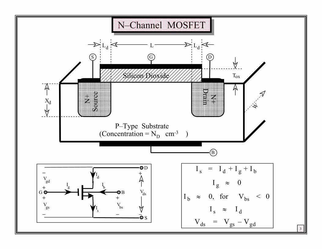
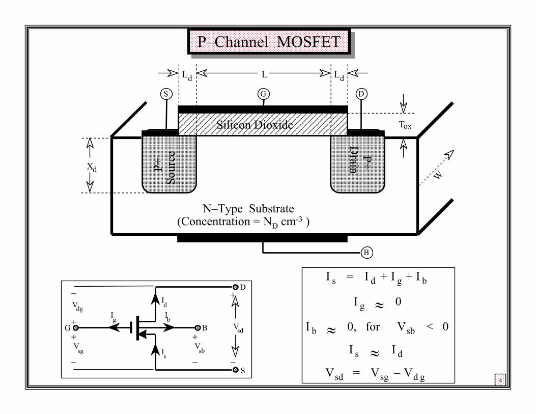
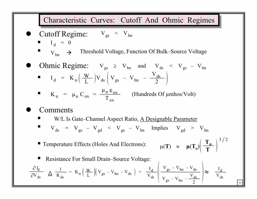
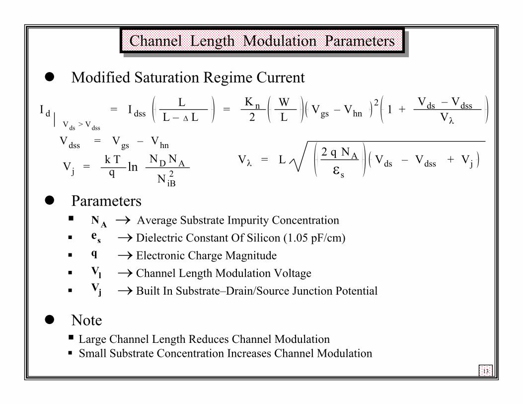
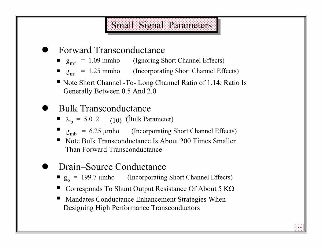
CommentsSquare Law Voltage–Controlled Current SourceDrain Current Shows Negative Temperature CoefficientBecause Of Its Proportionality To MobilityDifferential Current Of Two Matched Devices Is Linear WithDifferential Gate–Source Voltage , Provided Common Mode Gate–Source Voltage Is A Constant
6
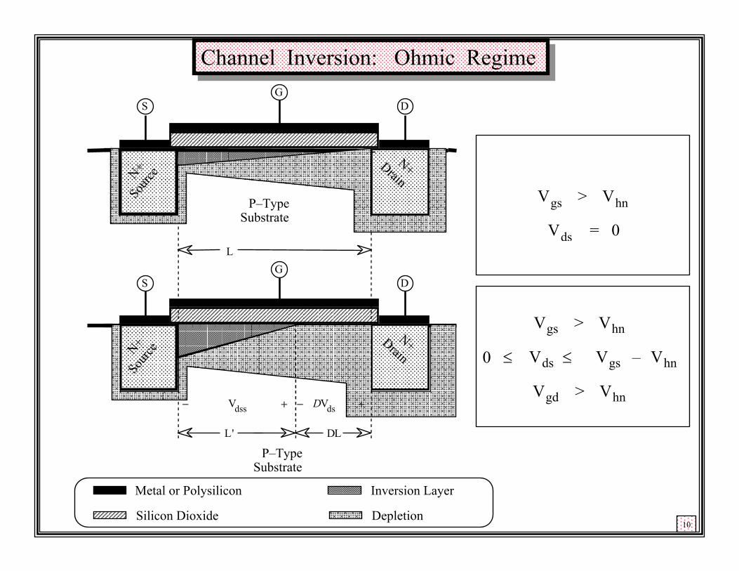
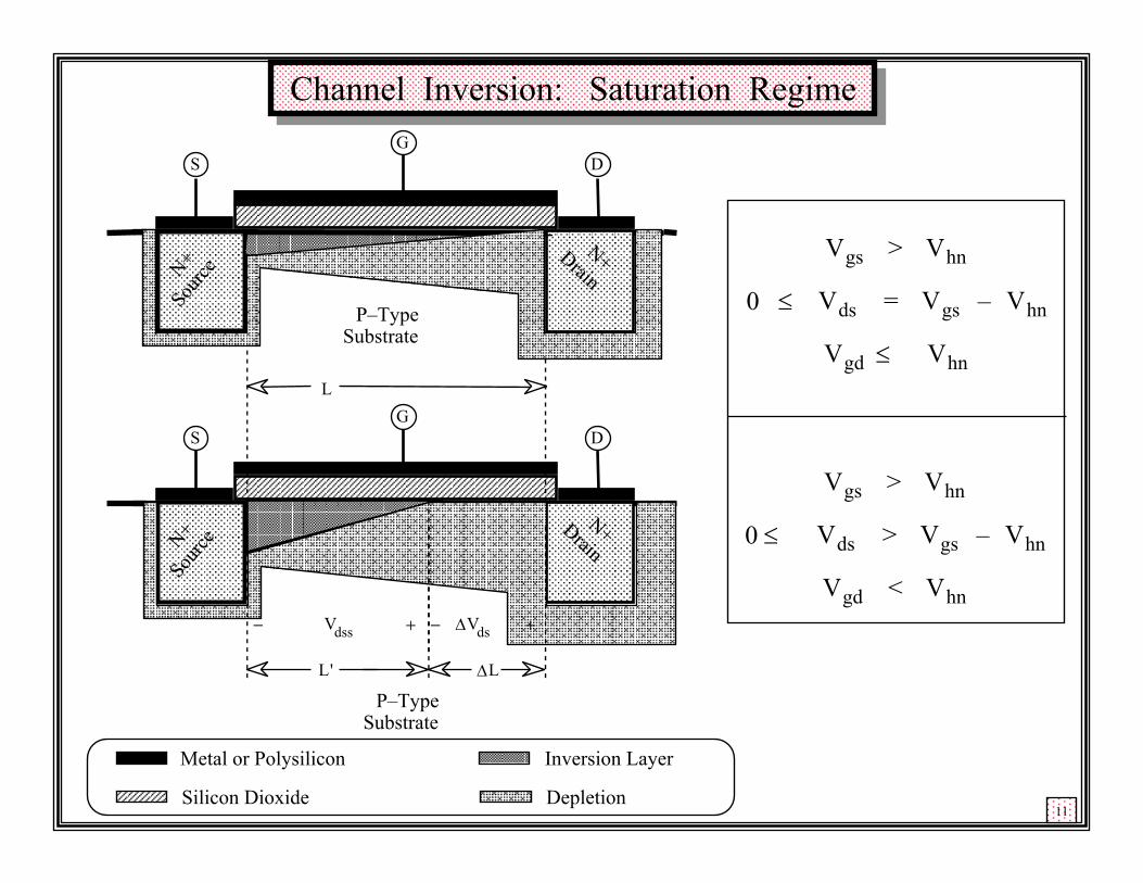
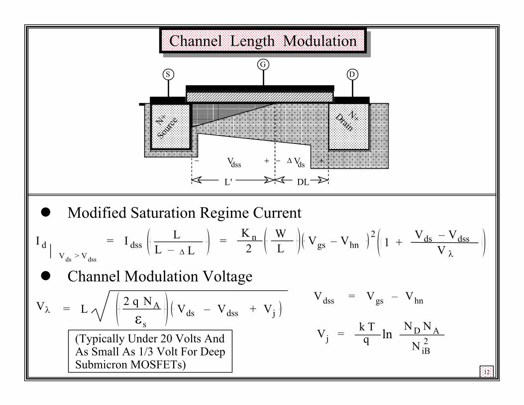
Vgs ≥ Vhn & Vds ≥ Vgs – Vhn
I d = K n 2
W L
Vgs – Vhn 2
Vdss
2
Vgs – Vhn → Drain Saturation Voltage
I dss = K n2
W L Vdss
2 → Drain Saturation Current
I d1 – I d2 = K n 2
W L
Vgs1 – Vhn 2 – Vgs2 – Vhn
2
I d1 – I d2 = K n W L
Vgs1 + Vgs2
2 – Vhn Vgs1 – Vgs2
I d1 – I d2 = K n W L
VCM – Vhn VDM
VDMVCM
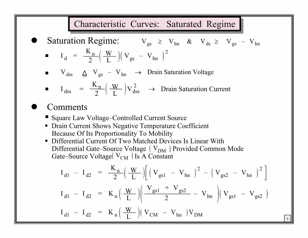
Simple Differential Pair Simple Differential Pair
6a
Vgs1 = VCM + VDM
2
Vgs2 = VCM –
VDM 2
Vgs1 + Vgs2 = 2 VCM
c
R
c
Id2Id1
M1 M2
R
+VDDc
Vo +–
+
–
VDM2
–
+
VDM2
+
–VCM
c Vgs1 – Vgs2 = VDM
I d1 – I d2 = K n W L
VCM – Vhn VDM
Vo = R I d1 – I d2 = K n R W L
VCM – Vhn VDM
Inputs
Response
Note Differential Output Current And Voltage Are Linear With RespectTo Differential Input Voltage Without Invoking Small Signal Approximation
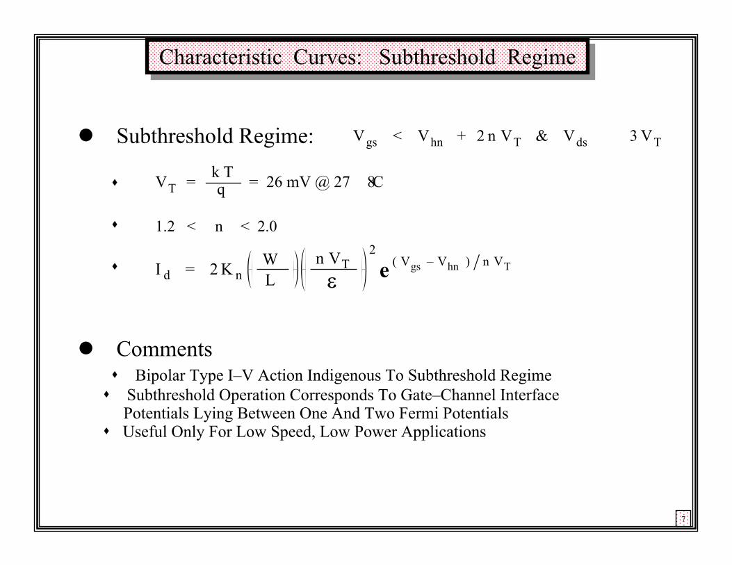
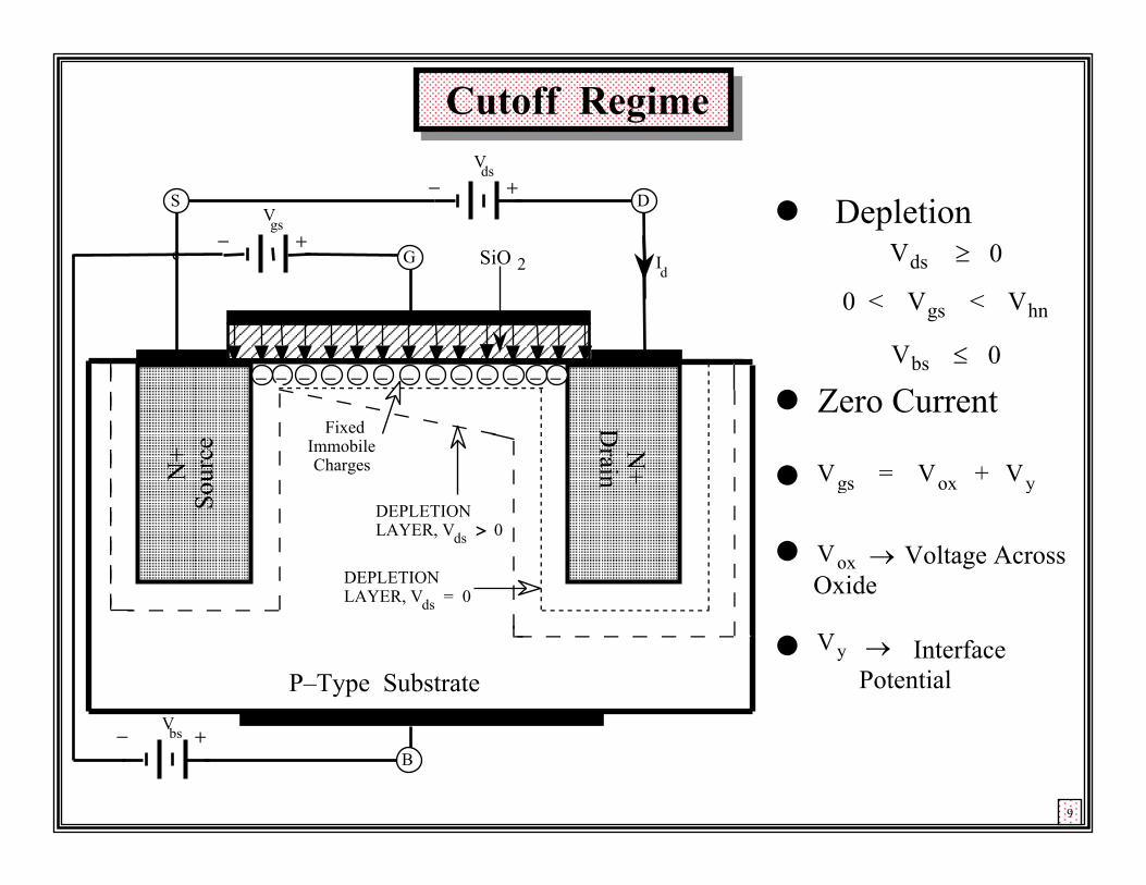
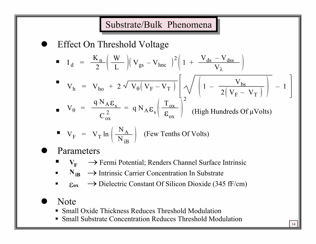
CommentsBipolar Type I–V Action Indigenous To Subthreshold Regime
Subthreshold Operation Corresponds To Gate–Channel InterfacePotentials Lying Between One And Two Fermi PotentialsUseful Only For Low Speed, Low Power Applications
Vgs < Vhn + 2 n VT & Vds 3 VT
VT = k T q = 26 mV @ 27 8C
1.2 < n < 2.0
I d = 2 K nWL
n VTε
2
e ( Vgs – Vhn ) / n VT
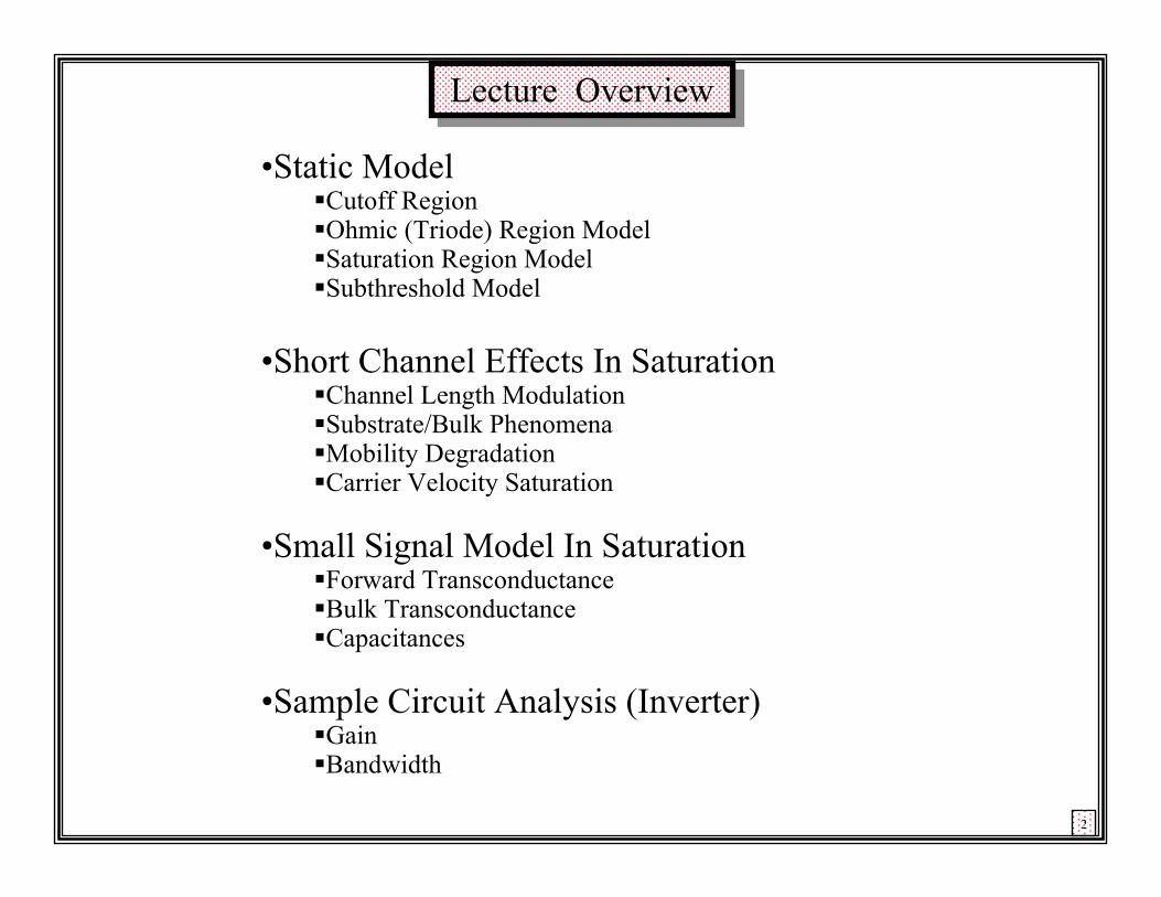
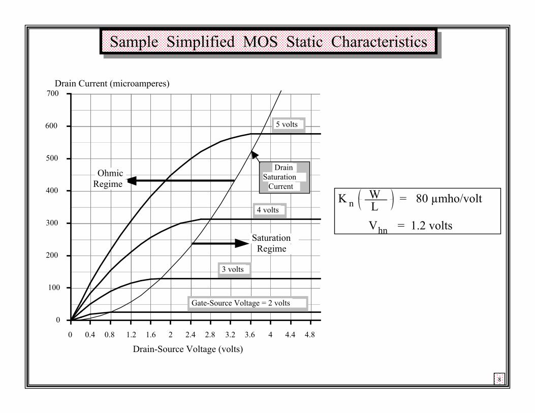
Sample Simplified MOS Static Characteristics Sample Simplified MOS Static Characteristics
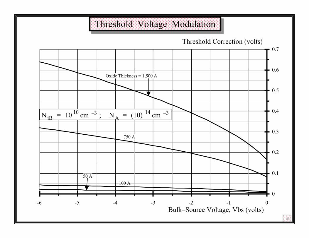
Threshold Voltage Modulation Threshold Voltage Modulation
Threshold Correction (volts)
Bulk–Source Voltage, Vbs (volts)15
0
0.1
0.2
0.3
0.4
0.5
0.6
0.7
-6 -5 -4 -3 -2 -1 0
Oxide Thickness = 1,500 A
750 A
100 A50 A
N iB = 10 10 cm –3 ; N A = (10) 14 cm –3
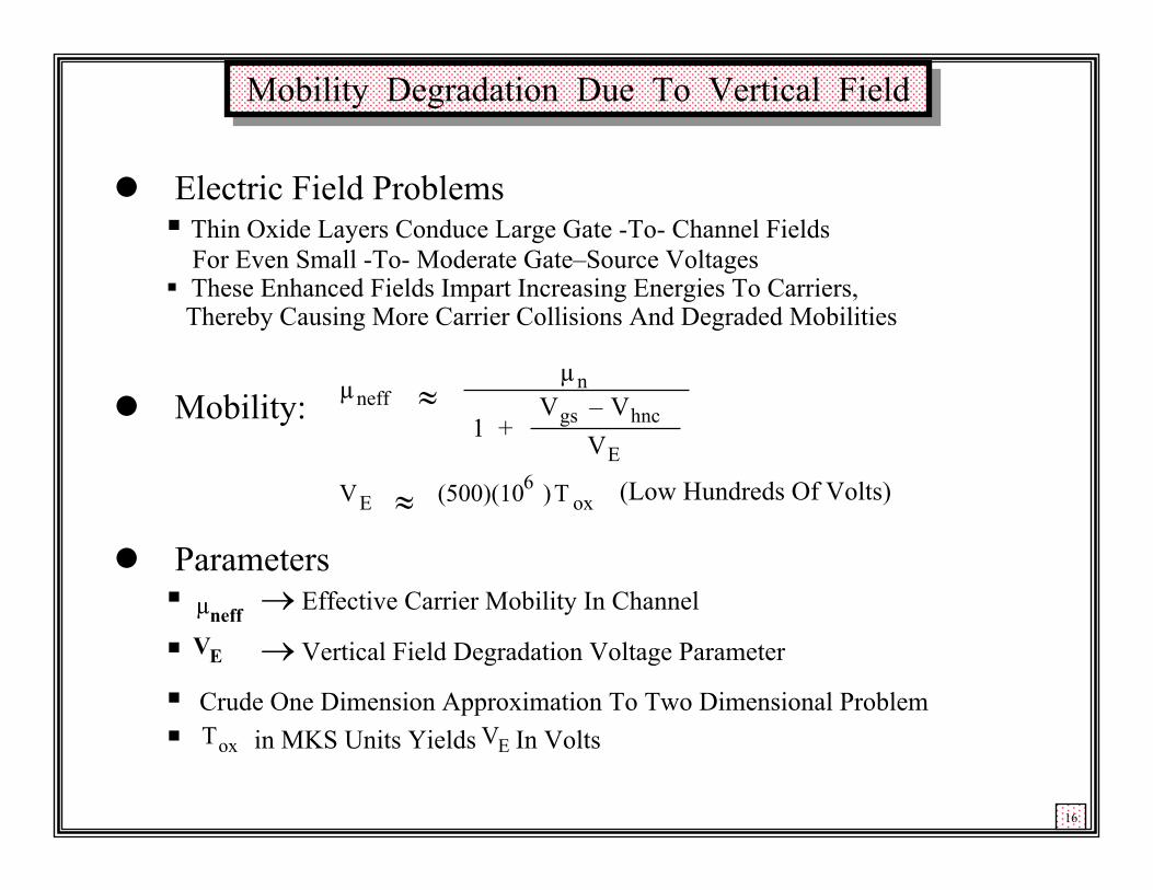
Mobility Degradation Due To Vertical Field Mobility Degradation Due To Vertical Field
16
Electric Field ProblemsThin Oxide Layers Conduce Large Gate -To- Channel FieldsFor Even Small -To- Moderate Gate–Source VoltagesThese Enhanced Fields Impart Increasing Energies To Carriers,Thereby Causing More Carrier Collisions And Degraded Mobilities
Mobility:
Parameters→ Effective Carrier Mobility In Channel
→ Vertical Field Degradation Voltage Parameter
Crude One Dimension Approximation To Two Dimensional Problemin MKS Units Yields In Volts
µneff
Tox VE
VE
µneff ≈µn
1 + Vgs – Vhnc
VE
VE ≈ (500)(106 )T ox (Low Hundreds Of Volts)
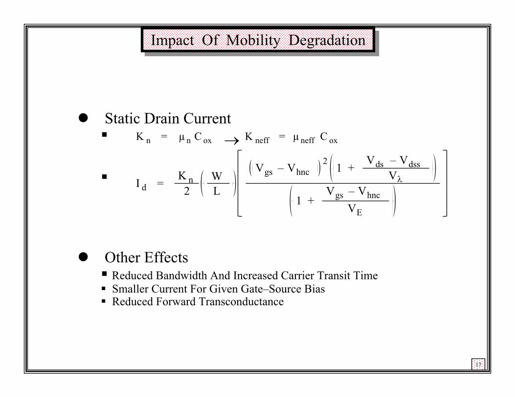
Impact Of Mobility Degradation Impact Of Mobility Degradation
17
Static Drain Current
Other EffectsReduced Bandwidth And Increased Carrier Transit TimeSmaller Current For Given Gate–Source BiasReduced Forward Transconductance
K n = µ n C ox → K neff = µ neff C ox
I d = K n2
WL
Vgs – Vhnc2
1 + Vds – Vdss
Vλ
1 + Vgs – Vhnc
VE
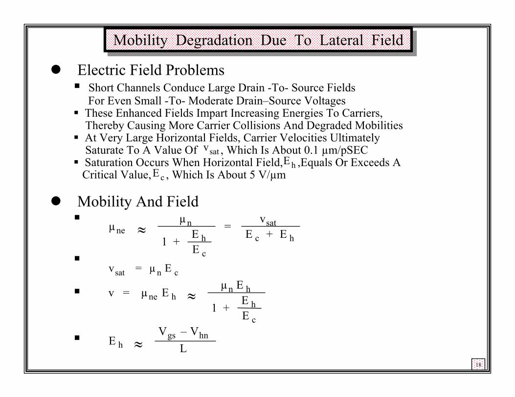
Mobility Degradation Due To Lateral Field Mobility Degradation Due To Lateral Field
18
Electric Field ProblemsShort Channels Conduce Large Drain -To- Source FieldsFor Even Small -To- Moderate Drain–Source Voltages
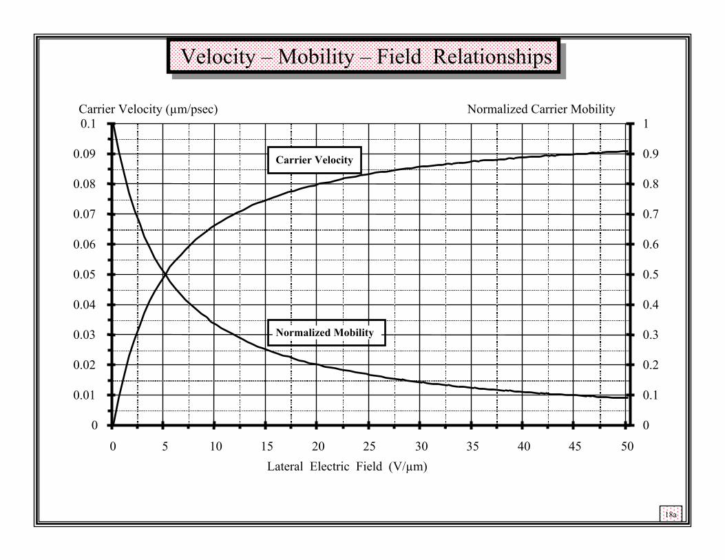
These Enhanced Fields Impart Increasing Energies To Carriers,Thereby Causing More Carrier Collisions And Degraded MobilitiesAt Very Large Horizontal Fields, Carrier Velocities UltimatelySaturate To A Value Of , Which Is About 0.1 µm/pSECSaturation Occurs When Horizontal Field, ,Equals Or Exceeds ACritical Value, , Which Is About 5 V/µm
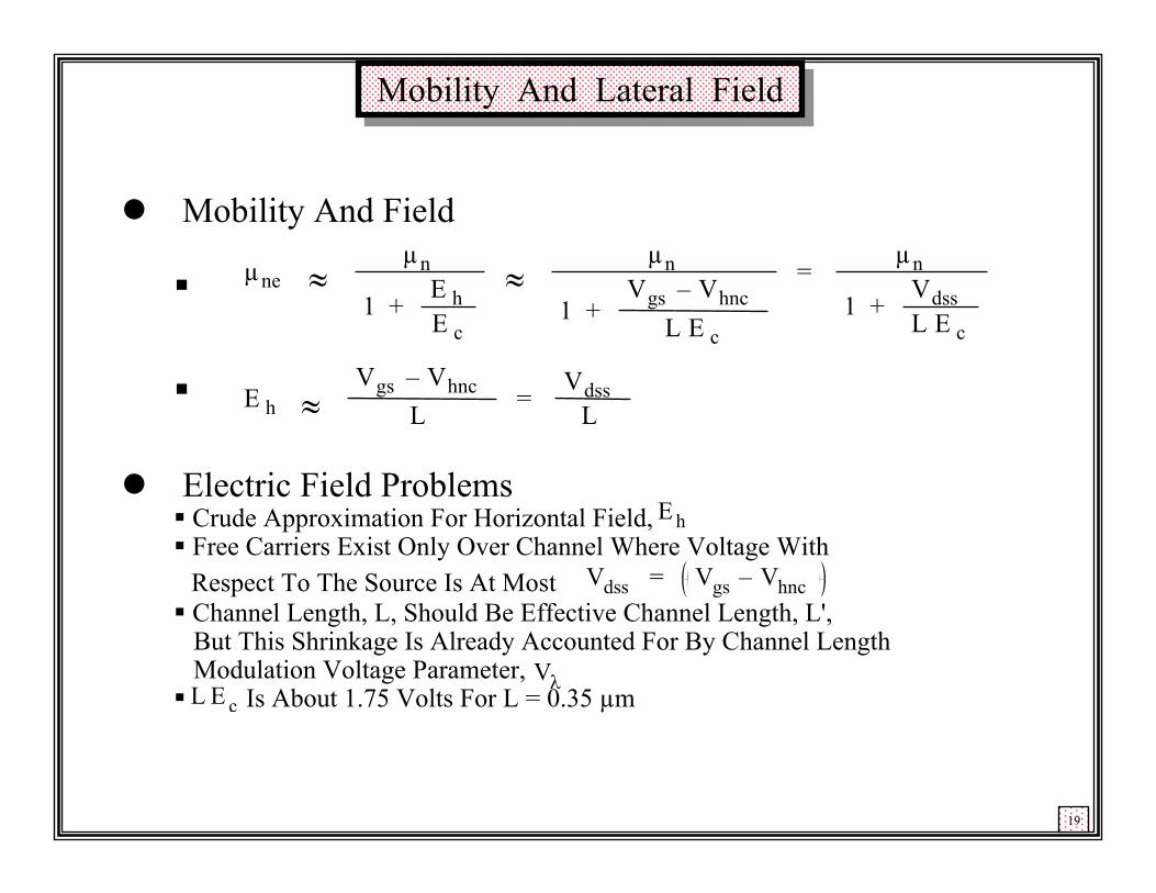
Mobility And Field
vsatE h
Ec
µne ≈µn
1 + E hE c
= vsat
E c + E h
vsat = µ n E c
v = µne E h ≈µn E h
1 + E hE c
E h ≈Vgs – Vhn
L
Velocity – Mobility – Field RelationshipsVelocity – Mobility – Field Relationships
Mobility And Lateral Field Mobility And Lateral Field
19
Mobility And Field
Electric Field ProblemsCrude Approximation For Horizontal Field, Free Carriers Exist Only Over Channel Where Voltage WithRespect To The Source Is At Most Channel Length, L, Should Be Effective Channel Length, L',But This Shrinkage Is Already Accounted For By Channel LengthModulation Voltage Parameter,
Is About 1.75 Volts For L = 0.35 µm
E h
Vλ
E h ≈Vgs – Vhnc
L = VdssL
µne ≈µn
1 + E hE c
≈µn
1 + Vgs – Vhnc
L E c
= µn
1 + VdssL E c
Vdss = Vgs – Vhnc
L E c
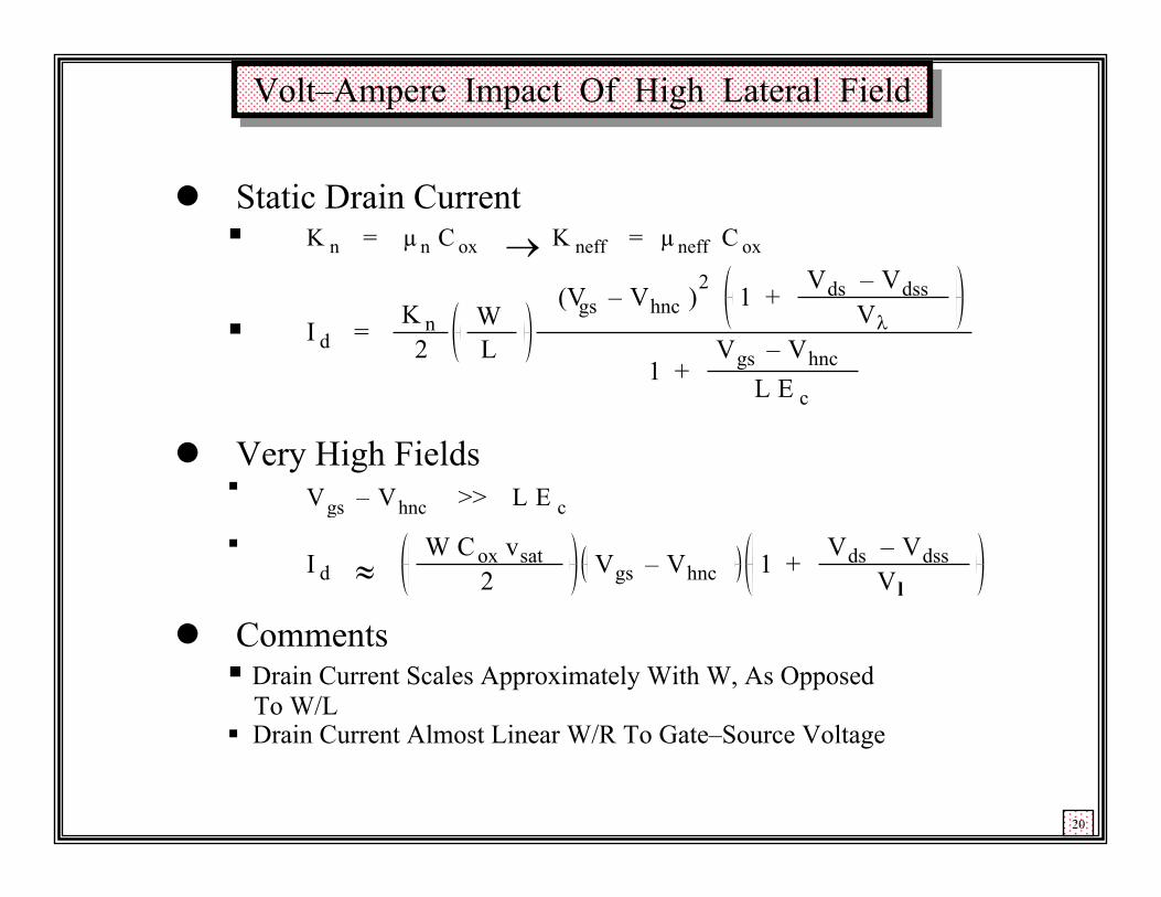
Volt–Ampere Impact Of High Lateral Field Volt–Ampere Impact Of High Lateral Field
Static Drain Current
Very High Fields
CommentsDrain Current Scales Approximately With W, As OpposedTo W/LDrain Current Almost Linear W/R To Gate–Source Voltage
20
K n = µ n C ox → K neff = µ neff C ox
I d = K n2
WL
(Vgs – V )hnc2 1 +
Vds – VdssVλ
1 + Vgs – Vhnc
L E c
Vgs – Vhnc >> L E c
I d ≈W Cox vsat
2 Vgs – Vhnc 1 + Vds – VdssVl
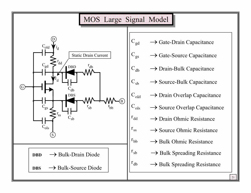
MOS Large Signal Model MOS Large Signal Model
→ Gate-Drain Capacitance
→ Gate-Source Capacitance
→ Drain-Bulk Capacitance
→ Source-Bulk Capacitance
→ Drain Overlap Capacitance
→ Source Overlap Capacitance
DBD → Bulk-Drain Diode
DBS → Bulk-Source Diode21
Cgd
Cgs
Cdb
Csb
Cold
Cols
c c
c
c
c
c
c
DBD
id
B
S
D
G
Id
rdb
DBS
c
Csb
cc cc
Cgd
Cols
Cgs
Cold
Cdb
rbbrsb
rdd
rss → Drain Ohmic Resistancerdd
→ Source Ohmic Resistancerss
→ Bulk Ohmic Resistancerbb
→ Bulk Spreading Resistancersb
→ Bulk Spreading Resistancerdb
Static Drain Current
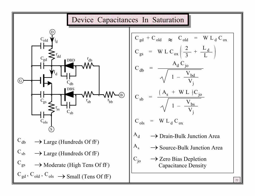
Device Capacitances In Saturation Device Capacitances In Saturation
22
c c
c
c
c
c
c
DBD
id
B
S
D
G
Id
rdb
DBS
c
Csb
cc cc
Cgd
Cols
Cgs
Cold
Cdb
rbbrsb
rdd
rss
→ Drain-Bulk Junction Area
→ Source-Bulk Junction Area
→ Zero Bias Depletion Capacitance Density
Ad
As
Cjo
C gd + C old ≈ C old = W L d C ox
C gs = W L C ox 2
3 +
L d L
C db = Ad C jo
1 – Vbd
Vj
C sb = As + W L C jo
1 – Vbs
Vj
C ols = W L d C ox
→ Large (Hundreds Of fF)Cdb
→ Large (Hundreds Of fF)Csb
→ Moderate (High Tens Of fF)Cgs
Cgd , Cold , Cols → Small (Tens Of fF)
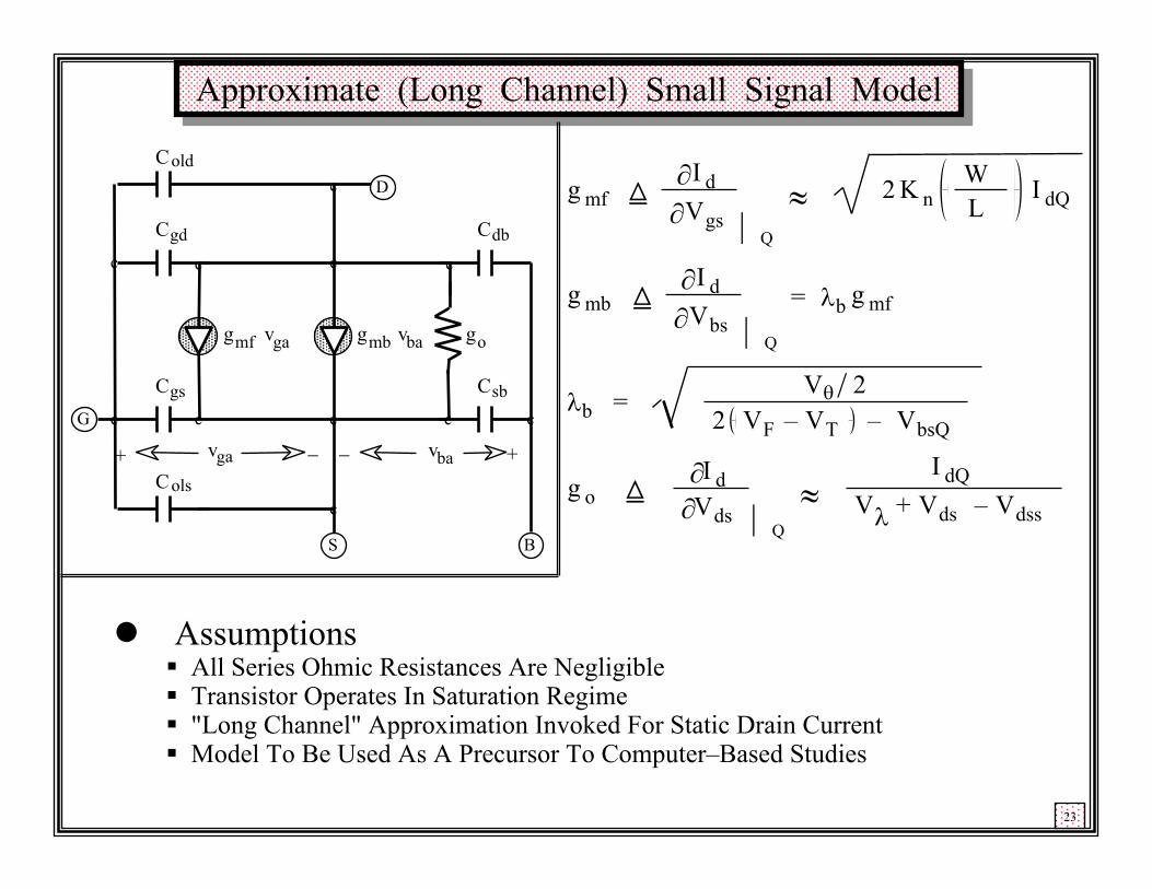
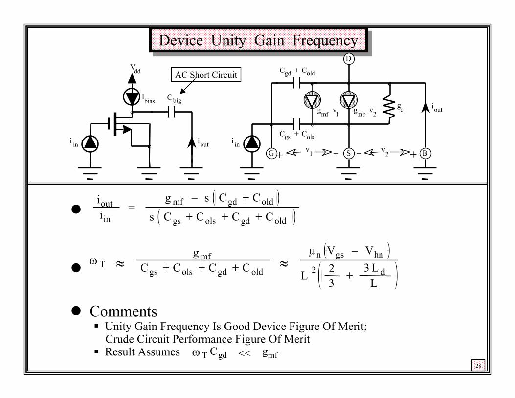
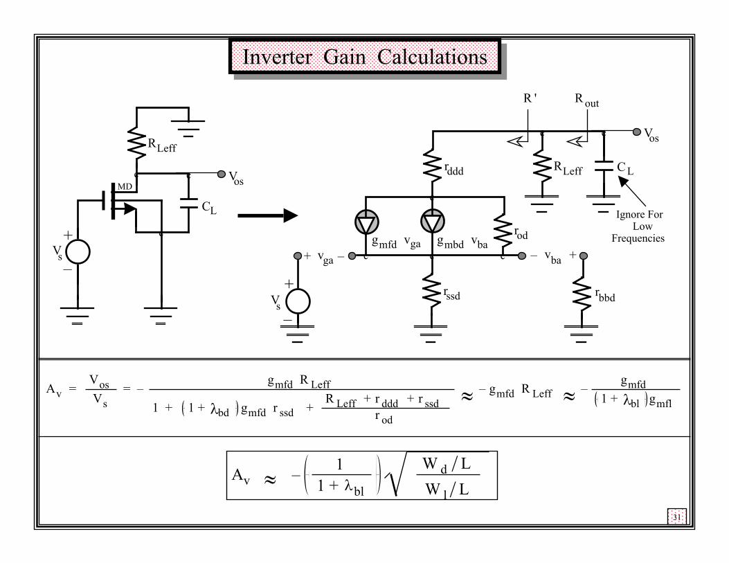
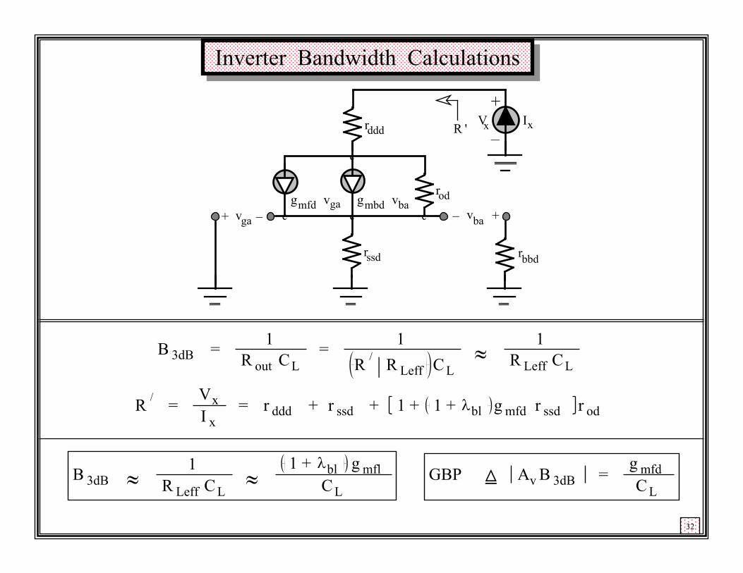
Approximate (Long Channel) Small Signal Model Approximate (Long Channel) Small Signal Model
23
cc
cc
c
B
D
G
gmf vga go
vba +−vga
Cold
+ −
cc
Cgdc
c
gmb vba
Cgs
Cdb
c
Csb
Colsc
S
AssumptionsAll Series Ohmic Resistances Are NegligibleTransistor Operates In Saturation Regime"Long Channel" Approximation Invoked For Static Drain CurrentModel To Be Used As A Precursor To Computer–Based Studies
g mf
2 ∂I d
∂Vgs | Q
≈ 2 K nWL
I dQ
g mb
2 ∂I d
∂Vbs | Q
= λb g mf
λb = Vθ/ 2 2 VF – VT – VbsQ
g o2 ∂I d
∂Vds | Q
≈I dQ
Vλ + Vds – Vdss
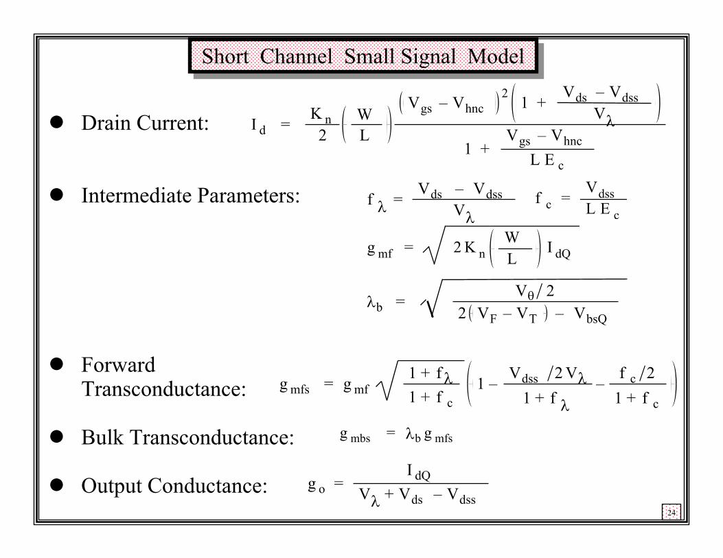
Short Channel Small Signal Model Short Channel Small Signal Model