B.Supmonchai July 5th, 2004 2102-545 Digital ICs 1 Chapter 5 CMOS Inverter Boonchuay Supmonchai Integrated Design Application Research (IDAR) Laboratory July 5, 2004; Revised - June 25, 2005 2102-545 Digital ICs CMOS Inverter 2 B.Supmonchai Goals of This Chapter q Quantification of Design Metrics of an inverter ß Static (or Steady-State) Behavior ß Dynamic (or Transient Response) Behavior ß Energy Efficiency q Optimization of an inverter design q Technology Scaling and its impact on the inverter metrics 2102-545 Digital ICs CMOS Inverter 3 B.Supmonchai Digital Gate Design Metrics: Recap q Cost ß Complexity and Area q Reliability and Robustness ¤ Static Behavior ß Noise Margin, Regenerative Property q Performance ¤ Dynamic Behavior ß Speed (Delay) q Energy Efficiency ß Energy and Power Consumption, Energy-Delay 2102-545 Digital ICs CMOS Inverter 4 B.Supmonchai Why CMOS Inverter? q CMOS because it is the dominating technology of the era. ß High Packing Density ß Relatively Easy Process q Inverter because it is the nucleus of all digital designs. ß Behavior of more intricate structures (logic gates, adders, etc.) can be almost completely derived by extrapolating the results obtained from the inverters.
Transcript
B.Supmonchai July 5th, 2004
2102-545 Digital ICs 1
Chapter 5
CMOS Inverter
Boonchuay SupmonchaiIntegrated Design Application Research (IDAR) Laboratory
July 5, 2004; Revised - June 25, 2005
2102-545 Digital ICs CMOS Inverter 2
B.Supmonchai
Goals of This Chapter
q Quantification of Design Metrics of an inverter
ß Static (or Steady-State) Behavior
ß Dynamic (or Transient Response) Behavior
ß Energy Efficiency
q Optimization of an inverter design
q Technology Scaling and its impact on theinverter metrics
2102-545 Digital ICs CMOS Inverter 3
B.Supmonchai
Digital Gate Design Metrics: Recap
q Cost
ß Complexity and Area
q Reliability and Robustness ¤ Static Behavior
ß Noise Margin, Regenerative Property
q Performance ¤ Dynamic Behavior
ß Speed (Delay)
q Energy Efficiency
ß Energy and Power Consumption, Energy-Delay
2102-545 Digital ICs CMOS Inverter 4
B.Supmonchai
Why CMOS Inverter?
q CMOS because it is the dominating technologyof the era.
ß High Packing Density
ß Relatively Easy Process
q Inverter because it is the nucleus of all digitaldesigns.
ß Behavior of more intricate structures (logic gates,adders, etc.) can be almost completely derived byextrapolating the results obtained from the inverters.
B.Supmonchai July 5th, 2004
2102-545 Digital ICs 2
2102-545 Digital ICs CMOS Inverter 5
B.Supmonchai
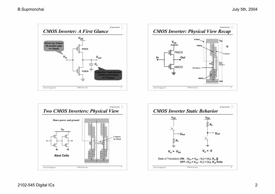
CMOS Inverter: A First Glance
Vin Vout
CL
VDD
PMOS
NMOS
Driven by OutputOf another gate
=> Fanin
Collective CapacitancesOf Wires and Gates
=> Fanout
2102-545 Digital ICs CMOS Inverter 6
B.Supmonchai
Polysilicon
In Out
VDD
GND
PMOS 2l
Metal 1
NMOS
Contacts
N Well
OutIn
VDD
PMOS
NMOS
CMOS Inverter: Physical View Recap
2102-545 Digital ICs CMOS Inverter 7
B.Supmonchai
Connect In Metal
Share power and ground
Two CMOS Inverters: Physical View
VDD
Abut Cells
2102-545 Digital ICs CMOS Inverter 8
B.Supmonchai
VDD
Vin = VDD
Vout
Rn
CMOS Inverter Static BehaviorVDD
Vout
Rp
Vin = 0
State of Transistors ON: |VGT = VGS - VT| > |VT|, Ron Æ • OFF: |VGT = VGS - VT | > |VT|, Roff finite
B.Supmonchai July 5th, 2004
2102-545 Digital ICs 3
2102-545 Digital ICs CMOS Inverter 9
B.SupmonchailGate response time is determined by the time to charge CL through Rp
(discharge CL through Rn)
CMOS Inverter Dynamic Behavior
Charge Discharge
VDD
Rp
Vout
CL
Vin = 0
Low to High
Vin = V DD
CL
VDD
Vout
Rn
High to Low
2102-545 Digital ICs CMOS Inverter 10
B.Supmonchai
CMOS Propertiesq Full rail-to-rail swing
ß High noise margins
ß Logic levels not dependent upon the relative devicesizes => Ratioless
ÿ Transistors can be minimum size
ÿ Regenerative Property
q Low output impedance
ß Large Fan-out (albeit with degraded performance)
ß Typical output resistance in kW range.
2102-545 Digital ICs CMOS Inverter 11
B.Supmonchai
CMOS Properties (2)
q Extremely high input resistance (MOS transistoris near perfect insulator)ß nearly zero steady-state input current
q No direct path between power and ground understeady-state (but there always exists a path withfinite resistance between the output and eitherVDD or GND)ß no static power dissipation
q Propagation delay a function of load capacitanceand resistance of transistors
2102-545 Digital ICs CMOS Inverter 12
B.Supmonchai
NMOS Short Channel I-V Plot Recap
NMOS transistor, 0.25 mm, Ld = 0.25 mm, W/L = 1.5, VDD = 2.5 V, VT = 0.4 V
0
0.5
1
1.5
2
2.5
0 0.5 1 1.5 2 2.5
I D (
A)
VDS (V)
X 10-4
VGS = 1.0 V
VGS = 1.5 V
VGS = 2.0 V
VGS = 2.5 V
Lin
ear
depe
nden
ce
B.Supmonchai July 5th, 2004
2102-545 Digital ICs 4
2102-545 Digital ICs CMOS Inverter 13
B.Supmonchai
PMOS Short Channel I-V Plot Recapl All polarities of all voltages and currents are reversed
-1
-0.8
-0.6
-0.4
-0.2
00-1-2
I D (
A)
VDS (V)
X 10-4
VGS = -1.0 V
VGS = -1.5 V
VGS = -2.0 V
VGS = -2.5 V
PMOS transistor, 0.25 mm, Ld = 0.25 mm, W/L = 1.5, VDD = 2.5 V, VT = -0.4 V
2102-545 Digital ICs CMOS Inverter 14
B.Supmonchai
IDSp = -IDSn
VGSn = Vin ; VGSp = Vin - VDD
VDSn = Vout ; VDSp = Vout - VDD
VGSp = -2.5
VGSp = -1Mirror around x-axis
Vin = VDD + VGSp
IDn = -IDp
Vin = 1.5
Vin = 0
Vin = 1.5
Vin = 0
Horiz. shift over VDD
Vout = VDD + VDSp
Vout
IDn
l NMOS and PMOS VTC must be put into a common coordinateset of Vin, Vout, and IDn
Switching Thresholdq At VM where Vin = Vout, both PMOS and NMOS
transistors are in saturation (since VDS = VGS)
VM ª rVDD/(1 + r) where r = kpVDSATp/knVDSATn
q Switching threshold set by the ratio r, whichcompares the relative driving strengths of thePMOS and NMOS transistors
q Goal: To set VM = VDD/2 (to maximize noisemargins), so r ª 1
†
W L( )p
W L( )n
=kn 'VDSAT ,n VM -VT ,n -VDSAT ,n /2( )
kp 'VDSAT ,p VDD - VM -VT ,p -VDSAT ,p /2( )[ ]
2102-545 Digital ICs CMOS Inverter 19
B.Supmonchai
Switch Threshold Example
q In our generic 0.25 micron CMOS process, using theprocess parameters from Table 3.2, at VDD = 2.5V, and aminimum size NMOS device ((W/L)n of 1.5)
-0.1-30 x 10-6-1-0.4-0.4PMOS
0.06115 x 10-60.630.40.43NMOS
l(V-1)k’(A/V2)VDSAT(V)g(V0.5)VT0(V)
115 x 10-6 0.63 (1.25 – 0.43 – 0.63/2)
-30 x 10-6 -1.0 (1.25 – 0.4 – 1.0/2)x x = 3.5
(W/L)p = 3.5 x 1.5 = 5.25 for a VM of 1.25 V
= (W/L)p
(W/L)n
2102-545 Digital ICs CMOS Inverter 20
B.Supmonchai
Example: Simulated Results
100
1010.8
0.9
1
1.1
1.2
1.3
1.4
1.5
1.6
1.7
1.8
MV (V
)
W p/W n
1.25 V
r = 3.4
Minimum Width-to-Length = 1.5
B.Supmonchai July 5th, 2004
2102-545 Digital ICs 6
2102-545 Digital ICs CMOS Inverter 21
B.Supmonchai
Observations I
q VM is relatively insensitive to variations indevice ratioß Small Variations of the ratio do not significantly
disturb VTC.
ß Common Industry Practice to set Wp smaller than therequirement.
q Increasing the width of the PMOS moves VMtowards VDD
q Increasing the width of the NMOS moves VMtoward GND
2102-545 Digital ICs CMOS Inverter 22
B.Supmonchai
0
1
2
3
VIL VIHVin
Vo
ut
A piece-wise linear approximation of VTC
VOH = VDD
VOL = GND
VIL VIH
Noise Margins: Determining VIH and VIL
NMH = VDD - VIH
NML = VIL - GND
By definition, VIH and VILare where gain
dVout/dVin = -1
So high gain in thetransition region isvery desirable
Slope = g
VM
Gain g = Slope
Approximating: VIH = VM - VM /g VIL = VM + (VDD - VM )/g
2102-545 Digital ICs CMOS Inverter 23
B.Supmonchai
CMOS Voltage Gain
Gain is a strong function of theslopes of the currents in thesaturation region, for Vin = VM
-18
-16
-14
-12
-10
-8
-6
-4
-2
00 0.5 1 1.5 2
Vin
gai
n
q Determined only by technology parameters, especiallychannel length modulation (l). Only designer influencethrough supply voltage and VM (transistor sizing).
2102-545 Digital ICs CMOS Inverter 24
B.Supmonchai
Example: VTC and Noise Marginq For a 0.25mm, (W/L)p/(W/L)n = 3.4, (W/L)n = 1.5
(min size) VDD = 2.5V
VM ª 1.25 V, g = -27.5VIL = 1.2 V, VIH = 1.3 V
NML = NMH = 1.2
q Output resistance fi Sensitivity of gate output with respect to noise
ÿ low-output = 2.4 kWÿhigh-output = 3.3 kWÿ Preferably as low as possible
q First-Order Analysis overestimates the gainß Max. gain only 17 at VM Æ VIL = 1.17V, VIH = 1.33V
q Piecewise Linear Approximation is too overlyoptimisticß Major contributor to deviation from the true gain
q CMOS inverter is a poor analog amplifier!ß One of the major differences between analog and
digital designs is that digital circuits operate in theregions of extreme nonlinearity.ÿ Well-defined and well-separated high and low signals
2102-545 Digital ICs CMOS Inverter 26
B.Supmonchai
0
0.5
1
1.5
2
2.5
0 0.5 1 1.5 2 2.5
Vin(V)
Vou
t(V)
Impact of Process Variation on VTC
No
min
al
Good PMOSBad NMOS
Bad PMOSGood NMOSlProcess variations (mostly) cause a shift in the switching threshold
2102-545 Digital ICs CMOS Inverter 27
B.Supmonchai
Scaling the Supply Voltage
0
0.5
1
1.5
2
2.5
0 0.5 1 1.5 2 2.5
Vin(V)
Vou
t(V)
Reducing VDD improves Gain…
0
0.05
0.1
0.15
0.2
0 0.05 0.1 0.15 0.2
Vin(V)
Vou
t(V)
But it deteriorates for very low VDD
Gain=-1
Practical Lower Bound: VDDmin > 2 to 4 kt /q
2102-545 Digital ICs CMOS Inverter 28
B.Supmonchai
Observations III
q Reducing the supply voltage has a positiveimpact on the energy dissipation …
ß But is also detrimental to the delay of the gate
q DC Characteristic becomes increasinglysensitive to device variations once supply andintrinsic voltages become comparable
q Scaling the supply voltage = reducing the swing
ß Reduce internal noise (e.g., crosstalk)
ß More susceptible to external noise that do not scale
B.Supmonchai July 5th, 2004
2102-545 Digital ICs 8
2102-545 Digital ICs CMOS Inverter 29
B.Supmonchai
CMOS Inverter Dynamic Behaviorq Transient behavior of the gate is determined by
the time it takes to charge and discharge the loadcapacitance, CL, through on-transistorsß Delay is a function of load capacitances and transistor
on-resistances
q Getting CL as small as possible is crucial to therealization of high-performance CMOS circuitsß Transistor Capacitancesß Wire Capacitancesß Fanout
q Wire Resistances also become more important.2102-545 Digital ICs CMOS Inverter 30
B.Supmonchai
VDDVDD
VinVout
M1
M2
M3
M4Cdb2
Cdb1
Cgd12
Cw
Cg4
Cg3
Vout2
Fanout
Interconnect
VoutVin
CL
SimplifiedModel
Fanout
Vout2Vin
Vout
CL
Simplified Model
Intrinsic
Computing the Capacitances
Extrinsic
2102-545 Digital ICs CMOS Inverter 31
B.Supmonchai
Finding Cgd: The Miller Effect
DV
DV
q M1 and M2 are either in cut-off or in saturation.
q The floating gate-drain capacitor is replaced by acapacitance-to-ground (gate-bulk capacitor).
“A capacitor experiencing identical but opposite voltage swingsat both its terminals can be replaced by a capacitor to groundwhose value is two times the original value”
Vin
Vout
Cgd1
M1
Vout
DV
DV
2Cgd1
Vin
M1
2102-545 Digital ICs CMOS Inverter 32
B.Supmonchai
Diffusion Capacitances: Cdb1 and Cdb2
low-to-highhigh-to-low0.25 mmProcess
0.70.590.860.79PMOS
0.810.790.610.57NMOS
KeqswKeqbpKeqswKeqbp
q We can simplify the diffusion capacitancecalculations by using a Keq to linearize thenonlinear capacitor to the value of the junctioncapacitance under zero-bias
Ceq = Keq Cj0
B.Supmonchai July 5th, 2004
2102-545 Digital ICs 9
2102-545 Digital ICs CMOS Inverter 33
B.Supmonchai
Extrinsic Capacitances: Cg3 and Cg4
q Simplification of the actual situation
ß Assumes all the components of Cgate are between Vout
and GND (or VDD)
ß Assumes the channel capacitances of the loadinggates are constant
q The extrinsic, or fan-out, capacitance is the totalgate capacitance of the loading gates M3 and M4.
AD = Drain Area PD = Drain Perimeter AS = Source AreaPS = Source Perimeter
Minimum Drawn Length
2102-545 Digital ICs CMOS Inverter 35
B.Supmonchai
Example: Components of CL (0.25 mm)
6.06.1ÂCL
0.120.12from extractionCw
2.282.28(2 Cgd0p)Wp + CoxWpLpCg4
0.760.76(2 Cgd0n)Wn + CoxWnLnCg3
1.151.5KeqbppADpCj + KeqswpPDpCjswCdb2
0.900.66KeqbpnADnCj + KeqswnPDnCjswCdb1
0.610.612 Cgd0p WpCgd2
0.230.232 Cgd0n WnCgd1
Value (fF)
LÆHValue (fF)
HÆLExpressionC Term
2102-545 Digital ICs CMOS Inverter 36
B.Supmonchai
Wiring Capacitance
q The wiring capacitance depends upon the lengthand width of the connecting wires and is afunction of the fan-out from the driving gate andthe number of fan-out gates.
q Wiring capacitance is growing in importancewith the scaling of technology.
B.Supmonchai July 5th, 2004
2102-545 Digital ICs 10
2102-545 Digital ICs CMOS Inverter 37
B.Supmonchai
Inverter Propagation Delay
Charge
VDD
Rp
Vout
CL
Vin = 0
Low to High
Discharge
Vin = V DD
CL
VDD
Vout
Rn
High to Low
“Propagation delay is proportional to the time-constant of thenetwork formed by the on-resistance and the load capacitance”
q To equalize rise and fall times make the on-resistance of theNMOS and PMOS approximately equal.
ÿ where tp0 = 0.69 Req Cint is the intrinsic (unloaded) delayof the gate
q Widening both PMOS and NMOS by a factor S reducesReq by an identical factor (Req = Rref/S), but raises theintrinsic capacitance by the same factor (Cint = SCiref)
Impact of Fanout on Delayq Extrinsic capacitance, Cext, is a function of the
fanout of the gateß the larger the fanout, the larger the external load.
q First determine the input loading effect of theinverter. Both Cg and Cint are proportional to the gatesizing, so Cint = gCg is independent of gate sizing and
tp = tp0 (1 + Cext/ gCg) = tp0 (1 + f /g)
q The delay of an inverter is a function of the ratiobetween its external load capacitance and its inputgate capacitance: the effective fan-out f
f = Cext/Cg
2102-545 Digital ICs CMOS Inverter 47
B.Supmonchai
q Goal: to minimize the delay through an inverter chain
q If CL is givenß How should the inverters be sized?ß How many stages are needed to minimize the delay?
2102-545 Digital ICs CMOS Inverter 48
B.Supmonchai
Sizing the Inverters in the Chainq The optimum size of each inverter is the geometric mean
of its neighbors – meaning that if each inverter is sizedup by the same factor f wrt the preceding gate, it willhave the same effective fan-out and the same delay
†
f = CL Cg,1N = FN
where F represents the overall effective fan-out of thecircuit (F = CL/Cg,1)
q The minimum delay through the inverter chain is
†
t p = Ntp0 1+ FN /g( )ÿ The relationship between tp and F is linear for one inverter,
square root for two, etc.
B.Supmonchai July 5th, 2004
2102-545 Digital ICs 13
2102-545 Digital ICs CMOS Inverter 49
B.Supmonchai
Example: Inverter Chain Sizing
q CL/Cg,1 has to be evenly distributed over N = 3 inverters
CL/Cg,1 = 8/1
f =
In Out
CL = 8 Cg,1Cg,1
1 f = 2 f2 = 4
3÷8 = 2
2102-545 Digital ICs CMOS Inverter 50
B.Supmonchai
Determining N: Optimal Number of Inverters
q What is the optimal value for N given F (=fN) ?ß If the number of stages is too large, the intrinsic delay of the
stages becomes dominate
ß If the number of stages is too small, the effective fan-out of eachstage becomes dominate
q The optimum N is found by differentiating the minimumdelay expression divided by the number of stages andsetting the result to 0, giving
ß For g = 0 (ignoring self-loading) N = ln (F) and the effective-fan outbecomes f = e = 2.71828
ß For g = 1 (the typical case) the optimum effective fan-out (taperingfactor) turns out to be close to 3.6
N Ng + ÷F - ( ÷F lnF)/N = 0
2102-545 Digital ICs CMOS Inverter 51
B.Supmonchai
Optimum Effective Fan-Out
q Choosing f larger than optimum has little effect ondelay and reduces the number of stages (and area).ß Common practice to use f = 4 (for g = 1)ß But too many stages has a substantial negative impact on delay
2.5
3
3.5
4
4.5
5
0 0.5 1 1.5 2 2.5 3
g
Fo
pt
0
1
2
3
4
5
6
7
1 1.5 2 2.5 3 3.5 4 4.5 5
f
Norm
ali
zed
Dela
y
2102-545 Digital ICs CMOS Inverter 52
B.Supmonchai
Example: Inverter (Buffer) StagingN f tp
1 64 65
CL = 64 Cg,1Cg,1 = 1
1 2.8 8 22.6
CL = 64 Cg,1Cg,1 = 1
1 4 16
CL = 64 Cg,1Cg,1 = 1
1 8
CL = 64 Cg,1Cg,1 = 1
1
2 8 18
3 4 15
4 2.8 15.3
B.Supmonchai July 5th, 2004
2102-545 Digital ICs 14
2102-545 Digital ICs CMOS Inverter 53
B.Supmonchai
Impact of Buffer Staging for Large CL
q Impressive speed-ups with optimized cascadedinverter chain for very large capacitive loads.
33.120210,00110,000
24.86510011,000
16.522101100
8.38.31110
Opt.InverterChain
TwoStageChain
UnbufferedF
(g = 1)
2102-545 Digital ICs CMOS Inverter 54
B.Supmonchai
36
38
40
42
44
46
48
50
52
54
0 20 40 60 80
tS(psec)
t p(p
sec)
Input Signal Rise/Fall Timeq In reality, the input signal changes gradually (and both
PMOS and NMOS conduct for a brief time). This affectsthe current available for charging/discharging CL andimpacts propagation delay.
for a minimum-size inverter with a fan-out of a single gate
! ts is due to the limiteddriving capability of thepreceding gate
ts = input signal slope
2102-545 Digital ICs CMOS Inverter 55
B.Supmonchai
Design Challengeq A gate is never designed in isolation: its performance is
affected by both the fan-out and the driving strength ofthe gate(s) feeding its inputs. (Revised tp expression)
tip = tistep + h ti-1step (h ª 0.25)
q Keep signal rise times smaller than or equal to the gatepropagation delays.ß good for performance
ß good for power consumption
q Keeping rise and fall times of the signals small and ofapproximately equal values is one of the major challengesin high-performance designs - slope engineering.
2102-545 Digital ICs CMOS Inverter 56
B.Supmonchai
Delay with Long Interconnectq When gates are farther apart, wire capacitance and resis-
ß Ideally zero for static CMOS but in the real world..
ß Leakage Current Lossÿ Diodes and Transistors constantly losing charge
q Dynamic Power Consumption
ß Charging/Discharging Capacitancesÿ Major Source of Power Dissipation in CMOS Circuits
ß Direct-Path Current Lossÿ Short circuit between Power Rail during Switching
2102-545 Digital ICs CMOS Inverter 58
B.Supmonchai
Pdyn = Energy/cycle * fclk
Vin Vout
CL
VDD
Dynamic Power Consumption
iVDD(t)
Energy Supplied/Cycle =
†
iVDD (t)VDDdt0
•
Ú = CL * VDD2
Energy Stored/Cycle =
†
iVDD (t)vout (t)dt0
•
Ú = CL * VDD2 / 2
= CL * VDD2 * fclk
2102-545 Digital ICs CMOS Inverter 59
B.Supmonchai
Switching Activity
q Power dissipation does not depend on the size ofthe devices but depends on how often the circuit isswitched.ß Switching Activity ≡ frequency of energy-consuming
transition = f 0Æ1
Pdyn = CL * VDD2 * f 0Æ1
= CL * VDD2 * P0Æ1 * fclk
= Ceff * VDD2 * fclk
Clock
Gate output
Effective Capacitance Ceff = AverageCapacitance Switched per clock cycle
P0Æ1 = 0.25, f0Æ1 = fclk / 4
2102-545 Digital ICs CMOS Inverter 61
B.Supmonchai
Lowering Dynamic Power
Pdyn = CL VDD2 P0Æ1 f
Clock frequency:Increasing…
Quadratic EffectLowering Physical Capacitance
Activity factor:How often, on average,do gates switch?
Supply Voltage:Has been dropping withsuccessive generations
Capacitance:Function of fan-out, wirelength, transistor sizes
Reduction can be obtained only at Logicand Architectural Abstraction Levels
B.Supmonchai July 5th, 2004
2102-545 Digital ICs 16
2102-545 Digital ICs CMOS Inverter 62
B.Supmonchai
Finite slope of the input signal causes a direct currentpath between VDD and GND for a short period of time
during switching when both the NMOS and PMOStransistors are conducting (active).
Short Circuit Power Consumption
CL
Vin Vout
VDD
Isc
tsc
2102-545 Digital ICs CMOS Inverter 63
B.Supmonchai
Esc = tsc VDD Ipeak P0Æ1
Psc = tsc VDD Ipeak f0Æ1
Short Circuit Currents Determinates
q tsc = Duration of the slope of the input signal
q Ipeak determined byß the saturation current of the PMOS and NMOS transistors
which depend on their sizes, process technology, temperature,etc.
ß strong function of the ratio between input and output slopesÿ a function of CL
2102-545 Digital ICs CMOS Inverter 64
B.Supmonchai
Isc ª 0 Isc ª Imax
Large capacitive load Small capacitive load
Impact of CL on Psc
Vin Vout
CL
VDD
Vin Vout
CL
VDD
Output fall time significantlylarger than input rise time.
Output fall time substantiallysmaller than input rise time.
2102-545 Digital ICs CMOS Inverter 65
B.Supmonchai
Ipeak as a Function of CL
-0.5
0
0.5
1
1.5
2
2.5
0 2 4 6I p
eak (
A)
time (sec)x 10-10
x 10-4
CL = 20 fF
CL = 100 fF
CL = 500 fF
500 psec input slope
Short circuit dissipationis minimized bymatching the rise/falltimes of the input andoutput signals - slopeengineering.
When load capacitanceis small, Ipeak is large.
B.Supmonchai July 5th, 2004
2102-545 Digital ICs 17
2102-545 Digital ICs CMOS Inverter 66
B.Supmonchai
Psc as a Function of Rise/Fall Times
normalized wrt zero inputrise-time dissipation
When load capacitanceis small (tsin/tsout > 2 forVDD > 2V) the power isdominated by Psc
If VDD < VTn + |VTp| thenPsc is eliminated sinceboth devices are neveron at the same time.
q All leakages increase exponentially with temperature
ß Junction leakage doubles every 9C
q Sub-threshold current becomes more concern in vDSM
ß The closer the threshold voltage to zero, the larger theleakage current at VGS = 0V (when NMOS off)
2102-545 Digital ICs CMOS Inverter 68
B.Supmonchai
Leakage as a Function of VT
1.E-12
1.E-10
1.E-08
1.E-06
1.E-04
1.E-02
0 0.2 0.4 0.6 0.8 1
VGS (V)
I D (
A)
VT=0.4VVT=0.1V
q Continued scaling of supply voltage and the subsequentscaling of threshold voltage will make sub-thresholdconduction a dominant component of power dissipation.
q An 90mV/decade VTroll-off - so each255mV increase inVT gives 3 orders ofmagnitude reductionin leakage (butadversely affectsperformance)
2102-545 Digital ICs CMOS Inverter 69
B.Supmonchai
80
0.25 V
13,000
920/400
0.08 mm
24 Å
1.2 V
CL013HS
52
0.29 V
1,800
860/370
0.11 mm
29 Å
1.5 V
CL015HS
42 Å42 Å42 Å42 ÅTox (effective)
43142230FET Perf.(GHz)
0.40 V0.73 V0.63 V0.42 VVTn
3000.151.6020Ioff (leakage)(rA/mm)
780/360320/130500/180600/260IDSat (n/p)(mA/mm)
0.13 mm0.18 mm0.16 mm0.16 mmLgate
2 V1.8 V1.8 V1.8 VVdd
CL018HS
CL018ULP
CL018LP
CL018G
TSMC Processes Leakage and VTFrom MPR, June 2000, pp. 19 – Performance of various TSMC processes(G generic, LP low power, ULP ultra low power, HS high speed)
B.Supmonchai July 5th, 2004
2102-545 Digital ICs 18
2102-545 Digital ICs CMOS Inverter 70
B.Supmonchai
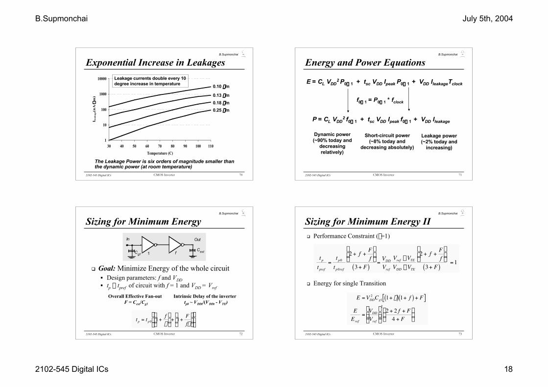
Exponential Increase in Leakages
1
10
100
1000
10000
30 40 50 60 70 80 90 100 110
Temperature (C)
I lea
ka
ge(
nA
/ mm
)
0.10 mm
0.13 mm
0.18 mm
0.25 mm
Leakage currents double every 10degree increase in temperature
The Leakage Power is six orders of magnitude smaller thanthe dynamic power (at room temperature)
ß EDP is the average energy consumed multiplied by thecomputation time required
ß Takes into account that one can trade increased delayfor lower energy/operation (e.g., via supply voltagescaling that increases delay, but decreases energyconsumption)