Date post: | 06-Mar-2018 |
Category: |
Documents |
Upload: | hoangduong |
View: | 229 times |
Download: | 4 times |
IS61WV25616EDALL
Integrated Silicon Solution, Inc.- www.issi.com 1 Rev. A1
02/06/2017
256Kx16 HIGH SPEED ASYNCHRONOUS CMOS STATIC RAM with ECC
KEY FEATURES
High-speed access time: 20ns
Single power supply – 1.65V-2.2V VDD
Low Standby Current:1.5mA (typical)
Fully static operation: no clock or refresh required
Data control
Three state outputs
Industrial and Automotive temperature support
Lead-free available Error Detection and Correction
FUNCTIONAL BLOCK DIAGRAM
COLUMN I/O
WE#UB#
OE#
LB#
CONTROL
CIRCUIT
I/O
DATA
CIRCUIT
DECODER
VDD
VSS
A0 – A17
I/O0 – I/O7
I/O8 – I/O15
Memory
Upper IO
Array
256Kx8
ECC
Array
256Kx4
Column I/O
8 4 8 4
ECC
Array
256Kx4
ECC
ECC
8
8
12
12
Memory
Lower IO
Array
256Kx8
CS#
DESCRIPTION The ISSI IS61WV25616EDALL are high-speed, low power,
4M bit static RAMs organized as 256K words by 16 bits. It
is fabricated using ISSI's high-performance CMOS
technology and implemented ECC function to improve
reliability.
When CS# is HIGH (deselected), the device assumes a
standby mode at which the power dissipation can be
reduced down with CMOS input levels.
Easy memory expansion is provided by using Chip Enable
and Output Enable inputs. The active LOW Write Enable
(WE#) controls both writing and reading of the memory.
A data byte allows Upper Byte (UB#) and Lower Byte (LB#)
access.
The IS61WV25616EDALL are packaged in the JEDEC
standard 48-pin mini BGA (6mm x 8mm), and 44-pin TSOP
(TYPE II)
Copyright © 2017 Integrated Silicon Solution, Inc. All rights reserved. ISSI reserves the right to make changes to this specification and its products at any time without notice. ISSI assumes no liability arising out of the application or use of any information, products or services described herein. Customers are advised to obtain the latest version of this device specification before relying on any published information and before placing orders for products. Integrated Silicon Solution, Inc. does not recommend the use of any of its products in life support applications where the failure or malfunction of the product can reasonably be expected to cause failure of the life support system or to significantly affect its safety or effectiveness. Products are not authorized for use in such applications unless Integrated Silicon Solution, Inc. receives written assurance to its satisfaction, that: a.) the risk of injury or damage has been minimized; b.) the user assume all such risks; and c.) potential liability of Integrated Silicon Solution, Inc is adequately protected under the circumstances
FEBRUARY 2017
IS61WV25616EDALL
Integrated Silicon Solution, Inc.- www.issi.com 2 Rev. A1
02/06/2017
PIN CONFIGURATIONS 48-Pin mini BGA(6mm x 8mm)
LB# A0OE# A1 A2 NC
I/O8 A3UB# A4 CS# I/O0
I/O9 A5I/O10 A6 I/O1 I/O2
VSS A17I/O11 A7 I/O3 VDD
VDD NCI/O12 A16 I/O4 VSS
I/O14 A14I/O13 A15 I/O5 I/O6
I/O15 A12NC A13 WE# I/O7
NC A9A8 A10 A11 NC
1 2 3 4 5 6
A
B
C
D
E
F
G
H
44-Pin TSOP-II
A0
A1
A2
A3
A4
CS#
I/O0
I/O1
I/O2
I/O3
VDD
VSS
I/O4
I/O5
I/O6
I/O7
WE#
A5
A6
A7
A8
A9
A17
A16
A15
OE#
UB#
LB#
I/O15
I/O14
I/O13
I/O12
VDD
VSS
I/O11
I/O10
I/O9
I/O8
NC
A14
A13
A12
A11
A10
1
2
3
4
5
6
7
8
9
10
12
11
13
14
15
16
32
31
30
29
28
27
26
25
24
23
21
22
20
19
18
17
42
41
40
39
38
37
36
35
34
33
44
43
PIN DESCRIPTIONS
A0-A17 Address Inputs
I/O0-I/O15 Data Inputs/Outputs
CS# Chip Enable Input
OE# Output Enable Input
WE# Write Enable Input
LB# Lower-byte Control (I/O0-I/O7)
UB# Upper-byte Control (I/O8-I/O15)
NC No Connection
VDD Power
VSS Ground
IS61WV25616EDALL
Integrated Silicon Solution, Inc.- www.issi.com 3 Rev. A1
02/06/2017
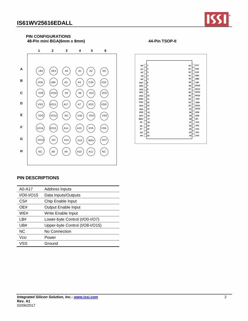
FUNCTION DESCRIPTION SRAM is one of random access memories. Each byte or word has an address and can be accessed randomly. SRAM has various modes supported. Each function is described below with Truth Table.
STANDBY MODE Device enters standby mode when deselected (CS# HIGH). The input and output pins (I/O0-15) are placed in a high impedance state. The current consumption in this mode will be ISB1, or ISB2.
WRITE MODE Write operation issues with Chip Select (CS#) Low and Write Enable (WE#) Low. The input and output pins (I/O0-15) are in data input mode. Output buffers are closed during this time even if OE# is Low. UB# and LB# enables a byte write feature. By enabling LB# Low, data from I/O pins (I/O0 through I/O7) are written into the location specified on the address pins. And with UB# being Low, data from I/O pins (I/O8 through I/O15) are written into the location.
READ MODE Read operation issues with Chip Select (CS#) Low and Write Enable (WE#) High. When OE# is Low, output buffer turns on to make data output. Any input to I/O pins during READ mode is not permitted. UB# and LB# enables a byte read feature. By enabling LB# Low, data from memory appears on I/O0-7. And with UB# being Low, data from memory appears on I/O8-15. In the READ mode, output buffers can be turned off by pulling OE# High. In this mode, internal device operates as READ but I/Os are in a high impedance state. Since device is in READ mode, active current is used. TRUTH TABLE
Mode CS# WE# OE# LB# UB# I/O0-I/O7 I/O8-I/O15 VDD Current
Not Selected H X X X X High-Z High-Z ISB1, ISB2
Output Disabled L H H L X High-Z High-Z
ICC,ICC1 L X X H H High-Z High-Z
Read
L H L L H DOUT High-Z
ICC,ICC1 L H L H L High-Z DOUT
L H L L L DOUT DOUT
Write
L L X L H DIN High-Z
ICC,ICC1 L L X H L High-Z DIN
L L X L L DIN DIN
IS61WV25616EDALL
Integrated Silicon Solution, Inc.- www.issi.com 4 Rev. A1
02/06/2017
ABSOLUTE MAXIMUM RATINGS(1) Symbol Parameter Value Unit
Vterm Terminal Voltage with Respect to VSS –0.5 to VDD + 0.5V V
VDD VDD Related to VSS –0.3 to 4.0 V
tStg Storage Temperature –65 to +150 C
PT Power Dissipation 1.0 W
Notes:
1. Stress greater than those listed under ABSOLUTE MAXIMUM RATINGS may cause permanent damage to the device. This is a stress rating only and functional operation of the device at these or any other conditions above those indicated in the operational sections of this specification is not implied. Exposure to absolute maximum rating conditions for extended periods may affect reliability.
.
PIN CAPACITANCE (1)
Parameter Symbol Test Condition Max Units
Input capacitance CIN TA = 25°C, f = 1 MHz, VDD = VDD(typ)
6 pF
DQ capacitance (IO0–IO15) CI/O 8 pF
Note: 1. These parameters are guaranteed by design and tested by a sample basis only.
OPERATING RANGE(1)
Range Ambient Temperature
PART NUMBER SPEED (MAX) VDD
Commercial 0C to +70C IS61WV25616EDALL
20 ns 1.65V – 2.2V
Industrial -40C to +85C 20 ns 1.65V – 2.2V
Note:
1. Full device AC operation assumes a 100 µs ramp time from 0 to VDD(min) and 200 µs wait time after VDD stabilization.
THERMAL CHARACTERISTICS (1)
Parameter Symbol Rating Units
Thermal resistance from junction to ambient (airflow = 1m/s) RθJA TBD °C/W
Thermal resistance from junction to pins RθJB TBD °C/W
Thermal resistance from junction to case RθJC TBD °C/W Note: 1. These parameters are guaranteed by design and tested by a sample basis only.
IS61WV25616EDALL
Integrated Silicon Solution, Inc.- www.issi.com 5 Rev. A1
02/06/2017
AC TEST CONDITIONS (OVER THE OPERATING RANGE)
Parameter Unit (1.65V~2.2V)
Input Pulse Level 0V to VDD
Input Rise and Fall Time 1.5 ns
Output Timing Reference Level 0.9V
R1 (ohm) 13500
R2 (ohm) 10800
VTM (V) 1.8V
Output Load Conditions Refer to Figure 1 and 2
OUTPUT LOAD CONDITIONS FIGURES
Output
Zo = 50 ohm50 ohm
30 pF,
Including
jig
and scope
VDD/2
R1
R2
VTM
OUTPUT5pF,
Including
jig
and scope
R1
R2
VTM
OUTPUT5pF,
Including
jig
and scope
FIGURE 1 FIGURE 2
IS61WV25616EDALL
Integrated Silicon Solution, Inc.- www.issi.com 6 Rev. A1
02/06/2017
DC ELECTRICAL CHARACTERISTICS IS61(64)WV25616EEBLL DC ELECTRICAL CHARACTERISTICS-I (OVER THE OPERATING RANGE) VDD = 1.65V – 2.2V
Symbol Parameter Test Conditions Min. Max. Unit
VOH Output HIGH Voltage IOH = -0.1 mA 1.4 — V
VOL Output LOW Voltage IOL = 0.1 mA — 0.2 V
VIH(1) Input HIGH Voltage 1.4 VDD + 0.2 V
VIL(1) Input LOW Voltage –0.2 0.4 V
ILI Input Leakage GND < VIN < VDD –1 1 µA
ILO Output Leakage GND < VIN < VDD, Output Disabled –1 1 µA
Notes:
1. VILL(min) = -1.0V AC (pulse width < 20ns). Not 100% tested. 2. VIHH (max) = VDD + 1.0V AC (pulse width < 20ns). Not 100% tested.
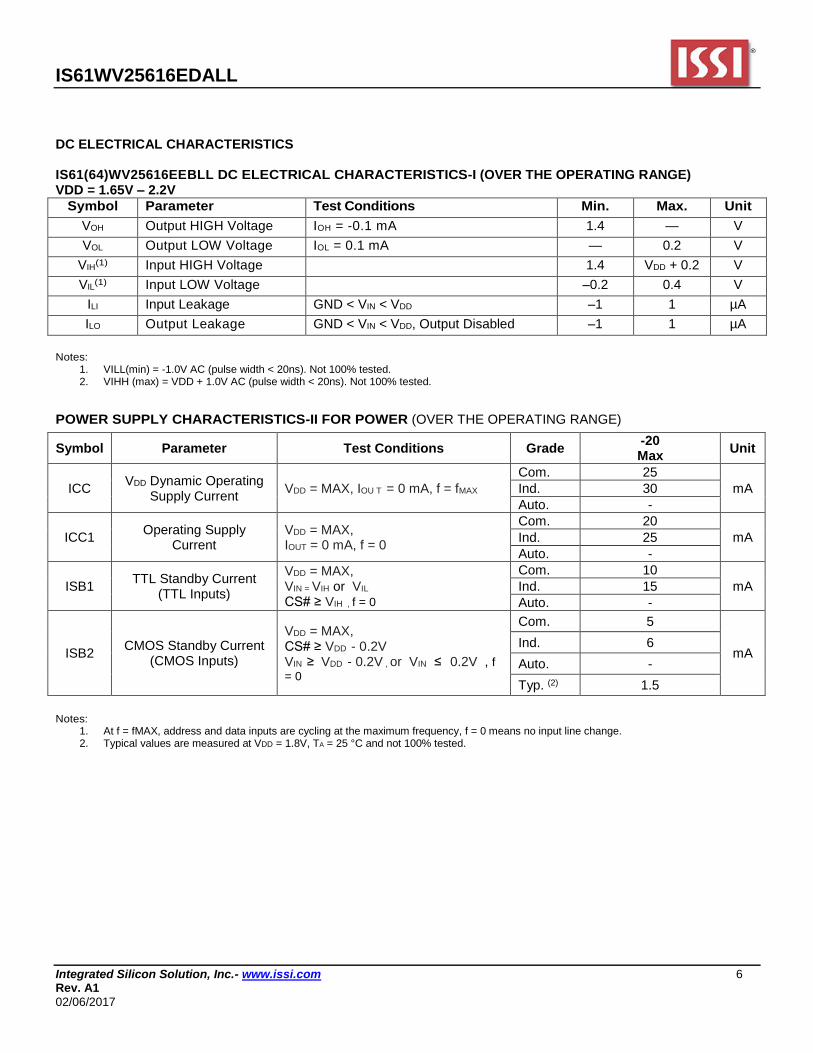
POWER SUPPLY CHARACTERISTICS-II FOR POWER (OVER THE OPERATING RANGE)
Symbol Parameter Test Conditions Grade -20 Max
Unit
ICC VDD Dynamic Operating
Supply Current VDD = MAX, IOU T = 0 mA, f = fMAX
Com. 25
mA Ind. 30
Auto. -
ICC1 Operating Supply
Current VDD = MAX, IOUT = 0 mA, f = 0
Com. 20
mA Ind. 25
Auto. -
ISB1 TTL Standby Current
(TTL Inputs)
VDD = MAX, VIN = VIH or VIL
CS# ≥ VIH , f = 0
Com. 10
mA Ind. 15
Auto. -
ISB2 CMOS Standby Current
(CMOS Inputs)
VDD = MAX, CS# ≥ VDD - 0.2V
VIN ≥ VDD - 0.2V , or VIN ≤ 0.2V , f = 0
Com. 5
mA Ind. 6
Auto. -
Typ. (2) 1.5
Notes:
1. At f = fMAX, address and data inputs are cycling at the maximum frequency, f = 0 means no input line change. 2. Typical values are measured at VDD = 1.8V, TA = 25 °C and not 100% tested.
IS61WV25616EDALL
Integrated Silicon Solution, Inc.- www.issi.com 7 Rev. A1
02/06/2017
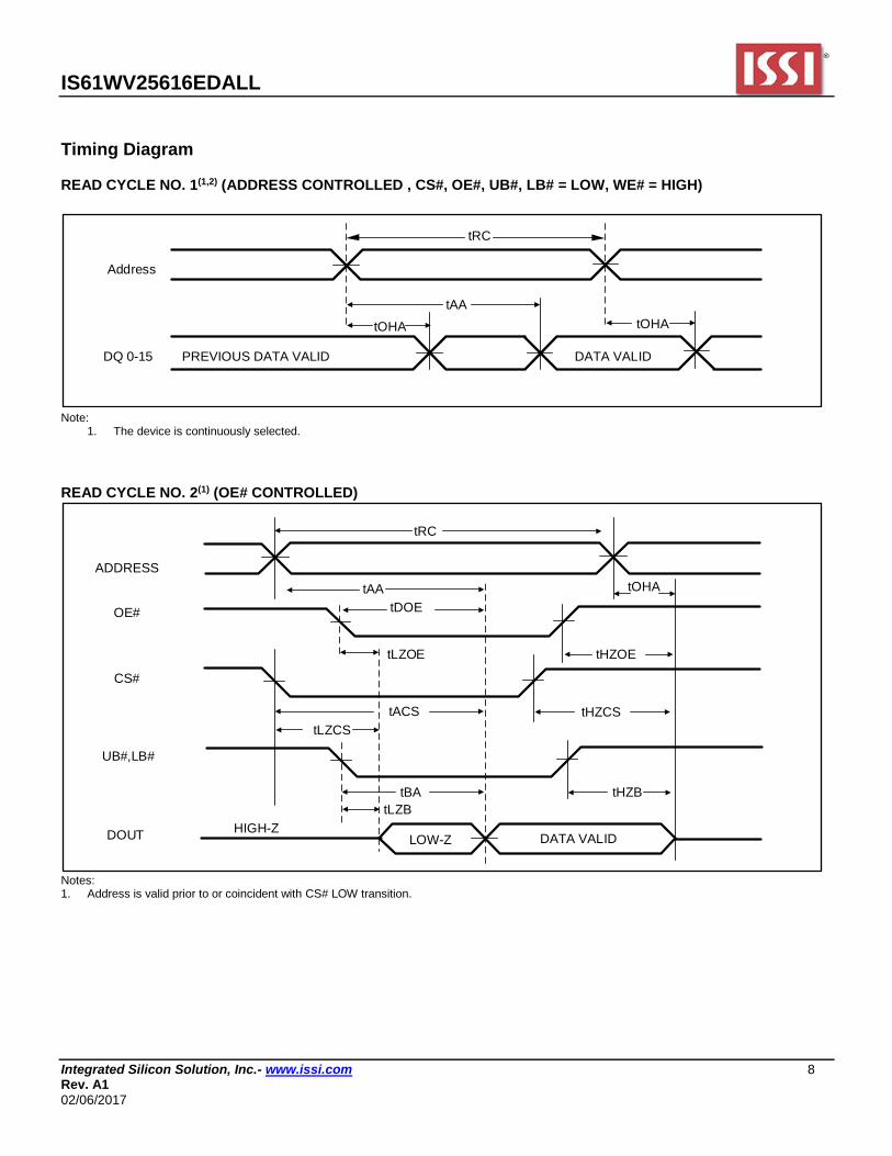
AC CHARACTERISTICS (OVER OPERATING RANGE) READ CYCLE AC CHARACTERISTICS
Parameter Symbol -20(1)
unit notes Min Max
Read Cycle Time tRC 20 - ns
Address Access Time tAA - 20 ns
Output Hold Time tOHA 2.5 - ns
CS# Access Time tACE - 20 ns
OE# Access Time tDOE - 8 ns
OE# to High-Z Output tHZOE 0 8 ns 2
OE# to Low-Z Output tLZOE 0 - ns 2
CS# to High-Z Output tHZCE 0 8 ns 2
CS# to Low-Z Output tLZCE 3 - ns 2
UB#, LB# Access Time tBA - 8 ns
UB#, LB# to High-Z Output tHZB 0 8 ns 2
UB#, LB# to Low-Z Output tLZB 0 - ns 2 Notes:
1. Test conditions assume signal transition times of 3 ns or less, timing reference levels of VDD/2, and output loading specified in Figure 1. 2. Tested with the load in Figure 2. Transition is measured ±500 mV from steady-state voltage. Not 100% tested.
IS61WV25616EDALL
Integrated Silicon Solution, Inc.- www.issi.com 8 Rev. A1
02/06/2017
Timing Diagram
READ CYCLE NO. 1(1,2) (ADDRESS CONTROLLED , CS#, OE#, UB#, LB# = LOW, WE# = HIGH)
tRC
Address
DQ 0-15
tOHA tOHA
tAA
PREVIOUS DATA VALID DATA VALID
Note:
1. The device is continuously selected.
READ CYCLE NO. 2(1) (OE# CONTROLLED)
OE#
CS#
DOUT
tAA
ADDRESS
tRC
tOHA
tDOE
tLZOE
tACS
tLZCS
tHZOE
tHZCS
HIGH-ZDATA VALID
tLZB
tHZBtBA
UB#,LB#
LOW-Z
Notes: 1. Address is valid prior to or coincident with CS# LOW transition.
IS61WV25616EDALL
Integrated Silicon Solution, Inc.- www.issi.com 9 Rev. A1
02/06/2017
WRITE CYCLE AC CHARACTERISTICS
Parameter Symbol -20(1)
unit notes Min Max
Write Cycle Time tWC 20 - ns
CS# to Write End tSCS 12 - ns
Address Setup Time to Write End tAW 12 - ns
UB#,LB# to Write End tPWB 12 - ns
Address Hold from Write End tHA 0 - ns
Address Setup Time tSA 0 - ns
WE# Pulse Width tPWE1 12 - ns
WE# Pulse Width (OE# = LOW) tPWE2 17 - ns 2
Data Setup to Write End tSD 9 - ns
Data Hold from Write End tHD 0 - ns
WE# LOW to High-Z Output tHZWE - 9 ns
WE# HIGH to Low-Z Output tLZWE 3 - ns Notes:
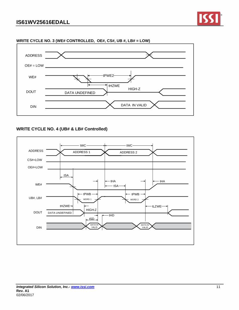
1 Test conditions assume signal transition times of 3 ns or less, timing reference levels of VDD/2, and output loading specified in Figure 1. 2 Tested with the load in Figure 2. Transition is measured ±500 mV from steady-state voltage. Not 100% tested. 3 The internal write time is defined by the overlap of CS# = LOW, UB# or LB# = LOW, and WE# = LOW. All signals must be in valid states to
initiate a Write, but anyone can go inactive to terminate the Write. The Data Input Setup and Hold timing are referenced to the rising or falling edge of the signal that terminates the write.
4 If OE# is LOW during write cycle, (WE# controlled, CS# = UB# = LB# = LOW), the minimum Write cycle time for write cycle NO.3 is the sum of tHZWE and tSD
IS61WV25616EDALL
Integrated Silicon Solution, Inc.- www.issi.com 10 Rev. A1
02/06/2017
Timing Diagram
WRITE CYCLE NO. 1(1) (WE# CONTROLLED, OE# = HIGH OR LOW)
ADDRESS
CS#
WE#
DOUT
DIN
tWC
tHA
tAWtPWE1
tPWE2
tSA
tHZWE tLZWE
tSD tHD
DATA IN VALID
DATA UNDEFINEDHIGH-Z
UB#,LB# tPBW
tSCS
Notes: 1. tHZWE is based on the assumption when tSA=0nS after READ operation. Actual DOUT for tHZWE may not appear if OE# goes high
before Write Cycle.
WRITE CYCLE NO. 2 (WE# CONTROLLED)
tWC
tSCS tHA
tAW
tPWE1
tSA
tHZWE tLZWEHIGHZ
tSD tHD
DATA UNDEFINED
DATA IN VALID
ADDRESS
CS#
WE#
DOUT
DIN
OE#
tPWB
UB#,LB#
IS61WV25616EDALL
Integrated Silicon Solution, Inc.- www.issi.com 11 Rev. A1
02/06/2017
WRITE CYCLE NO. 3 (WE# CONTROLLED, OE#, CS#, UB #, LB# = LOW)
tPWE2
HIGH-ZDATA UNDEFINED
DATA IN VALID
ADDRESS
WE#
DOUT
DIN
OE# = LOW
tHZWE
WRITE CYCLE NO. 4 (UB# & LB# Controlled)
ADDRESS
CS#=LOW
WE#
DOUT
DIN
tSA
tHZWE
tPWB
tHA
DATA IN
VALID
ADDRESS 1 ADDRESS 2
tWC tWC
tPWB
DATA IN
VALID
DATA UNDEFINEDtHD
tSD
HIGH-ZtLZWE
WORD 1 WORD 2UB#, LB#
tSA
tHA
OE#=LOW
IS61WV25616EDALL
Integrated Silicon Solution, Inc.- www.issi.com 12 Rev. A1
02/06/2017
DATA RETENTION CHARACTERISTICS
Symbol Parameter Test Condition OPTION Min. Typ.(2) Max. Unit
VDR VDD for Data Retention
See Data Retention Waveform 1.2 - - V
IDR Data Retention Current
VDD = MAX, CS# ≥ VDD – 0.2V, VIN ≥ VDD - 0.2V, or VIN ≤ 0.2V
Com. - 0.5 5 mA
Ind. - - 6
tSDR Data Retention Setup Time
See Data Retention Waveform 0 - -
ns
tRDR Recovery Time See Data Retention Waveform tRC - - ns
Notes: 1. If CS# >VDD–0.2V, all other inputs including UB# and LB# must meet this condition.
2. Typical values are measured at VDD= 1.8V, TA = 25℃ and not 100% tested.
DATA RETENTION WAVEFORM (CS# CONTROLLED)
GND
CS#
VDR
VDD
CS# > VDD – 0.2V
Data Retention ModetSDR tRDR
IS61WV25616EDALL
Integrated Silicon Solution, Inc.- www.issi.com 13 Rev. A1
02/06/2017
ORDERING INFORMATION
Industrial Range: –40°C to +85°C
Speed (ns) Order Part No. Package
20 IS61WV25616EDALL-20BI mini BGA (6mm x 8mm)
20 IS61WV25616EDALL-20BLI mini BGA (6mm x 8mm), Lead-free
20 IS61WV25616EDALL-20TLI TSOP (Type II), Lead-free
IS61WV25616EDALL
Integrated Silicon Solution, Inc.- www.issi.com 14 Rev. A1
02/06/2017
PACKAGE INFORMATION
IS61WV25616EDALL
Integrated Silicon Solution, Inc.- www.issi.com 15 Rev. A1
02/06/2017