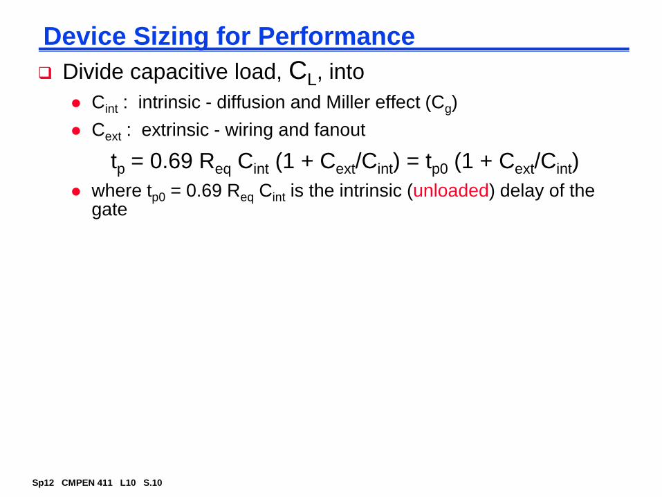
where tp0 = 0.69 Req Cint is the intrinsic (unloaded) delay of the gate
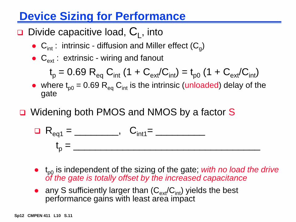
Widening both PMOS and NMOS by a factor S
Req1 = ________, Cint1= _________
tp = __________________________________
tp0 is independent of the sizing of the gate; with no load the drive of the gate is totally offset by the increased capacitance
any S sufficiently larger than (Cext/Cint) yields the best performance gains with least area impact
Sp12 CMPEN 411 L10 S.12
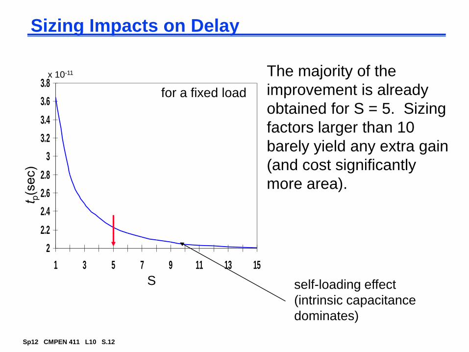
Sizing Impacts on Delay
2
2.2
2.4
2.6
2.8
3
3.2
3.4
3.6
3.8
1 3 5 7 9 11 13 15
S
x 10-11 The majority of the
improvement is already
obtained for S = 5. Sizing
factors larger than 10
barely yield any extra gain
(and cost significantly
more area).
for a fixed load
self-loading effect
(intrinsic capacitance
dominates)
Sp12 CMPEN 411 L10 S.13
Impact of Fanout on Delay
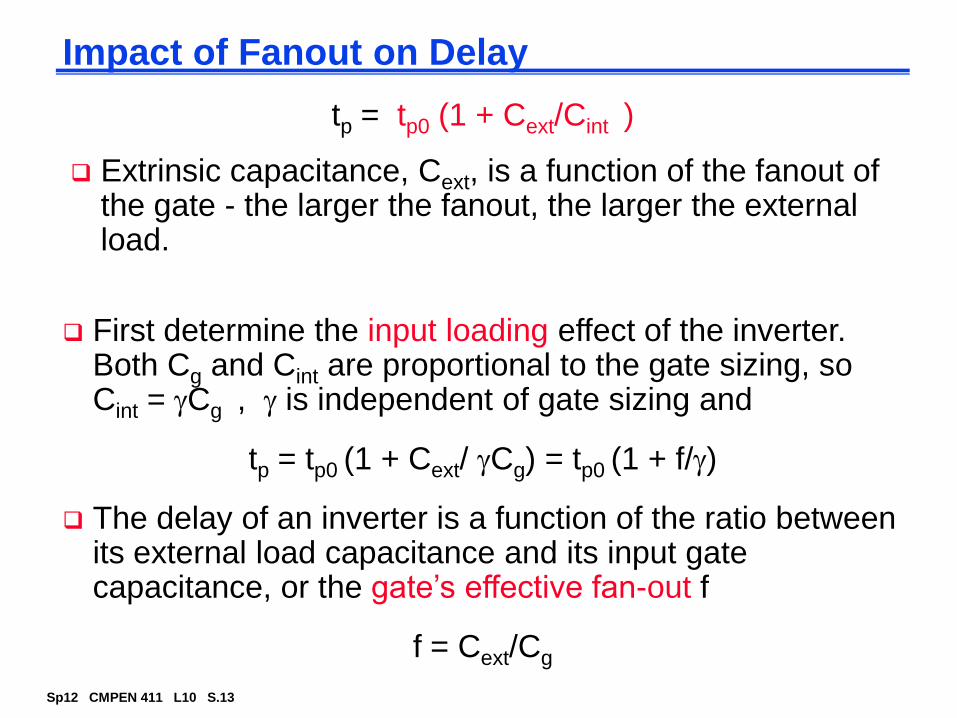
Extrinsic capacitance, Cext, is a function of the fanout of the gate - the larger the fanout, the larger the external load.
First determine the input loading effect of the inverter. Both Cg and Cint are proportional to the gate sizing, so Cint = Cg , is independent of gate sizing and
tp = tp0 (1 + Cext/ Cg) = tp0 (1 + f/)
The delay of an inverter is a function of the ratio between its external load capacitance and its input gate capacitance, or the gate’s effective fan-out f
f = Cext/Cg
tp = tp0 (1 + Cext/Cint )
Sp12 CMPEN 411 L10 S.14
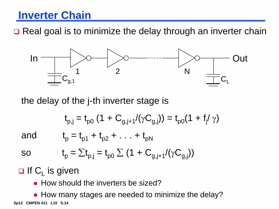
Inverter Chain
If CL is given
How should the inverters be sized?
How many stages are needed to minimize the delay?
In Out
CL
Real goal is to minimize the delay through an inverter chain
the delay of the j-th inverter stage is
tp,j = tp0 (1 + Cg,j+1/(Cg,j)) = tp0(1 + fj/ )
and tp = tp1 + tp2 + . . . + tpN
so tp = tp,j = tp0 (1 + Cg,j+1/(Cg,j))
Cg,1
1 2 N
Sp12 CMPEN 411 L10 S.15
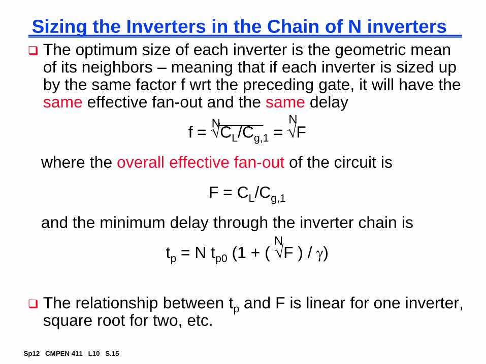
Sizing the Inverters in the Chain of N inverters
The optimum size of each inverter is the geometric mean of its neighbors – meaning that if each inverter is sized up by the same factor f wrt the preceding gate, it will have the same effective fan-out and the same delay
f = CL/Cg,1 = F
where the overall effective fan-out of the circuit is
F = CL/Cg,1
and the minimum delay through the inverter chain is
tp = N tp0 (1 + ( F ) / )
The relationship between tp and F is linear for one inverter, square root for two, etc.
N N
N
Sp12 CMPEN 411 L10 S.16
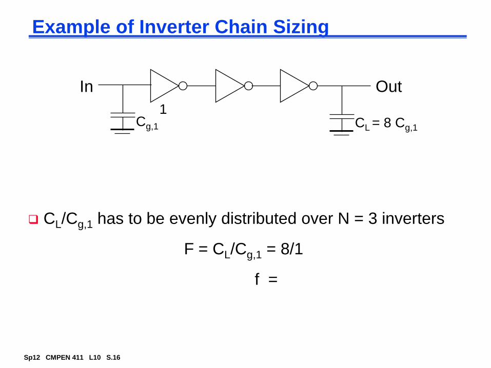
Example of Inverter Chain Sizing
CL/Cg,1 has to be evenly distributed over N = 3 inverters
F = CL/Cg,1 = 8/1
f =
In Out
CL = 8 Cg,1Cg,1
1
Sp12 CMPEN 411 L10 S.17
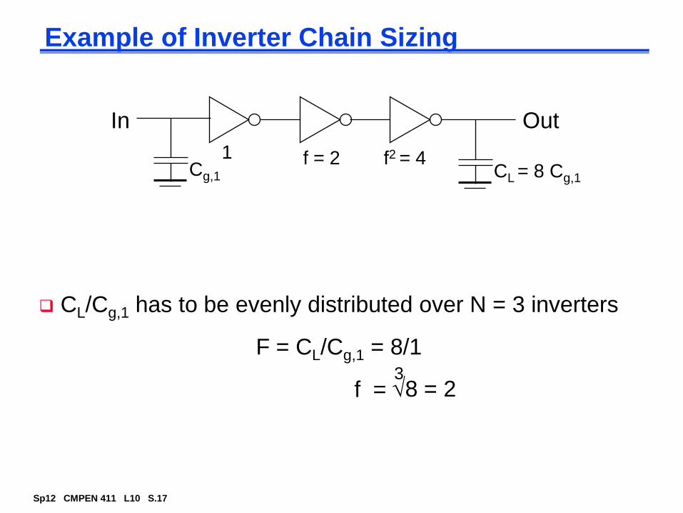
Example of Inverter Chain Sizing
CL/Cg,1 has to be evenly distributed over N = 3 inverters
F = CL/Cg,1 = 8/1
f =
In Out
CL = 8 Cg,1Cg,1
1 f = 2 f2 = 4
38 = 2
Sp12 CMPEN 411 L10 S.18
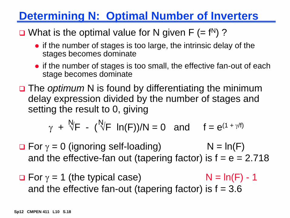
Determining N: Optimal Number of Inverters
What is the optimal value for N given F (= fN) ?
if the number of stages is too large, the intrinsic delay of the stages becomes dominate
if the number of stages is too small, the effective fan-out of each stage becomes dominate
N N
The optimum N is found by differentiating the minimum delay expression divided by the number of stages and setting the result to 0, giving
+ F - ( F ln(F))/N = 0 and f = e(1 + /f)
For = 0 (ignoring self-loading) N = ln(F)
and the effective-fan out (tapering factor) is f = e = 2.718
For = 1 (the typical case) N = ln(F) - 1
and the effective fan-out (tapering factor) is f = 3.6
Sp12 CMPEN 411 L10 S.19
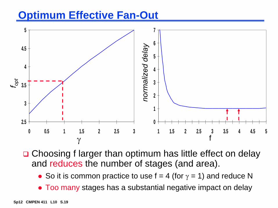
Optimum Effective Fan-Out
Choosing f larger than optimum has little effect on delay and reduces the number of stages (and area).
So it is common practice to use f = 4 (for = 1) and reduce N
Too many stages has a substantial negative impact on delay
2.5
3
3.5
4
4.5
5
0 0.5 1 1.5 2 2.5 3
0
1
2
3
4
5
6
7
1 1.5 2 2.5 3 3.5 4 4.5 5
f
Sp12 CMPEN 411 L10 S.20
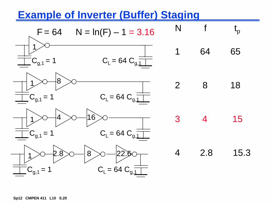
Example of Inverter (Buffer) Staging
CL = 64 Cg,1Cg,1 = 1
1
CL = 64 Cg,1Cg,1 = 1
1 8
CL = 64 Cg,1Cg,1 = 1
1 4 16
CL = 64 Cg,1Cg,1 = 1
1 2.8 8 22.6
N f tp
1 64 65
2 8 18
3 4 15
4 2.8 15.3
N = ln(F) – 1 = 3.16F = 64
Sp12 CMPEN 411 L10 S.21
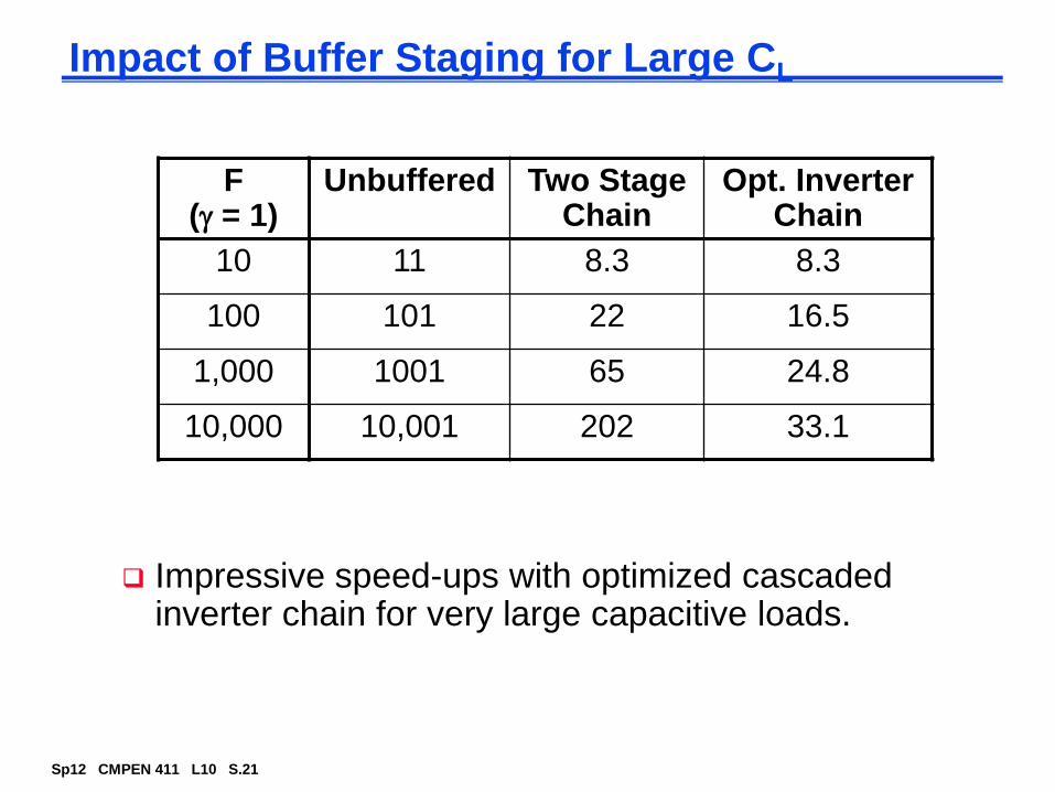
Impact of Buffer Staging for Large CL
Impressive speed-ups with optimized cascaded inverter chain for very large capacitive loads.
F ( = 1)
Unbuffered Two Stage Chain
Opt. Inverter Chain
10 11 8.3 8.3
100 101 22 16.5
1,000 1001 65 24.8
10,000 10,001 202 33.1
Sp12 CMPEN 411 L10 S.22
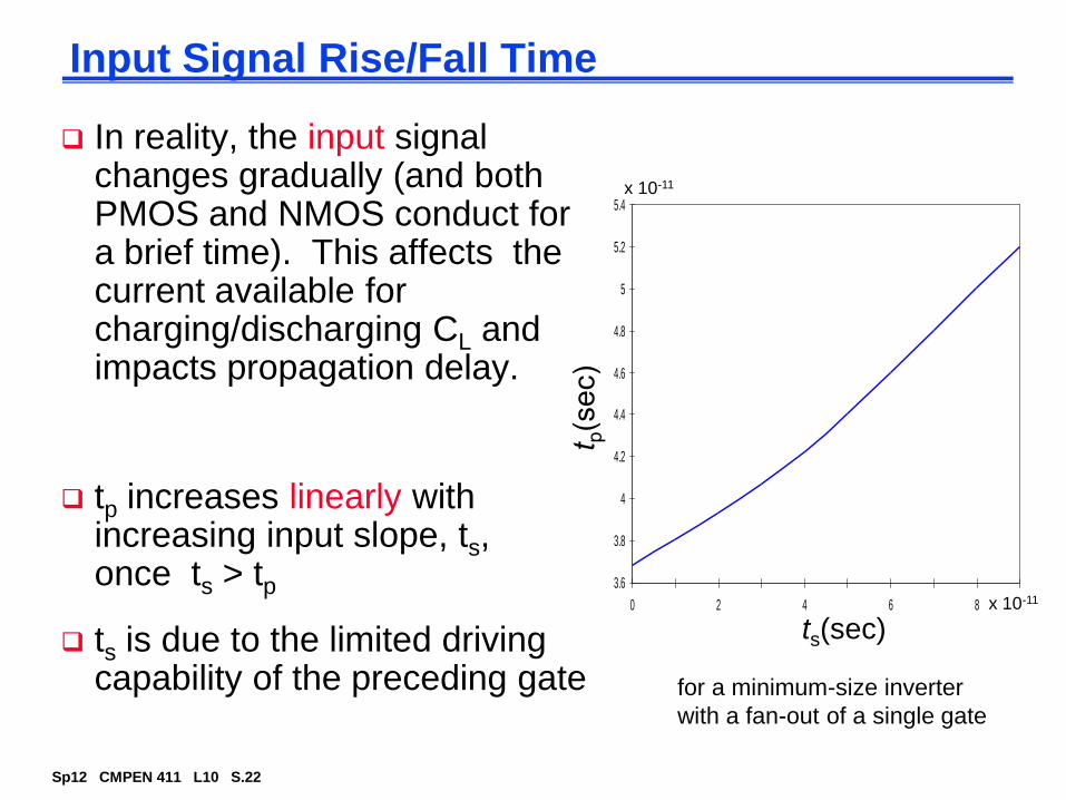
Input Signal Rise/Fall Time
In reality, the input signal changes gradually (and both PMOS and NMOS conduct for a brief time). This affects the current available for charging/discharging CL and impacts propagation delay.
3.6
3.8
4
4.2
4.4
4.6
4.8
5
5.2
5.4
0 2 4 6 8
ts(sec)
x 10-11
x 10-11
for a minimum-size inverter
with a fan-out of a single gate
tp increases linearly with increasing input slope, ts, once ts > tp
ts is due to the limited driving capability of the preceding gate
Sp12 CMPEN 411 L10 S.23
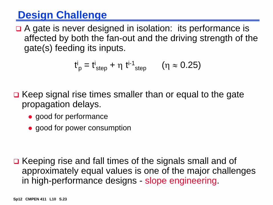
Design Challenge
A gate is never designed in isolation: its performance is affected by both the fan-out and the driving strength of the gate(s) feeding its inputs.
tip = tistep + ti-1step ( 0.25)
Keep signal rise times smaller than or equal to the gate propagation delays.
good for performance
good for power consumption
Keeping rise and fall times of the signals small and of approximately equal values is one of the major challenges in high-performance designs - slope engineering.
Sp12 CMPEN 411 L10 S.24
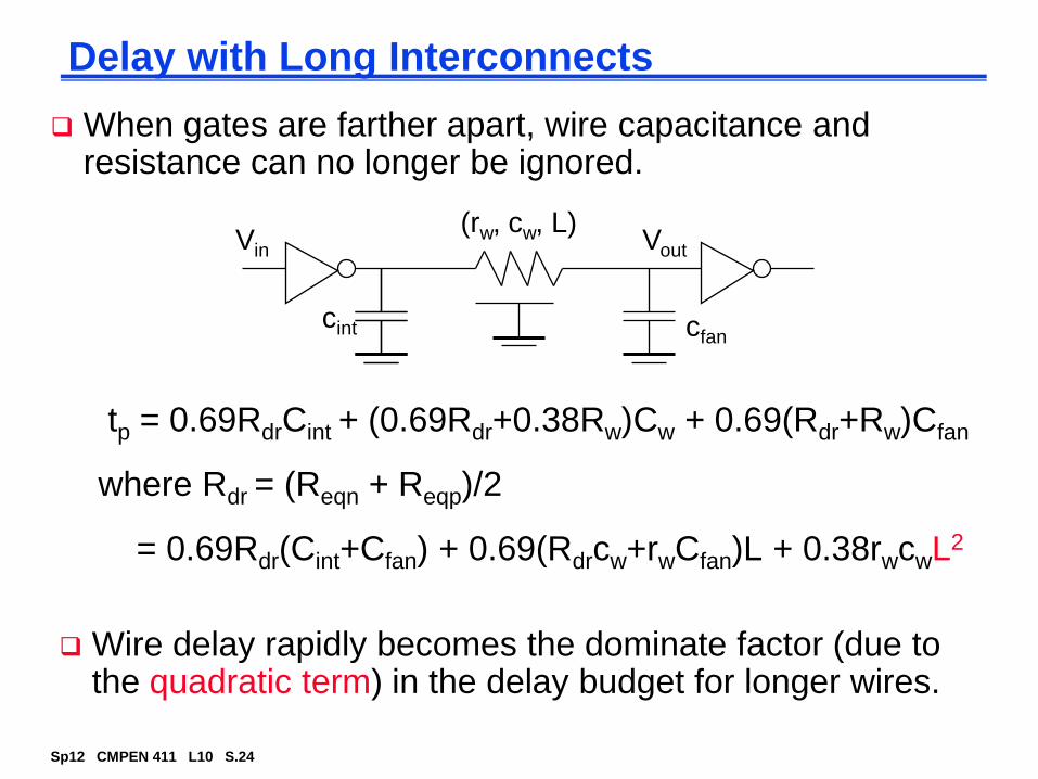
Delay with Long Interconnects
When gates are farther apart, wire capacitance and resistance can no longer be ignored.