Page 1
THE PENNSYLVANIA STATE UNIVERSITY
CMPEN411 Memory Chip Design Project Report
RAM64X6,SERIAL RAM 64X4 and DPRAM64X4
Qianqian Zhang
3/9/2012
MOSIS Chip Fabrication
Design Number: 85704
Fab-ID: V17L-CX
Acknowledgement:
I thank MOSIS and ON Semiconductor for their support which made the
fabrication of this class project possible.
Page 2
1
Table of Content
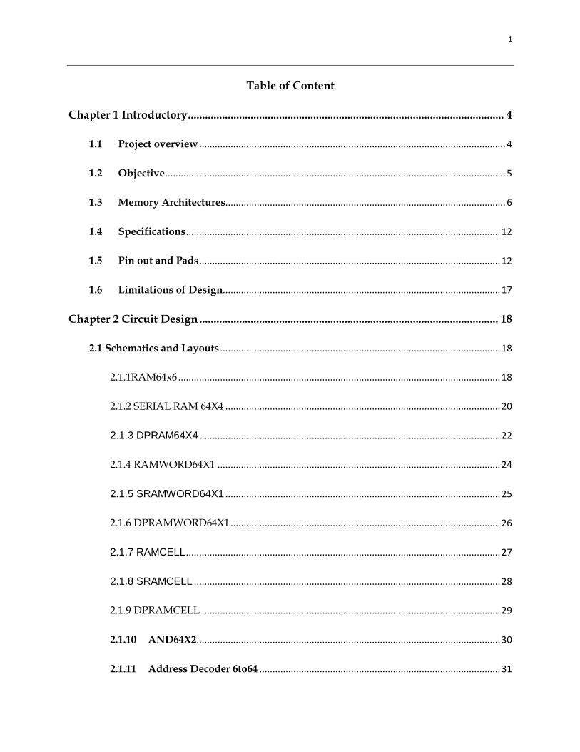
Chapter 1 Introductory ............................................................................................................... 4
1.1 Project overview ..................................................................................................................... 4
1.2 Objective .................................................................................................................................. 5
1.3 Memory Architectures........................................................................................................... 6
1.4 Specifications ........................................................................................................................ 12
1.5 Pin out and Pads ................................................................................................................... 12
1.6 Limitations of Design.......................................................................................................... 17
Chapter 2 Circuit Design ......................................................................................................... 18
2.1 Schematics and Layouts ........................................................................................................... 18
2.1.1RAM64x6 ........................................................................................................................... 18
2.1.2 SERIAL RAM 64X4 ......................................................................................................... 20
2.1.3 DPRAM64X4 ................................................................................................................... 22
2.1.4 RAMWORD64X1 ............................................................................................................ 24
2.1.5 SRAMWORD64X1 ......................................................................................................... 25
2.1.6 DPRAMWORD64X1 ....................................................................................................... 26
2.1.7 RAMCELL ........................................................................................................................ 27
2.1.8 SRAMCELL ..................................................................................................................... 28
2.1.9 DPRAMCELL .................................................................................................................. 29
2.1.10 AND64X2 .................................................................................................................... 30
2.1.11 Address Decoder 6to64 ............................................................................................ 31
Page 3
2
2.1.12 D Flip Flop ................................................................................................................. 32
2.1.13 And2 ............................................................................................................................ 34
2.1.14 And6 ................................................................................................................................ 35
2.1.15 Tristate buffer ............................................................................................................... 36
2.1.16 Inverter ........................................................................................................................... 37
Chapter 3 Circuit Performance ............................................................................................... 38
3.1 simulation result ......................................................................................................................... 38
3.1.1 RAM64X6 ......................................................................................................................... 38
3.1.2 SERIAL RAM 64X4 ......................................................................................................... 39
3.1.3 DPRAM64X4 .................................................................................................................... 40
3.2 Discussion of the simulation results ........................................................................................ 41
Chapter 4 Verification .............................................................................................................. 42
4.1 DRC and LVS Verification ........................................................................................................ 42
4.2 Simulation of Extracted View ................................................................................................... 43
4.2.1 RAM64X6 ........................................................................................................................... 43
4.2.2 Serial RAM 64X4 ................................................................................................................. 44
4.2.3 DPRAM64x4 ....................................................................................................................... 44
4.2.4 Input Pad .......................................................................................................................... 46
4.2.5 Inout Pad .......................................................................................................................... 47
Chapter 5 Experimental Results ............................................................................................. 48
Chapter 6 Summary and Conclusion .................................................................................... 50
Page 4
3
Appendix A ................................................................................................................................ 51
Appendix B ................................................................................................................................. 53
Appendix C ................................................................................................................................ 55
Appendix D ................................................................................................................................ 56
Page 5
4
Chapter 1 Introductory
1.1 Project overview
This is a memory chip design project with CMPEN 411 class and extended to independent
study with design, fabrication, and testing. This chip design has three memories: a RAM64X6, a
SERIAL RAM 64X4 and a Dual Port Ram 64x4 based on ami06 (λ=0.3) technology. The logic
structure had been tested in VHDL running on Xilinx ISE 12.2 first. Due to the three memory
designs contains too many I/Os and fabrication pin number is fixed to be 40, some signals need
to share the same pin. However, the three memory chip can still work individually.
Figure 1.1 Final Layout Design
Page 6
5
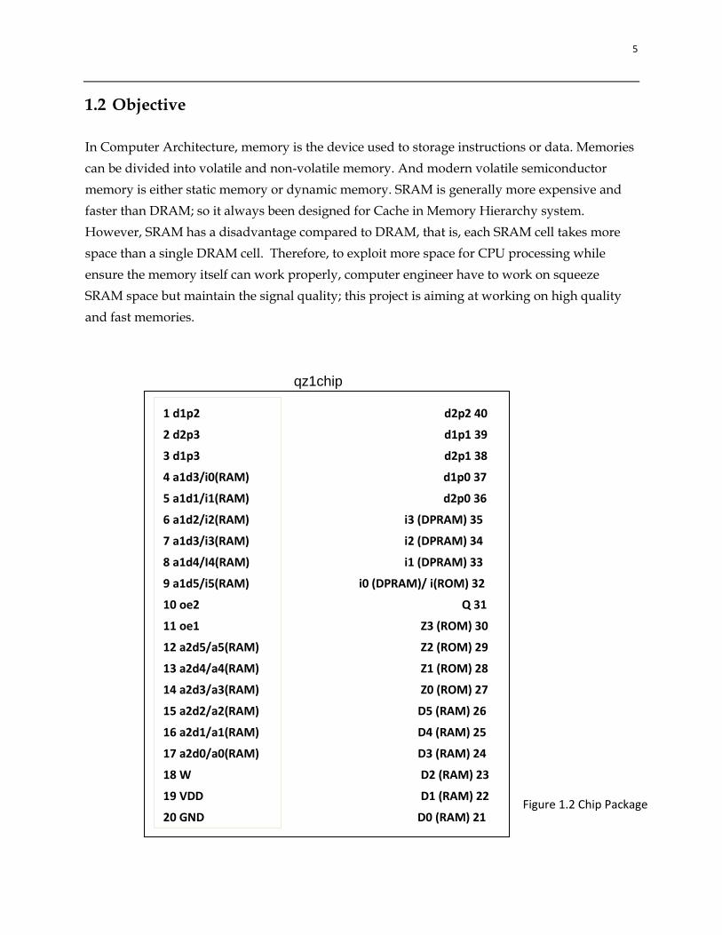
1.2 Objective
In Computer Architecture, memory is the device used to storage instructions or data. Memories
can be divided into volatile and non-volatile memory. And modern volatile semiconductor
memory is either static memory or dynamic memory. SRAM is generally more expensive and
faster than DRAM; so it always been designed for Cache in Memory Hierarchy system.
However, SRAM has a disadvantage compared to DRAM, that is, each SRAM cell takes more
space than a single DRAM cell. Therefore, to exploit more space for CPU processing while
ensure the memory itself can work properly, computer engineer have to work on squeeze
SRAM space but maintain the signal quality; this project is aiming at working on high quality
and fast memories.
qz1chip
1 d1p2
2 d2p3
3 d1p3
4 a1d3/i0(RAM)
5 a1d1/i1(RAM)
6 a1d2/i2(RAM)
7 a1d3/i3(RAM)
8 a1d4/I4(RAM)
9 a1d5/i5(RAM)
10 oe2
11 oe1
12 a2d5/a5(RAM)
13 a2d4/a4(RAM)
14 a2d3/a3(RAM)
15 a2d2/a2(RAM)
16 a2d1/a1(RAM)
17 a2d0/a0(RAM)
18 W
19 VDD
20 GND
d2p2 40
d1p1 39
d2p1 38
d1p0 37
d2p0 36
i3 (DPRAM) 35
i2 (DPRAM) 34
i1 (DPRAM) 33
i0 (DPRAM)/ i(ROM) 32
Q 31
Z3 (ROM) 30
Z2 (ROM) 29
Z1 (ROM) 28
Z0 (ROM) 27
D5 (RAM) 26
D4 (RAM) 25
D3 (RAM) 24
D2 (RAM) 23
D1 (RAM) 22
D0 (RAM) 21 Figure 1.2 Chip Package
Page 7
6
1.3 Memory Architectures
Figure 1.3 RAM64X6 Logic Block
This RAM has 6 bit inputs and outputs, 64 address location. Inputs are i0 – i5 and
outputs are d0 – d5. AND Gate 64x2 module contains 64 AND Gates; for all the 64
AND Gates, they share the same input B from W signal and different input A from
the outputs of address decoder 6 to 64, which is t0 – t63. And the ramword64x1’s
logic structure is presented below:
Page 8
7
Figure 1.4 ramword64x1 logic block
Each ramword64x1 has 64 ramcell. When the ramword been put together to form
the whole ram64x6, the input D0-D63 will be all connected to one bit of the input of
RAM; and the output Z0 – Z63 will also be connected to one bit of the output of
RAM. Besides, the CK signal will be controlled by the 6 to 64 address decoder and
the e0 – e63 signal will be all connected to OE signal.
Page 9
8
Figure 1.5 SERIAL RAM 64X4 logic block
SERIAL RAM 64X4 has only one input i and five outputs. Outputs are Z0 – Z3 and
Q; Output Q is the output of the 64th address location. So only after 64 shift terms, Q
will equal to i. Z0 continues shifting one bit after input i, Z1 shifts one bit after Z0,
Z2 shifts one bit after Z1 and Z3 shifts one bit after Z2. T0-63 will be connected to
the W signal in SRAMWORD64x1. Below is the logic block for Serial Ram 64x1:
Page 10
9
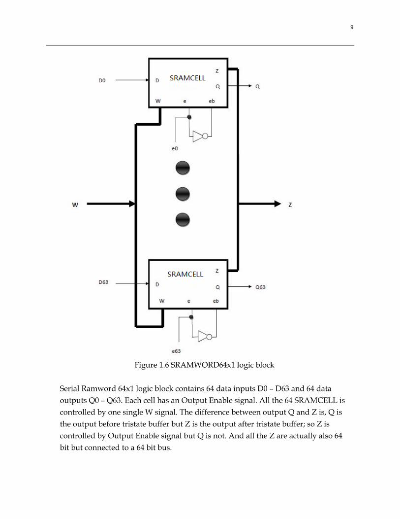
Figure 1.6 SRAMWORD64x1 logic block
Serial Ramword 64x1 logic block contains 64 data inputs D0 – D63 and 64 data
outputs Q0 – Q63. Each cell has an Output Enable signal. All the 64 SRAMCELL is
controlled by one single W signal. The difference between output Q and Z is, Q is
the output before tristate buffer but Z is the output after tristate buffer; so Z is
controlled by Output Enable signal but Q is not. And all the Z are actually also 64
bit but connected to a 64 bit bus.
Page 11
10
Figure 1.7 DPRAM64X4 logic block
This dual port ram has 4 bit inputs and outputs. There are three address decoders
and they are all 6 to 64; one is for write, two for read. For the write address decoder,
its input is a0-a5; two read address decoders are for the two ports. At Port 1, the
address inputs are a1d0 – a1d5; at Port 2, the address inputs are a2d0 – d2d5. And
the data output from Port 1 is d0p1 – d5p1; and the data output from Port 2 is d0p2
– d5p2. In addition, a dpramword64x1 logic block is presented below
Page 12
11
Figure 1.8 dpramword64x1 logic block
The module above has 64 dpramcells. All 64 dpramcells share the same D input, W
input does Write function when is it 1 and does read function when it is 0, two
different output enable signals individually control the two different output ports.
Page 13
12
1.4 Specifications
Table 1.1 Specification
Name Specification
VSS GND
VDD 2.5V – 6V
1.5 Pin out and Pads Pin Pad Type Name Description
1 Inout d1p2 D2 of Port1 (DPRAM)
2 Inout d2p3 D3 of Port2 (DPRAM)
3 Input d1p3 D3 of Port1 (DPRAM)
4 Input a1d0/i0(RAM) a3 of Port 1(DPRAM) and i0 (RAM)
5 input a1d1/i1(RAM) a1 of Port 1(DPRAM) and i1 (RAM)
6 Input a1d2/i2(RAM) a2 of Port 1 (DPRAM) and i2 (RAM)
7 Input a1d3/i3(RAM) a3 of Port 1 (DPRAM) and i3 (RAM)
8 input a1d4/i4(RAM) a4 of Port 1 (DPRAM) and i4 (RAM)
9 Input a1d5/i5(RAM) a5 of Port 1 (DPRAM) and i5 (RAM)
10 Input Oe2 Output enable of port 2 of DPRAM
11 input Oe1 Output enable of RAM and ROM/output enable of the Port 1 of DPRAM
12 Input a2d5/a5 a5 of Port 2(DPRAM) and a5(RAM and ROM)
13 Input a2d4/a4 a4 of Port 2(DPRAM) and a4(RAM and ROM)
14 input a2d3/a3 a3 of Port 2(DPRAM) and a3(RAM and ROM)
15 Input a2d2/a2 a2 of Port 2(DPRAM) and a2(RAM and ROM)
16 Input a2d1/a1 a1 of Port 2(DPRAM) and a1(RAM and ROM)
17 input a2d0/a0 a0 of Port 2(DPRAM) and a0(RAM and ROM)
18 Input W W signal of DPRAM, RAM and ROM
19 VDD VDD VDD
20 GND GND GND
21 Inout D0(RAM) Data output of RAM
22 Inout D1(RAM) Data output of RAM
23 Inout D2(RAM) Data output of RAM
24 inout D3(RAM) Data output of RAM
25 Inout D4(RAM) Data output of RAM
26 Inout D5(RAM) Data output of RAM
27 Inout Z0(ROM) D0 of ROM
28 inout Z1(ROM) D1 of ROM
29 Inout Z2(ROM) D2 of ROM
30 Inout Z3(ROM) D3 of ROM
31 Inout Q Output of ROM
Page 14
13
32 Input i0(DPRAM) Input of DPRAM
33 Input i1(DPRAM) Input of DPRAM
34 Input i2(DPRAM) Input of DPRAM
35 Input i3(DPRAM) Input of DPRAM
36 inout d2p0 D0 of Port 2 (DPRAM)
37 Input d1p0 D0 of Port 1 (DPRAM)
38 Input d2p1 D1 of Port 2 (DPRAM)
39 Input d1p1 D1 of Port 1 (DPRAM)
40 input d2p2 D2 of Port 2 (DPRAM)
Page 15
14
Pin 15
Pin14 Pin 13
Pin 12
Pin 11
Pin 10
Pin 9 Pin 8 8
Pin 7
Pin 6
a2d2 a2 a2
a2d3 a3 a3
a2d4 a4 a4
a2d5 a5 a5
oe1 oe oe
oe2 a1d5 i5
a1d4 i4
a1d3 i3
a1d2 i2
Pin 16
a2d1 a1 a1
input input input input input input input input input
Input a1d1 i1)
Pin 5
Pin 17
a2d0 a0 a0
input Input a1d0 i0
Pin 4
Pin 18
W W W
Input Inout d1p3 Pin 3
Pin 19
VDD Input Inout d2p3 Pin 2
Pin 20
GND Input RAM 64X6
ROM 64X4
DPRAM 64X4
Inout d1p2 Pin 1
Pin 21
D0
Inout Inout d2p2 Pin 40
Pin 22
D1
Inout Inout d1p1 Pin 39
Pin 23
D2
Inout Inout d2p1 Pin 38
Pin 24
D3
Inout Inout d1p0 Pin 37
Pin 25
D4
Inout inout inout inout inout inout input input input
Inout input
d2p0 Pin 36
D5
Z0
Z1
Z2
Z3
Q i0 i
i1
i2
i3
Pin 26
Pin 27
Pin 28
Pin 29
Pin 30
Pin 31
Pin 32
Pin 33
Pin 34
Pin 35
Figure 1.9 overall pin layout
Page 16
15
Figure 1.10 Pad_Input
Figure 1.11 Pad_Inout
Page 17
16
Figure 1.12 Pin_VDD
Figure 1.13 Pin_gnd
Page 18
17
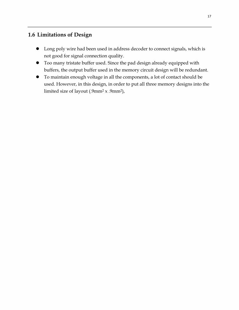
1.6 Limitations of Design
Long poly wire had been used in address decoder to connect signals, which is
not good for signal connection quality.
Too many tristate buffer used. Since the pad design already equipped with
buffers, the output buffer used in the memory circuit design will be redundant.
To maintain enough voltage in all the components, a lot of contact should be
used. However, in this design, in order to put all three memory designs into the
limited size of layout (.9mm2 x .9mm2),
Page 19
18
Chapter 2 Circuit Design
2.1 Schematics and Layouts
2.1.1RAM64x6
Figure 2.1.1 RAM64X6 schematic
The schematic above presents 8 symbols represents for address decoder 6 to 64, And
Gate 64x2 and 6 ramword64x1 separately. And they are connected with 64 bit buses.
Ramword64x1
And64x2 Address
Decoder
6 to 64
Page 20
19
The output of each ramword64x1 is connected to a inverter buffer and those buffers are
controlled by a common output enable signal.
Figure 2.1.2 RAM64X6 Layout
On the module above, there are 8 long columns combined together. From the left to the
right, address decoder 6 to 64, and gate 64x2, and 6 ramword64x1. Also, there are 6
inverter buffers on the top of ramword64x1 which connect to the output.
Page 21
20
2.1.2 SERIAL RAM 64X4
Figure 2.2.1 SERIAL RAM 64X4 Schematic
On the schematic, four big square symbols are representing SRAMWORD64x1 and
one big rectangular symbol on the left bottom side is representing address decoder 6
to 64. The buses connecting them are 64 bit. The outputs from each
SRAMWORD64x1 all goes to an inverter buffer which controlled by a common
output enable signal.
SRAMWORD64
x1
Address
Decoder
6 to 64
Page 22
21
Figure 2.2.2 Serial RAM 64X4 Layout
This module consists of 5 long columns. From left to right, address decoder 6 to 64 and
4 romword64x1. On the top of 4 romword64x1, there are four tristate buffers.
Page 23
22
2.1.3 DPRAM64X4
Figure 2.3.1 DPRAM64X4 schematic
On the schematic showed above, the four square symbols in the middle represents
four dpramword64x1. Three rectangular symbols represent address decoder 6 to 64.
The square symbol on the top is AND Gate 64x2. The difference between dpram and
ram is dpram has two output ports. Port 1 and Port 2 both have 4 bit outputs; and
they all goes to tristate buffers controlled by a common output enable signal.
Write address
Decoder 6 to 64
Port1 Read
address
Decoder
6 to 64
Port2 Read
address
Decoder
6 to 64
Dpramword64x1
AND Gate
64x2
Page 24
23
Figure 2.3.2 DPRAM64X4 Layout
This module consists of 8 long columns. From the left to right, read port 1 address decoder 6 to
64, address decoder 6 to 64 write port, and gate 64x2, 4 dual port ramwords, and read port 2
address decoder 6 to 64.
Page 25
24
2.1.4 RAMWORD64X1
Figure 2.4.1 ramword64x1 schematic
Figure 2.4.2 ramword64x1 layout
This module consists of 64 ramcells which form a column. Both the schematics and
layout pictures well present how the 64 ramcells are connected by buses.
Page 26
25
2.1.5 SRAMWORD64X1
Figure 2.5.2 SRAMWORD64x1 schematic Figure 2.5.1 serial ram 64x1 layout
Page 27
26
2.1.6 DPRAMWORD64X1
Figure 2.6.1 dpramword64x1 schematic
Figure 2.6.2 dpramword64x1 layout
Page 28
27
2.1.7 RAMCELL
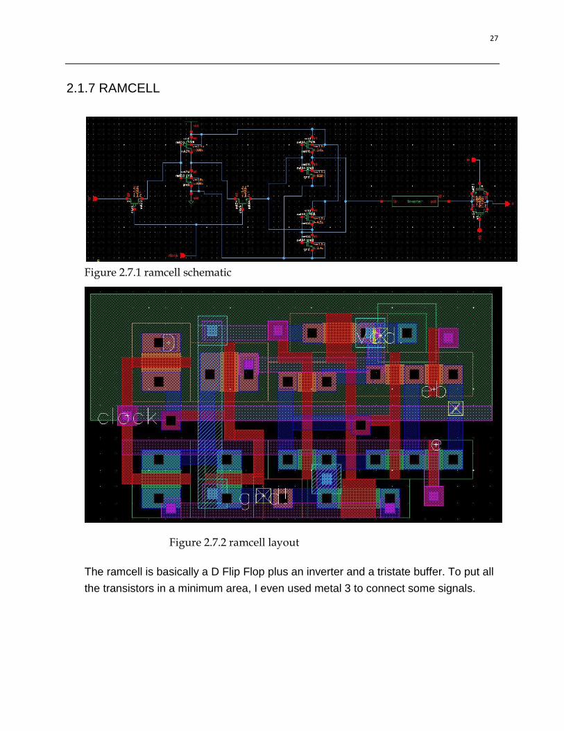
Figure 2.7.1 ramcell schematic
The ramcell is basically a D Flip Flop plus an inverter and a tristate buffer. To put all
the transistors in a minimum area, I even used metal 3 to connect some signals.
Figure 2.7.2 ramcell layout
Page 29
28
2.1.8 SRAMCELL
Figure 2.8.1 SRAMCELL schematic
Figure 2.8.2 Serial RAM cell layout
Page 30
29
2.1.9 DPRAMCELL
Figure 2.9.1 dpramcell schematic
Figure 2.9.2 Dual Port RAM cell Layout
Dual Port Ram cell is obviously larger than ramcell and serial ram cell because it
has two output ports. Even though I used metal 1, metal 2 and metal 3 to connect
this single cell, I only use metal 3 to connect signals vertically and metal 2 to
connect signals horizontally.
Page 31
30
2.1.10 AND64X2
Figure 2.10.1 And Gate 64x2 schematic Figure 2.10.2 AND Gate 64x2 layout
This module is different from the other 64 bit module that I built before; the 64 AND
Gates in the column does not connected to each other, they are individually working
component.
Page 32
31
2.1.11 Address Decoder 6to64
Figure 2.11.1 6 to 64 address decoder schematic
Figure 2.11.2 address decoder 6 to 64 layout
This module consists 64 AND Gates and 6 inverters on the top for the inputs. 6 inveters
works as decoder to specify 64 address location.
Page 33
32
2.1.12 D Flip Flop
Figure 2.12.1 D Flip Flop Schematic
Page 34
33
Figure 2.12.2 D Flip Flop Layout
Page 35
34
2.1.13 And2
Figure 2.13.1 AND2 Gate schematic
Figure 2.13.2 AND 2 Gate layout
Page 36
35
2.1.14 And6
Figure 2.14.1 AND6 Gate schematic
Figure 2.14.2 AND 6 Gate layout
To reduce delay due to fan-in, I used two 3 input AND Gate, and connect them to a 2
input AND Gate.
Page 37
36
2.1.15 Tristate buffer
Figure 2.15.1 inverter buffer schematic
Figure 2.14.2 Tristate Buffer
Layout
Page 38
37
2.1.16 Inverter
Figure 2.16.1 inverter schematic Figure 2.16.2 Inverter
layout From the schematic to layout, even though this is a simple component, I tried my best to put the two transistors within the minimum area. In the layout, the distance between PMOS and NMON is the minimum distance required. Also, for all the connecting wires used such as poly and metal 1, they are all built with minimum width. Because this component will be used very often in larger component, it naturally has a larger demand in smaller size design.
Page 39
38
Chapter 3 Circuit Performance
3.1 simulation result
3.1.1 RAM64X6
Figure 3.1 RAM64X4 Schematic Simulation
In the simulation above, the first four clock cycles are writing cycles and the last four
clock cycles are reading cycles. I wrote data #101010, #010101, #000000 and #111111
into address location 0, 1, 2 and 3 sequentially; and then reading from address location 0,
1, 2 and 3, result datum are #101010, #010101, #000000 and #111111 which confirmed
what I stored into the memory.
Page 40
39
3.1.2 SERIAL RAM 64X4
Figure 3.2 Serial RAM 64x4 Schematic Simulation
This Serial RAM 64x4 has an input i, and Z0 outputs shift one bit after it; Z1 shifts one
bit after Z0, Z2 shifts one bit after Z1; Z3 shifts one bit after Z2. Q is supposed to output
I after 64 cycles but did not show on the simulation result due to timing is not long
enough.
Page 41
40
3.1.3 DPRAM64X4
Figure 3.3 DPRAM64x4 schematic simulation
In the first four cycles are writing cycles, the last four cycles are reading cycles. During
the writing cycles, I wrote #1011, #0100, #1001 and #0010 into address location 000000,
010101, 101010 and 111111 sequentially. Then I read data from memory address location
000000, 010101, 101010 and 111111 from both ports at the same time. The resulting data
are corresponded to those that I input.
Page 42
41
3.2 Discussion of the simulation results
On the simulation result of RAM64X4 schematic, the worst delay is 10ns at the reading
cycle. For Serial RAM 64x4, the worst delay is 2.5 ns. And the DPRAM 64X4 has a worst
delay of 12ns.
Page 43
42
Chapter 4 Verification
4.1 DRC and LVS Verification
All the components of the three memory chip design had passed DRC checking and the
netlists and schematics matched in the LVS Verification. No error found. The net list
generated by LVS Verification of all three memory designs are listed in Appendix D.
Page 44
43
4.2 Simulation of Extracted View
4.2.1 RAM64X6
Figure 4.1 RAM64X6 extracted file simulation
Page 45
44
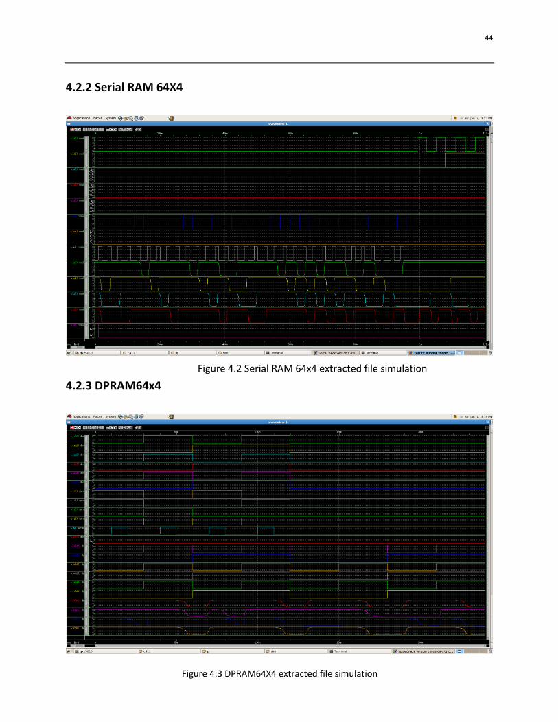
4.2.2 Serial RAM 64X4
4.2.3 DPRAM64x4
Figure 4.2 Serial RAM 64x4 extracted file simulation
Figure 4.3 DPRAM64X4 extracted file simulation
Page 47
46
4.2.4 Input Pad
Figure 4.4 Input Pad layout extracted file simulation
Page 48
47
4.2.5 Inout Pad
Figure 4.5 Inout Pad extracted file simulation
Page 49
48
Chapter 5 Experimental Results
I used PIC18F4550 microprocessor to send out input lines and wrote PicBasic Code to
run the test circuit. The microprocessor is a EEPROM and the code was written in PICit
2 software and programmed to the chip from a USB port connected to my laptop. The
test circuit layout (See Appendix C) was designed on Multisim and Ultiboard.
Figure 5.1 Rising edge
On the oscilloscope screen shot, each grid is 10ns. So the delay of the rising edge is
approximately 15ns.
Page 50
49
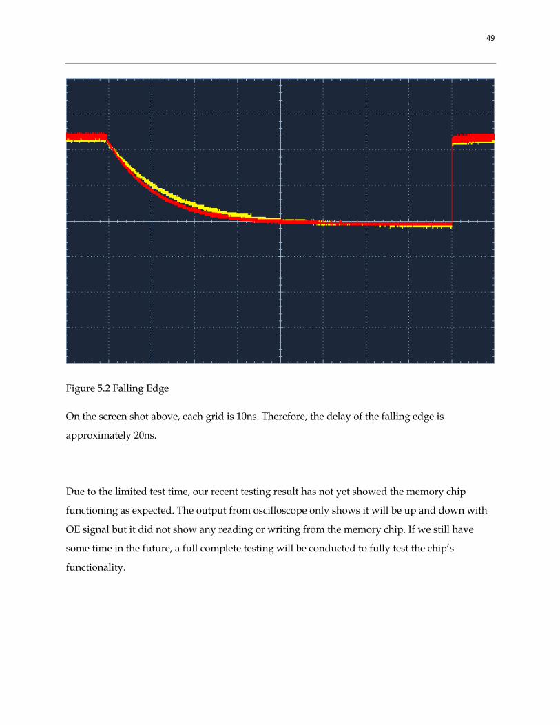
Figure 5.2 Falling Edge
On the screen shot above, each grid is 10ns. Therefore, the delay of the falling edge is
approximately 20ns.
Due to the limited test time, our recent testing result has not yet showed the memory chip
functioning as expected. The output from oscilloscope only shows it will be up and down with
OE signal but it did not show any reading or writing from the memory chip. If we still have
some time in the future, a full complete testing will be conducted to fully test the chip’s
functionality.
Page 51
50
Chapter 6 Summary and Conclusion
This is a large project and it still worth to optimize. The delay measured from the real
experiment test is greater the simulation test. I think one of the advantages of this
memory design is the D Flip Flop design. A good D Flip Flop design will squeeze the
whole memory area and maintain the good quality signal processing. Also, 64-cell
column model design plays an important role in each memory’s floor plan.
The designing cost for this project is almost free because I did work on Solaris Machine
provided by CSE department of Pennsylvania State University. A test circuit board cost
$25 ordered on PCBnet.com; the PIC18F4550 chip and chip programming board is from
the tool that I used in my Embedded Systems Course. A power consumption analysis
of each memory is listed below:
Memory Aear(um2) T(ns) Power dissipation(um2•ns2)
RAM64x6 213.85x873.45 10 1860448.5
Serial RAM 64x4 151.85x860.7 2.5 326743.2375
DPRAM 64x4 280.05x878.7 12 2952959.22
However, due to long poly wire used and redundant tristate buffers used in the circuit
design, this project still have obvious defects. If I had one more chance to redesign this
chip, I will test the inner circuit with pad together and see the real delay in simulation.
Furthermore, there is still a lot to think about improvement in the memory floor plan.
Because memory is a basic device in processor, the inputs and outputs need to be
connected to the controls of the processor; a vertical rectangular shape of memory
might not be a good shape to adjust to the other component of processors. Next time, I
will try to design the memory in square shape (approximately) which can be laid in the
middle of a processor and easily have inputs and outputs connected to other controls.
Page 52
51
Appendix A
Figure A.1 real chip side
Figure A.2 real chip top face
Page 53
52
Figure A.3 real chip top2
Page 54
53
Appendix B
Figure B.3.2x
Page 56
55
Appendix C
Figure C.1 test PCB layout view
Page 57
56
Appendix D
RAM64X6
@(#)$CDS: LVS version 6.1.4-64b 03/30/2011 00:45 (sjfdl230) $
Command line: /home/software/cadence-2009/IC610/tools.lnx86/dfII/bin/64bit/LVS -dir
/home/noncse/qxz5010/c411/pj/LVS -l -s -t /home/noncse/qxz5010/c411/pj/LVS/layout
/home/noncse/qxz5010/c411/pj/LVS/schematic
Like matching is enabled.
Net swapping is enabled.
Using terminal names as correspondence points.
Compiling Diva LVS rules...
Net-list summary for /home/noncse/qxz5010/c411/pj/LVS/layout/netlist
count
3246 nets
22 terminals
3608 pmos
3608 nmos
Net-list summary for /home/noncse/qxz5010/c411/pj/LVS/schematic/netlist
count
3246 nets
22 terminals
3608 pmos
3608 nmos
Terminal correspondence points
N3231 N140 W
N3237 N150 a0
N3236 N141 a1
N3235 N151 a2
Page 58
57
N3234 N143 a3
N3233 N155 a4
N3232 N139 a5
N3229 N100 d0
N3228 N138 d1
N3227 N88 d2
N3226 N152 d3
N3225 N137 d4
N3224 N146 d5
N3230 N0 gnd!
N3244 N153 i0
N3243 N131 i1
N3242 N147 i2
N3241 N144 i3
N3240 N148 i4
N3239 N93 i5
N3245 N133 oeb
N3238 N1 vdd!
Devices in the netlist but not in the rules:
pcapacitor
Devices in the rules but not in the netlist:
cap nfet pfet nmos4 pmos4
The net-lists match.
layout schematic
instances
un-matched 0 0
rewired 0 0
size errors 0 0
pruned 0 0
active 7216 7216
total 7216 7216
Page 59
58
nets
un-matched 0 0
merged 0 0
pruned 0 0
active 3246 3246
total 3246 3246
terminals
un-matched 0 0
matched but
different type 0 0
total 22 22
Probe files from /home/noncse/qxz5010/c411/pj/LVS/schematic
devbad.out:
netbad.out:
mergenet.out:
termbad.out:
prunenet.out:
prunedev.out:
audit.out:
Probe files from /home/noncse/qxz5010/c411/pj/LVS/layout
devbad.out:
Page 60
59
netbad.out:
mergenet.out:
termbad.out:
prunenet.out:
prunedev.out:
audit.out:
Serial RAM 64x4
@(#)$CDS: LVS version 6.1.4-64b 03/30/2011 00:45 (sjfdl230) $
Command line: /home/software/cadence-2009/IC610/tools.lnx86/dfII/bin/64bit/LVS -dir
/home/noncse/qxz5010/c411/pj/LVS -l -s -t /home/noncse/qxz5010/c411/pj/LVS/layout
/home/noncse/qxz5010/c411/pj/LVS/schematic
Like matching is enabled.
Net swapping is enabled.
Using terminal names as correspondence points.
Compiling Diva LVS rules...
Net-list summary for /home/noncse/qxz5010/c411/pj/LVS/layout/netlist
count
2273 nets
16 terminals
2514 pmos
2514 nmos
Net-list summary for /home/noncse/qxz5010/c411/pj/LVS/schematic/netlist
count
Page 61
60
2273 nets
16 terminals
2514 pmos
2514 nmos
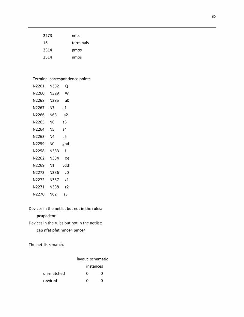
Terminal correspondence points
N2261 N332 Q
N2260 N329 W
N2268 N335 a0
N2267 N7 a1
N2266 N63 a2
N2265 N6 a3
N2264 N5 a4
N2263 N4 a5
N2259 N0 gnd!
N2258 N333 i
N2262 N334 oe
N2269 N1 vdd!
N2273 N336 z0
N2272 N337 z1
N2271 N338 z2
N2270 N62 z3
Devices in the netlist but not in the rules:
pcapacitor
Devices in the rules but not in the netlist:
cap nfet pfet nmos4 pmos4
The net-lists match.
layout schematic
instances
un-matched 0 0
rewired 0 0
Page 62
61
size errors 0 0
pruned 0 0
active 5028 5028
total 5028 5028
nets
un-matched 0 0
merged 0 0
pruned 0 0
active 2273 2273
total 2273 2273
terminals
un-matched 0 0
matched but
different type 0 0
total 16 16
Probe files from /home/noncse/qxz5010/c411/pj/LVS/schematic
devbad.out:
netbad.out:
mergenet.out:
termbad.out:
prunenet.out:
prunedev.out:
audit.out:
Page 63
62
Probe files from /home/noncse/qxz5010/c411/pj/LVS/layout
devbad.out:
netbad.out:
mergenet.out:
termbad.out:
prunenet.out:
prunedev.out:
audit.out:
DPRAM 64X4
@(#)$CDS: LVS version 6.1.4-64b 03/30/2011 00:45 (sjfdl230) $
Command line: /home/software/cadence-2009/IC610/tools.lnx86/dfII/bin/64bit/LVS -dir
/home/noncse/qxz5010/c411/pj/LVS -l -s -t /home/noncse/qxz5010/c411/pj/LVS/layout
/home/noncse/qxz5010/c411/pj/LVS/schematic
Like matching is enabled.
Net swapping is enabled.
Using terminal names as correspondence points.
Compiling Diva LVS rules...
Net-list summary for /home/noncse/qxz5010/c411/pj/LVS/layout/netlist
count
4173 nets
35 terminals
4650 pmos
Page 64
63
4650 nmos
Net-list summary for /home/noncse/qxz5010/c411/pj/LVS/schematic/netlist
count
4173 nets
35 terminals
4650 pmos
4650 nmos
Terminal correspondence points
N4169 N20 a1d0
N4168 N30 a1d1
N4167 N194 a1d2
N4166 N195 a1d3
N4165 N102 a1d4
N4164 N76 a1d5
N4148 N124 a2d0
N4147 N182 a2d1
N4146 N183 a2d2
N4145 N184 a2d3
N4144 N185 a2d4
N4143 N31 a2d5
N4154 N297 ai0
N4153 N35 ai1
N4152 N298 ai2
N4151 N37 ai3
N4150 N151 ai4
N4149 N29 ai5
N4161 N34 d0p1
N4160 N32 d0p2
N4140 N19 d1p1
N4139 N190 d1p2
N4163 N122 d2p1
N4162 N191 d2p2
Page 65
64
N4142 N36 d3p1
N4141 N192 d3p2
N4138 N0 gnd!
N4159 N189 i0
N4158 N33 i1
N4157 N186 i2
N4156 N187 i3
N4171 N188 oe1
N4170 N296 oe2
N4155 N1 vdd!
N4172 N28 w
Devices in the netlist but not in the rules:
pcapacitor
Devices in the rules but not in the netlist:
cap nfet pfet nmos4 pmos4
The net-lists match.
layout schematic
instances
un-matched 0 0
rewired 0 0
size errors 0 0
pruned 0 0
active 9300 9300
total 9300 9300
nets
un-matched 0 0
merged 0 0
pruned 0 0
active 4173 4173
total 4173 4173
Page 66
65
terminals
un-matched 0 0
matched but
different type 0 0
total 35 35
Probe files from /home/noncse/qxz5010/c411/pj/LVS/schematic
devbad.out:
netbad.out:
mergenet.out:
termbad.out:
prunenet.out:
prunedev.out:
audit.out:
Probe files from /home/noncse/qxz5010/c411/pj/LVS/layout
devbad.out:
netbad.out:
mergenet.out:
termbad.out:
prunenet.out:
Page 67
66
prunedev.out:
audit.out: