0 CARBON NANOTUBE ELECTRONICS: MODELING, PHYSICS, AND APPLICATIONS A Thesis Submitted to the Faculty ofPurdue University by Jing Guo In Partial Fulfillment of the Requirements for the Degree ofDoctor of Philosophy August, 2004
2.5 Electrostatic effect of the Contact geometry....................................................... 19
2.6 The band profile of a coaxially gated CNTFET with bulk electrodes and a
large gate underlap.............................................................................................. 22
2.7 The equilibrium conduction band edge for a coaxially gated CNTFET withthe gate oxide thickness tox=2nm, 8nm and 20nm ............................................. 23
2.8 The equilibrium conduction band edge at V G=0 for the CNTFET with
different source/drain contact radius, RC =0.7nm, 8nm, and 20nm....................24
3.1 An illustration of how continuum, ab initio, atomistic and semi-empirical
atomistic models will be combined in a multi-scale description of a carbon
3.2 The generic transistor with a molecule or device channel connected to the
source and drain contacts.................................................................................... 28
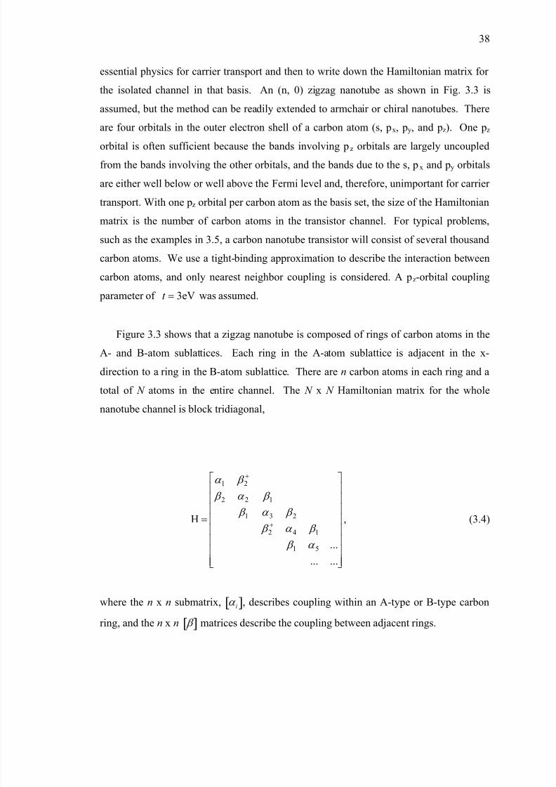
3.3 The schematic diagram of a (n, 0) zigzag nanotube ........................................... 32
3.4 The real space 2D lattice and the uncoupled, 1D mode space lattices of the(n,0) zigzag nanotube ......................................................................................... 37
3.8 The local-density-of-states (LDOS) and the electron density spectrum
computed by the real space approach ................................................................. 45
3.9 The I-V characteristics computed by the real space approach (the solid line)
and the mode space approach with 2 subbands (the circles) .............................. 473.10 The conduction band profile and charge density computed by the real
space approach (the solid lines) and the mode space approach.......................... 48
3.11 The coaxially gated Schottky barrier carbon nanotube transistor and its
Modeling, Physics, and Applications. Major Professor: Mark Lundstrom.
In recent years, significant progress in understanding the physics of carbon nanotube
electronic devices and in identifying potential applications has occurred. In a nanotube,
low bias transport can be nearly ballistic across distances of several hundred nanometers.
Deposition of high-κ gate insulators does not degrade the carrier mobility. The
conduction and valence bands are symmetric, which is advantageous for complementary
applications. The bandstructure is direct, which enables optical emission. Because of these attractive features, carbon nanotubes are receiving much attention. In this work,
simulation approaches are developed and applied to understand carbon nanotube device
physics, and to explore device engineering issues for better transistor performance.
Carbon nanotube field-effect transistors (CNTFETs) provide a concrete context for
exploring device physics and developing a simulation capability. We have developed an
empirical (pz orbital) atomistic, quantum simulator for nanotube transistors. Thissimulator uses the non-equilibrium Green’s function (NEGF) formalism to treat ballistic
transport in the presence of self-consistent electrostatics. We also separately developed a
coupled Monte-Carlo/quantum injection simulator to understand carrier scattering in
CNTFETs.
Numerical simulations are used to understand device physics and to explore device
engineering issues. In chapter 4, we did a comprehensive study of the scaling behaviorsfor ballistic SB CNTFETs. In chapter 5, we analyzed a short-channel, high-performance
CNTFET, to understand what controls and how to further improve the transistor
performance. In chapter 6, we explored the interesting role of phonon scattering in
Since the discovery of carbon nanotubes (CNTs) by Iijima in 1991[1], significant
progress has been achieved for both understanding the fundamental properties and
exploring possible engineering applications [2]. The possible application for
nanoelectronic devices has been extensively explored since the demonstration of the first
carbon nanotube transistors (CNTFETs) [3, 4]. Carbon nanotubes are attractive for
nanoelectronic applications due to its excellent electric properties. In a nanotube, low bias
transport can be nearly ballistic across distances of several hundred nanometers.
Deposition of high-κ gate insulators does not degrade the carrier mobility because the
topological structure results in an absence of dangling bonds. Fermi level pining at the
metal-nanotube interface is weak, so a range of Schottky barrier heights can be achieved
by using different contact metals. The conduction and valence bands are symmetric,
which is advantageous for complementary applications. The bandstructure is direct,
which enables optical emission, and finally, CNTs are highly resistant to electromigration.
Significant efforts have devoted to understand how a carbon nanotube transistor operates
and to improve the transistor performance [5, 6]. It has been demonstrated that most
CNTFETs to date operates like non-conventional Schottky barrier transistors [7, 8],
which results in quite different device and scaling behaviors from the MOSFET-like
transistors [9, 10]. Important techniques for significantly improving the transistor
performance, including the aggressively scaling of the nanotube channel, integration of
thin high-κ gate dielectric insulator [11, 12], use of excellent source/drain metal contacts[13], and demonstration of the self-align techniques, have been successfully developed.
Very recently, a nanotube transistor, which integrates ultra-short channel, thin high-κ top
gate insulator, excellent Pd source/drain contacts is demonstrated using a self-align
technique [14]. Promising transistor performance exceeding the state-of-the-art Si
MOSFETs is achieved. The transistor has a near-ballistic source-drain conductance of
he /45.0~ 2× and delivers a current of Aµ 20~ at |VG-VT|~1V.
In this work, numerical simulations are developed to explain experiments, tounderstand how the transistor operates and what controls the performance, and to explore
the approaches to improve the transistor performance. New simulation approaches are
necessary for a carbon nanotube transistor because it operates quite different from Si
transistors. The carbon nanotube channel is a quasi-one-dimensional conductor, which
has fundamentally different carrier transport properties from the Si MOSFET channel. It
has been demonstrated that treating the Schottky barriers at the metal/CNT interface and
near-ballistic transport in the channel are important for correctly modeling the transistor.
The CNT channel is a cylindrical semiconductor with a ~1nm diameter, which means the
electrostatic behavior of the transistor is quite different from Si MOSFETs with a 2D
electron gas. All carbon bonds are well satisfied at the carbon nanotube surface, which
results in a different semiconductor/oxide interface. Furthermore, the phonon vibration
modes and carrier scattering mechanisms are quite different in carbon nanotubes, which
results in different roles of phonon scattering in CNTFETs. In this work, we developed
physical simulation approaches to treat CNTFETs. We will show that our understanding
of the carrier transport, electrostatics, and interracial properties seem to be sufficient todescribe the behavior of the recently demonstrated short-channel CNTFETs [14].
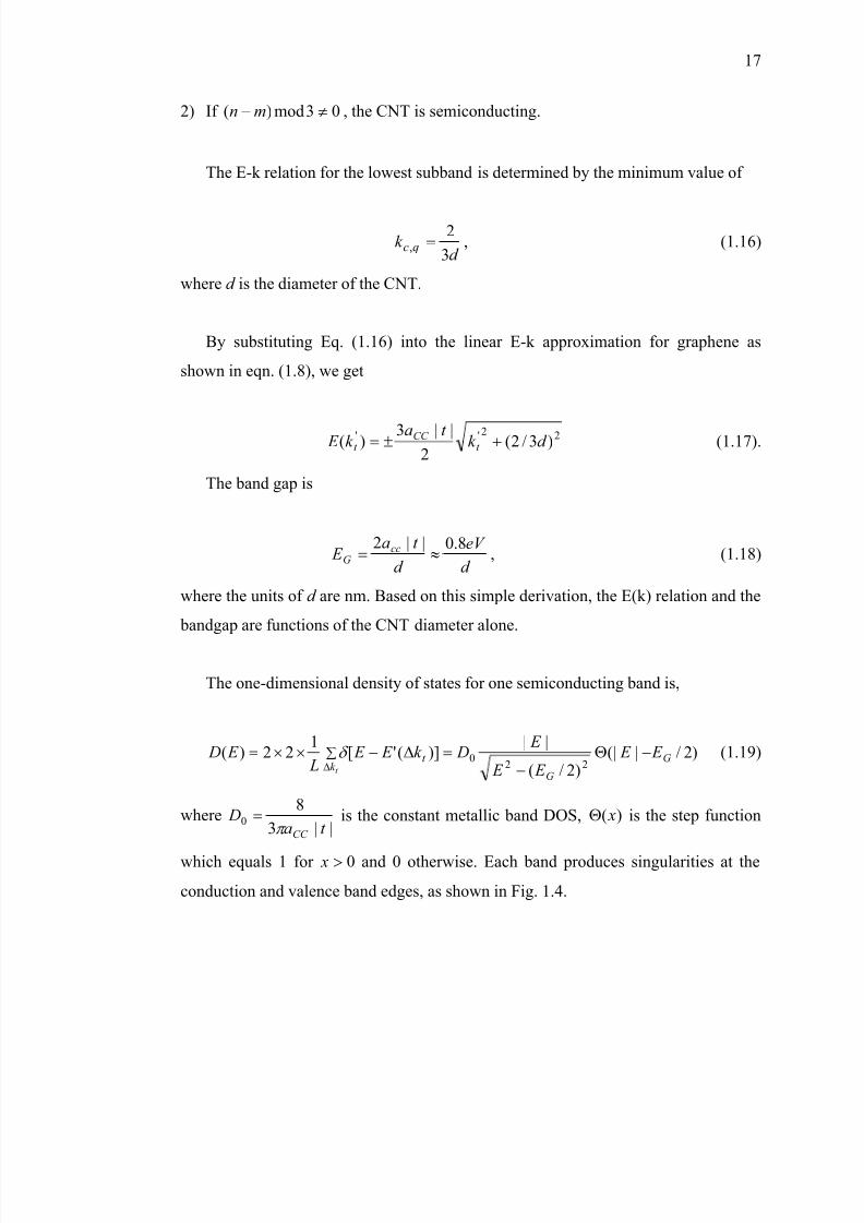
1.2 Carbon Nanotube Basics
1.2.1 Graphene sheet
The nanotube can be conceptually viewed as a rolled-up graphene sheet [6, 15]. A
simple way to calculate the one-dimensional E-k relation of carbon nanotube, which
governs its electronic property, is to quantize the two-dimensional E-k of the graphene
sheet along the circumfencial direction of the nanotube. Thus the first step to calculate
the nanotube E-k is to calculate the band structure of the graphene sheet.
Fig. 1.2 Carbon nanotubes can be viewed as a rolled graphene sheet. The periodicboundary condition only allows quantized wave vectors around the circumferential
direction, which generates one-dimensional bands for carbon nanotubes [6].
With the scaling limit of conventional silicon transistors in sight, there is rapidly
growing interest in nanowire transistors with one-dimensional channels, such as carbon
nanotube transistors [5, 6] and silicon nanowire transistors [18-21]. Due to the one-
dimensional channel geometry, the electrostatics of nanowire devices can be quite
different from bulk silicon devices. Previous studies of carbon nanotube p/n junctions and
metal/semiconductor junctions demonstrated unique properties of nanotube junctions [22,
23]. For example, the charge transfer into the nanowire channel from the metal contacts
(or heavily doped semiconductor contacts) can be significant [23, 24].
In this paper, we extend previous studies by looking at the dependence of the charge
transfer on the metal/semiconductor Schottky barrier height, the insulator dielectric
constant, and the metal contact geometry. We show that if an intrinsic nanowire is
attached to bulk metal contacts at two ends, large charge transfer can be achieved if theSchottky barrier is low and the insulator dielectric constant is high. If, however, the
intrinsic nanowire is attached to one-dimensional metal contacts, the charge density on
the nanowire depends critically on the electrostatic environment rather than the properties
of the metal contacts. Reducing the gate oxide thickness and the contact size decreases
the distance over which the source/drain field penetrates into the nanowire channel and
can, therefore, help to suppress the short channel effects and improve the transistor
Fig. 2.1 The modeled, coaxially gated carbon nanotube transistor. The intrinsic nanotubechannel has a diameter of 1.4nm and the gate work function is zero. The cylindricalcoordinates for solving the Poisson equation is also shown.
2.2 Approach
We simulated the coaxially gated carbon nanotube transistor shown in Fig. 2.1.
Although the calculations are for carbon nanotube transistors, the general conclusion
should apply to other nanowire transistors with one-dimensional channels. The
equilibrium band profile and charge density were obtained by solving the Poisson
equation in cylindrical coordinates self-consistently with the equilibrium carrier statistics
of the carbon nanotube. The charge density per unit length on the nanotube, QL (z), is
calculated by integrating the “universal” nanotube density-of-states (DOS) [17], )(E D ,
over all energies,
))](~
)[(sgn()()sgn()()( ∫ +∞
∞−−⋅⋅−= z E E E f E DE dE ez Q F L , (2.1)
where e is the electron charge, )sgn(E is the sign function, and )()(
~z E E z E mF F −= is
the Fermi energy level minus the middle gap energy of the nanotube, )(z E m . Since the
source/drain electrodes are grounded, the Fermi level is set to zero, 0=F E . The
nanotube middle gap energy is computed from the electrostatic potential at the nanotube
intrinsic channel due to the work function difference between the metal and the
semiconductor. Fig. 2.2c plots the conduction bands, and Fig. 2.2d plots the charge
densities in the unit of electron per atom for the bulk Si and nanotube channel. Compared
to the bulk Si channel, the barrier in the nanotube is much lower, and the charge density
is much higher. Although the nanotube is mµ 3 long, the charge density at the center of
the tube is still as high as 10-4e/atom , about 5 orders of magnitude higher than that of the
bulk Si in terms of electron fraction. As the result, the carbon nanotube channel is more
conductive.
Fig.2.2 The schematic plots for (a) a bulk Si structure where the cross-sectional area isassumed to be large (b) a carbon nanotube channel between bulk metal electrodes. The
Schottky barrier heights for electrons are zero. (c) The conduction band edge and (d) theelectron density in the units of doping fraction. Results for the bulk Si structure are
shown as dashed lines and for nanotube as solid lines.
where C ins is the electrostatic capacitance per unit length between the nanotube and the
bulk contacts. The electron density due to the charge transfer from the bulk contacts can
be obtained from eqns. (2.3) and (2.4) as
Qins C C
eU xn
/1/1
/)(
20
+= , (2.5)
where the quantum capacitance [27] is defined as, DeC Q2= , which is proportional to
the average DOS of the nanotube. Equation (2.5) can be interpreted in a simple way. The
bulk electrodes modulate the charge density of the nanotube through an insulator
capacitor, insC , which is in series with the quantum capacitance of the nanotube.
Fig.2.3 The electron density (the dashed line) and hole density (the solid line) at thecenter of the 3 mµ -long CNT (in Fig. 2.2b) vs. the Schottky barrier height for electrons,
bnφ , and that for holes, bpφ . The left axis shows the charge density in the unit of number
of electrons (holes) per unit length and the right axis shows the same quantity in the unitof charge fraction.
Fig.2.5. Contact geometry. A mµ 3 -long CNT between (a) the bulk contacts and (b) theone-dimensional wire contacts. The tube diameter is 1.4nm. and Schottky barrier heights
for electrons are zero. A coaxial gate far away with a mµ 30 radius is grounded. The
workfunction of the gate metal equals to the semiconductor affinity plus the band gap, sothat the gate tends to dope the CNT to p-type. (c) The band profile (a). (d) The band
The importance of charge transfer into the carbon nanotube channel by one-
dimensional metal contacts has been previously discussed in [23]. We, however, reached
the same conclusion that charge transfer into the one-dimensional channel is significant
for a different contact geometry (the bulk contacts). We also explored the one-
dimensional contacts. In this case, the results are quite different from bulk contacts. The
charge density of the nanotube channel is critically determined by the electrostatic
environment (i.e., the potential and location of nearby bulk contacts) rather than the
metal-contact properties, as will be discussed in detail next.
Fig. 2.5 illustrates the important role of the contact geometry. We simulated: 1) a
CNT between grounded bulk contacts as shown in Fig. 2.5a, and 2) a CNT between
grounded wire contacts as shown in Fig. 2.5b. In both cases, the tube length is mµ 3 and a
grounded, coaxial gate cylinder is far away with a radius of mµ 30 . The S/D contacts
have zero Schottky barrier heights for electrons thus tend to dope the tube n-type, while
the gate has a high work function and zero barrier height for holes thus tends to modulate
the tube to p-type. For the bulk contact case, the whole tube is doped to n-type by bulk
contacts and the charge density on the tube is independent of the voltage on the gate
cylinder. In contrast, for the wire contacts, the tube is lightly modulated to p-type and the
charge density on the tube is very sensitive to the potential on the gate, although it is far away. The results shown in Fig. 2.5 can be explained as follows. For the bulk contacts,
because the gate cylinder is far away, the bulk contacts at the ends collect all field lines
and image all charge on the tube, as shown in Fig. 5a. For the wire contacts, however, the
potential produced by the charge on the one-dimensional wire decays rapidly with
distance, thus several nanometer away from the metal/semiconductor interface, the wire
contacts have little effects. On the other hand, the capacitance between the gate cylinder
and the tube decays slowly (logarithmically) with the tube radius, thus several nanometer
away from the metal/semiconductor interface, the charge on the tube images on the gate
rather than the wire contacts nearby. As a result, the charge density is determined by the
potential on the gate. The charge density on the nanotube channel is essentially
One consequence of the significant charge transfer is that nanowire transistors with
large gate underlap can still operate. Fig. 2.6a shows a coaxially gated CNTFET with a
500nm gate underlap and the bulk electrodes. Fig. 2.6b plots the conduction band profile
at 0=GV and 0.3V. At the off state ( V V G 0= ), a large barrier is created in the channel
and the transistor is turned off. At the on-state, ( V V G 3.0= ), the barrier under the gate is
pushed down. Because the low dimensional charge on the ungated nanotube doesn’t
effectively screen the potential produced by the gate and S/D electrodes, the potential at
the ungated region is close to the Laplace potential produced by the source and gate
electrodes. The conduction band edge is approximately linear in the ungated region. If the
Schottky barrier height between S/D and the channel is ~50meV, the barrier height at the
ungated region at the on-state is low enough to deliver an on-current of ~1 Aµ . This
mechanism provides a possible explanation for the operation of the n-type CNTFET in a
recent experiment by Javey et al. [11], in which a n-type CNTFET with large, intrinsic
gate underlaps still had a good on-off ratio.
One concern about the nanowire transistors with low meta/CNT Schottky barriers is
that due to the significant charge transfer, it might be difficult to turn off the transistor.
To examine this concern, we simulated the coaxially gated CNTFET as shown in Fig. 7a
with different gate oxide thickness. Fig. 2.7b, which plots the equilibrium band profile,
shows that when the gate oxide thickness is the same as the channel length, the
source/drain field penetrates into the channel the channel and the transistor cannot be
turned off. When the gate oxide is thin, however, the gate still has very good control over
the channel and the transistor is well turned off. By solving the Poisson equation for the
CNTFET in Fig. 2.7a, the length by which the drain field penetrates into the channel (the
scaling length [28]) is estimated to be the radius of the cylindrical gate, GR~Λ . If theratio between the channel length and the gate oxide thickness is large, the transistor can
Fig. 2.6. (a) A coaxially gated CNTFET with bulk electrodes (with a radius of 500nm)and a large gate underlap. (b) The conduction band profile at VG=0V and 0.3V. The
metal/CNT barrier height for electrons is 50meV, the ZrO2 gate oxide thickness 8nm, thetube diameter is1.4nm, the gate length is 2 mµ , and the gate underlap is 500nm.
Fig. 2.7. (a) A coaxially gated CNTFET with a 20nm-long, intrinsic channel. Thesource/drain radius, RC , is equal to the oxide thickness. The metal/CNT barrier height for
electrons is zero, the tube diameter is 1.4nm and the dielectric constant of the gateinsulator is 25=ε (b) the equilibrium conduction band edge at V G=0 for the gate oxide
Fig. 2.8. The equilibrium conduction band edge at V G=0 for the CNTFET as shown inFig., 2.7a. The gate oxide thickness is kept constant at 20nm and the source/drain contact
radius, RC =0.7nm, 8nm, and 20nm.
Another way to reduce the penetration of the lateral field is to reduce the size of the
source/drain contact. Fig. 2.8, which plots the equilibrium band profile for the CNTFET
(in Fig. 2.7a) with 20nm-thick gate oxide and different contact radius, shows that the
screening length for lateral fields from S/D contacts decreases when the contact radius
decreases. In the limit when the source/drain electrodes are reduced to wires with the
same radius as the tube, the transistor can be well turned off, although the oxide thickness
is large. As discussed earlier, the reason it that the potential produced by wire contacts
decays rapidly with distance. Improving transistor performance by engineering contacts
has been discussed by Heinze et al, when they study the Schottky barrier CNTFETs.Smaller contacts produce thinner Schottky barriers and improve the transistor
3. SIMULATING QUANTUM TRANSPORT IN BALLISIT CARBON
NANOTUBES
3.1 Introduction
Carbon nanotubes show promise for applications in future electronic systems, and the
performance of carbon nanotube transistors, in particular, has been rapidly advancing [12,
14]. From a scientific perspective, carbon nanotube electronics offers a model system in
which to explore and understand the effects of detailed microstructure of contacts,
interfaces, and defects. It is also an opportunity to develop the theory and computational
techniques for the atomistic simulation of small electronic devices in general. A detailed
treatment of carbon nanotube electronics requires an atomistic description of the
nanotube along with a quantum mechanical treatment of electron transport, both ballistic
and with the effects of dissipative scattering included. As shown in Fig. 3.1, even for this
simple system, multi-scale methods are essential. Metal/nanotube contacts,
nanotube/dielectric interfaces, and defects require a rigorous, ab initio treatment, but to
treat an entire device, simpler, pz orbital descriptions must be used. Techniques connectdifferent descriptions used for different regions of the device will need to be developed
(e.g. the ab initio basis functions for the metal/nanotube contacts must be connected to
the semi-empirical basis functions for the device itself). For extensive device
optimization, continuum, effective mass level models may be necessary, and methods to
relate the phenomenological parameters in those approaches to the atomistic models must
be developed. For circuit simulation, even simpler, analytical models are needed, and
efficient techniques for extracting circuit models from physically detailed models must be
Fig.3.1 An illustration of how continuum, ab initio, atomistic and semi-empiricalatomistic models will be combined in a multi-scale description of a carbon nanotube
electronic device.
Our purpose in this paper is to describe the status of our work to develop a
comprehensive, multi-scale simulation capability for electronic devices. We will focus
on our initial effort that make use of a semi-empirical, pz orbital description, and discuss
briefly the challenges to be addressed in connecting this work to ab initio simulations, to
continuum device simulations, and to circuit models. The approach has already
demonstrated its usefulness in analyzing recent experimental data, suggesting
experiments, and in exploring device possibilities [9].
3.2. Review of the NEGF Formalism
A carbon nanotube can be viewed as a rolled-up sheet of graphene with a diameter
typically between one and two nanometers. The nanotube can be either metallic or
semiconducting, depending on how it is rolled up from the graphene sheet (i.e. depending
on its chirality) [15]. Semiconducting nanotubes are suitable for transistors. In order to
correctly treat carbon nanotube transistors, strong quantum confinement around the tube
circumferential direction, quantum tunneling through Schottky barriers at the
metal/nanotube contacts, and quantum tunneling and reflection at barriers in nanotube
channel need to be considered. The non-equilibrium Green’s function (NEGF) formalism,
which solves Schrödinger equation under non-equilibrium conditions and can treat
coupling to contacts and dissipative scattering process, provides a sound basis for
quantum device simulations [29]. The NEGF simulation approach has demonstrated its
usefulness for simulating nanoscale transistors from conventional Si MOSFETs [30],
MOSFETs with novel channel materials [31], to CNTFETs [9, 32], and molecular
transistors [33]. In this section, we give brief summary of the NEGF simulation
procedure. For a more thorough description of the technique, see [34].
Fig.3.2 The generic transistor with a molecule or device channel connected to the sourceand drain contacts. The source-drain current is modulated by a third electrode, the gate.
The quantities in the NEGF calculation are also shown.
( )))]((sgn[),( FDN D E E z E E f z E D −−+ , (3.2)
where sgn(E ) is the sign function, and DFS E , is the source (drain) Fermi level. For a
self-consistent solution, the NEGF transport equation is solved with iteratively the
Poisson equation until self-consistency is achieved after which the source-drain current is
computed from
∫ −= dE E f E f E T h
eI DS )]()()[(
4(3.3)
where )GG(Trace)( 21 += E T is the source/drain transmission and the extra factor of two
comes from the valley degeneracy in the carbon nanotube energy band structure.
The computationally expensive part of the NEGF simulation is finding the retarded
Green’s function, according to eqn. (3.1), which requires the inversion of a matrix for
each energy grid point. The straightforward way is to explicitly invert the matrix, whose
size is the size of the basis set. This, however, is impractical for an atomistic simulation
of a nanotube transistor. In the ballistic limit, the problem is simplified because only afew columns of the Greens’s function are needed. Still, reducing the size of the
Hamiltonian matrix and developing computationally efficient approaches are of great
importance for an atomistic simulation.
3.3. Atomistic NEGF Treatment of Electron Transport in Carbon Nanotubes
3.3.1 Real space approach
In this section, we describe an NEGF simulation of ballistic CNTFETs using a real
space basis. The first step is to identify a set of atomistic orbitals adequate to describe the
Fig.3.3 The schematic diagram of a (n, 0) zigzag nanotube (n = 6 in this case). The circlesare the A-type carbon atom sublattice, and the triangles are the B-type carbon atom
sublattice. The coordinate system is also shown: c is the circumferential direction, and x
transport. Modes with their band edges well above or below the source and drain Fermi
levels are unimportant to carrier transports. The E (k ) relation for the qth mode as
computed from eqn. (3.10) is E (k ) = ± t 2 + b2q2 + 2tb2q cos 3kaCC 2( ), where acc ≈ 1.42Å is
the C-C bonding distance. The qth mode produces a conduction band and a valence bandwith symmetric E (k ) , and a band gap of ( ) nqt E g π cos1||2 += . When 03mod =n ,
the lowest subband index is 3/2nq = , which results in t b q −=2 and a zero band gap.
Otherwise, the nanotube is semiconducting and the lowest subband index is the integer
closest to 3/2n . By retaining only those modes whose carrier population changes with
device bias or operating temperature, the size of the problem is significantly reduced.
(a)
(b)
Fig.3. 4(a) The real space 2D lattice of the (n, 0) zigzag nanotube (b) The uncoupled, 1D
mode space lattices. A basis transformation on the real space lattice of (a) transforms theproblem to the M one-dimensional problems, where M labels a specific k C .
The mode space source and drain self-energies can be computed using the same
recursive relation for the surface Green’s functions already discussed in Appendix A. The
details are provided in Appendix B. The structure of the self energy matrices is the same
as in eqn. (3.7) except that Σ11 (and ΣNCNC for the drain self energy) are numbers rather
than n x n submatrices. After obtaining the Hamiltonian matrix and contact self energies,
the retarded Green’s function is computed. Because the Hamiltonian matrix for a mode
is tridiagonal and only a small part of the retarded Green’s function is needed for the
purpose of computing charge density and current at the ballistic limit, the recursive
algorithm [37] or Gaussian elimination, rather than explicit matrix inversion, is used to
compute the retarded Green’s function.
3.4. Phenomenological Treatment of Metal/CNT junctions
In carbon nanotube transistors, the metal source and drain are typically attached
directly to the intrinsic nanotube channel, and the gate modulates the source-drain current
by changing the transmission through the Schottky barrier at the source end of the
channel. To properly simulate such devices, the metal/CNT junction must be treated
quantum mechanically. We currently treat this problem phenomenologically by definingan appropriate self-energy. Note that the self-energies defined in Sec. 3 do not apply here
– they assume that carriers enter and leave the device without the need to tunnel through
any barriers at the contact. As shown in Fig. 3.5, the phenomenological self energy must
contain two parameters, one to describe the barrier height and another the density of
metal-induced gap states (MIGS). Our approach mimics the effect of a real metal contact
by specifying its work function and by injecting a continuous density of states near the
Fermi level. This approach has proven useful in understanding transistor operations of
Fig.3.5 (a) The metal-carbon nanotube junction. (b) The band diagram of the junction.EC, EV and Em are the conduction band edge, the valence band edge, and the middle
gap energy in the nanotube, respectively. EFm is the metal Fermi level, and bnφ is theSchottky barrier height for electrons.
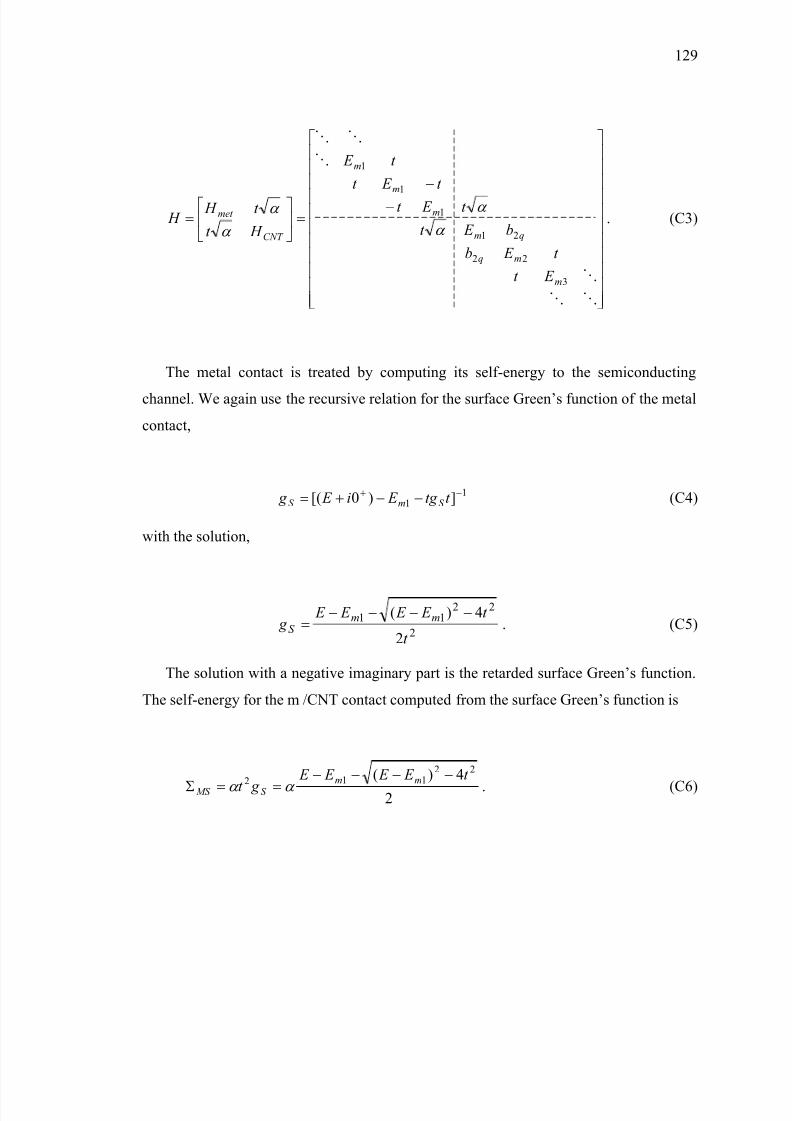
The phenomenological treatment is described in Appendix C. In brief, each
semiconducting mode in the semiconducting zigzag nanotube is coupled at the M/CNT
interface to a mode of a metallic zigzag CNT. As shown in Appendix C, Σ11 in eqn. (3.7)
becomes
2
4)( 22112 t E E E E
g t mm
S MS
−−−−==Σ α α . (3.11)
The coupling is described by two parameters. The first parameter is boφ , the
Schottky barrier height for electrons without the presence of the interface states, which
describes the band discontinuity at the interface and provides the value for 1mE , the mid-
gap energy of the CNT at the interface. ( 2/01 g bFmm E E E −+= φ , where FmE is the
metal Fermi level and g E is the CNT band gap.) The second parameter is the tight-
binding parameter, α, between the semiconducting and the metallic mode ( 10 ≤<α ),
direction) and the radial direction (r -direction) as shown in Fig. 3.6. Poisson’s equation
is written as
ρ ε ez r E m −=∇ ),(2 , (3.12)
where mE is defined as the vacuum energy level minus the work function of an intrinsic
nanotube, and is exactly the middle gap energy for the grid points on the tube surface,
and ρ is the charge density, which is non-zero only for grid points on the tube surface.
The boundary condition applied at 0=r is that the electric field along the r-direction is
zero [39],
0| 0 ==r r ε . (3.13)
The potential at the gate electrode is known, so using the Fermi level of a grounded
electrode as the zero energy, the electron potential at the gate electrode is,
Fig.3.6 The modeled, coaxially gated carbon nanotube transistor with heavily-doped,semi-infinite nanotubes as the source/drain contacts. The channel is intrinsic and the gatelength equals the channel length. Also shown are the simulated area, the simulation gridand the cylindrical coordinate system used for solving the Poisson equation. The dashed
rectangular area shows the element used to discretize the Poisson equation at (xi, r j).
Equation (3.16) is linear and mathematically easy to solve, but the convergence of the
quantum transport and the linear Poisson equation is poor [26]. A non-linear Poisson
equation, which relates the charge density to the potential through a non-linear dummy
function, has been proven to be very useful in improving the convergence. The non-linear
dummy function relating the charge density and the potential should be as close to the
physical relation determined by carrier transport equation as possible for better
convergence. Typically, semiclassical, equilibrium carrier statistics with a dummy quasi
Fermi level are used as the dummy function. The non-linear Poisson equation takes the
charge density computed by the transport equation as the input, and converts the charge
density to a quasi Fermi level using the dummy function. Then the non-linear Poisson
equation is solved for the potential by Newton-Ralphson iteration. Details of the non-
linear Poisson solver can be found in [26].
Fig.3.7 The self-consistent iteration between the NEGF transport and the electrostaticPoisson equation. These two equations are iteratively solved until self-consistency is
achieved. Then the current is computed using the self-consistent potential.
The simulation methods discussed in the previous sections have proven useful in
several recent transistor studies [9]. The purpose of this section is to show some simpleexamples to demonstrate that: i) quantum effects are captured, ii) the mode space
approach is valid when potential is uniform around the tube, and iii) the metal/CNT
junction can be treated by our phenomenological self energy.
We first simulate a coaxially gated, MOSFET-like CNTFET as shown in Fig. 3.6.
The transistor channel is a (25,0) intrinsic CNT, which results in a band gap of ~0.42eV
and a diameter of ~2nm. The nanotube length is ~50nm, consisting of ~ 4102.1 × carbon
atoms. A self-consistent Poisson-NEGF simulation in the real space (using the recursive
algorithm for computer the Green’s function) is performed. Fig. 3.8a shows the energy-
resolved local-density-of-states (LDOS), and the energy band profile. The band gap
region with extremely low LDOS (darker in the grayscale plot) can be clearly identified.
Due to the existence of the barriers, the source/drain incident wave is reflected and the
quantum interference pattern between the incident and reflected waves is apparent. A
quantum well is formed in the valence band of the channel, and the 1st and 2nd confined
states with one or two LDOS maxima, respectively, can be clearly seen. The band edge of
the second subband is also observed. Figure 3.8b shows the energy resolved electron
density (electron density spectrum), which is obtained by filling the LDOS with the
source or drain Fermi level. The bandgap, quantum interference, quantum confinement,
Fig.3.8(a) The local-density-of-states (LDOS) and (b) the electron density spectrumcomputed by the real space approach at VG=0.25V and VD=0.4V. The modeled transistor is shown in Fig. 7a. The nanotube is a (25,0) CNT with a diameter d~2nm and bandgap
Next, we explore the validity of the mode space approach by comparing the results of
the real space approach to those of the mode space approach. The mode space approach
theoretically should exactly reproduce the results of the real space approach when the
potential is invariant around the tube, and a sufficient number of modes is included in the
mode space simulation. A CNTFET as shown in Fig. 3.6 with a (13,0) nanotube channel,
which results in a band gap of ~0.83eV and a diameter of ~1nm, is simulated. The
carbon nanotube length is ~50nm, consisting of ~6000 carbon atoms. Because the third
subband is ~1eV away from the lowest subband and the applied bias is 4.0≤ V, only the
lowest two subbands are treated in the mode space simulation. The Hamiltonian matrix
for the lowest subband is small ( 500500~ × ), and computing the Green’s function for a
subband using the recursive algorithm is fast even on a single CPU PC. Figure 3.9, which
compares the I-V characteristics of the real space and mode space approaches, shows that
the mode space simulation excellently reproduces the results of the real space approach.
Figure 3.10, which plots the band profile and the charge density at on-state, again shows
that the mode space approach excellently reproduces the results from the real space
approach results. The good agreement between the real and mode space approach results
from the equal potential around the tube direction when it’s coaxially gated. The mode
space is highly advantageous in reducing the computational burden, and it is valid whenthe potential variation around the tube is much smaller than the spacing between the
Fig.3.11(a) The coaxially gated Schottky barrier carbon nanotube transistor with anintrinsic nanotube channel directly attached to metal source and drain contacts. The
nanotube channel is a (13,0) zigzag CNT with a diameter d~1nm and band gapEg~0.83eV. The gate insulator is a 2nm-thick ZrO2. (b) The local-density-of-states
(LDOS) at 4.0== GD V V V, which clearly shows tunneling through the Schottky barrier
at the source end of the channel, and metal induced gap states (MIGS) at the metal/CNTinterfaces.
The semi-empirical approach described in this paper is only one part of a multi-scale
hierarchy shown in Fig. 3.1. More rigorous, ab initio methods are needed to treat themetal/CNT interface properly. Such simulations would allow first principles calculations
of the barrier height and the MIGS, two parameters that we now treat as
phenomenological. Such simulations may also provide useful insights into how to
produce ohmic, rather than Schottky barrier, contacts when desired. The
phenomenological model, however, is well-suited for device-scale simulations because of
its computational efficiency. One approach to this multi-scale challenge is to relate the
phenomenological parameters for the metal/nanotube contacts in the semi-empirical
approach described in this paper to detailed atomistic simulations of the contact. In such
an approach, the semi-empirical model would stand alone and be related to separate, ab
initio simulations. Another possibility is the domain decomposition approach sketch in
Fig. 3.1. In this approach, the key challenge is to connect the two regions, described with
much different sets of basis functions, through the self-energies. This “mixed basis set
approach” is already being applied to problems involving molecules on silicon contacts
and is being investigate for the metal/nanotube contact as well.
The approach described in this paper assumes ballistic transport, but scattering by
phonon emission is likely to be a factor in devices under realistic operating voltages [41-
44]. There is a clear prescription for treating the electron-phonon interaction within the
NEGF formalism [29, 34], but the computational burden increases rapidly. It is likely,
therefore, that semiclassical, continuum approaches like those used to treat
semiconductor devices by Monte Carlo simulation [45] will be needed when a detailed
treatment of the electron-phonon coupling is necessary. NEGF simulation is the method
of choice when quantum transport is the dominant factor, and phenomenological
treatments of scattering can be used [46, 47]. Semiclassical approaches are the method of
choice when scattering dominates, and phenomenological quantum corrections can be
made.
Finally, work at the device level needs to be coupled to circuit level models so thatthe system level implications of novel devices can be readily explored. Existing
approaches may or may not be adequate. CNTFETs, for example, should operate near the
ballistic limit, and it is not clear that traditional MOSFET models, which were developed
for the scattering-dominated regime, can be extended to quasi-ballistic transistors.
Recently, a new circuit model for ballistic CNTFETs has been developed [48]. The more
general question of how circuit models for new exploratory devices can be rapidly
developed is an important one to address.
3.8. Conclusions
Methods for the NEGF/Poisson simulation of carbon nanotube transistors were
discussed and illustrated. The real space approach, which uses one pz orbital per carbon
atom as the basis, achieves atomistic resolution for quantities of interest. Significant
computational saving can be achieved by using the mode space approach, whichperforms a basis transformation around the nanotube circumferential direction and
transforms the 2D nanotube lattice to decoupled 1D mode space lattices. Each mode in
the mode space approach describes one conduction subband and its corresponding
valence subband, and atomistic resolution along the transport direction is retained. The
simulation methods discussed in this paper have been applied to several transistor studies
with the purpose of understanding experiments and exploring device physics [9]. Finally,
the need to complement this semi-empirical device level model with higher level circuit
models and lower level ab initio models was discussed.
Carbon nanotube field-effect transistors (CNTFETs) with promising device
characteristics have recently been demonstrated [13, 14, 49, 50], so the question of the
ultimate device performance capability and minimum device size that might be
achievable from an optimized technology becomes important. A recent scaling study of
Schottky barrier (SB) CNTFETs by Heinze et al. [51] examined the role of scaling the
gate oxide thickness down and the dielectric constant up. That study found that the device
performance depends in an unexpected way (as compared to a silicon MOSFET) on the
gate oxide thickness and dielectric constant. In a very recent study, the issue of drain
voltage scaling has been considered [10]. In this paper, we extend previous work by
using a coupled Poisson-quantum transport model to treat the charge in the nanotube self-
consistently. A comprehensive study of CNTFET scaling issues is performed to examine
the role of gate insulator thickness and dielectric constant, nanotube diameter, Schottky
barrier height, drain voltage, and channel length. In contrast to SB CNTFETs with thick gate oxides, SB CNTFETs with thin gate oxides show very strong ambipolar I-V
characteristics, even if the barrier heights for electrons and holes are highly asymmetric.
The ultimate scaling limit for the channel length imposed by source-drain tunneling is
established. The nanotube diameter and drain voltage are shown to have a strong
influence on the leakage current. In contrast to a previous study [51] that examined the
subthreshold and near threshold regions, we find that increasing the gate dielectric
constant improves device performance (the on-current).
In this study, we restrict our attention to Schottky barrier CNTFETs, which operate
by modulating the tunneling current at the source contact. (SB CNTFETs are common in
experiments at this stage [7, 8].) Note, however, that there are recent reports that
CNTFETs without Schottky barriers, which operate more like MOSFETs, can be realized
[13]. We assume ballistic transport and solve the Schrödinger equation self-consistently
with the Poisson equation. Because our interest is ultimate limits, we assume a coaxial
geometry, rather than the planar geometry of the actual devices that have been reported.
The coaxial geometry provides the best electrostatic control by the gate and, therefore,
the minimum channel length for electrostatic consideration [39, 52]. A zigzag nanotube
is assumed, and an atomistic description in terms of pz orbitals is used. Our assumption of
ballistic transport is a reasonable one that facilitates simulations [13, 53, 54], but it is not
central to this paper. We focus here on understand the device physics of ambipolar
conduction in SB CNTFETs and do not expect the conclusions to depend on whether
transport is ballistic or not.
4.2 Approach
To investigate the performance of aggressively scaled CNTFETs, we simulated a
coaxially gated CNTFET with a 15nm ballistic channel, as shown in Fig. 4.1 at room
temperature (T=300K). The nominal device has a 2nm ZrO2 gate oxide (a high-K gate
insulator of this type has been experimentally demonstrated [55]). The diameter of the(13, 0) nanotube is d ≈ 1 nm, which results in a bandgap of E g ≈ 0.83 eV . A power supply
voltage of 0.4V is assumed, according to the value specified for the 10nm scale MOSFET
in ITRS roadmap [56]. The device parameters here are the nominal ones; we explore
various issues by varying these parameters.
Carbon nanotube field-effect transistors were simulated by solving the Schrödinger
equation using the non-equilibrium Green’s function (NEGF) formalism [29, 34, 57] self-
consistently with the Poisson equation. Ballistic transport was assumed. An atomistic
description of the nanotube using a tight binding Hamiltonian with an atomistic (pz
orbital) basis was used. The atomistic treatment was computationally expensive, but
significant computational savings were achieved by the mode space approach [30].
Because the carbon nanotube is coaxially gated, the eigenstates around the tube
circumferential direction (modes) are plane waves with wave vectors satisfying the
periodic boundary conditions. The two-dimensional nanotube lattice of a (n, 0) zigzag
CNT was transformed to n decoupled one-dimensional modes by doing a basis transform
from the real space to the mode space in the circumferential direction (essentially Fourier
transform). Under typical bias conditions, the few modes that are relevant to electronic
transport are treated.
Fig.4.1 The modeled CNTFET with a coaxial gate. The gate length is the same as thesource to drain spacing; the nominal value is 15nm. A 2nm-thick ZrO2 gate insulator and
a (13,0) zigzag nanotube (with the diameter d~1nm and the band gap E g ~0.8eV ) areassumed.
The mode space approach reduces computation significantly yet retains atomistic
resolution along the transport direction. For the ith mode, the charge density is computed
by integrating the local density-of-states (LDOS) over energy,
( )∫ +∞∞− −−−⋅−= ))]((sgn[),()](sgn[)()( FS N iS N i E E z E E f z E Dz E E dE ez Q
( )))]((sgn[),( FDN iD E E z E E f z E D −−+ , (4.1)
where e is the electron charge,sgn(E ) is the sign function, DFS E , is the source (drain)
Fermi level, and DiS ,D (E ,z )is the LDOS due to the source (drain) contact as computed by
the NEGF method. Because the nanotube conduction and valence bands are symmetric,
the charge neutrality level, E (z ) , lies at the middle of band gap [35].
The Schottky barriers at the metal/CNT interfaces were treated phenomenologically.
To mimic the continuous states injected from metal to the semiconducing nanotube
modes, each semiconducting mode is coupled to the metallic mode of metallic zigzag
CNTs at the M/CNT interface with the coupling described by two parameters. The first
one is the band discontinuity at the interface, which is the Schottky barrier height when
there are no interface states. The second parameter is the tight-binding parameter between
the semiconducting and the metallic mode, which determines to the density of metal-
induced-gap-states (MIGS). This simple model describes the interface at a similar level
as the M/CNT models in literature with the band discontinuity and density of interface
states treated as input parameters [22].
A 2D Poisson equation is solved to update the charge neutrality level in eqn (4.1),
)2/,()( d r z ez E N =−= φ , where d is the nanotube diameter and )(z φ is the electrostatic
potential,
ε
ρ φ −=∇ ),(2 r z . (4.2)
The potentials at source/drain and gate electrodes are fixed as the boundary conditions,
and the gate flat band voltage was assumed to be zero for simplicity. (In practice, itwould depend on the gate workfunction.) In order to treat an arbitrary charge distribution
on the nanotube channel, the Poisson equation (eqn. (2)) is solved by the method of
moments [25]. The iteration between the atomistic quantum transport equation and the
electrostatic equation continues until self-consistency is achieved, (a non-linear form of
eqn (2) is used to improve the iteration convergence [26]), then the source-drain ballistic
current is computed by
∫ −−−⋅= )]()()[(4
FDFS E E f E E f E T dE h
eI , (4.3)
where )(E T is the source-drain transmission calculated by the NEGF formalism [29]. The
We begin by simulating the nominal device and display the resulting log ID vs. VGS characteristic in Fig. 4.2a. For the CNTFET with the metal Fermi level at the middle of
the bandgap, the transistor is ambipolar, showing symmetric electron and hole conduction
(see the solid line in Fig. 4.2a). The minimum current occurs when the gate voltage is
one-half the drain voltage at which the gate-to-source voltage equals the drain-to-gate
voltage, and the conduction and valence band profiles are symmetric (see the solid line in
Fig. 4.2b). Radosavljevic et al. observed similar behavior, and this bias is also the
optimum bias for observing optical emission in CNTFETs [58, 59]. Several questions
will be addressed in the remainder of this paper. What controls the minimum current, the
on current, and the subthreshold swing? Can conduction of one type be suppressed so
that SB CNTFETs can be used in conventional CMOS digital circuits? How does device
performance depend on the nanotube diameter, power supply, gate insulator thickness
and dielectric constant, and the channel length?
Figure 4.2 shows the effect of the metal/CNT barrier height on the ID-VGS characteristics for the nominal device with a thin (2nm) high-K (25) gate dielectric.
Reducing the barrier height for electrons to zero increases the electron conduction current
for V GS >V DS /2 and decreases the hole current for V GS < V DS /2. The I D – V GS
characteristic, however, remains approximately symmetrical; the dash-dot line in Fig.
4.2b explains why. Although the barrier height for holes is high when φ bn = 0 ( g bp E =φ )
and barriers to hole conduction exist at both the source and drain electrodes, the barriers
are thin. (The thickness of the Schottky barrier is approximately the thickness of the gateoxide [60]). The thin barriers are quite transparent at negative gate voltages. The
observation that CNTFETs with thin gate oxide tend to be ambipolar with nearly
symmetrical characteristics is consistent with recent experiments [14].
Fig.4.2 Transistor characteristics when the gate oxide is thin. (a) ID vs. VG characteristicsfor the nominal CNTFET (as shown in Fig. 4.1) with three different barrier heights. The
Schottky barrier height for electrons is 0=bnφ for the dash-dot line, 2/g bn E =φ for the
solid line and g bn E =φ for the dashed line. (b) The conduction and valence band profile
at V V G 2.0= . The dash-dot line is for 0=bnφ and the solid line is for 2/g bn E =φ . Theflat band voltage of all transistors is zero.
To further clarify the effect of Schottky barrier height on ambipolar conduction, we
translated the I-V characteristics of CNTFETs in Fig. 4.2 along the x-axis so that the
minimum current ( AI µ 4
106~−
× ) occurred at V V G 0= . (Translating the ID vs. VG
curve along x-axis in this way could be achieved in practice by adjusting the gate work
function). The translated I-V characteristics are shown in Fig. 4.3. In the subthreshold
region, the I-V characteristics of the zero barrier and the mid gap CNTFETs are nearly
identical and the minimum leakage current is similar. It is interesting to note that the
subthreshold swing is close to the ideal value of 60mV/dec for thermal injection over a
barrier, no matter what Schottky barrier height is used. For VGS = VDD, the zero barrier
height CNTFET delivers more on-current, and for VGS = -VDD, it deliver less (hole) on-current that for the mid-gap barrier. The general conclusion, however, is that the results
are surprisingly symmetrical about the minimum current – no matter what the barrier
height is.
Fig.4.3 Shifted ID vs. VG characteristics for the nominal CNTFET (as shown in Fig. 4.1)with the barrier height for electrons 0=bnφ (the solid-dash lines) and 2/g bn E =φ (the
solid lines). The minimal leakage current is shifted to 0=GV by adjusting the flat band
voltage for each transistor. The left axis shows the I-V on log scale and the right axisshows the same curves on linear scale.
The reason for the near-ideal subthreshold swing can be explained as follows. When
the gate oxide is thin, the Schottky barrier is also thin and is essentially transparent to
carriers. The current is, therefore, limited by the thermionic emission over a barrier withthe height of the barrier determined by the conduction (valence) band in the interior of
the channel. Tunneling through the M/S barrier varies with the barrier height and the bias,
but it only plays a minor role (because the barrier is so transparent) compared to the
barrier in the CNT body. Accordingly, the subthreshold swing is relatively independent
of the barrier height, and the best that can be achieved is no better than what could be
obtained in a MOSFET. Above the threshold, the situation is different because the
barrier between the source and the CNT body is very small, so the tunneling resistance
limits the on-current. In this case, the zero barrier contact delivers more on-current.
Things change when the gate insulator is thick. Figure 4.4 shows the ID vs. VG
characteristics of a mid-gap SB CNTFET and a 0=bnφ SB CNTFET with a 40nm-thick
K = 25 gate oxide and 100nm channel length. In striking contrast to the thin oxide case,
the I-V characteristics of these two CNTFETs are quite different. The minimum leakage
current of the zero barrier CNTFET is smaller than for the thin oxide transistor, and theon-off current ratio is much better. The reason is that thicker gate insulators lead to
thicker Schottky barriers so the tunneling resistance plays an important role. For the mid-
gap CNTFET, the current is always limited by the Schottky barrier at the M/S contact,
and the gate fringing field modulates the current by changing the tunneling barrier
thickness. As a result, the subthreshold swing is ~200mV/dec – much larger than the
theoretical minimum [7]. For the zero barrier height CNTFETs, however, current
modulation is achieved by modulating a thermionic barrier inside the CNT body, a
mechanism similar to the conventional MOSFET. As the result, the subthreshold swing
is much smaller, at 90mV/dec. (This value is still larger than the ideal subthreshold
swing of 60mV/dec because of short channel electrostatics and the parasitic capacitance
between the source/drain contact and the channel that is large[31].) Because the SB is
Fig.4.5 Scaling of nanotube diameter . ID vs. VG characteristics at VD=0.4V for the
nominal CNTFET with different nanotube diameter. The solid line with circles is for (13,0) CNT (with d~1nm), the sold line is for (17,0) CNT (with d~1.3nm), and the
dashed line is for (25,0) CNT (with d~2nm). The flat band voltage is zero and the Fermilevel lies in the middle of the band gap for all transistors.
We next examine power supply voltage scaling. Figure 4.6a shows the ID vs. VG
characteristics of the nominal SB CNTFET with three different power supply voltages.
Note that the minimum current increases exponentially with power supply voltage (as
Radosavljevic et al. observed [10]). The reason is that the minimum leakage is achieved
when the effective gate to source voltage is one half of the power supply voltage.
Reducing the power supply voltage reduces the effective gate to source voltage at the
minimum leakage point, thus exponentially reduces the minimal leakage current. Figure
4.6a also shows that the on-current increases with VDD. The off-current vs. on-current for
different power supply voltages is plotted in Fig. 4.6b. The trade-off for reducing the off-
current by lowering the power supply voltage is the degradation of on-current. The
choice of power supply voltage will depend on the type of circuit applications. For a lowpower design, the off-current must be small and the on-off current ratio needs to be large,
which sets an upper limit for the power supply voltage. Although the low power supply
voltage guarantees a small leakage current and large on-off ratio (because for small
power supply voltage, the transistor operates in the exponential portion of the ID vs VG
characteristics), the on-current may still be too small for high-performance applications.
To achieve a large on-current and a reasonable off-current simultaneously, which is
required for high performance applications, the power supply voltage must be large
enough.
Fig.4.6 Scaling of Power supply voltage. (a) ID vs VG characteristics under differentpower supply voltages for the nominal CNTFET (Fig. 4.1) with mid-gap Schottkybarriers. For each power supply voltage, the drain is biased at the power supply voltage,VD=VDD. The off-current is defined at the minimal leakage point (V G,off =V D/2), and the
on-current is defined at DDoff GonG V V V += ,, . (b) The off-current vs. on-current for
Figure 4.7 explores the issue of channel length scaling. In order to establish the
ultimate scaling limit imposed by source-drain tunneling, very thin gate oxide ( nmt ox 2=
for the channel length of 10nm and longer and nmt ox 1= for the channel length of 5nm)
is used to ensure excellent gate controlled electrostatics. Although we assume a mid-gapSchottky barrier height, similar observations apply to other barrier heights. When the
channel length is larger than about 15nm, the I-V characteristics are independent of the
channel length because the channel is ballistic and the quantum tunneling resistance of
the Schottky barrier at the source dominates the total channel resistance. Scaling the
channel length down to 10nm significantly increases the off-current, but the on-off
current ratio still exceeds 100, which is probably acceptable for digital logic. If the
channel length is aggressively scaled down to 5nm, the on-off current ratio decreases to
less than 10 due to significant source-drain quantum tunneling. Compared to Si
MOSFETs with the similar channel lengths, the tunneling leakage of the CNTFET is
more severe, partly due to typically smaller band gap and lighter effective mass for
carriers in the CNT channel. (A parabolic E-k fit the very bottom of the conduction band
of a 1nm diameter CNT gives an effective mass of ~0.08.)
Fig.4.7 Channel length scaling. ID vs. VG characteristics of CNTFETs with differentchannel length. The circles are for channel length nmLch 30= and gate ZrO2 thickness
nmt ox 2= , the dash-dot line for nmLch 15= and nmt ox 2= , the solid line for
nmLch 10= and nmt ox 2= , and the dashed line for nmLch 5= and nmt ox 1= . The flat
band voltage is zero and mid-gap Schottky barriers are assumed for all transistors.
Figure 4.8 explores the role of the gate dielectric constant. A previous study, which
omitted the charge on the nanotube, concluded that simply increasing the gate dielectric
constant everywhere didn’t change the band profile thus had no effect on the I-V
characteristics of SB-CNTFETs [51]. Those conclusions apply below and near threshold.
Figure 4.8, which shows the ID vs. VG characteristics for mid-gap SB-CNTFETs with a
2nm thick oxide and three different dielectric constants, shows that a high- κ gate
insulator does increase the on-current. The inset, which plots the conduction band profiles
for three transistors at the on-state, sheds light on these results. Because the Schottky
barriers are thin (due to thin gate oxide), the charge density inside the tube is high. When
the gate dielectric constant is low, this charge produces a considerable self-consistent
potential. The conduction band floats up, which makes the Schottky barrier thicker and
the conduction band in the interior of the channel higher. Because the tunneling currentexponentially depends on the Schottky barrier thickness, the on-current of transistors with
low gate dielectric constants is smaller. Calculations which omit the charge on the CNT
overestimate the current when the mobile charge is important.
Fig.4.8 Gate dielectric scaling . ID vs. VG characteristics at VD=0.4V for the nominalCNTFET with different gate dielectric constant. The solid line is for 25=oxε , the
dashed line for 4=oxε and the dash-dot line for 1=oxε . The inset shows the
corresponding conduction band profile at VG=0.6V. The flat band voltage is zero andmid-gap Schottky barriers are assumed for all transistors.
The key point of this work, as also pointed out by Radosavljevic et al. [10], is the
central importance of ambipolar conduction in SB CNTFETs when the gate oxide is thin,
as it must be for high-performance transistors. To use such SB CNTFETs in
conventional CMOS circuits, will require careful device design because negative gate to
source voltages, and, therefore, high leakage currents, would result when transistors are
stacked. The results presented in 4.3 shed light on how the leakage and on-current varies
with device parameters such as gate insulator thickness, nanotube diameter, power supply
voltage, etc. It is possible that gate work function engineering could be employed so thatin the bias region of interest, only one branch of the ambipolar I-V is used, but this will
be difficult because VGS < 0 occurs for stacked transistors. Alternatively, one could
explore MOSFET-like devices for which ambipolar conduction would not occur [55].
Finally, we should note that we also examined gate oxide thickness scaling and the
effect of contact geometry. The results were similar to those of previous studies [8] (i.e.
reducing the gate oxide thickness and contact size improves the subthreshold swing) were
observed.
4.5 Conclusions
In summary, scaling issues for SB-CNTFETs were explored by self-consistent,
atomistic scale simulations. Ambipolar conduction was found to be an important featurethat must be carefully considered in transistor design. The minimum subthreshold swing
is 60 mV/dec., just as it is for a MOSFET. The scaling limit for CNTFETs imposed by
source-drain tunneling is between 5nm and 10nm and is determined by the small band
gap and strong wave behavior of carriers in CNTs. CNTFETs, therefore, offer no scaling
5. ANALYSIS OF NEAR BALLISTIC CARBON NANOTUBE FIELD
EFFECT TRANSISTORS5.1 Introduction
Carbon nanotube field-effect transistors (CNTFETs) have received a lot of attention
since the first demonstration [3, 4]. Significant advances have been achieved in both
understanding the transistor physics and improving the device performance [5, 6].
Several important techniques for improving CNTFET performance have been
successfully developed, such as high-κ gate dielectric insulator [11, 50], low Schottkybarrier contacts [13], and self-aligned fabrication process for ultra-short channel
transistors [14]. A high performance CNTFET, which integrates a short CNT channel,
thin HfO2 top gate insulator and low-barrier metal source/drain contacts, has recently
been demonstrated [14].
In this work, we address device physics and performance issues based on an analysis
of a high-performance CNTFET [14] using self-consistent quantum simulations.
Techniques to characterize device parameters from electrical I-V measurements are
developed and discussed. Numerical simulations are used to understand what controls the
transistor performance, to suggest design optimization and identify the ultimate
performance limit, and to compare the performance of CNTFETs to Si MOSFETs. The
results are useful for understanding the device physics of near ballistic CNTFETs and
identifying important issues for further improving CNTFET performance.
5. 2 Approach
The experimental CNTFET used in this analysis is shown in Fig. 5.1a, with the
detailed fabrication process described in detail in [14]. A self-aligned process is
developed to achieve an ultra-short channel, a thin high-κ top gate insulator is used to
maximize the gate modulation, and low-barrier source/drain contacts are used to optimize
the metal-nanotube contact. Because of the integration of a short channel, thin high-
κ insulator and low-barrier contacts, this transistor demonstrates the best performance for
CNTFETs to date. Fig. 5.1b shows the measured ID vs. VD characteristics. A large
source-drain current of ~20 Aµ and a near-ideal channel conductance of he /45.0 2× are
achieved at a gate overdrive |V G-V T |~1V.
Fig. 5.1. (a) A recently reported CNTFET with Pd S/D contacts and a 50nm-long channel[14]. The HfO2 top gate insulator is 8nm-thick with a dielectric constant 16≈κ . The
diameter of the intrinsic carbon nanotube channel is 7.1≈CNT d nm. The Pd source/drain
contact thickness is 7nm. (b) ID vs. VD of the device in (a). Solid lines are experimentaldata and symbols are ballistic quantum simulation.
Fig. 5.2. Extracting the SB height . (a) The band diagram for a p-type CNTFET with apositive barrier height. When the magnitude of the gate voltage is small, a body barrier
limits the source-drain current. When the magnitude of the gate voltage is large, atunneling barrier at the source end of the channel limits the current. BΦ is the thermal
barrier height as defined in eqn. (5.6) in the text. (b) The thermal barrier height BΦ vs.
the gate voltage VG for a CNTFET with a positive SB T k Bb 3>φ . The charge in the
CNT channel is non-degenerate and negligible in the body barrier region. The BΦ -VG
curve follows a linear relation. When the transistor begins to operate in the tunnelingbarrier region, the curve begins to deviate from a linear relation. The Schottky barrier
height bφ is identified at the transition point. (c) The sketch of E V for a zero SB CNTFET
at 3 different gate voltages. (d) The BΦ -VG curves for CNTFETs as shown in Fig. 1awith a zero SB 0=bφ (the solid line) and a negative SB eV b 1.0−=φ (the dashed line).
For both barrier heights, the simulated BΦ -VG curves begin to deviate from a linear
relation at BΦ ~50meV, and the extracted value by the approach in [63] is 50~ meV,
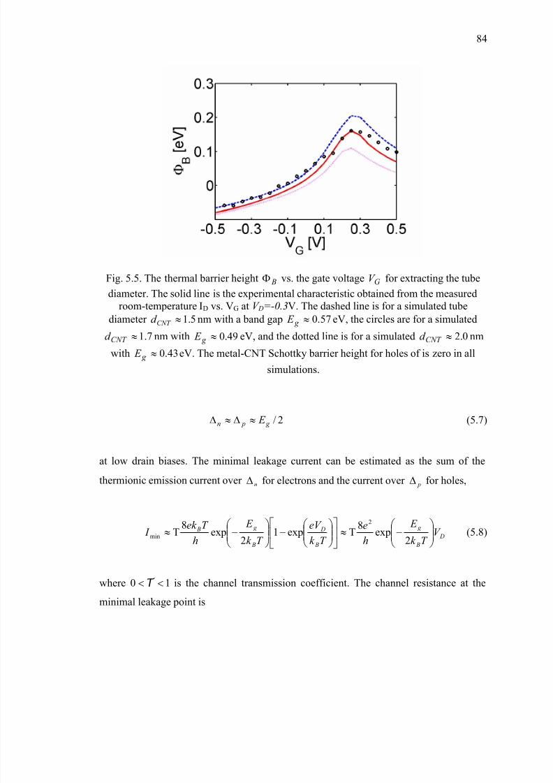
Next we extract the bandgap and the diameter of the carbon nanotube channel. Fig.
5.5 shows the experimental BΦ - VG characteristic (the circles), and the simulated BΦ -
VG curves for three different tube diameters, d CNT ~1.5nm (the dashed line), d CNT ~1.7nm
(the solid line), and d CNT ~2.0nm (the dotted line). The maximumB
Φ in the curve (which
corresponds to the minimal leakage current point in an ambipolar ID-VG curve) is
sensitive to the tube diameter. It is therefore, possible, to extract the tube diameter by
fitting the experimentally measured BΦ - VG curve near the largest BΦ point (or
equivalent, fitting the minimal leakage current in an ambipolar ID-VG curve). Fig. 5.5
indicates that the best fitting is achieved when the tube diameter d CNT ~1.7nm, which
results in a tube band gap of E g ~0.49eV. The numerical fitting techniques only needs a
room-temperature I-V and simplifies the measurement, but the analysis based on detailed
numerical simulation is time-consuming. Alternatively, the tube diameter and band gap
can also be extracted from temperature-dependent measurement using a simple analysis
as described next.
Fig. 5.6a sketches the log (ID) vs. VG characteristic for a CNTFET with a thin gate
oxide, which displays electron conduction at high gate voltages and hole conduction a
low gate voltages [9, 10]. The band gap can be extracted from the electrical
characterization of the minimal leakage point. Fig. 5.6b sketches the band diagram at the
minimal leakage point at a low VD for a CNTFET with zero barrier height for holes.
Although a high SB exists for electron transport, the SB is nearly transparent for electron
tunneling for two reasons. The first reason is that the SB for a high-performance
transistor is thin when the gate oxide is thin. (The SB thickness is approximately the same
as the gate oxide thickness [60]). The second reason is that the small carrier effective
mass in CNTs greatly facilitates quantum-mechanical tunneling [63]. The barrier that
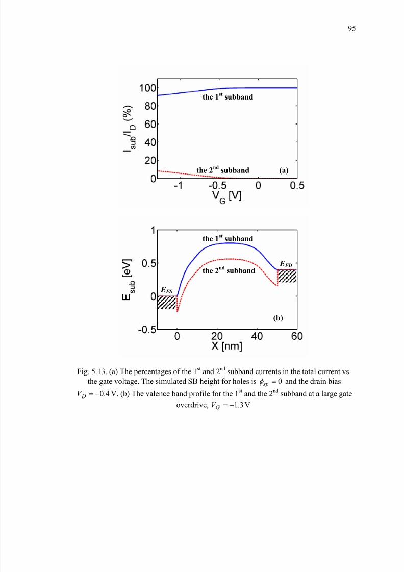
limits the electron leakage current is the thermal barrier in the CNT body, n∆ , as shownin Fig. 6b. Notice that at the minimal leakage point, the electron current is equal to the
hole current. In terms of barrier height, this requires
Fig. 5.5. The thermal barrier height BΦ vs. the gate voltage GV for extracting the tubediameter. The solid line is the experimental characteristic obtained from the measured
room-temperature ID vs. VG at V D=-0.3V. The dashed line is for a simulated tubediameter 5.1≈CNT d nm with a band gap 57.0≈g E eV, the circles are for a simulated
7.1≈CNT d nm with 49.0≈g E eV, and the dotted line is for a simulated 0.2≈CNT d nm
with 43.0≈g E eV. The metal-CNT Schottky barrier height for holes of is zero in all
simulations.
2/g pn E ≈∆≈∆ (5.7)
at low drain biases. The minimal leakage current can be estimated as the sum of the
thermionic emission current over n∆ for electrons and the current over p∆ for holes,
D
B
g
B
D
B
g B V T k
E
h
e
T k
eV
T k
E
h
T ek I
−≈
−
−≈
2exp
8Texp1
2exp
8T
2
min (5.8)
where 10 <<T is the channel transmission coefficient. The channel resistance at the
The temperature dependence of R0 is small compared to the exponential factor in eqn.
(9). The CNT band gap, therefore, can be extracted from the slope of the )ln( minR vs.
1/T plot using a temperature dependent measurement,
)ln(
1
2)ln( 0min RT k
E
R B
g
+= . (5.10)
As shown in [14], the band-gap extracted by using this temperature-dependent
measurement is 50.0≈g E eV, which is in good agreement with the value obtained by
numerically fitting ( 49.0≈g E eV).
Fig. 5.6. (a) log ID vs. VG sketch for a thin-gate-oxide CNTFET with metal contacts.
When the gate oxide is thin, the transistor shows ambipolar conduction. At the minimalleakage current (the circled point), the electron current is equal to the hole current. (b)The band diagram sketch at the minimal leakage point for a CNTFET with a thin gateoxide at a low VD. The SB height for holes is zero ( 0=bpφ ). n∆ ( p∆ ) is the thermal
barrier height for electrons (holes) in the CNT channel.
In this section, we use quantum simulations to understand what controls the transistor
performance and to suggest possible optimization to further improve transistor
performance. Fig. 5.7 plots the experimental (the circles) and the theoretical (the lines) ID
vs. VG characteristics. In the quantum simulation, the SB height 0=bpφ , the tube
diameter d CNT ~1.7nm, and the CNT channel is treated as a ballistic conductor. The
simulated subthreshold swing at V D=0.3V is S ~80mV/dec, which is larger than the
theoretical limit, 60mV/dec, but smaller than the measured value at VD = 0.3V, of
~110mV/dec. The degradation of the simulated S from the ideal value is due to the thin
bottom gate oxide, which is only ~10nm thick. The capacitance between the tube and the
bottom gate electrode is still considerable, compared to the capacitance between the tube
and the top gate. The existence of the bottom gate capacitance degrades S from the
theoretical limit value to ~80mV/dec. Using a thicker bottom gate oxide can improve the
subthreshold swing. Although the back gate parasitic capacitance is included in the
simulation, the simulated value (S~80mV/dec) is still smaller than the measured value
(S~110mV/dec), which can be due to other factors like significant interface charge states
at the HfO2 and SiO2 interface.
The possible existence of significant interface/oxide charge is also consistent with thediscrepancy between the simulated and measured threshold voltage. The threshold
voltage of a transistor is determined by the gate-channel work function difference and
interface/oxide charges [62]. Our simulation includes gate-CNT work function difference
but no oxide/interface charges. The simulated threshold voltage is found to be ~0.75V
smaller than the experimentally measured value. The mismatch of VT between
experiments and simulation after the HfO2 top gate insulator deposition can be due to
factors, such as the significant HfO2/SiO2 interface charges. The mismatch can also be
due to the uncertainty of the top and bottom gate workfunction used as the simulation
input. The oxidation of the Al top gate can change its work function from the value for
pure Al and the doping density of the bottom gate can also charge the workfunction of the
Fig. 5.7. The experimental (the dashed lines) and simulated (the solid lines) ID vs. VG characteristics at V D=-0.1, -0.2, and -0.3V. For the simulated CNTFET, the Schottky
barrier height for holes is 0=bpφ and the tube diameter 7.1≈CNT d nm. The CNT work
function 7.4=ΦCNT eV, the Al top gate work function 1.4=Φ Al eV, and the p+ doped
bottom gate work function 1.5=Φ pSi eV. No interface and oxide charges are included.
The simulated curves are translated by +0.75V along the x-axis to match theexperimental curves.
Figure 5.8 plots the experimental ID vs. VG characteristic at V G=-0.4V (circles). To
explore how close the experimental FET operates to its ballistic limit, we simulated the ID
vs. VG characteristics for a ballistic CNTFET with zero SB, 0=bpφ , and zero parasitic
source/drain resistance, 0, =DS R (the solid line). The experimental FET delivers >90%
on-current of the ballistic current of the 0=bpφ CNTFET. The performance of a zero SB
transistor can be further improved if the barrier height can be made negative [64],
because at on-state, a significant portion of carriers needs to tunnel through even though
the SB is zero. If a negative SB could be achieved, the transistor on-current will increase
and finally saturate when the SB is sufficiently negative. The on-current of a ballistic SB
transistor with a sufficiently negative barrier represents an upper-performance limit when
current is limited neither by the contact nor by scattering [64]. To explore how close the
experimental FET operates to the upper-performance limit, we also simulated the ID-VD
of a ballistic CNTFET with a sufficiently negative SB, 3.0−=bpφ V, as shown by the
dash-dot line in Fig. 8. The experimental FET delivers ~50% of the on-current of a
ballistic CNTFET with a sufficiently negative barrier height. The results indicate that the
experimental FET operates relatively close even to its upper-performance limit.
Fig. 5.8. The experimental (circles) and simulated (solid and dash-dot lines) ID vs. VD atV V G 4.0−= . The solid line is simulated for a ballistic-channel CNTFET with a zero SB
for holes ( 0=bpφ ). The dash-dot line simulated for a ballistic CNTFET with a
sufficiently negative SB height eV bp 3.0−=φ . The source/drain parasitic resistance
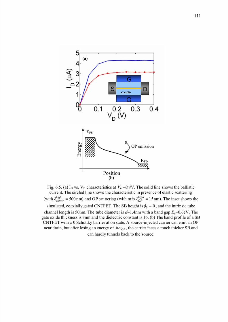
Figure 5.10 is an attempt to understand why scattering in the channel only has a small
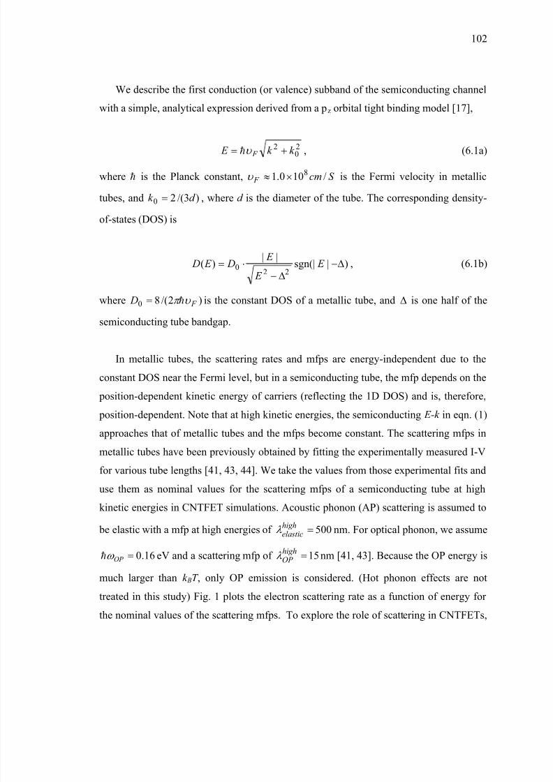
effect on the DC characteristics of the transistor. As pointed by previous studies [41, 43,
44], phonon scattering is the most important scattering mechanism in high-quality,
single-wall carbon nanotubes. Acoustic phonon scattering has a long mean free path
(~1µm) [41, 43, 44, 54, 65], therefore, it only has a small effect on the source-drain
current for Lch~50nm. Optical phonon (OP) scattering (with eV OP 16.0~ω h ) has a much
shorter mean free path (~10nm) and scatters carriers even in a short channel. Due to the
short mean free path, the carrier can emit an OP near the drain end of channel as shown
in Fig. 5.10. After OP emission, the backscattered hole encounters a much thicker and
higher SB because lose of a large OP energy eV OP 16.0~ω h . The back scattered hole
has little chance to tunnel through the SB and return back to the source. (OP absorption
can also occur if hot phonon effects are considered, but it also has a small effect on the
DC source-drain current. The treatment of hot phonon effects is beyond the scope of this
paper and will be discussed in a separate study.) Although OP emission scatters carriers
near the drain end of the channel, it only has a small effect on the DC characteristics of
the transistor. In contrast, for a ~50nm-long metallic CNT where a potential barrier does
not exist, OP emission begins to play a significant role when the applied source/drain bias
is lager than the optical phonon energy eV OP D /ω h> [43, 44].
Fig. 5.10. The valence band profile at on-state for a 0=bpφ CNTFET. Acoustic phonon
scattering has a long mean-free-path and thus a small effect on the source-drain currentfor a 50nm-channel-length CNTFET [41, 43, 44, 65]. The source injected hole can emit
an optical phonon with 16.0~OP ω h and get back scattered near drain, but the
backscattered hole encounters a much thicker and higher SB and has little chance toreturn back to the source.
Next we explore the performance improvement by the use of a high- κ top gate
insulator. Fig. 5.11a plots the ID vs. VD characteristics at VG=-0.4V for three top gate
insulators, (1) t top=8nm SiO2 as shown by the dashed line, (2) t top=8nm HfO2 used in the
experiment [14] as shown by the solid line, and (3) t top=4nm HfO2 as shown by the dotted
line. Using high-κ gate insulator with 16~κ (HfO2) instead of the SiO2 gate insulator
improves the transistor on-current by approximately a factor of 2. This result is in
contrast with a previous study [51], which indicated that little improvements could be
achieved by using high-κ gate insulator for CNTFETs. Fig. 5.11b, which plots the on-
state valence band diagram, explains the reason. At the on-state, the charge in the
nanotube channel can produce a considerable self-consistent potential which lowers the
valence band in the CNT body and increases the SB thickness at the contact. When a
high-κ gate insulator is used, the electric field produced by the charge on the tube is
effectively screened by the high- κ gate insulator, and the self-consistent potential is
smaller. Compared to the band diagram for SiO2 top gate insulator as shown in Fig. 10,
the Schottky barrier at the source contact is thinner, and the valence band in the CNT
body is more effectively lifted up by the gate voltage by applying HfO2 gate insulator.
On the other hand, a factor of 4 improvement of the gate dielectric by applying HfO2 instead of SiO2 only results in a factor of ~2 improvement of on-current for the studied
CNTFET, which is smaller than what is expected for a MOSFET-like transistor. The
major reason is that the mechanism of gate modulation for CNTFETs is different from
that for MOSFET-like transistors. For MOSFET-like transistors, the gate modulates the
channel conductance by a field in the direction normal to the channel. Increasing the gate
dielectric constant results in a proportional increase of the charge at the beginning of the
channel thereby the on-current. For CNTFETs, the gate modulates the tunneling
conductance of the metal-nanotube contact at the source using fringing field, a
modulation mechanism not as effective as that for a MOSFET-like transistor. As the
result, applying a high- κ gate insulator offers smaller on-current improvement in
Fig. 5.11. (a) The simulated ID vs. VD characteristics at V G=-0.4V for three different topgate insulators. The solid line is for the experiment with a top gate insulator thickness
t top=8nm and dielectric constant 16=κ (for HfO2). The dashed line is for SiO2 insulator with t top=8nm and 4=κ , and the dotted line is for a scaled, high-κ top gate oxide with
t top=4nm and 16=κ . The simulated SB height for holes is 0=bpφ . (b) The valence band
profile at on-state (VD=VG=-0.4V) for three top gate insulators simulated in (a).
Fig. 5.13. (a) The percentages of the 1st and 2nd subband currents in the total current vs.the gate voltage. The simulated SB height for holes is 0=spφ and the drain bias
4.0−=DV V. (b) The valence band profile for the 1st and the 2nd subband at a large gate
As the performance of CNTFETs is progressing rapidly, it is important to compare
the CNTFET performance to Si MOSFETs. A reasonable comparison requires us to: (1)
assess transistor performance at a proper power supply voltage, (2) include both the on-
state and off-state performance, and (3) fairly compare device metrics for different
channel geometries. Fig. 14 is an attempt to compare the state-of-the-art 100nm-node-
technology Si MOSFETs with the gate length LG=50nm [66] to our experimental
CNTFET also with the same LG=50nm [14]. Fig. 14a plots the transistor intrinsic delay τ
vs. ION/IOFF for both transistors, which is generated using the method described in Fig.
14b. For a specified power supply voltage V DD, an on-current and off-current is obtained
by reading the current value at the edges of the gray window in Fig. 5.14b. The transistor intrinsic delay is computed as ON DDG I V C /=τ . For the Si MOSFET, the gate
capacitance is obtained from the C-V measurement at the inversion operation region. For
the CNTFET, C G is extracted from the slope of the charge on the tube (QCNT ) vs. the top
gate voltage (V top) plot above V t for a CNT capacitor with the same gate geometry as the
experimental FET [67]. A data point on the τ vs. ION/IOFF plot is obtained. By sweeping
the gray window along the V G axis (which corresponds to adjusting the transistor
threshold voltage), an τ vs. I ON
/I OFF
curve is generated. The advantage of using τ and
I ON /I OFF for comparison is that they don’t depend on the channel geometry, and I ON /I OFF
considers both the off and on states. The results show that for an on-off ratio of 100, the
intrinsic delay of the CNTFET at V DD=0.4V is ~60% of that of the Si MOSFET at
VDD=1V, and a factor of 3-4 times smaller than Si FET delay at VDD=0.4V because the
thermal velocity in CNT is larger than that in Si, and the CNTFET operates closer to its
ballistic limit.
The performance of the analyzed experimental CNTFET can be further improved by
design optimization. As shown in Fig. 5.14a, the highest achievable on-off ratio for the
experimental CNTFET at VDD = 0.4V is only ~100, due to the ambipolar conduction of
the CNTFET. The maximum on-off current ratio can be significantly improved if a
Fig. 5.14. Comparing CNTFETs to Si MOSFETs. (a) The intrinsic transistor delay vs. theon-off ratio for a state-of-the-art Si n-type MOSFET with the gate length LG~50nm
[Let01] at the power supply voltage VDD=1V (the solid line) and V DD=0.4V (the dottedline), an experimental p-type CNTFET [Jav04a] at V DD=0.4V (the dash-dot line), and atheoretically projected CNTFET described in the text at V DD=0.4V (the dashed line). (b)
I D vs. V G characteristics of a p-type transistor, which shows the curves in (a) are
A recently demonstrated CNTFET is analyzed in detail using self-consistent quantum
simulations. The following results are obtained in this study.
(1) Pd source/drain makes a good contact to the ~1.7nm-diameter tube channel with a
Schottky barrier height 80<bφ meV. Techniques for extracting tube band gap
and diameter based on I-V measurement are proposed.
(2) Phonon scattering only has a small effect on the DC source-drain current. At
VG=-0.4V, the transistor delivers ~90% of the on-current of a ballistic CNTFET
with a zero SB, and ~50% on-current of a ballistic CNTFET with a sufficiently
negative SB.
(3) Applying high- κ gate insulator improves the CNTFET performance up to a
certain κ value. High- κ gate insulator more effectively screening the self-
consistent potential produced by the charge on the tube. Scaling down the oxide
thickness results in thinner Schottky barrier and larger on-current.
(4) Conduction through higher subbands is small compared to conduction through the
lowest subband.
(5) Further performance improvement can be achieved by using a smaller diameter tube as the channel, producing lower barrier contacts, applying thinner high-κ
gate insulator, and reducing the parasitic source/drain resistance. Other options to
significantly suppress ambipolar conduction and reduce the minimal leakage
current are to produce MOSFET-like CNTFETs, which have heavily doped CNTs
as source/drain extensions [55], or to use asymmetric source/drain design [68, 69].
(6) Under much lower power supply voltages, the delay metric of CNTFETs can be
several times smaller than that of MOSFETs operating at the same on-off ratio.
Understanding carrier transport in carbon nanotubes (CNTs) is important for both
physics and applications [5, 6]. The mean-free-paths (mfps) for elastic scattering are
known to be very long in carbon nanotubes (~1µm), but optical phonon (OP) scattering
has been shown to be important in metallic CNTs when the applied bias is larger than theoptical phonon energy (~ 160 meV) [41, 43, 44, 65]. In long, metallic CNTs, optical
phonon emission causes the current to saturate at ~25 µA, and the data can be explained
with an assumed mean free path (mfp) of ~10nm[41]. Recent experiments on metallic
nanotubes with varying lengths showed that for short, metallic nanotubes, the current can
exceed 25 µA. This data can also be explained by an OP scattering with a mfp of 10-15
nm. (Optical phonon scattering includes both intravelly scattering and intervalley
scattering caused by zone boundary phonons [43, 44]). Recently, a CNTFET with
channel length of L~50nm delivering nearly the ballistic current has been reported
[Jav04b]. This is a surprising result, because under high drain bias the channel length is
several mfps long. In this Letter, we show that even, near-ballistic DC currents can be
obtained for semiconducting CNTs, even under high source-drain bias in the presence of
significant inelastic scattering, which is different for metallic CNTs
Scattering in bulk CNTs [70, 71] and in metallic tubes [43] has been previously
explored using semiclassical Monte Carlo simulations. In this letter, we report a
simulation study of the role of phonon scattering in CNT field-effect transistors (FETs).
We show that elastic scattering has a small effect on source-drain current for a short-
channel CNTFET when the mfp is long, as it typically is for CNTs. If, however, a short
the mfps will be varied about their nominal values. (When we quote a value for the mfp
in the CNTFET simulation, we will quote the high energy mfp, which corresponds to the
constant, metallic mfp.)
Fig. 6.1. The scattering rate vs. carrier kinetic energy in the lowest subband. The elasticscattering mfp at high energies is 500nm and the OP scattering mfp at high energies is
15nm. The OP energy is 0.16eV. Only scattering within the lowest semiconducting bandis included.
Pauli blocking is an important factor that is treated using a rejection technique as
described by Lugli [74]. The carrier distribution function is updated after each time step,
so that when a scattering event occurs, the probability of whether a scattering final state is
available can be evaluated. A random number between 0 and 1 then determines whether
the scattering is permitted. To treat transistor electrostatics, Poisson’s equation is solved
self-consistently with the transport simulation. Two types of contacts are treated. For hypothetical MOSFET-like CNTFETs with doped tubes as source/drain [55] as shown in
Fig. 2a, the contacts are assumed to be ideal (without reflection). For Schottky barrier
(SB) CNTFETs [7, 8], we treat the tunneling of carriers through metal-CNT junctions as
follows. For a carrier injected to the Schottky barrier at an energy, the transmission
probability through the SB at the energy is evaluated using the WKB approximation. A
random number between 0 and 1 is then generated to determine whether the carrier
tunnels through the SB or get reflected. Such an approach has been previously developed
to treat Si SBFETs, and validated by experiments for a channel length down to ~27nm
[75].
6.3 Results
We first simulated a MOSFET-like CNTFET with doped tubes as source/drain
extensions, as shown in the inset of Fig. 2a. The doped S/D length is 15nm, and the
intrinsic, gated tube length is 20nm, which results in a total tube length of 50nm. The
solid line shows the ballistic ID vs. VD characteristics at high gate voltages (V G=0.4V). Toexplore the role of elastic scattering in CNTFETs, we first included only elastic scattering
in the CNT channel. Two different mfps were assumed: (i) a long elastic mfp,
500=highelasticλ nm, which is typical for a tube. (Note that 500=high
elasticλ nm is the mfp at
high kinetic energies, and that the thermal average mfp near the top of the barrier is
90~elasticλ nm), and (ii) a short elastic mfp, 15=highelastic
λ nm, which is the value
expected for OP scattering in CNTs, (and corresponds to a thermal average mfp of
3~elasticλ nm near the top of the barrier). The dashed line with circles in Fig. 2b shows
the I-V characteristic for case (i). For a long elastic mfp with 500=highelasticλ nm and
90~elasticλ nm, the transistor’s on-current is ~80% of the ballistic on current, and
elastic scattering has a small effect. The solid line with circles in Fig. 2b shows the I-V
characteristic for case (ii) with the short elastic mfp. The transistor on-current is
significantly degraded to only ~10% of the ballistic limit by short-mfp, elastic scattering.
To understand why elastic scattering with a short mfp has a severe effect on the
ballistic current of CNTFETs, we can compare it to the role of elastic scattering in Si
MOSFETs. As shown in Fig. 2c, for scattering near the drain end of the channel of a
MOSFET, the final k -states distribute around a circle because the channel is 2D. For most
final states, carriers don not posses enough backward velocity along the channel direction
to overcome the barrier and return to the source. For this reason, scattering near the drain
is less important than scattering near the source end of the channel [76, 77]. (Of course,
scattering near the drain causes the space charge density to build up, which has an
indirect, though potentially strong, effect on the current [46]). The result is that Si
MOSFETs with a channel length several times longer than the elastic scattering mfp (due
to, for example, surface roughness scattering) can still operate at nearly one-half of the
ballistic limit [66, 78]. For CNTFETs, however, elastic scattering anywhere in thechannel has a strong effect because the channel is one-dimensional so scattering
anywhere in the channel just reverses the direction of the carrier velocity and allows them
to return to the source over the top of the barrier as shown in Fig. 2d. The important role
of short mfp elastic scattering in CNTFETs is due to the different channel geometry.
Similar effects are expected for other nanotube/nanowire FETs, so it is important to
suppress elastic scattering, such as surface roughness scattering, in 1D-channel
nanoelectronic FETs. Compared to Si or Ge nanowire transistors, an advantage of
CNTFETs is the lack of dangling bonds and surface roughness scattering at the tube/gate
oxide interface.
Because OP scattering has a much shorter mfp than elastic scattering in CNTs, it’s
important to explore the role of OP scattering. Fig. 3a shows ID vs. VD at the ballistic
limit (the solid line), as well as the characteristics in presence of only elastic scattering
with 500=highelasticλ nm (the dashed line) and with both elastic scattering and OP scattering
with 15=highOP λ nm (the solid line with circles). It is interesting to note that although the
OP scattering mfp is much shorter than that of elastic scattering and the tube is several
times longer than the OP mfp, OP scattering has little effect on the transistor current even.
Fig. 6.3. (a) ID vs. VD at VG=0.4V for the CNTFET as shown in Fig. 6.1a. The solid lineshows the ballistic characteristics. The solid line with circles is the characteristic in
presence of both OP scattering (with mfp 15=highOP λ nm) and elastic scattering
( 500=highelasticλ nm). The dashed line with crosses shows the I-V in the presence of only
elastic scattering ( 500=high
elasticλ nm), and without OP scattering. (b) The steady-stateelectron distribution at 4.0== GD V V V. The OP scattering mfp is 15=high
OP λ nm and the
AP scattering mfp is 500=highelasticλ nm. The solid line shows the first conduction band
phonon energy in Si and GaAs,) the backscattered carrier faces a much thicker and higher
SB. Since the tunneling probability exponentially decreases with the SB thickness, the
chance for the scattered carrier to go back to source greatly reduces. OP scattering,
therefore, has little effect on the source-drain current at modest gate biases, due to the
mechanism of losing energy after scattering. Our theoretical results are consistent with a
recent experiment for an ultra-short channel CNTFET (with Lch ~50nm) [14]. Although
the experimental FET has a channel length several times longer than the OP scattering
mfp, the transistor still delivers a near ballistic DC current.
The negligible effect of OP emission in CNTFETs at modest gate biases is due to the
mechanism of losing a large OP energy ( 160~OP ω h meV) after scattering. In both
MOSFET-like CNTFETs and SB CNTFETs, losing a large energy prevents scattered
carrier to overcome (or to tunnel through) the potential barrier in the channel and to
return back to the source. OP scattering begins to play an important role when the source-
drain current is delivered over an energy range larger than OP ω h at large gate overdrives.
Compared to CNTFETs, optical phonons in Si have a much smaller energy (10-60meV),
and therefore, are expected to affect the source-drain current at much lower gate
overdrives in Si MOSFETs or Si nanowire transistors. The large OP energy in CNTs,
therefore is another advantage for delivering more current.
Only intrasubband scattering is treated in this study. At high drain voltages, carriers
in the lowest subband can gain enough kinetic energy near the drain end of the channel,
and experience inter-subanband scattering. After a carrier is scattered to a higher subband,
the potential barrier to prevent the carrier to return back to the source increases, and it
becomes more difficult for the carrier to return back to the source. Intersubband
scattering, therefore, won’t change the conclusion that phonon scattering only has a smalleffect on the DC source-drain current in the simulated CNTFETs.
Fig. 6.5. (a) ID vs. VD characteristics at V G=0.4V. The solid line shows the ballisticcurrent. The circled line shows the characteristic in presence of elastic scattering
(with 500=highelasticλ nm) and OP scattering (with mfp 15=high
OP λ nm). The inset shows the
simulated, coaxially gated CNTFET. The SB height is 0=bφ , and the intrinsic tube
channel length is 50nm. The tube diameter is d ~1.4nm with a band gap E g ~0.6eV. Thegate oxide thickness is 8nm and the dielectric constant is 16. (b) The band profile of a SBCNTFET with a 0 Schottky barrier at on state. A source-injected carrier can emit an OPnear drain, but after losing an energy of OP ω h , the carrier faces a much thicker SB and
Since the first demonstration of carbon nanotube transistor ~5-6 years ago[3, 4], the
understanding of carbon nanotube transistor is evolving and the performance of the
transistor is improving very rapidly [5, 6]. Carbon nanotube transistors with performance
greatly exceeding the state-of-the-art Si MOSFETs have been recently demonstrated [14].
The purposes of this work are to develop simulation approach and tools for carbon
nanotube electronics, and to use simulation to understand device physics and explore
device issues, which are crucial for improving device performance. It is describe in detail
as the following.
(1) Developing simulation approach for carbon nanotube transistors. Simulations
have been demonstrated useful to understand the device physics, explain
experiments, and explore issues, which still can not be explored experimentally.
The unique carrier transport properties and electrostatic geometry makes
conventional TCAD tools not applicable to carbon nanotube transistors.
Developing new simulation approach and tools, therefore, becomes necessary.
Guided and verified by experimental work through an on-going theory-
experiment collaboration, we developed self-consistent quantum simulation
approach for ballistic carbon nanotube transistors [32]. This simulator solves
Schrödinger equation with an atomistic description of the nanotube channel with
the non-equilibrium Green’s function (NEGF) formalism, in the presence of self-
consistent electrostatic field. We also investigated the role of phonon scattering in
carbon nanotubes by developing a semiclassical Monte-Carlo simulator, which iscoupled to quantum equations at metal/CNT contacts, for describing the quantum-
mechanical tunneling through the Schottky barriers. The self-consistent quantum
simulator allows us to treat the quantum-mechanical effects in the ballistic
[1] S. Iijima, "Helical Microtubules of Graphitic Carbon," Nature, vol. 354, pp. 56-58,1991.
[2] R. H. Baughman, A. A. Zakhidov, and W. A. de Heer, "Carbon nanotubes - theroute toward applications," Science, vol. 297, pp. 787-792, 2002.
[3] R. Martel, T. Schmidt, H. R. Shea, T. Hertel, and P. Avouris, "Single- and multi-wall carbon nanotube field-effect transistors," Applied Physics Letters, vol. 73, pp.2447-2449, 1998.
[4] S. J. Tans, A. R. M. Verschueren, and C. Dekker, "Room-temperature transistor based on a single carbon nanotube," Nature, vol. 393, pp. 49-52, 1998.
[5] P. Avouris, J. Appenzeller, R. Martel, and S. J. Wind, "Carbon nanotube
electronics," Proceedings of the Ieee, vol. 91, pp. 1772-1784, 2003.[6] P. L. McEuen, M. S. Fuhrer, and H. K. Park, "Single-walled carbon nanotubeelectronics," Ieee Transactions on Nanotechnology, vol. 1, pp. 78-85, 2002.
[7] J. Appenzeller, J. Knoch, V. Derycke, R. Martel, S. Wind, and P. Avouris, "Field-modulated carrier transport in carbon nanotube transistors," Physical ReviewLetters, vol. 89, pp. 126801.1-126801.4, 2002.
[8] S. Heinze, J. Tersoff, R. Martel, V. Derycke, J. Appenzeller, and P. Avouris,"Carbon nanotubes as Schottky barrier transistors," Physical Review Letters, vol.89, pp. 106801.1-106801.4, 2002.
[9] J. Guo, S. Datta, and M. Lundstrom, "A numerical study of scaling issues for Schottky-Barrier carbon nanotube transistors," Ieee Transactions on Electron
Devices, vol. 51, pp. 172-177, 2004.[10] M. Radosavljevic, S. Heinze, J. Tersoff, and P. Avouris, "Drain voltage scaling in
carbon nanotube transistors," Applied Physics Letters, vol. 83, pp. 2435-2437,2003.
[11] A. Javey, H. Kim, M. Brink, Q. Wang, A. Ural, J. Guo, P. McIntyre, P. McEuen,M. Lundstrom, and H. J. Dai, "High-kappa dielectrics for advanced carbon-nanotube transistors and logic gates," Nature Materials, vol. 1, pp. 241-246, 2002.
[12] S. J. Wind, J. Appenzeller, R. Martel, V. Derycke, and P. Avouris, "Fabricationand electrical characterization of top gate single-wall carbon nanotube field-effecttransistors," Journal of Vacuum Science & Technology B, vol. 20, pp. 2798-2801,2002.
[13] A. Javey, J. Guo, Q. Wang, M. Lundstrom, and H. J. Dai, "Ballistic carbonnanotube field-effect transistors," Nature, vol. 424, pp. 654-657, 2003.
[14] A. Javey, J. Guo, D. B. Farmer, Q. Wang, E. Yenilmez, R. G. Gordon, M.Lundstrom, and H. Dai, "Self-aligned ballistic molecular transistors and parallelnanotube arrays," Nano. Lett., in press, 2004.
[15] R. Saito, G. Dresselhaus, and M. S. Dresselhaus, Physical properties of carbon
[16] L. Yang, M. P. Anantram, J. Han, and J. P. Lu, "Band-gap change of carbonnanotubes: Effect of small uniaxial and torsional strain," Physical Review B, vol.60, pp. 13874-13878, 1999.
[17] J. W. Mintmire and C. T. White, "Universal density of states for carbonnanotubes," Physical Review Letters, vol. 81, pp. 2506-2509, 1998.
[18] Y. Cui, Z. H. Zhong, D. L. Wang, W. U. Wang, and C. M. Lieber, "Highperformance silicon nanowire field effect transistors," Nano Letters, vol. 3, pp.149-152, 2003.
[19] Y. Cui and C. M. Lieber, "Functional nanoscale electronic devices assembledusing silicon nanowire building blocks," Science, vol. 291, pp. 851-853, 2001.
[20] D. W. Wang, Q. Wang, A. Javey, R. Tu, H. J. Dai, H. Kim, P. C. McIntyre, T.Krishnamohan, and K. C. Saraswat, "Germanium nanowire field-effect transistorswith SiO2 and high-kappa HfO2 gate dielectrics," Applied Physics Letters, vol. 83,pp. 2432-2434, 2003.
[21] X. F. Duan, Y. Huang, R. Agarwal, and C. M. Lieber, "Single-nanowireelectrically driven lasers," Nature, vol. 421, pp. 241-245, 2003.
[22] F. Leonard and J. Tersoff, "Role of Fermi-level pinning in nanotube Schottkydiodes," Physical Review Letters, vol. 84, pp. 4693-4696, 2000.[23] F. Leonard and J. Tersoff, "Novel length scales in nanotube devices," Physical
Review Letters, vol. 83, pp. 5174-5177, 1999.[24] A. A. Odintsov, "Schottky barriers in carbon nanotube heterojunctions," Physical
Review Letters, vol. 85, pp. 150-153, 2000.[25] S. Ramo, J. R. Whinnery, and T. Van Duzer, Fields and Waves in Communication
Electronics, third ed. New York, NY, USA: John Wiley & Sons, 1993.[26] Z. Ren, "Ph. D. Thesis," Purdue University, West Lafayette, IN, 47907, 2001.[27] S. Luryi, "Quantum Capacitance Devices," Applied Physics Letters, vol. 52, pp.
501-503, 1988.[28] D. J. Frank, Y. Taur, and H. S. P. Wong, "Generalized scale length for two-
dimensional effects in MOSFET's," Ieee Electron Device Letters, vol. 19, pp.385-387, 1998.
[29] S. Datta, Electronic transport in mesoscopic systems. Cambridge ; New York:Cambridge University Press, 1995.
[30] R. Venugopal, Z. B. Ren, and M. S. Lundstrom, "Simulating quantum transport innanoscale MOSFETs: Ballistic hole transport, subband engineering and boundaryconditions," Ieee Transactions on Nanotechnology, vol. 2, pp. 135-143, 2003.
[31] A. Rahman, J. Guo, S. Datta, and M. S. Lundstrom, "Theory of ballisticnanotransistors," Ieee Transactions on Electron Devices, vol. 50, pp. 1853-1864,2003.
[32] J. Guo, S. Datta, M. Lundstrom, and M. P. Anantram, "Toward multi-scalesimulations of carbon nanotube transistors," the International Journal on
Multiscale Computer Engineering , vol. in press, 2004.[33] P. Damle, T. Rakshit, M. Paulsson, and S. Datta, "Current-voltage characteristics
of molecular conductors: Two versus three terminal," Ieee Transactions on
[34] S. Datta, "Nanoscale device modeling: the Green's function method,"Superlattices and Microstructures, vol. 28, pp. 253-278, 2000.
[35] J. Tersoff, "Schottky-Barrier Heights and the Continuum of Gap States," Physical
Review Letters, vol. 52, pp. 465-468, 1984.[36] J. Tersoff, "Reference Levels for Heterojunctions and Schottky Barriers,"
Physical Review Letters, vol. 56, pp. 675-675, 1986.[37] A. Svizhenko, M. P. Anantram, T. R. Govindan, B. Biegel, and R. Venugopal,"Two-dimensional quantum mechanical modeling of nanotransistors," Journal of
Applied Physics, vol. 91, pp. 2343-2354, 2002.[38] R. Lake, G. Klimeck, R. C. Bowen, and D. Jovanovic, "Single and multiband
modeling of quantum electron transport through layered semiconductor devices,"Journal of Applied Physics, vol. 81, pp. 7845-7869, 1997.
[39] C. P. Auth and J. D. Plummer, "Scaling theory for cylindrical, fully-depleted,surrounding-gate MOSFET's," Ieee Electron Device Letters, vol. 18, pp. 74-76,1997.
[40] F. Leonard and J. Tersoff, "Dielectric response of semiconducting carbon
nanotubes," Applied Physics Letters, vol. 81, pp. 4835-4837, 2002.[41] Z. Yao, C. L. Kane, and C. Dekker, "High-field electrical transport in single-wallcarbon nanotubes," Physical Review Letters, vol. 84, pp. 2941-2944, 2000.
[42] Z. Yao, C. Dekker, and P. Avouris, "Electrical transport through single-wallcarbon nanotubes," Carbon Nanotubes, vol. 80, pp. 147-171, 2001.
[43] A. Javey, J. Guo, M. Paulsson, Q. Wang, D. Mann, M. Lundstrom, and H. J. Dai,"High-field quasiballistic transport in short carbon nanotubes," Physical Review
Letters, vol. 92, pp.106804.1-106804.4, 2004.[44] J. Y. Park, S. Rosenblatt, Y. Yaish, V. Sazonova, H. Ustunel, S. Braig, T. A.
Arias, P. W. Brouwer, and P. L. McEuen, "Electron-phonon scattering in metallicsingle-walled carbon nanotubes," Nano Letters, vol. 4, pp. 517-520, 2004.
[45] M. V. Fischetti and S. E. Laux, "Monte-Carlo Analysis of Electron-Transport inSmall Semiconductor-Devices Including Band-Structure and Space-ChargeEffects," Physical Review B, vol. 38, pp. 9721-9745, 1988.
[46] R. Venugopal, M. Paulsson, S. Goasguen, S. Datta, and M. S. Lundstrom, "Asimple quantum mechanical treatment of scattering in nanoscale transistors,"Journal of Applied Physics, vol. 93, pp. 5613-5625, 2003.
[47] R. Venugopal, S. Goasguen, S. Datta, and M. S. Lundstrom, "Quantummechanical analysis of channel access geometry and series resistance in nanoscaletransistors," Journal of Applied Physics, vol. 95, pp. 292-305, 2004.
[48] A. Raychowdhury, S. Mukhopadhyay, and K. Roy, "Circuit-compatible modelingof carbon nanotube FETs in the ballistic limit of performance," presented at IEEEConference on Nanotechnology, San Francisco, CA, 2003.
[49] S. Rosenblatt, Y. Yaish, J. Park, J. Gore, V. Sazonova, and P. L. McEuen, "Highperformance electrolyte gated carbon nanotube transistors," Nano Letters, vol. 2,pp. 869-872, 2002.
[50] S. J. Wind, J. Appenzeller, R. Martel, V. Derycke, and P. Avouris, "Verticalscaling of carbon nanotube field-effect transistors using top gate electrodes (vol80, pg 3817, 2002)," Applied Physics Letters, vol. 81, pp. 1359-1359, 2002.
[66] A. Lochtefeld and D. A. Antoniadis, "On experimental determination of carrier velocity in deeply scaled NMOS: How close to the thermal limit?," IEEE Electron
Device Letters, vol. 22, pp. 95-97, 2001.[67] J. Guo, S. Goasguen, M. Lundstrom, and S. Datta, "Metal-insulator-
semiconductor electrostatics of carbon nanotubes," Applied Physics Letters, vol.
81, pp. 1486-1488, 2002.[68] S. Heinze, J. Tersoff, and P. Avouris, "Electrostatic engineering of nanotubetransistors for improved performance," Applied Physics Letters, vol. 83, pp. 5038-5040, 2003.
[69] Y. M. Lin, J. Appenzeller, and P. Avouris, "Ambipolar-to-unipolar conversion of carbon nanotube transistors by gate structure engineering," Nano Letters, vol. 4,pp. 947-950, 2004.
[70] G. Pennington and N. Goldsman, "Semiclassical transport and phonon scatteringof electrons in semiconducting carbon nanotubes," Physical Review B, vol. 68, p.045426, 2003.
[71] G. Pennington and N. Goldsman, "Monte Carlo study of electron transport in a
carbon nanotube," Ieice Transactions on Electronics, vol. E86C, pp. 372-378,2003.[72] K. Hess, Monte Carlo device simulation : full band and beyond . Boston: Kluwer
Academic, 1991.[73] G. D. Mahan, "Electron-optical phonon interaction in carbon nanotubes,"
Physical Review B, vol. 68, p. 125409, 2003.[74] C. Jacoboni and P. Lugli, The Monte Carlo method for semiconductor device
simulation. Wien ; New York: Springer-Verlag, 1989.[75] B. Winstead and U. Ravaioli, "Simulation of Schottky barrier MOSFET's with a
coupled quantum injection/Monte Carlo technique," Ieee Transactions onElectron Devices, vol. 47, pp. 1241-1246, 2000.
[76] M. Lundstrom and Z. B. Ren, "Essential physics of carrier transport in nanoscaleMOSFETs," Ieee Transactions on Electron Devices, vol. 49, pp. 133-141, 2002.
[77] M. Lundstrom, "Elementary scattering theory of the Si MOSFET," Ieee Electron
Device Letters, vol. 18, pp. 361-363, 1997.[78] F. Assad, Z. B. Ren, D. Vasileska, S. Datta, and M. Lundstrom, "On the
performance limits for Si MOSFET's: A theoretical study," Ieee Transactions on
Electron Devices, vol. 47, pp. 232-240, 2000.[79] J. Appenzeller and D. J. Frank, "Frequency dependent characterization of
transport properties in carbon nanotube transistors," Applied Physics Letters, vol.84, pp. 1771-1773, 2004.
[80] D. J. Frank and J. Appenzeller, "High-frequency response in carbon nanotubefield-effect transistors," Ieee Electron Device Letters, vol. 25, pp. 34-36, 2004.
[81] Q. F. Pengfei, O. Vermesh, M. Grecu, A. Javey, O. Wang, H. J. Dai, S. Peng, andK. J. Cho, "Toward large arrays of multiplex functionalized carbon nanotubesensors for highly sensitive and selective molecular detection," Nano Letters, vol.3, pp. 347-351, 2003.
[82] S. Peng, K. J. Cho, P. F. Qi, and H. J. Dai, "Ab initio study of CNT NO2 gassensor," Chemical Physics Letters, vol. 387, pp. 271-276, 2004.
[83] R. J. Chen, S. Bangsaruntip, K. A. Drouvalakis, N. W. S. Kam, M. Shim, Y. M.Li, W. Kim, P. J. Utz, and H. J. Dai, "Noncovalent functionalization of carbonnanotubes for highly specific electronic biosensors," Proceedings of the National
Academy of Sciences of the United States of America, vol. 100, pp. 4984-4989,2003.
[84] K. Besteman, J. O. Lee, F. G. M. Wiertz, H. A. Heering, and C. Dekker,"Enzyme-coated carbon nanotubes as single-molecule biosensors," Nano Letters,vol. 3, pp. 727-730, 2003.
[85] Y. Cui, Q. Q. Wei, H. K. Park, and C. M. Lieber, "Nanowire nanosensors for highly sensitive and selective detection of biological and chemical species,"Science, vol. 293, pp. 1289-1292, 2001.
[86] J. Hahm and C. M. Lieber, "Direct ultrasensitive electrical detection of DNA andDNA sequence variations using nanowire nanosensors," Nano Letters, vol. 4, pp.51-54, 2004.
Fig. A1. Computing the source self-energy for a zigzag nanotube. The circles representA-type carbon rings and the triangles represent B-type carbon rings. ig is the surface
Green’s function for the ith carbon ring inside the source. 1β ( 2β ) is the first (second)
kind coupling matrix between neighboring rings, as described in the text.
Note that the potential is invariant inside the source, so 21 α α = . Furthermore, 31 g g = due to the periodicity of the nanotube lattice. Using these relations, eqn. (A2) becomes
two coupled matrix equations with two unknowns, 1g and 2g . The surface Green’s
function can be numerically solved from Eqn (A2). The non-zero submatrix of the source
self-energy matrix is +=Σ 1111,1 β β g S , where the superscript denotes that it is the (1,1)
submatrix of the overall source self-energy matrix. The self-energy for the drain contact
Appendix B. The transistor Hamiltonian in mode space
The following basis transformation, which transforms the real space basis around the
nanotube to a mode space basis, is performed to the Hamiltonian matrix in the real space,
=+
++
............
...51
142
231
122
21
'
V
V
V
V
V
V
V
V
V
V
H
α β
β α β
β α β
β α β
β α
=+
+
......
...''
''
'''
'''
'
51
14'2
231
122
'21
α β
β α β
β α β
β α β
β α
(B1)
with
V V ii α α +=' ,
V V 1'1 β β += , and
V V 2'2 β β += , (B2)
where V is the transform matrix from the real space basis of a carbon atom ring to themode space basis. Our purpose is to uncouple the modes after the basis transformation,
i.e., to make the Hamiltonian matrix elements between different modes equal to zero.
This requires that after the transformation, 'iα , '
where qg 1 and qg 2 are the surface Green’s functions for the first and second node inside
the source as shown in Fig. A1, and U1 is the source potential. The recursive equations inthe mode space are number equations and can be analytically solved,
g 1q =(E −U 1)
2 + b12 − b2q
2 ± (E −U 1)2 + b1
2 − b2q2[ ]
2− 4(E −U 1)2 b1
2
2b12(E −U 1)
. (B10)
The retarded surface Green’s function for the first node inside the source, r qg 1 , is the
one with the negative imaginary part, and the source self-energy for the qth mode is