Joseph Henry Laboratories, Department of Physics, Princeton University, Princeton, NewJersey 08544, USA
C. L. Kane†
Department of Physics and Astronomy, University of Pennsylvania, Philadelphia,Pennsylvania 19104, USA
Published 8 November 2010
Topological insulators are electronic materials that have a bulk band gap like an ordinary insulator buthave protected conducting states on their edge or surface. These states are possible due to thecombination of spin-orbit interactions and time-reversal symmetry. The two-dimensional 2Dtopological insulator is a quantum spin Hall insulator, which is a close cousin of the integer quantumHall state. A three-dimensional 3D topological insulator supports novel spin-polarized 2D Diracfermions on its surface. In this Colloquium the theoretical foundation for topological insulators andsuperconductors is reviewed and recent experiments are described in which the signatures oftopological insulators have been observed. Transport experiments on HgTe/CdTe quantum wells aredescribed that demonstrate the existence of the edge states predicted for the quantum spin Hallinsulator. Experiments on Bi1−xSbx, Bi2Se3, Bi2Te3, and Sb2Te3 are then discussed that establish thesematerials as 3D topological insulators and directly probe the topology of their surface states. Exoticstates are described that can occur at the surface of a 3D topological insulator due to an inducedenergy gap. A magnetic gap leads to a novel quantum Hall state that gives rise to a topologicalmagnetoelectric effect. A superconducting energy gap leads to a state that supports Majoranafermions and may provide a new venue for realizing proposals for topological quantum computation.Prospects for observing these exotic states are also discussed, as well as other potential deviceapplications of topological insulators.
1. Bogoliubov–de Gennes theory 30502. Majorana fermion boundary states 30513. Periodic Table 3051
III. Quantum Spin Hall Insulator 3052A. Model system: Graphene 3052B. HgTe/CdTe quantum well structures 3053
IV. 3D Topological Insulators 3054A. Strong and weak topological insulators 3054B. The first 3D topological insulator: Bi1−xSbx 3055C. Second generation materials: Bi2Se3, Bi2Te3, and
Sb2Te3 3058
V. Exotic Broken Symmetry Surface Phases 3061A. Quantum Hall effect and topological
magnetoelectric effect 30611. Surface quantum Hall effect 30612. Topological magnetoelectric effect and
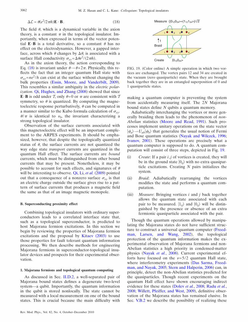
1. Majorana fermions and topologicalquantum computing 3062
2. Majorana fermions on topological insulators 3063VI. Conclusion and Outlook 3064
Acknowledgments 3064References 3065
I. INTRODUCTION
A recurring theme in condensed-matter physics hasbeen the discovery and classification of distinctivephases of matter. Often, phases can be understood usingLandau’s approach, which characterizes states in termsof underlying symmetries that are spontaneously bro-ken. Over the past 30 years, the study of the quantumHall effect has led to a different classification paradigmbased on the notion of topological order Thouless et al.,1982; Wen, 1995. The state responsible for the quantumHall effect does not break any symmetries, but it definesa topological phase in the sense that certain fundamen-tal properties such as the quantized value of the Hall
conductance and the number of gapless boundarymodes are insensitive to smooth changes in materialparameters and cannot change unless the system passesthrough a quantum phase transition.
In the past five years a new field has emerged incondensed-matter physics based on the realization thatthe spin-orbit interaction can lead to topological insulat-ing electronic phases Kane and Mele, 2005a, 2005b; Fu,Kane, and Mele, 2007; Moore and Balents, 2007; Roy,2009b and on the prediction and observation of thesephases in real materials Bernevig, Hughes, and Zhang,2006; Fu and Kane, 2007; König et al., 2007; Hsieh et al.,2008; Xia, Qian, Hsieh, Wray, et al., 2009; Zhang, Liu, etal., 2009. A topological insulator, like an ordinary insu-lator, has a bulk energy gap separating the highest occu-pied electronic band from the lowest empty band. Thesurface or edge in two dimensions of a topological in-sulator, however, necessarily has gapless states that areprotected by time-reversal symmetry. The topological in-sulator is closely related to the two-dimensional 2Dinteger quantum Hall state, which also has unique edgestates. The surface or edge states of a topological insu-lator lead to a conducting state with properties unlikeany other known one-dimensional 1D or 2D electronicsystems. In addition to their fundamental interest, thesestates are predicted to have special properties that couldbe useful for applications ranging from spintronics toquantum computation.
The concept of topological order Wen, 1995 is oftenused to characterize the intricately correlated fractionalquantum Hall states Tsui, Stormer, and Gossard, 1982,which require an inherently many-body approach to un-derstand Laughlin, 1983. However, topological consid-erations also apply to the simpler integer quantum Hallstates Thouless et al., 1982, for which an adequate de-scription can be formulated in terms of single-particlequantum mechanics. In this regard, topological insula-tors are similar to the integer quantum Hall effect. Dueto the presence of a single-particle energy gap, electron-electron interactions do not modify the state in an essen-tial way. Topological insulators can be understood withinthe framework of the band theory of solids Bloch,1929. It is remarkable that after more than 80 years,there are still treasures to be uncovered within bandtheory.
In this Colloquium, we review the theoretical and ex-perimental foundations of this rapidly developing field.We begin in Sec. II with an introduction to topologicalband theory, in which we explain the topological orderin the quantum Hall effect and in topological insulators.We also give a short introduction to topological super-conductors, which can be understood within a similarframework. A unifying feature of these states is thebulk-boundary correspondence, which relates the topo-logical structure of bulk crystal to the presence of gap-less boundary modes. Section III describes the 2D topo-logical insulator, also known as a quantum spin Hallinsulator, and discusses the discovery of this phase inHgCdTe quantum wells. Section IV is devoted to three-dimensional 3D topological insulators. We review their
experimental discovery in Bi1−xSbx, as well as more re-cent work on “second-generation” materials Bi2Se3 andBi2Te3. Section V focuses on exotic states that can occurat the surface of a topological insulator due to an in-duced energy gap. An energy gap induced by a magneticfield or proximity to a magnetic material leads to a novelquantum Hall state along with a topological magneto-electric effect. An energy gap due to proximity with asuperconductor leads to a state that supports Majoranafermions and may provide a new venue for realizing pro-posals for topological quantum computation. In Sec. VIwe conclude with a discussion of new materials, new ex-periments, and open problems.
Some aspects of this subject have been described inother reviews, including the review of the quantum spinHall effect by König et al. 2008 and surveys by Moore2010 and Qi and Zhang 2010.
II. TOPOLOGICAL BAND THEORY
A. The insulating state
The insulating state is the most basic state of matter.The simplest insulator is an atomic insulator, with elec-trons bound to atoms in closed shells. Such a material iselectrically inert because it takes a finite energy to dis-lodge an electron. Stronger interaction between atomsin a crystal leads to covalent bonding. One of the tri-umphs of quantum mechanics in the 20th century wasthe development of the band theory of solids, which pro-vides a language for describing the electronic structureof such states. This theory exploits the translational sym-metry of the crystal to classify electronic states in termsof their crystal momentum k, defined in a periodic Bril-louin zone. The Bloch states umk, defined in a singleunit cell of the crystal, are eigenstates of the BlochHamiltonian Hk. The eigenvalues Emk define energybands that collectively form the band structure. In aninsulator an energy gap separates the occupied valence-band states from the empty conduction-band states.Though the gap in an atomic insulator, such as solid ar-gon, is much larger than that of a semiconductor, there isa sense in which both belong to the same phase. One canimagine tuning the Hamiltonian so as to interpolate con-tinuously between the two without closing the energygap. Such a process defines a topological equivalencebetween different insulating states. If one adopts aslightly coarser “stable” topological classificationscheme, which equates states with different numbers oftrivial core bands, then all conventional insulators areequivalent. Indeed, such insulators are equivalent to thevacuum, which according to Dirac’s relativistic quantumtheory also has an energy gap for pair production, aconduction band electrons, and a valence band posi-trons.
Are all electronic states with an energy gap topologi-cally equivalent to the vacuum? The answer is no, andthe counterexamples are fascinating states of matter.
3046 M. Z. Hasan and C. L. Kane: Colloquium: Topological insulators
The simplest counterexample is the integer quantumHall state von Klitzing, Dorda, and Pepper, 1980;Prange and Girvin, 1987, which occurs when electronsconfined to two dimensions are placed in a strong mag-netic field. The quantization of the electrons’ circularorbits with cyclotron frequency c leads to quantizedLandau levels with energy m=cm+1/2. If N Lan-dau levels are filled and the rest are empty, then an en-ergy gap separates the occupied and empty states just asin an insulator. Unlike an insulator, though, an electricfield causes the cyclotron orbits to drift, leading to a Hallcurrent characterized by the quantized Hall conductivity,
xy = Ne2/h . 1
The quantization of xy has been measured to 1 part in109 von Klitzing, 2005. This precision is a manifestationof the topological nature of xy.
Landau levels can be viewed as a “band structure.”Since the generators of translations do not commutewith one another in a magnetic field, electronic statescannot be labeled with momentum. However, if a unitcell with area 2c /eB enclosing a flux quantum is de-fined, then lattice translations do commute, so Bloch’stheorem allows states to be labeled by 2D crystal mo-mentum k. In the absence of a periodic potential, theenergy levels are simply the k independent Landau lev-els Emk=m. In the presence of a periodic potentialwith the same lattice periodicity, the energy levels willdisperse with k. This leads to a band structure that looksidentical to that of an ordinary insulator.
1. The TKNN invariant
What is the difference between a quantum Hall statecharacterized by Eq. 1 and an ordinary insulator? Theanswer, explained by Thouless, Kohmoto, Nightingale,and den Nijs 1982 TKNN, is a matter of topology. A2D band structure consists of a mapping from the crystalmomentum k defined on a torus to the Bloch Hamil-tonian Hk. Gapped band structures can be classifiedtopologically by considering the equivalence classes ofHk that can be continuously deformed into one an-other without closing the energy gap. These classes aredistinguished by a topological invariant nZ Z denotesthe integers called the Chern invariant.
The Chern invariant is rooted in the mathematicaltheory of fiber bundles Nakahara, 1990, but it can beunderstood physically in terms of the Berry phaseBerry, 1984 associated with the Bloch wave functionsumk. Provided there are no accidental degeneracieswhen k is transported around a closed loop, umk ac-quires a well defined Berry phase given by the line inte-gral of Am= iumkum. This may be expressed as a sur-face integral of the Berry flux Fm=Am. The Cherninvariant is the total Berry flux in the Brillouin zone,
nm =1
2 d2k Fm. 2
nm is integer quantized for reasons analogous to thequantization of the Dirac magnetic monopole. The totalChern number, summed over all occupied bands, n=m=1
N nm is invariant even if there are degeneracies be-tween occupied bands, provided the gap separating oc-cupied and empty bands remains finite. TKNN showedthat xy, computed using the Kubo formula, has thesame form, so that N in Eq. 1 is identical to n. TheChern number n is a topological invariant in the sensethat it cannot change when the Hamiltonian variessmoothly. This helps to explain the robust quantizationof xy.
The meaning of Eq. 2 can be clarified by a simpleanalogy. Rather than maps from the Brillouin zone to aHilbert space, consider simpler maps from two to threedimensions, which describe surfaces. 2D surfaces can betopologically classified by their genus g, which countsthe number of holes. For instance, a sphere Fig. 1chas g=0, while a donut Fig. 1f has g=1. A theorem inmathematics due to Gauss and Bonnet Nakahara, 1990states that the integral of the Gaussian curvature over aclosed surface is a quantized topological invariant, andits value is related to g. The Chern number is an integralof a related curvature.
2. Graphene, Dirac electrons, and Haldane model
A simple example of the quantum Hall effect in aband theory is provided by a model of graphene in aperiodic magnetic field introduced by Haldane 1988.We briefly digress here to introduce graphene because itwill provide insight into the conception of the 2D quan-tum spin Hall insulator and because the physics of Diracelectrons present in graphene has important parallels atthe surface of a 3D topological insulator.
B
Insulating State
Quantum Hall State
E
k
0
E
k
EG
(a) (b) (c)
(d) (e) (f)
/a−π/a−π
0 /a−π/a−π
hωc
FIG. 1. Color online States of matter. a–c The insulatingstate. a An atomic insulator. b A simple model insulatingband structure. d–f The quantum Hall state. d The cyclo-tron motion of electrons. e The Landau levels, which may beviewed as a band structure. c and f Two surfaces whichdiffer in their genus, g. c g=0 for the sphere and f g=1 forthe donut. The Chern number n that distinguishes the twostates is a topological invariant similar to the genus.
3047M. Z. Hasan and C. L. Kane: Colloquium: Topological insulators
Graphene is a 2D form of carbon that is of currentinterest Novoselov et al., 2005; Zhang et al., 2005; Geimand Novoselov, 2007; Castro Neto et al., 2009. Whatmakes graphene interesting electronically is the fact thatthe conduction band and valence band touch each otherat two distinct points in the Brillouin zone. Near thosepoints the electronic dispersion resembles the linear dis-persion of massless relativistic particles, described by theDirac equation DiVincenzo and Mele, 1984; Semenoff,1984. The simplest description of graphene employs atwo band model for the pz orbitals on the two equivalentatoms in the unit cell of graphene’s honeycomb lattice.The Bloch Hamiltonian is then a 22 matrix,
Hk = hk · , 3
where = x ,y ,z are Pauli matrices and hk= „hxk ,hyk ,0…. The combination of inversion P andtime-reversal T symmetry requires hzk=0 because Ptakes hzk to −hz−k, while T takes hzk to +hz−k.The Dirac points occur because the two componentshk can have point zeros in two dimensions. Ingraphene they occur at two points, K and K=−K,whose locations at the Brillouin-zone corners are fixedby graphene’s rotational symmetry. For small qk−K,hq=vFq, where vF is a velocity, so Hq=vFq · hasthe form of a 2D massless Dirac Hamiltonian.
The degeneracy at the Dirac point is protected by Pand T symmetry. By breaking these symmetries the de-generacy can be lifted. For instance, P symmetry is vio-lated if the two atoms in the unit cell are inequivalent.This allows hzk to be nonzero. If hzk is small, thennear K Eq. 3 becomes a massive Dirac Hamiltonian,
Hq = vFq · + mz, 4
where m=hzK. The dispersion Eq= ±vFq2+m2
has an energy gap 2m. Note that T symmetry requiresthe Dirac point at K to have a mass m=hzK with thesame magnitude and sign, m=m. This state describes anordinary insulator.
Haldane 1988 imagined lifting the degeneracy bybreaking T symmetry with a magnetic field that is zeroon the average but has the full symmetry on the lattice.This perturbation allows nonzero hzk and introduces amass to the Dirac points. However, P symmetry requiresthe masses at K and K to have opposite signs, m=−m.Haldane showed that this gapped state is not an insula-tor but rather a quantum Hall state with xy=e2 /h.
This nonzero Hall conductivity can be understood interms of Eq. 2. For a two level Hamiltonian of theform of Eq. 3 it is well known that the Berry fluxBerry, 1984 is related to the solid angle subtended by
the unit vector hk=hk / hk, so that Eq. 2 takesthe form
n =1
4 d2kkx
h kyh · h . 5
This simply counts the number of times hk wrapsaround the unit sphere as a function of k. When the
masses m=m=0, hk is confined to the equator hz=0,with a unit and opposite winding around each of theDirac points where h=0. For small but finite m, h0 everywhere, and hK visits the north or south pole,depending on the sign of m. It follows that each Diracpoint contributes ±e2 /2h to xy. In the insulating statewith m=m the two cancel, so xy=0. In the quantumHall state they add.
It is essential that there were an even number of Diracpoints since otherwise the Hall conductivity would bequantized to a half integer. This is in fact guaranteed bythe fermion doubling theorem Nielssen and Ninomiya,1983, which states that for a T invariant system Diracpoints must come in pairs. We return to this issue in Sec.IV, where the surface of a topological insulator providesa loophole for this theorem.
3. Edge states and the bulk-boundary correspondence
A fundamental consequence of the topological classi-fication of gapped band structures is the existence ofgapless conducting states at interfaces where the topo-logical invariant changes. Such edge states are wellknown at the interface between the integer quantumHall state and vacuum Halperin, 1982. They may beunderstood in terms of the skipping motion electronsexecute as their cyclotron orbits bounce off the edgeFig. 2a. Importantly, the electronic states responsiblefor this motion are chiral in the sense that they propa-gate in one direction only along the edge. These statesare insensitive to disorder because there are no statesavailable for backscattering—a fact that underlies theperfectly quantized electronic transport in the quantumHall effect.
The existence of such “one way” edge states is deeplyrelated to the topology of the bulk quantum Hall state.Imagine an interface where a crystal slowly interpolatesas a function of distance y between a quantum Hall staten=1 and a trivial insulator n=0. Somewhere alongthe way the energy gap has to vanish because otherwiseit is impossible for the topological invariant to change.There will therefore be low energy electronic statesbound to the region where the energy gap passesthrough zero. This interplay between topology and gap-
E
k
EF
0/a−π
Conduction Band
Valence Band
Quantum HallState n=1
Insulator n=0
(a) (b)
/a−π
FIG. 2. Color online The interface between a quantum Hallstate and an insulator has chiral edge mode. a The skippingcyclotron orbits. b The electronic structure of a semi-infinitestrip described by the Haldane model. A single edge state con-nects the valence band to the conduction band.
3048 M. Z. Hasan and C. L. Kane: Colloquium: Topological insulators
less modes is ubiquitous in physics and has appeared inmany contexts. It was originally found by Jackiw andRebbi 1976 in their analysis of a 1D field theory. Simi-lar ideas were used by Su, Schrieffer, and Heeger 1979to describe soliton states in polyacetalene.
A simple theory of the chiral edge states based onJackiw and Rebbi 1976 can be developed using the twoband Dirac model 4. Consider an interface where themass m at one of the Dirac points changes sign as afunction of y. We thus let m→my, where my0gives the insulator for y0 and my0 gives the quan-tum Hall state for y0. Assume m0 is fixed. TheSchrödinger equation, obtained by replacing q by −i inEq. 4, has a simple and elegant exact solution,
qxx,y eiqxx exp−
0
y
dymydy/vF 1
1 , 6
with Eqx=vFqx. This band of states intersects theFermi energy EF with a positive group velocity dE /dqx=vF and defines a right moving chiral edge mode.
In the 1980s related ideas were applied to narrow gapsemiconductors, which can be modeled using a 3D mas-sive Dirac Hamiltonian Volkov and Pankratov, 1985;Fradkin, Dagotto, and Boyanovsky, 1986. An interfacewhere the Dirac mass changes sign is associated withgapless 2D Dirac fermion states. These share some simi-larities with the surface states of a 3D topological insu-lator, but as we shall see in Sec. IV.A there is a funda-mental difference. In a separate development, Kaplan1992 showed that in lattice quantum chromodynamicsfour-dimensional 4D chiral fermions could be simu-lated on a five-dimensional lattice by introducing a simi-lar domain wall. This provided a method for circumvent-ing the doubling theorem Nielssen and Ninomiya,1983, which prevented the simulation of chiral fermionson a 4D lattice. Quantum Hall edge states and surfacestates of a topological insulator evade similar doublingtheorems.
The chiral edge states in the quantum Hall effect canbe seen explicitly by solving the Haldane model in asemi-infinite geometry with an edge at y=0. Figure 2bshows the energy levels as a function of the momentumkx along the edge. The solid regions show the bulk con-duction and valence bands, which form continuum statesand show the energy gap near K and K. A single band,describing states bound to the edge, connects the va-lence band to the conduction band with a positive groupvelocity.
By changing the Hamiltonian near the surface the dis-persion of the edge states can be modified. For instance,Eqx could develop a kink so that the edge states inter-sect EF three times—twice with a positive group velocityand once with a negative group velocity. The difference,NR−NL, between the number of right and left movingmodes, however, cannot change and is determined bythe topological structure of the bulk states. This is sum-marized by the bulk-boundary correspondence,
NR − NL = n , 7
where n is the difference in the Chern number acrossthe interface.
C. Z2 topological insulator
Since the Hall conductivity is odd under T, the topo-logically nontrivial states described in Sec. II.B.3 canonly occur when T symmetry is broken. However, thespin-orbit interaction allows a different topological classof insulating band structures when T symmetry is unbro-ken Kane and Mele, 2005a. The key to understandingthis new topological class is to examine the role of Tsymmetry for spin 1/2 particles.
T symmetry is represented by an antiunitary operator=expiSy /K, where Sy is the spin operator and K iscomplex conjugation. For spin 1/2 electrons, has theproperty 2=−1. This leads to an important constraint,known as Kramers’ theorem, which all eigenstates of a Tinvariant Hamiltonian are at least twofold degenerate.This follows because if a nondegenerate state existedthen =c for some constant c. This would mean2= c2, which is not allowed because c2−1. In the absence of spin-orbit interactions, Kramers’degeneracy is simply the degeneracy between up anddown spins. In the presence of spin-orbit interactions,however, it has nontrivial consequences.
A T invariant Bloch Hamiltonian must satisfy
Hk−1 = H− k . 8
One can classify the equivalence classes of Hamiltonianssatisfying this constraint that can be smoothly deformedwithout closing the energy gap. The TKNN invariant isn=0, but there is an additional invariant with two pos-sible values, =0 or 1 Kane and Mele, 2005b. The factthat there are two topological classes can be understoodby appealing to the bulk-boundary correspondence.
In Fig. 3 we plot analogous to Fig. 2 the electronicstates associated with the edge of a T invariant 2D insu-lator as a function of the crystal momentum along theedge. Only half of the Brillouin zone 0kx /a isshown because T symmetry requires that the other half− /ak0 is a mirror image. As in Fig. 2, the shadedregions depict the bulk conduction and valence bands
Γa Γb
Valence Band
Conduction Band
FE
k Γa Γb
Valence Band
Conduction Band
FE
kk
(a) (b)E E
FIG. 3. Color online Electronic dispersion between twoboundary Kramers degenerate points a=0 and b= /a. In athe number of surface states crossing the Fermi energy EF iseven, whereas in b it is odd. An odd number of crossingsleads to topologically protected metallic boundary states.
3049M. Z. Hasan and C. L. Kane: Colloquium: Topological insulators
separated by an energy gap. Depending on the details ofthe Hamiltonian near the edge there may or may not bestates bound to the edge inside the gap. If they arepresent, however, then Kramers’ theorem requires theyare twofold degenerate at the T invariant momenta kx=0 and /a which is the same as − /a. Away fromthese special points, labeled a,b in Fig. 3, a spin-orbitinteraction will split the degeneracy. There are two waysthe states at kx=0 and /a can connect. In Fig. 3a theyconnect pairwise. In this case the edge states can beeliminated by pushing all of the bound states out of thegap. Between kx=0 and /a, the bands intersect EF aneven number of times. In contrast, in Fig. 3b the edgestates cannot be eliminated. The bands intersect EF anodd number of times.
Which of these alternatives occurred depend on thetopological class of the bulk band structure? Since eachband intersecting EF at kx has a Kramers partner at −kx,the bulk-boundary correspondence relates the numberNK of Kramers pairs of edge modes intersecting EF tothe change in the Z2 invariants across the interface,
NK = mod 2. 9
We conclude that a 2D topological insulator has topo-logically protected edge states. These form a unique 1Dconductor, whose properties will be discussed in Sec. III.The above considerations can be generalized to 3D to-pological insulators, discussed in Sec. IV, which haveprotected surface states.
There are several mathematical formulations of the Z2invariant Kane and Mele, 2005b; Fu and Kane, 2006,2007; Fukui and Hatsugai, 2007; Moore and Balents,2007; Fukui, Fujiwara, and Hatsugai, 2008; Qi, Hughes,and Zhang, 2008; Roy, 2009a; Wang, Qi, and Zhang,2010. One approach Fu and Kane, 2006 is to define aunitary matrix wmnk= umkun−k built from theoccupied Bloch functions umk. Since is antiunitaryand 2=−1, wTk=−w−k. There are four specialpoints a in the bulk 2D Brillouin zone where k and −kcoincide, so wa is antisymmetric. The determinant ofan antisymmetric matrix is the square of its Pfaffian,which allows us to define a=Pfwa /Detwa= ±1. Provided umk is chosen continuously through-out the Brillouin zone which is always possible, thebranch of the square root can be specified globally, andthe Z2 invariant is
− 1 = a=1
4
a. 10
This formulation can be generalized to 3D topologicalinsulators and involves the eight special points in the 3DBrillouin zone.
The calculation of is simpler if the crystal has extrasymmetry. For instance, if the 2D system conserves theperpendicular spin Sz, then the up and down spins haveindependent Chern integers n↑, n↓. T symmetry requires
n↑+n↓=0, but the difference n= n↑−n↓ /2 defines aquantized spin Hall conductivity Sheng et al., 2006. TheZ2 invariant is then simply
= n mod 2. 11
While n↑, n↓ lose their meaning when Sz nonconservingterms which are inevitably present are added, retainsits identity.
If the crystal has inversion symmetry, there is anothershortcut to computing Fu and Kane, 2007. At thespecial points a the Bloch states uma are also parityeigenstates with eigenvalue ma= ±1. The Z2 invari-ant then simply follows from Eq. 10 with
a = m
ma , 12
where the product is over the Kramers pairs of occupiedbands. This has proven useful for identifying topologicalinsulators from band-structure calculations Fu andKane, 2007; Teo, Fu, and Kane, 2008; Guo and Franz,2009; Zhang, Liu, et al., 2009; Pesin and Balents, 2010.
D. Topological superconductor, Majorana fermions
Considerations of topological band theory can also beused to topologically classify superconductors. This is asubject that has seen fascinating recent theoretical de-velopments Roy, 2008; Schnyder et al., 2008; Kitaev,2009; Qi, Hughes, et al., 2009. We give an introductionthat focuses on the simplest model superconductors. Themore general case will be touched on at the end. Thissection will provide the conceptual basis for topologicalsuperconductors and explain the emergence of Majo-rana fermions in superconducting systems. It will alsoprovide background for Sec. V.B, where we discuss Ma-jorana states in superconductor-topological insulatorstructures along with possible applications to topologicalquantum computing.
1. Bogoliubov–de Gennes theory
In the BCS mean-field theory of a superconductor theHamiltonian for a system of spinless electrons may bewritten in the form de Gennes, 1966,
H − N =12
kck
†c−kHBdGk ck
c−k† , 13
where ck† is an electron creation operator and HBdG is a
22 block matrix, which in Nambu’s notation may bewritten in terms of Pauli matrices as
HBdGk = H0k − z + 1kx + 2ky. 14
Here, H0k is the Bloch Hamiltonian in the absence ofsuperconductivity and = 1+ i 2 is the BCS mean-fieldpairing potential, which for spinless particles must haveodd parity, −k=− k. For a uniform system the ex-citation spectrum of a superconductor is given by theeigenvalues of HBdG, which exhibit a superconductingenergy gap. More generally, for spatially dependent H0
3050 M. Z. Hasan and C. L. Kane: Colloquium: Topological insulators
and the Schrödinger equation associated with HBdG isknown as the Bogoliubov–de Gennes BdG equation.
Since Eq. 13 has c and c† on both sides there is aninherent redundancy built into the BdG Hamiltonian.For =0, HBdG includes two copies of H0 with oppositesign. More generally, HBdG has an intrinsic particle-holesymmetry expressed by
HBdGk−1 = − HBdG− k , 15
where the particle-hole operator =xK satisfies 2
=+1. Equation 15 follows from H0−k=H0k andthe odd parity of the real k. It follows that everyeigenstate of HBdG with energy E has a partner at −E.These two states are redundant because the Bogoliubovquasiparticle operators associated with them satisfy E
†
=−E. Thus, creating a quasiparticle in state E has thesame effect as removing one from state −E.
The particle-hole symmetry constraint 15 has a simi-lar structure to the time-reversal constraint in Eq. 8, soit is natural to consider the classes of BdG Hamiltoniansthat can be continuously deformed into one anotherwithout closing the energy gap. In the simplest case,spinless fermions, the classification can be shown to beZ2 in one dimension and Z in two dimensions. As in Sec.II.C, this can be most easily understood by appealing tothe bulk-boundary correspondence.
2. Majorana fermion boundary states
At the end of a 1D superconductor Kitaev, 2000there may or may not be discrete states within the en-ergy gap that are bound to the end Figs. 4a–4c. Ifthey are present, then every state at +E has a partner at−E. Such finite-energy pairs are not topologically pro-tected because they can simply be pushed out of theenergy gap. However, a single unpaired bound state atE=0 is protected because it cannot move away from E=0. The presence or absence of such a zero mode isdetermined by the Z2 topological class of the bulk 1Dsuperconductor.
The Bogoliubov quasiparticle states associated withthe zero modes are fascinating objects Kitaev, 2000;
Read and Green, 2000; Ivanov, 2001; Stern, von Oppen,and Mariani, 2004; Nayak et al., 2008. Due to theparticle-hole redundancy the quasiparticle operators sat-isfy 0=0
†. Thus, a quasiparticle is its own antiparticle—the defining feature of a Majorana fermion. A Majoranafermion is essentially half of an ordinary Dirac fermion.Due to the particle-hole redundancy, a single fermionicstate is associated with each pair of ±E energy levels.The presence or absence of a fermion in this state de-fines a two-level system with energy splitting E. Majo-rana zero modes must always come in pairs for in-stance, a 1D superconductor has two ends, and a wellseparated pair defines a degenerate two-level system,whose quantum state is stored nonlocally. This has pro-found implications, which we return to in Sec. V.B whendiscussing the proposal of Kitaev 2003 to use theseproperties for quantum information processing.
In two dimensions the integer classification Z gives thenumber of chiral Majorana edge modes Figs. 4d and4e, which resemble chiral modes in the quantum Halleffect but for the particle-hole redundancy. A spinlesssuperconductor with px+ ipy symmetry is the simplestmodel 2D topological superconductor. Such supercon-ductors will also exhibit Majorana bound states at thecore of vortices Caroli, de Gennes, and Matricon, 1964;Volovik, 1999; Read and Green, 2000. This may be un-derstood by considering the vortex to be a hole in thesuperconductor circled by an edge mode Fig. 4d.When the flux in the hole is h /2e the edge modes arequantized such that one state is exactly at E=0.
Majorana fermions have been studied in particle phys-ics for decades but have not been definitively observedMajorana, 1937; Wilczek, 2009. A neutrino might be aMajorana fermion. Efforts to observe certain leptonnumber violating neutrinoless double decay processesmay resolve that issue Avignone, Elliott, and Engel,2008. In condensed-matter physics, Majorana fermionscan arise due to a paired condensate that allows a pair offermionic quasiparticles to “disappear” into the conden-sate. They have been predicted in a number of physicalsystems related to the spinless px+ ipy superconductor,including the Moore-Read state of the =5/2 quantumHall effect Moore and Read, 1991; Greiter, Wen, andWilczek, 1992; Read and Green, 2000, Sr2RuO4 DasSarma, Nayak, and Tewari, 2006, cold fermionic atomsnear a Feshbach resonance Gurarie, Radzihovsky, andAndreev, 2005; Tewari et al., 2007, and 2D structuresthat combine superconductivity, magnetism, and strongspin-orbit coupling Lee, 2009; Sato and Fujimoto, 2009;Sau et al., 2010. In Sec. V.B we discuss the prospect forcreating Majorana fermion states at interfaces betweentopological insulators and ordinary superconductors Fuand Kane, 2008.
3. Periodic Table
Topological insulators and superconductors fit to-gether into a rich and elegant mathematical structurethat generalizes the notions of topological band theorydescribed above Schnyder et al., 2008; Kitaev, 2009;
k
0 0
0
∆
−∆
∆
−∆
0
Φ
(a)
(b) (c)
(d)
(e)
1D T - SC 2D T - SC
ΓE
Γ−E = Γ E†
Γ0 = Γ 0†
Γ−E=Γ E
†ΓE
FIG. 4. Color online Boundary states for a topological super-conductor TSC. a A 1D superconductor with bound statesat its ends. The end state spectrum for b an ordinary 1Dsuperconductor and c a 1D topological superconductor. d Atopological 2D superconductor with e a chiral Majorana edgemode. c A vortex with flux =h /2e is associated with a zeromode.
3051M. Z. Hasan and C. L. Kane: Colloquium: Topological insulators
Schnyder et al., 2009; Ryu et al., 2010. The classes ofequivalent Hamiltonians are determined by specifyingthe symmetry class and the dimensionality. The symme-try class depends on the presence or absence of T sym-metry 8 with 2= ±1 and/or particle-hole symmetry15 with 2= ±1. There are ten distinct classes, whichare closely related to the classification of random matri-ces of Altland and Zirnbauer 1997. The topologicalclassifications, given by Z, Z2, or 0, show a regular pat-tern as a function of symmetry class and dimensionalityand can be arranged into the Periodic Table of topologi-cal insulators and superconductors shown in Table I.
The quantum Hall state class A, no symmetry; d=2,the Z2 topological insulators class AII, 2=−1; d=2,3,and the Z2 and Z topological superconductors class D,2=1; d=1,2 described above are entries in the Peri-odic Table. There are also other nontrivial entries de-scribing different topological superconducting and su-perfluid phases. Each nontrivial phase is predicted viathe bulk-boundary correspondence to have gaplessboundary states. One notable example is superfluid3HeB Volovik, 2003; Roy, 2008; Schnyder et al., 2008;Nagato, Higashitani, and Nagai, 2009; Qi, Hughes, et al.,2009; Volovik, 2009, in class DIII, 2=−1, 2=+1; d=3 which has a Z classification along with gapless 2DMajorana fermion modes on its surface. A generaliza-tion of the quantum Hall state introduced by Zhang andHu 2001 corresponds to the d=4 entry in class A orAII. There are also other entries in physical dimensionsthat have yet to be filled by realistic systems. The searchis on to discover such phases.
III. QUANTUM SPIN HALL INSULATOR
The 2D topological insulator is known as a quantumspin Hall insulator. This state was originally theorized to
exist in graphene Kane and Mele, 2005a and in 2Dsemiconductor systems with a uniform strain gradientBernevig and Zhang, 2006. It was subsequently pre-dicted to exist Bernevig, Hughes, and Zhang, 2006 andwas then observed König et al., 2007 in HgCdTe quan-tum well structures. In Sec. III.A we introduce the phys-ics of this state in the model graphene system and de-scribe its novel edge states. Section III.B reviews theexperiments, which have also been the subject of thereview article by König et al. 2008.
A. Model system: Graphene
In Sec. II.B.2 we argued that the degeneracy at theDirac point in graphene is protected by inversion and Tsymmetry. That argument ignored the spin of the elec-trons. The spin-orbit interaction allows a new mass termin Eq. 3 with respect to all of graphene’s symmetries.In the simplest picture, the intrinsic spin-orbit interac-tion commutes with the electron spin Sz, so the Hamil-tonian decouples into two independent Hamiltonians forthe up and down spins. The resulting theory is simplytwo copies of the model of Haldane 1988 with oppositesigns of the Hall conductivity for up and down spins.This does not violate T symmetry because time reversalflips both the spin and xy. In an applied electric field,the up and down spins have Hall currents that flow inopposite directions. The Hall conductivity is thus zero,but there is a quantized spin Hall conductivity, definedby Jx
↑−Jx↓=xy
s Ey with xys =e /2—a quantum spin Hall
effect. Related ideas were mentioned in earlier work onthe planar state of 3He films Volovik and Yakovenko,1989. Since it is two copies of a quantum Hall state, thequantum spin Hall state must have gapless edge statesFig. 5.
TABLE I. Periodic table of topological insulators and superconductors. The ten symmetry classes are labeled using the notationof Altland and Zirnbauer 1997 AZ and are specified by presence or absence of T symmetry , particle-hole symmetry , andchiral symmetry =. ±1 and 0 denote the presence and absence of symmetry, with ±1 specifying the value of 2 and 2. Asa function of symmetry and space dimensionality d, the topological classifications Z, Z2, and 0 show a regular pattern that repeatswhen d→d+8.
Symmetry d
AZ 1 2 3 4 5 6 7 8
A 0 0 0 0 Z 0 Z 0 Z 0 ZAIII 0 0 1 Z 0 Z 0 Z 0 Z 0
AI 1 0 0 0 0 0 Z 0 Z2 Z2 ZBDI 1 1 1 Z 0 0 0 Z 0 Z2 Z2
D 0 1 0 Z2 Z 0 0 0 Z 0 Z2
DIII −1 1 1 Z2 Z2 Z 0 0 0 Z 0AII −1 0 0 0 Z2 Z2 Z 0 0 0 ZCII −1 −1 1 Z 0 Z2 Z2 Z 0 0 0C 0 −1 0 0 Z 0 Z2 Z2 Z 0 0CI 1 −1 1 0 0 Z 0 Z2 Z2 Z 0
3052 M. Z. Hasan and C. L. Kane: Colloquium: Topological insulators
The above discussion was predicated on the conserva-tion of spin Sz. This is not a fundamental symmetry,though, and spin nonconserving processes—present inany real system—invalidate the meaning of xy
s . Thisbrings into question theories that relied on spin conser-vation to predict an integer quantized xy
s Volovik andYakovenko, 1989; Bernevig and Zhang, 2006; Qi, Wu,and Zhang, 2006, as well as the influential theory of thenonquantized spin Hall insulator Murakami, Nagaosa,and Zhang, 2004. Kane and Mele 2005a showed thatdue to T symmetry the edge states in the quantum spinHall insulator are robust even when spin conservation isviolated because their crossing at k=0 is protected bythe Kramers degeneracy discussed in Sec. II.C. This es-tablished the quantum spin Hall insulator as a topologi-cal phase.
The quantum spin Hall edge states have the important“spin filtered” property that the up spins propagate inone direction, while the down spins propagate in theother. Such edge states were later termed “helical” Wu,Bernevig, and Zhang, 2006, in analogy with the corre-lation between spin and momentum of a particle knownas helicity. They form a unique 1D conductor that isessentially half of an ordinary 1D conductor. Ordinaryconductors, which have up and down spins propagatingin both directions, are fragile because the electronicstates are susceptible to Anderson localization in thepresence of weak disorder Anderson, 1958; Lee andRamakrishnan, 1985. By contrast, the quantum spinHall edge states cannot be localized even for strong dis-order. To see this, imagine an edge that is disordered ina finite region and perfectly clean outside that region.The exact eigenstates can be determined by solving thescattering problem relating incoming waves to those re-flected from and transmitted through the disordered re-gion. Kane and Mele 2005a showed that the reflectionamplitude is odd under T—roughly because it involvesflipping the spin. It follows that unless T symmetry isbroken, an incident electron is transmitted perfectlyacross the disordered region. Thus, eigenstates at anyenergy are extended, and at temperature T=0 the edgestate transport is ballistic. For T0 inelastic back-scattering processes are allowed, which will, in general,lead to a finite conductivity.
The edge states are similarly protected from the ef-fects of weak electron interactions, though for stronginteractions the Luttinger liquid effects lead to a mag-netic instability Wu, Bernevig, and Zhang, 2006; Xu andMoore, 2006. This strong interacting phase is interestingbecause it will exhibit charge e /2 quasiparticles similarto solitons in the model of Su, Schrieffer, and Heeger1979. For sufficiently strong interactions similar frac-tionalization could be observed by measuring shot noisein the presence of magnetic impurities Maciejko et al.,2009 or at a quantum point contact Teo and Kane,2009.
B. HgTe ÕCdTe quantum well structures
Graphene is made out of carbon—a light elementwith a weak spin-orbit interaction. Though there is dis-agreement on its absolute magnitude Huertas-Hernando, Guinea, and Brataas, 2006; Min et al., 2006;Boettger and Trickey, 2007; Yao et al., 2007; Gmitra etal., 2009, the energy gap in graphene is likely to besmall. Clearly, a better place to look for this physicswould be in materials with strong spin-orbit interactions,made from heavy elements near the bottom of the Peri-odic Table. To this end, Bernevig, Hughes, and Zhang2006 BHZ had the idea to consider quantum wellstructures of HgCdTe. This paved the way to the experi-mental discovery of the quantum spin Hall insulatorphase.
Hg1−xCdxTe is a family of semiconductors with strongspin-orbit interactions Dornhaus and Nimtz, 1983;CdTe has a band structure similar to other semiconduc-tors. The conduction-band-edge states have an s-likesymmetry, while the valence-band-edge states have ap-like symmetry. In HgTe, the p levels rise above the slevels, leading to an inverted band structure. BHZ con-sidered a quantum well structure where HgTe is sand-wiched between layers of CdTe. When the thickness ofthe HgTe layer is ddc=6.3 nm the 2D electronic statesbound to the quantum well have the normal band order.For ddc, however, the 2D bands invert. BHZ showedthat the inversion of the bands as a function of increas-ing d signals a quantum phase transition between thetrivial insulator and the quantum spin Hall insulator.This can be understood simply in the approximation thatthe system has inversion symmetry. In this case, since thes and p states have opposite parity the bands will crosseach other at dc without an avoided crossing. Thus, theenergy gap at d=dc vanishes. From Eq. 12, the changein the parity of the valence-band-edge state signals aphase transition in which the Z2 invariant changes.
Within a year of the theoretical proposal theWürzburg group, led by Laurens Molenkamp, made thedevices and performed transport experiments thatshowed the first signature of the quantum spin Hall in-sulator. König et al. 2007 measured the electrical con-ductance due to the edge states. The low-temperatureballistic edge state transport can be understood within asimple Landauer-Büttiker Büttiker, 1988 framework in
E
EF
Conduction Band
Valence Band
Quantum spinHall insulator ν=1
ConventionalInsulator
ν=0
(a) (b)
k0/a−π /a−π
FIG. 5. Color online Edge states in the quantum spin Hallinsulator QSHI. a The interface between a QSHI and anordinary insulator. b The edge state dispersion in thegraphene model in which up and down spins propagate in op-posite directions.
3053M. Z. Hasan and C. L. Kane: Colloquium: Topological insulators
which the edge states are populated according to thechemical potential of the lead that they emanate from.This leads to a quantized conductance e2 /h associatedwith each set of edge states. Figure 6d shows the resis-tance measurements for a series of samples as a functionof a gate voltage which tunes the Fermi energy throughthe bulk energy gap. Sample I is a narrow quantum wellthat has a large resistance in the gap. Samples II–IV arewider wells in the inverted regime. Samples III and IVexhibit a conductance 2e2 /h associated with the top andbottom edges. Samples III and IV have the same lengthL=1 m but different widths w=0.5 and 1 m, indicat-ing that transport is at the edge. Sample II L=20 mshowed finite temperature scattering effects. These ex-periments convincingly demonstrate the existence of theedge states of the quantum spin Hall insulator. Subse-quent experiments have established the inherently non-local electronic transport in the edge states Roth et al.,2009.
IV. 3D TOPOLOGICAL INSULATORS
In the summer of 2006 three theoretical groups inde-pendently discovered that the topological characteriza-tion of the quantum spin Hall insulator state has a natu-ral generalization in three dimensions Fu, Kane, andMele, 2007; Moore and Balents, 2007; Roy, 2009b.Moore and Balents 2007 coined the term “topologicalinsulator” to describe this electronic phase. Fu, Kane,and Mele 2007 established the connection between thebulk topological order and the presence of unique con-
ducting surface states. Soon after, this phase was pre-dicted in several real materials Fu and Kane, 2007, in-cluding Bi1−xSbx as well as strained HgTe and -Sn. In2008, Hsieh et al. 2008 reported the experimental dis-covery of the first 3D topological insulator in Bi1−xSbx.In 2009 second-generation topological insulators, includ-ing Bi2Se3, which has numerous desirable properties,were identified experimentally Xia, Qian, Hsieh, Wray,et al., 2009 and theoretically Xia, Qian, Hsieh, Wray, etal., 2009; Zhang, Liu, et al., 2009. In this section wereview these developments.
A. Strong and weak topological insulators
A 3D topological insulator is characterized by four Z2topological invariants 0 ;123 Fu, Kane, and Mele,2007; Moore and Balents, 2007; Roy, 2009b. They canbe most easily understood by appealing to the bulk-boundary correspondence, discussed in Sec. II.C. Thesurface states of a 3D crystal can be labeled with a 2Dcrystal momentum. There are four T invariant points1,2,3,4 in the surface Brillouin zone, where surfacestates, if present, must be Kramers degenerate Figs. 7aand 7b. Away from these special points, the spin-orbitinteraction will lift the degeneracy. These Kramers de-generate points therefore form 2D Dirac points in thesurface band structure Fig. 7c. The interesting ques-tion is how the Dirac points at the different T invariantpoints connect to each other. Between any pair a andb, the surface-state structure will resemble either Fig.3a or 3b. This determines whether the surface Fermisurface intersects a line joining a to b an even or anodd number of times. If it is odd, then the surface statesare topologically protected. Which of these two alterna-tives occurred is determined by the four bulk Z2 invari-ants.
The simplest nontrivial 3D topological insulators maybe constructed by stacking layers of the 2D quantumspin Hall insulator. This is analogous to a similar con-struction for 3D integer quantum Hall states Kohmoto,Halperin, and Wu, 1992. The helical edge states of thelayers then become anisotropic surface states. A pos-sible surface Fermi surface for weakly coupled layersstacked along the y direction is shown in Fig. 7a. In thisfigure a single surface band intersects the Fermi energybetween 1 and 2 and between 3 and 4, leading to thenontrivial connectivity in Fig. 3b. This layered state isreferred to as a weak topological insulator and has 0
G = .3 e2/h
G = 2 e2/h
s p
p sd
E6.3 nm
dCdTeHgTe
CdTe
eV
V 0
E
k
Normal Inverted
QSHI
(a) (b)
(c)
(d)
w
LR
14,2
3(Ω
)
Vg-Vthr (V)
FIG. 6. Color online Experiments on HgTe/CdTe quantumwells. a Quantum well structure. b As a function of layerthickness d the 2D quantum well states cross at a band inver-sion transition. The inverted state is the QSHI, which has he-lical edge states c that have a nonequilibrium population de-termined by the leads. d Experimental two terminalconductance as a function of a gate voltage that tunes EFthrough the bulk gap. Sample I, with ddc, shows insulatingbehavior, while samples III and IV show quantized transportassociated with edge states. Adapted from König et al., 2007.
(a) (b) (c)
EF
Ekxkx
kyky
Γ4Γ3
Γ1 Γ2
Γ4Γ3
Γ1 Γ2
FIG. 7. Color online Fermi circles in the surface Brillouinzone for a a weak topological insulator and b a strong to-pological insulator. c In the simplest strong topological insu-lator the Fermi circle encloses a single Dirac point.
3054 M. Z. Hasan and C. L. Kane: Colloquium: Topological insulators
=0. The indices 123 can be interpreted as Miller in-dices describing the orientation of the layers. Unlike the2D helical edge states of a single layer, T symmetry doesnot protect these surface states. Though the surfacestates must be present for a clean surface, they can belocalized in the presence of disorder. Interestingly, how-ever, a line dislocation in a weak topological insulator isassociated with protected 1D helical edge states Ran,Zhang, and Vishwanath, 2009.
0=1 identifies a distinct phase, called a strong topo-logical insulator, which cannot be interpreted as a de-scendent of the 2D quantum spin Hall insulator. 0 de-termines whether an even or an odd number of Kramerspoints is enclosed by the surface Fermi circle. In a strongtopological insulator the surface Fermi circle encloses anodd number of Kramers degenerate Dirac points. Thesimplest case, with a single Dirac point Figs. 7b and7c, can be described by the Hamiltonian
Hsurface = − ivF · , 16
where characterizes the spin. For a surface with amirror plane, symmetry requires S z .
The surface electronic structure of a topological insu-lator is similar to graphene, except rather than havingfour Dirac points 2 valley2 spin there is just a singleDirac point. This appears to violate the fermion dou-bling theorem Nielssen and Ninomiya, 1983 discussedin Sec. II.B.2. The resolution is that the partner Diracpoints reside on opposite surfaces.
The surface states of a strong topological insulatorform a unique 2D topological metal Fu and Kane, 2007;Fu, Kane, and Mele, 2007 that is essentially half an or-dinary metal. Unlike an ordinary metal, which has upand down spins at every point on the Fermi surface, thesurface states are not spin degenerate. Since T symmetryrequires that states at momenta k and −k have oppositespin, the spin must rotate with k around the Fermi sur-face, as shown in Fig. 7b. This leads to a nontrivialBerry phase acquired by an electron going around theFermi circle. T symmetry requires that this phase be 0 or. When an electron circles a Dirac point, its spin ro-tates by 2, which leads to a Berry phase.
The Berry phase has important consequences for thebehavior in a magnetic field to be discussed in Sec. V.Aand for the effects of disorder. In particular, in an ordi-nary 2D electron gas the electrical conductivity de-creases with decreasing temperature, reflecting the ten-dency toward the Anderson localization in the presenceof disorder Lee and Ramakrishnan, 1985. The Berryphase changes the sign of the weak localization correc-tion to the conductivity leading to weak antilocalizationSuzuura and Ando, 2002. In fact, the electrons at thesurface of a strong topological insulator cannot be local-ized even for strong disorder as long as the bulk energygap remains intact Nomura, Koshino, and Ryu, 2007.In this regard, the situation is similar to the edge statesof the quantum spin Hall insulator discussed in Sec.III.A; however, the electron motion on the surface isdiffusive rather than ballistic.
The Dirac surface states Eq. 16 can be understoodin a 3D Dirac theory Qi, Hughes, and Zhang, 2008where the Dirac mass changes sign at the surface, analo-gous to Eq. 6. Such domain-wall states were first dis-cussed for Pb1−xSnxTe Volkov and Pankratov, 1985;Fradkin, Dagotto, and Boyanovsky, 1986, which exhib-its a band inversion as a function of x. An appropriateinterface where x changes was predicted to have 2D gap-less states. There is an important difference betweenthese interface states and the surface states of a topo-logical insulator, though, because the band inversion inPb1−xSnxTe occurs at four equivalent valleys. Since fouris even, PbTe and SnTe are both trivial insulators. Theinterface states are not topologically protected from dis-order in the sense discussed above. However, if the val-leys can be split by applying uniaxial stress, then thetopological insulator can occur in the vicinity of theband inversion transition Fu and Kane, 2007. Relatedideas were also applied to interfaces between HgTe andCdTe Cade, 1985; Chang et al., 1985; Lin-Liu and Sham,1985; Pankratov, Pakhomov, and Volkov, 1987. In thiscase, the band inversion occurs in a single valley, butsince HgTe is a zero gap semiconductor, the surfacestates are not protected. Nonetheless, if the cubic sym-metry of the bulk HgTe can be lifted by applyinguniaxial stress, a gap can be introduced in HgTe, so theHgTe-CdTe interface will have topologically protectedstates Fu and Kane, 2007.
B. The first 3D topological insulator: Bi1−xSbx
The first 3D topological insulator to be identified ex-perimentally was the semiconducting alloy Bi1−xSbx,whose unusual surface bands were mapped in an angle-resolved photoemission spectroscopy ARPES experi-ment by a Princeton University group led by HasanHsieh et al., 2008.
Bismuth antimony alloys have long been studied fortheir thermoelectric properties Lenoir et al., 1996. Purebismuth is a semimetal with strong spin-orbit interac-tions. Its band structure, shown schematically in Fig.8a, features conduction and valence bands that over-lap, leading to pockets of holes near the T point in theBrillouin zone and pockets of electrons near the threeequivalent L points. The valence and conduction bandsat the L point, derived from antisymmetric La andsymmetric Ls orbitals, have a small energy gap . The
(a) Pure Bismuth (x=0) (b) Bi1-xSbx, 0.07<x<0.22 (c) Pure Antimony (x=1)
T L T L T L
LaLa La
LsLs
Ls
E E
k k k
EFEF
FIG. 8. Color online Schematic representation of the bandstructure of Bi1−xSbx, which evolves from semimetallic behav-ior for x0.07 to semiconducting behavior for 0.07x0.22and back to semimetallic behavior for x0.18. The conductionand valence bands Ls,a invert at x0.04.
3055M. Z. Hasan and C. L. Kane: Colloquium: Topological insulators
states near L have a nearly linear dispersion that is welldescribed by a 3+1-dimensional Dirac equationWolff, 1964 with a small mass. These facts have beenused to explain many peculiar properties of bismuth.
Substituting bismuth with antimony changes the criti-cal energies of the band structure Fig. 8b. At an Sbconcentration of x0.04, the gap between La and Lscloses and a truly massless 3D Dirac point is realized. Asx is further increased this gap reopens with an invertedordering. For x0.07 the top of the valence band at Tmoves below the bottom of the conduction band at L,and the material becomes an insulator. Once the band atT drops below the valence band at L, at x0.09, thesystem is a direct-gap insulator with a massive Dirac-likebulk bands. As x is increased further, the conduction andvalence bands remain separated, and for x0.22 the va-lence band at a different point rises above the conduc-tion band, restoring the semimetallic state.
Since pure bismuth and pure antimony both have afinite direct band gap, their valence bands can be topo-logically classified. Moreover, since they have inversionsymmetry, Eq. 12 can be used to determine the topo-logical indices. Table II shows the symmetry labels thatspecify the parity of the Bloch states for the occupiedbands at the 8 T invariant points in the bulk Brillouinzone Liu and Allen, 1995. Fu and Kane 2007 usedthis information to deduce that bismuth is in the trivial0;000 class while antimony is in the 1;111 class. Sincethe semiconducting alloy is on the antimony side of theband inversion transition, it is predicted to inherit the1;111 class from antimony.
Charge transport experiments, which were successfulfor identifying the 2D topological insulator König et al.,2007, are problematic in 3D materials because the sig-nature in the conductivity of the topological character ofthe surface states is more subtle in three dimensions.Moreover, it is difficult to separate the surface contribu-tion to the conductivity from that of the bulk. ARPES isan ideal tool for probing the topological character of thesurface states. ARPES uses a photon to eject an electronfrom a crystal and then determines the surface or bulkelectronic structure from an analysis of the momentumof the emitted electron. High-resolution ARPES per-formed with modulated photon energy allows for a clearisolation of surface states from that of the bulk 3D bandstructure because surface states do not disperse along a
direction perpendicular to the surface whereas the bulkstates do. Moreover, unlike in a transport experiment,ARPES carried out in a spin resolution mode can, inaddition, measure the distribution of spin orientationson the Fermi surface which can be used to estimate theBerry phase on the surface. Spin sensitivity is criticallyimportant for probing the existence of spin-momentumlocking on the surface expected as a consequence ofbulk topological order.
Experiments by Hsieh et al. 2008 probed both thebulk and surface electronic structures of Bi0.09Sb0.91 withARPES. Figure 9a shows the ARPES spectrum, whichcan be interpreted as a map of the energy of the occu-pied electronic states as a function of momentum along
the line connecting to M in the projected surface Bril-louin zone Fig. 9b. Bulk energy bands associated withthe L point are observed, which reflect the nearly linear3D Dirac-like dispersion. The same experiments ob-served several surface states that span the bulk gap.
The observed surface-state structure of Bi1−xSbx hassimilarities with the surface states in pure Bi, which havebeen studied previously Patthey, Schneider, and Mick-litz, 1994; Agergaard et al., 2001; Ast and Höchst, 2001;Hirahara et al., 2006; Hofmann, 2006. In pure Bi, two
bands emerge from the bulk band continuum near toform a central electron pocket and an adjacent holelobe. These two bands result from the spin splitting of asurface state and are thus expected to be singly degen-
erate. In Bi1−xSbx, there are additional states near M,which play a crucial role.
As explained in Sec. IV.A, Kramers’ theorem requiressurface states to be doubly degenerate at the T invariant
points and each of the three equivalent M points. Such
a Kramers point is indeed observed at M approximately15±5 meV below EF. As expected for a system withstrong spin-orbit interactions, the degeneracy is lifted
away from M. The observed surface bands cross the
Fermi energy five times between and M. This oddnumber of crossings is analogous to Fig. 3b and indi-cates that these surface states are topologically pro-tected. Accounting for the threefold rotational symme-try and mirror symmetry of the 111 surface, these data
show that the surface Fermi surface encloses an odd
TABLE II. Symmetry labels for the Bloch states at the 8T invariant momenta a for the five valence bands of Bi and Sb. a’s aregiven by Eq. 12 and determine the topological class 0 ;123 by relations similar to Eq. 10. The difference between Bi andSb is due to the inversion of the Ls and La bands that occurs at x0.04.
Bi: Class 0;000 Sb: Class 1;111
a Symmetry label a a Symmetry label a
1 6+ 6
− 6+ 6
+ 45+ −1 1 6
+ 6− 6
+ 6+ 45
+ −1
3L Ls La Ls La La −1 3L Ls La Ls La Ls +13X Xa Xs Xs Xa Xa −1 3X Xa Xs Xs Xa Xa −11T T6
− T6+ T6
− T6+ T45
− −1 1T T6− T6
+ T6− T6
+ T45− −1
3056 M. Z. Hasan and C. L. Kane: Colloquium: Topological insulators
number of times, while it encloses the three equivalent
M points an even number of times. This establishesBi1−xSbx as a strong topological insulator, with 0=1.The data are consistent with the predicted 1;111 topo-logical class.
A distinguishing feature of topological insulator sur-face states is the intimate correlation between spin andmomentum they exhibit, which underlies the Berryphase associated with the Fermi surface. Spin resolvedARPES, shown schematically in Fig. 10a, is ideallysuited to probe this physics. Experiments by Hsieh, Xia,Wray, Qian, et al. 2009b measured the spin polarizationof the surface states. These experiments proved that thesurface states are indeed nondegenerate and stronglyspin polarized Fig. 10b, providing even more decisiveevidence for their topological classification. In addition,the spin-polarization data also established the connectiv-ity of the surface state bands above EF which is inacces-sible to ARPES, showing that bands labeled 2 and 3 inFig. 9a connect to form a hole pocket. Finally, theydirectly mapped the spin texture of the Fermi surface,providing the first direct evidence for the Berry phaseby showing that the spin polarization rotates by 360°around the central Fermi surface, shown in Fig. 10c.The measurement of the handedness of this rotation
provided even more information about the topologicalstructure by probing a mirror Chern number, whichagreed favorably with theory Teo, Fu, and Kane, 2008.
Spin polarized ARPES also enables a similar charac-terization of surface states in the metallic regime of theBi1−xSbx series. Pure Sb is predicted to have a topologi-cally nontrivial valence band despite the semimetallicband overlap. Hsieh, Xia, Wray, Qian, et al. 2009bfound that the surface states of Sb carry a Berry phaseand chirality property predicted by theory Teo, Fu, andKane, 2008 that is unlike the conventional spin-orbitmetals such as gold, which has zero net Berry phase andno net chirality. Additional compositions of the Bi1−xSbxseries provided further evidence for the topologicalcharacter of the surface states Nishide et al., 2010.These results demonstrated that ARPES and spinARPES are powerful probes of topological order.
As discussed in Sec. IV.A the topological surfacestates are expected to be robust in the presence of non-magnetic disorder and immune from Anderson localiza-tion. The origin of this is the fact that T symmetry for-bids the backscattering between Kramers pairs at k and−k. Random alloying in Bi1−xSbx, which is not present inother material families of topological insulators found todate, makes this material system an ideal candidate inwhich to examine the impact of disorder or random po-tential on topological surface states. The fact that the 2Dstates are indeed protected from spin-independent scat-tering was established by Roushan et al. 2009 by com-bining results from scanning tunneling spectroscopy andspin ARPES. Figure 11 shows the analysis of the inter-
0 100 200 3000
2
4
6
8
80
(m
cm
)
T (K)
x=0x=0.1
1 2
0.0 0.2 0.4 0.6 0.8 1.0
Mk (Å )X
-1
0.0
-0.1
E(e
V)
B
0.1
3 4 5,
-(KP) (KP)
bulkgap
(a)
3D Topo. Insulator (Bi Sb1-x x)
(c)
T
K
k
z
1
L
2L
X
x
M
X
ky
E
x
T
L
L
S
a
4% 7% 8%Bi
(b)
FIG. 9. Color online Topological surface states in Bi1−xSbx:a ARPES data on the 111 surface of Bi0.9Sb0.1 which probesthe occupied surface states as a function of momentum on theline connecting the T invariant points and M in the surfaceBrillouin zone. Only the surface bands cross the Fermi energyfive times. This, along with further detailed ARPES resultsHsieh et al., 2008, establishes that the semiconducting alloyBi1−xSbx is a strong topological insulator in the 1;111 class.b A schematic of the 3D Brillouin zone and its 111 surfaceprojection. c The resistivity of semimetallic pure Bi con-trasted with the semiconducting alloy. Adapted from Hsieh etal., 2008.
-0.2
0.0
0.2
Deg
1.21.00.80.60.40.20.0-0.2-0.2 0.0 0.2 0.4 0.6
-0.2
0.0
0.2
k (Å )x
-1
0.8 1.0 1.2
M
k(Å
)y
-1
Berry’s Phase π
0-1 1 0 1
-1
0
1
-1
0
1
Px
Py
Pz
Pin plane
(b)(c)
Spin Polarization Distribution
e beam
accelerating optics
h
Au foil
40 kV
e
y
x
z
x’y’
z’
Mott spin detector
sample
(a)
highlow
FIG. 10. Color online Topological spin textures: Spin re-solved photoemission directly probes the nontrivial spin tex-tures of the topological insulator surface. a A schematic ofspin-ARPES measurement setup that was used to measure thespin distribution on the 111 surface Fermi surface ofBi0.91Sb0.09. b Spin orientations on the surface create a vor-texlike pattern around point. A net Berry phase is ex-tracted from the full Fermi-surface data. c Net polarizationsalong x, y, and z directions are shown. Pz0 suggests thatspins lie mostly within the surface plane. Adapted from Hsieh,Xia, Wray, Qian, et al., 2009a, 2009b and Hsieh et al., 2010.
3057M. Z. Hasan and C. L. Kane: Colloquium: Topological insulators
ference pattern due to scattering at the surface. Figure11c shows the Fourier transform of the observed pat-tern Fig. 11a, while Figs. 11d and 11e show thejoint density of states computed from the Fermi surfaceFig. 11b with and without a suppression of k to −kbackscattering. The similarity between Figs. 11c and11e shows that despite strong atomic scale disorder, kto −k backscattering is absent. Similar conclusions haveemerged from studies of the electronic interference pat-terns near defects or steps on the surface in other topo-logical insulators Urazhdin et al., 2004; Zhang, Cheng,et al., 2009; Alpichshev et al., 2010. In graphene there isan approximate version of this protection if the disorderhas a smooth potential which does not mix the valleys atK and K, but real graphene will become localized withstrong disorder Castro Neto et al., 2009.
C. Second generation materials: Bi2Se3, Bi2Te3, and Sb2Te3
The surface structure of Bi1−xSbx was rather compli-cated and the band gap was rather small. This motivateda search for topological insulators with a larger band gapand simpler surface spectrum. A second generation of3D topological insulator materials Moore, 2009, espe-cially Bi2Se3, offers the potential for topologically pro-tected behavior in ordinary crystals at room temperatureand zero magnetic field. In 2008, work by the Princetongroup used ARPES and first-principles calculations tostudy the surface band structure of Bi2Se3 and observethe characteristic signature of a topological insulator inthe form of a single Dirac cone Xia, Qian, Hsieh, Wray,et al., 2009. Concurrent theoretical work by Zhang, Liu,et al. 2009 used electronic structure methods to showthat Bi2Se3 is just one of several new large band-gaptopological insulators. Zhang, Liu, et al. 2009 also pro-vided a simple tight-binding model to capture the singleDirac cone observed in these materials. Detailed andsystematic surface investigations of Bi2Se3 Hor et al.,2009; Hsieh, Xia, Qian, Wray, et al., 2009a; Park et al.,2010, Bi2Te3 Chen et al., 2009; Hsieh, Xia, Qian, Wray,et al., 2009a, 2009b; Xia, Qian, Hsieh, Shankar, et al.,2009, and Sb2Te3 Hsieh, Xia, Qian, Wray, et al., 2009bconfirmed the topological band structure of these threematerials. This also explained earlier puzzling observa-tions on Bi2Te3 Noh et al., 2008. These works showedthat the topological insulator behavior in these materialsis associated with a band inversion at k=0, leading to the1;000 topological class. The 1;000 phase observed inthe Bi2Se3 series differs from the 1;111 phase inBi1−xSbx due to its weak topological invariant, which hasimplications for the behavior of dislocations Ran,Zhang, and Vishwanath, 2009.
Though the phase observed in the Bi2Se3 class has thesame strong topological invariant 0=1 as Bi1−xSbx,there are three crucial differences that suggest that thisseries may become the reference material for future ex-periments. The Bi2Se3 surface state is found fromARPES and theory to be a nearly idealized single Diraccone as seen from the experimental data in Figs. 12, 13,and 16. Second, Bi2Se3 is stoichiometric i.e., a purecompound rather than an alloy such as Bi1−xSbx andhence can be prepared, in principle, at higher purity.While the topological insulator phase is predicted to bequite robust to disorder, many experimental probes ofthe phase, including ARPES of the surface band struc-ture, are clearer in high-purity samples. Finally and per-haps most important for applications, Bi2Se3 has a largeband gap of 0.3 eV 3600 K. This indicates that in itshigh-purity form Bi2Se3 can exhibit topological insulatorbehavior at room temperature Fig. 13 and greatly in-creases the potential for applications. To understand thelikely impact of these new topological insulators, ananalogy can be drawn with the early days of high-temperature cuprate superconductivity: the original cu-prate superconductor LBCO was quickly superseded bysecond-generation materials such as YBCO and BSCCOfor most applied and scientific purposes.
Spin-ARPES
FIG. 11. Color online Absence of backscattering: Quasipar-ticle interference observed at the surface of Bi0.92Sb0.08 exhibitsthe absence of elastic backscattering. a Spatially resolvedconductance maps of the 111 surface obtained at 0 mV over a1000 Å1000 Å. b Spin-ARPES map of the surface statemeasured at the Fermi level. The spin textures from spin-ARPES measurements are shown with arrows. c Fouriertransform scanning tunneling spectroscopy FT-STS at EF. dThe joint density of states JDOS at EF. e The spin-dependent scattering probability SSP at EF. f Closeup ofthe JDOS, FT-STS, and SSP at EF, along the -M direction.Adapted from Hsieh, Xia, Wray, Qian, et al., 2009b and Rous-han et al., 2009.
3058 M. Z. Hasan and C. L. Kane: Colloquium: Topological insulators
All key properties of topological states have beendemonstrated for Bi2Se3 which has the simplest Diraccone surface spectrum and the largest band gap. InBi2Te3 the surface states exhibit large deviations from asimple Dirac cone Fig. 14 due to a combination ofsmaller band gap 0.15 eV and a strong trigonal poten-tial Chen et al., 2009, which can be utilized to exploresome aspects of its surface properties Fu, 2009; Hasan,Lin, and Bansil, 2009. The hexagonal deformation ofthe surface states is confirmed by scanning tunneling mi-croscopy STM measurements Alpichshev et al., 2010;Fig. 14. Speaking of applications within this class of ma-terials, Bi2Te3 is already well known to materials scien-tists working on thermoelectricity. It is a commonly usedthermoelectric material in the crucial engineering re-gime near room temperature.
Two defining properties of topological insulators—spin-momentum locking of surface states and Berryphase—can be clearly demonstrated in the Bi2Se3 series.The surface states are expected to be protected by Tsymmetry which implies that the surface Dirac nodeshould be robust in the presence of nonmagnetic disor-der but open a gap in the presence of T breaking pertur-bations. Magnetic impurities such as Fe or Mn on thesurface of Bi2Se3 open a gap at the Dirac point Figs.15a and 15b Xia et al., 2008; Hsieh, Xia, Qian, Wray,et al., 2009a; Hor, Roushan, et al., 2010; Wray et al.,2010. The magnitude of the gap is likely set by the in-teraction of Fe ions with the Se surface and the T break-
ing disorder potential introduced on the surface. Non-magnetic disorder created via molecular absorbent NO2or alkali atom adsorption K or Na on the surfaceleaves the Dirac node intact Figs. 15c and 15d inboth Bi2Se3 and Bi2Te3 Hsieh, Xia, Qian, Wray, et al.,2009a; Xia, Qian, Hsieh, Shankar, et al., 2009. Theseresults are consistent with the fact that the topological
FIG. 12. Color online Helical fermions: Spin-momentumlocked helical surface Dirac fermions are hallmark signaturesof topological insulators. a ARPES data for Bi2Se3 revealsurface electronic states with a single spin-polarized Diraccone. b The surface Fermi surface exhibits a chiral left-handed spin texture. c Surface electronic structure of Bi2Se3computed in the local-density approximation. The shaded re-gions describe bulk states, and the lines are surface states. dSchematic of the spin-polarized surface-state dispersion inBi2X3 1;000 topological insulators. Adapted from Xia et al.,2008, Hsieh, Xia, Qian, Wray, et al., 2009a, and Xia, Qian,Hsieh, Wray, et al., 2009.
-0.2
0
-0.4
300K
E(e
V)
B
k (Å )x
-1
0 0.1-0.1
Room-Temperature Topological Insulators
k (Å )x
-1
0 0.1-0.1
10K
-0.15 -0.1
E - E (eV)D
-0.05
EDirac
node
AR
PE
SD
OS
(arb
.u
nits)
0
1
2
DO
S
0.0
background
1
2
Half Dirac Gas
kx
ky
Topological Insulator
(a)(b)
(c) (d)
Bi Se (v =1= / )2 3 0 Θ π
node
Θ
π
axion
=
Γ
k (Å )x
-1
0 0.1-0.1(e)
FIG. 13. Color online Room temperature topological orderin Bi2Se3: a Crystal momentum integrated ARPES data nearFermi level exhibit linear falloff of density of states, whichcombined with the spin-resolved nature of the states suggestthat a half Fermi gas is realized on the topological surfaces. bSpin-texture map based on spin-ARPES data suggest that thespin chirality changes sign across the Dirac point. c The Diracnode remains well defined up a temperature of 300 K suggest-ing the stability of topological effects up to the room tempera-ture. d The Dirac cone measured at a temperature of 10 K.e Full Dirac cone. Adapted from Hsieh, Xia, Qian, Wray, etal., 2009a.
FIG. 14. Color online Hexagonal warping of surface states inBi2Te3: ARPES and STM studies of Bi2Te3 reveal a hexagonaldeformation of surface states. Fermi-surface evolution with in-creasing n-type doping as observed in ARPES measurements.Adapted from Alpichshev et al., 2010.
3059M. Z. Hasan and C. L. Kane: Colloquium: Topological insulators
surface states are protected by T symmetry.Many of the interesting theoretical proposals that uti-
lize topological insulator surfaces require the chemicalpotential to lie at or near the surface Dirac point. This issimilar to the case in graphene, where the chemistry ofcarbon atoms naturally locates the Fermi level at theDirac point. This makes its density of carriers highlytunable by an applied electrical field and enables appli-cations of graphene to both basic science and microelec-tronics. The surface Fermi level of a topological insula-tor depends on the detailed electrostatics of the surfaceand is not necessarily at the Dirac point. Moreover, fornaturally grown Bi2Se3 the bulk Fermi energy is noteven in the gap. The observed n-type behavior is be-lieved to be caused Se vacancies. By appropriate chemi-cal modifications, however, the Fermi energy of both thebulk and the surface can be controlled. This allowedHsieh, Xia, Qian, Wray, et al. 2009a to reach the sweetspot in which the surface Fermi energy is tuned to theDirac point Fig. 16. This was achieved by doping bulkwith a small concentration of Ca, which compensates theSe vacancies, to place the Fermi level within the bulkband gap. The surface was hole doped by exposing thesurface to NO2 gas to place the Fermi level at the Diracpoint.
The main remaining complication with these materi-als, especially for experimental techniques that unlikeARPES do not distinguish directly between bulk andsurface states, is that they have some residual conduc-
tion in the bulk from impurity or self-doping states.Electrical transport measurements on Bi2Se3 show thatdoping with a small concentration of Ca leads to insulat-ing behavior. Figure 17a shows the resistivity of severalsamples with varying Ca concentrations. For 0.002x0.025, the resistivity shows a sharp upturn below100 K before saturating. The low-temperature resistivity
FIG. 15. Color online Protection by time-reversal symmetry:Topological surface states are robust in the presence of strongnonmagnetic disorder but open a gap in the presence of Tbreaking magnetic impurities and disorder. a Magnetic impu-rity such as Fe on the surface of Bi2Se3 opens a gap at theDirac point. The magnitude of the gap is set by the interactionof Fe ions with the Se surface and the T breaking disorderpotential introduced on the surface. b A comparison of sur-face band dispersion with and without Fe doping. c and dNonmagnetic disorder created via molecular absorbent NO2 oralkali atom adsorption K or Na on the surface leaves theDirac node intact in both Bi2Se3 and Bi2Te3. Adapted fromHsieh, Xia, Qian, Wray, et al., 2009a, Xia, Qian, Hsieh, Shan-kar, et al., 2009, and Wray et al., 2010.
0
-0.4
-0.2
E(e
V)
B
-0.1 0.0 0.1k
x(Å )-1
-0.2 0.0 0.2-0.2 0.0 0.2-0.2 0.0 0.2
-0.2
0.0
0.2
ky
(Å)
-1
-0.1 0.0 0.1-0.1 0.0 0.1
(a)
(b)
FIG. 16. Color online Chemical gating a topological surfaceto the spin-degenerate point: Topological insulator surfaces aremost interesting if the chemical potential can be placed at theDirac node without intercepting any bulk band. This can beachieved in Bi2Se3 via the chemical tailoring of the surface orusing electrical gating methods. a Evolution of surface Fermisurface with increasing NO2 adsorption on the surface. NO2extracts electrons from the Bi2Se3 surface leading to an effec-tive hole doping of the material. b Chemical gating of thesurface can be used to place the chemical potential at the spin-degenerate Dirac point. Adapted from Hsieh, Xia, Qian, Wray,et al., 2009a.
SS
VB
CB
E
k
(a)
FIG. 17. Color online Electrical transport in Bi2Se3. a Re-sistivity for samples of pure Bi2Se3 doped with a small concen-tration of Ca. Increasing the Ca concentration moves theFermi level from the conduction band into the gap and then tothe valence band. Samples with 0.002x0.0025, labeled G,show insulating behavior below 100 K Checkelsky et al.,2009. b Bi2Se3 doped with Cu shows superconducting behav-ior below 3.8 K for x=.12. The inset shows the magnetic sus-ceptibility which exhibits the Meissner effect. Adapted fromHor, Williams, et al., 2010 and Wray et al., 2010.
3060 M. Z. Hasan and C. L. Kane: Colloquium: Topological insulators
is still too small to be explained by the surface statesalone. However, the low-temperature transport exhibitsinteresting 2D mesoscopic effects that are not com-pletely understood Checkelsky et al., 2009. DopingBi2Se3 with copper leads to a metallic state that showssuperconducting behavior Fig. 17b below 3.8 KWray et al., 2009; Hor, Williams, et al., 2010. This hasimportant ramifications for some of the devices pro-posed in Sec. IV.
V. EXOTIC BROKEN SYMMETRY SURFACE PHASES
Now that the basic properties of topological insulatorshave been established, we may ask what can be donewith them. In this section we argue that the unique prop-erties of topological insulator surface and edge states aremost dramatic if an energy gap can be induced in them.This can be done by breaking T symmetry with an exter-nal magnetic field Fu and Kane, 2007 or proximity to amagnetic material Qi, Hughes, and Zhang, 2008, bybreaking gauge symmetry due to proximity to a super-conductor Fu and Kane, 2008, or by an excitonic insta-bility of two coupled surfaces Seradjeh, Moore, andFranz, 2009. In this section we review the magnetic andsuperconducting surface phases.
A. Quantum Hall effect and topological magnetoelectric effect
1. Surface quantum Hall effect
A perpendicular magnetic field will lead to Landaulevels in the surface electronic spectrum and the quan-tum Hall effect. The Landau levels for Dirac electronsare special, however, because a Landau level is guaran-teed to exist at exactly zero energy Jackiw, 1984. Thiszero Landau level is particle-hole symmetric in the sensethat the Hall conductivity is equal and opposite whenthe Landau level is full or empty. Since the Hall conduc-tivity increases by e2 /h when the Fermi energy crosses aLandau level the Hall conductivity is half integer quan-tized Zheng and Ando, 2002,
xy = n + 1/2e2/h . 17
This physics has been demonstrated in experiments ongraphene Novoselov et al., 2005; Zhang et al., 2005.However, there is an important difference. In grapheneEq. 17 is multiplied by 4 due to the spin and valleydegeneracy of graphene’s Dirac points, so the observedHall conductivity is still integer quantized. At the sur-face of the topological insulator there is only a singleDirac point. Such a “fractional” integer quantized Halleffect should be a cause for concern because the integerquantized Hall effect is always associated with chiraledge states, which can only be integer quantized. Theresolution is the mathematical fact that a surface cannothave a boundary. In a slab geometry shown in Fig. 18a,the top and bottom surfaces are necessarily connected toeach other and will always be measured in parallel Fuand Kane, 2007, doubling the 1/2. The top and bottom
can share a single chiral edge state, which carries theinteger quantized Hall current.
A related surface quantum Hall effect, called theanomalous quantum Hall effect, can be induced with theproximity to a magnetic insulator. A thin magnetic filmon the surface of a topological insulator will give rise toa local exchange field that lifts the Kramers degeneracyat the surface Dirac points. This introduces a mass termm into the Dirac equation Eq. 16, as in Eq. 4. If theEF is in this energy gap, there is a half integer quantizedHall conductivity xy=e2 /2h Pankratov, 1987, as dis-cussed in Sec. II.B.2. This can be probed in a transportexperiment by introducing a domain wall into the mag-net. The sign of m depends on the direction of the mag-netization. At an interface where m changes sign Fig.18d there will be a 1D chiral edge state, analogous tounfolding the surface in Fig. 18b.
2. Topological magnetoelectric effect and axion electrodynamics
The surface Hall conductivity can also be probedwithout the edge states either by optical methods or bymeasuring the magnetic field produced by surface cur-rents. This leads to an intriguing topological magneto-electric effect Qi, Hughes, and Zhang, 2008; Essin,Moore, and Vanderbilt, 2009. Imagine a cylindrical to-pological insulator with magnetically gapped surfacestates and an electric field E along its axis. The azi-muthal surface Hall current e2 /2hE leads to amagnetic-dipole moment associated with a magnetiza-tion M=E, where the magnetoelectric polarizability isgiven by =e2 /2h.
A field theory for this magnetoelectric effect can bedeveloped by including a term in the electromagneticLagrangian, which has a form analogous to the theory ofaxion electrodynamics that has been studied in particlephysics contexts Wilczek, 1987,
0
12
-1-2
B
TI
M M
TI
(a)
(b)
(c)
(d)
=e2/2hσxy
=e2/2hσxy
E
E
FIG. 18. Color online Surface quantum Hall effect. a TheDirac spectrum is replaced by Landau levels in an orbital mag-netic field. b The top and bottom surfaces share a single chi-ral fermion edge mode. c A thin magnetic film can induce anenergy gap at the surface. d A domain wall in the surfacemagnetization exhibits a chiral fermion mode.
3061M. Z. Hasan and C. L. Kane: Colloquium: Topological insulators
The field , which is a dynamical variable in the axiontheory, is a constant in the topological insulator. Im-portantly, when expressed in terms of the vector poten-tial E ·B is a total derivative, so a constant has noeffect on the electrodynamics. However, a gapped inter-face, across which changes by , is associated with asurface Hall conductivity xy= e2 / 2h.
As in the axion theory, the action corresponding toEq. 18 is invariant under →+2. Physically, this re-flects the fact that an integer quantum Hall state withxy=ne2 /h can exist at the surface without changing thebulk properties Essin, Moore, and Vanderbilt, 2009.This resembles a similar ambiguity in the electric polar-ization. Qi, Hughes, and Zhang 2008 showed that sinceE ·B is odd under T, only =0 or are consistent with Tsymmetry, so is quantized. By computing the magne-toelectric response perturbatively, can be computed ina manner similar to the Kubo formula calculation of xy. / is identical to 0, the invariant characterizing astrong topological insulator.
Observation of the surface currents associated withthis magnetoelectric effect will be an important comple-ment to the ARPES experiments. It should be empha-sized, however, that despite the topologically quantizedstatus of , the surface currents are not quantized theway edge state transport currents are quantized in thequantum Hall effect. The surface currents are boundcurrents, which must be distinguished from other boundcurrents that may be present. Nonetheless, it may bepossible to account for such effects, and signatures of will be interesting to observe. Qi, Li, et al. 2009 pointedout that a consequence of a nonzero surface xy is thatan electric charge outside the surface gives rise to a pat-tern of surface currents that produces a magnetic fieldthe same as that of an image magnetic monopole.
B. Superconducting proximity effect
Combining topological insulators with ordinary super-conductors leads to a correlated interface state that,such as a topological superconductor, is predicted tohost Majorana fermion excitations. In this section webegin by reviewing the properties of Majorana fermionexcitations and the proposal by Kitaev 2003 to usethose properties for fault tolerant quantum informationprocessing. We then describe methods for engineeringMajorana fermions in superconductor-topological insu-lator devices and prospects for their experimental obser-vation.
1. Majorana fermions and topological quantum computing
As discussed in Sec. II.D.2, a well-separated pair ofMajorana bound states defines a degenerate two-levelsystem—a qubit. Importantly, the quantum informationin the qubit is stored nonlocally. The state cannot bemeasured with a local measurement on one of the boundstates. This is crucial because the main difficulty with
making a quantum computer is preventing the systemfrom accidentally measuring itself. The 2N Majoranabound states define N qubits a quantum memory.
Adiabatically interchanging the vortices or more gen-erally braiding them leads to the phenomenon of non-Abelian statistics Moore and Read, 1991. Such pro-cesses implement unitary operations on the state vectora→Uabb that generalize the usual notion of Fermiand Bose quantum statistics Nayak and Wilczek, 1996;Ivanov, 2001. These operations are precisely what aquantum computer is supposed to do. A quantum com-putation will consist of three steps, depicted in Fig. 19.
i Create: If a pair i , j of vortices is created, they willbe in the ground state 0ij with no extra quasipar-ticle excitations. Creating N pairs initializes thesystem.
ii Braid: Adiabatically rearranging the vorticesmodifies the state and performs a quantum com-putation.
iii Measure: Bringing vortices i and j back togetherallows the quantum state associated with eachpair to be measured. 1ij and 0ij will be distin-guished by the presence or absence of an extrafermionic quasiparticle associated with the pair.
Though the quantum operations allowed by manipu-lating the Majorana states do not have sufficient struc-ture to construct a universal quantum computer Freed-man, Larsen, and Wang, 2002, the topologicalprotection of the quantum information makes the ex-perimental observation of Majorana fermions and non-Abelian statistics a high priority in condensed-matterphysics Nayak et al., 2008. Current experimental ef-forts have focused on the =5/2 quantum Hall state,where interferometry experiments Das Sarma, Freed-man, and Nayak, 2005; Stern and Halperin, 2006 can, inprinciple, detect the non-Abelian statistics predicted forthe quasiparticles. Though recent experiments on thequantum Hall effect have shown encouraging indirectevidence for these states Dolev et al., 2008; Radu et al.,2008; Willett, Pfeiffer, and West, 2009, definitive obser-vation of the Majorana states has remained elusive. InSec. V.B.2 we describe the possibility of realizing these
Create |012034>
Braid
Measure (|012034>+|112134>)/ 2
t
1 2 3 4
1 2 3 4
FIG. 19. Color online A simple operation in which two vor-tices are exchanged. The vortex pairs 12 and 34 are created inthe vacuum zero quasiparticle state. When they are broughtback together they are in an entangled superposition of 0 and1 quasiparticle states.
3062 M. Z. Hasan and C. L. Kane: Colloquium: Topological insulators
states in topological insulator-superconductor structures.The large energy scale associated with the energy gap inBi2Se3 may provide an advantage, so the required tem-perature scale will be limited only by the supercon-ductor.
2. Majorana fermions on topological insulators
Consider an interface between a topological insulatorand an s wave superconductor. Due to the superconduct-ing proximity effect, Cooper pairs may tunnel from thesuperconductor to the surface, leading to an induced su-perconducting energy gap in the surface states. The re-sulting 2D superconducting state is different from an or-dinary superconductor because the surface states are notspin degenerate and contain only half the degrees offreedom of a normal metal. The superconducting stateresembles the spinless px+ ipy topological supercon-ductor discussed in Sec. II.D, which is also based on aspin nondegenerate Fermi surface. Unlike the px+ ipysuperconductor, the surface superconductor does notviolate T symmetry, and its Cooper pairs have even par-ity. The minus sign required by Fermi statistics is sup-plied by the Berry phase of the surface states. Like thepx+ ipy superconductor, the surface superconductor willhave a zero energy Majorana state bound to a vortexFu and Kane, 2008. Similar zero modes were laterfound for superconducting graphene Ghaemi and Wilc-zek, 2007; Bergman and Le Hur, 2009, though thosemodes were intrinsically doubled. Undoubled Majoranabound states were found earlier by Jackiw and Rossi1981 in a related field theory model that had an extrachiral symmetry. Interestingly, the Majorana states on atopological insulator emerge as solutions to a 3D BdGtheory, so there is a sense in which their non-Abelianstatistics is inherently three dimensional Teo and Kane,2010.
Majorana states can, in principle, be engineered andmanipulated using junctions of superconductors on thesurface of a topological insulator Fu and Kane, 2008. Ifthe phases on three superconductors that meet at a tri-junction Fig. 20b are arranged such that 1 ,2 ,3= 0,2 /3 ,4 /3, then a vortex is simulated, and a zeromode will be bound to the junction. If the phases arechanged, the zero mode cannot disappear until the en-ergy gap along one of the three linear junctions goes tozero. This occurs when the phase difference across thejunction is . At this point the Majorana bound statemoves to the other end of the linear junction. Combin-ing these trijunctions into circuits connected by linearjunctions could then allow for the create-braid-measureprotocol discussed in Sec. V.B.1 to be implemented. Thestate of two Majorana modes brought together on a lin-ear junction can be probed by measuring the supercur-rent across that junction.
There are many hurtles to overcome before this am-bitious proposal can be realized. The first step is findinga suitable superconductor that makes good contact witha topological insulator. Probing the signatures of Majo-rana fermions and non-Abelian statistics will require
ingenuity—what makes them good for quantum com-puting makes them hard to measure. A first step wouldbe to detect the Majorana state at a vortex, antidot, ortrijunction by tunneling into it from a normal metal. Asignature of the zero mode would be a zero-biasanomaly, which would have a characteristic current-voltage relation Bolech and Demler, 2007; Law, Lee,and Ng, 2009.
Another venue for Majorana fermions on a topologi-cal insulator surface is a linear interface between super-conducting and magnetically gapped regions Fu andKane, 2008; Tanaka, Yokoyama, and Nagaosa, 2009;Linder et al., 2010. This leads to a 1D chiral Majoranamode, analogous to the edge state of a 2D topologicalsuperconductor Fig. 4e. This can be used to constructa novel interferometer for Majorana fermions Akh-merov, Nilsson, and Beenakker, 2009; Fu and Kane,2009b. Figure 20c shows a superconducting island sur-rounded by magnetic regions with a magnetic domainwall. The chiral Dirac fermions on the magnetic domainwall incident from the left split into two chiral Majoranafermions on opposite sides of the superconductor andthen recombine. If the superconductor encloses a flux=h /2e, then the Majorana fermions pick up a relativeminus sign analogous to the Aharonov-Bohm effect.This has the effect of converting an incident electroninto an outgoing hole, with a Cooper pair of electronsabsorbed by the superconductor. This could be observedin a three terminal transport setup.
Majorana bound states can also be engineered at theedge of a 2D quantum spin Hall insulator utilizing mag-netic and superconducting energy gaps Fig. 20d Nils-son, Akhmerov, and Beenakker, 2008; Fu and Kane,2009a. This and other geometries can, in principle, beused to test the inherent nonlocality of Majorana fer-mion states Fu, 2010
TI
S
M
QSHI
S SM
MS
Φ
S
SS(a) (b)
(c) (d)
=h/2eΦ
φ1 φ2
φ3
e h=h/2e
FIG. 20. Color online Majorana fermions on topological in-sulators. a A superconducting vortex or antidot with fluxh /2e on a topological insulator is associated with a Majoranazero mode. b A superconducting trijunction on a topologicalinsulator. Majorana modes at the junction can be controlled byadjusting the phases 1,2,3. 1D chiral Majorana modes exist ata superconductor-magnet interface on a topological insulator.c A 1D chiral Dirac mode on a magnetic domain wall thatsplits into two chiral Majorana modes around a superconduct-ing island. When =h /2e interference of the Majorana modesconverts an electron into a hole. d Majorana modes at asuperconductor-magnet junction on a 2D QSHI.
3063M. Z. Hasan and C. L. Kane: Colloquium: Topological insulators
Though the basic properties of topological insulatorshave been established, the field is at an early stage in itsdevelopment. There is much work to be done to realizethe potential of these new and fascinating materials. Inthis concluding section we discuss some recent develop-ments and look toward the future.
In the history of condensed-matter physics, the singlemost important ingredient in the emergence of a newfield is the perfection of the techniques for producinghigh quality materials. For example, the intricate physicsof the fractional quantum Hall effect would never haveemerged without ultrahigh mobility GaAs. Topologicalinsulator materials need to be perfected so that they ac-tually insulate. There has been substantial progress inthis direction. For instance, transport experiments onCa-doped crystals of Bi2Se3 show clear insulating behav-ior below around 100 K Checkelsky et al., 2009. How-ever, the electrical resistance saturates at low tempera-ture and the surface currents appear to be overwhelmedby either bulk currents or currents in a layer near thesurface. This is a challenging problem because narrowgap semiconductors are very sensitive to doping. None-theless, it seems clear that there is ample room for im-provement. Thin films produced, for instance, by me-chanical exfoliation as in graphene, or catalyticallygenerated Bi2Se3 ribbons and wires Peng et al., 2010may be helpful in this regard. A particularly promisingnew direction is the growth of epitaxial films of Bi2Se3Zhang et al., 2009, 2010 and Bi2Te3 Li et al., 2009.This has led to the recent observation of Landau quan-tization in the Dirac surface states Cheng et al., 2010;Hanaguri et al., 2010. It will be interesting to observesuch quantization in a transport study. Present materialspose a challenge due to competition between surfaceand bulk states Checkelsky et al., 2009; Taskin andAndo, 2009. The detailed study of the electronic andspin transport properties of the surface states is calledfor, complemented by a host of other probes, rangingfrom optics to tunneling spectroscopy.
Another direction for future innovation will be thestudy of heterostructures involving topological insulatorsand other materials. In addition to providing a meansfor protecting and controlling the population of the sur-face states, such structures could provide a step towardthe longer term goal of engineering exotic states, such asMajorana fermions, with the surface states. There aremany material problems to be solved in order to findappropriate magnetic and superconducting materialswhich exhibit the appropriate proximity effects with thesurface states, and detailed experiments will be neces-sary to characterize those states. A recent developmentalong these lines is the discovery of superconductivity inCu-doped Bi2Se3 Hor, Williams, et al., 2010. One canimagine devices fabricated with techniques of modula-tion doping that have proved extremely powerful insemiconductor physics. One can also imagine other de-vices that integrate magnetic materials with topological
insulators to take advantage of the special spin proper-ties of the surface states.
Topological insulating behavior is likely to arise inother classes of materials in addition to the binary com-pounds Bi1−xSbx, Bi2Te3, Bi2Se3, and Sb2Te3. If one ex-pands ones horizon to ternary compounds or beyondthe possibilities for exotic materials multiply. Candidatematerials will be narrow gap semiconductors which in-clude heavy elements. One intriguing class of materialsis transition-metal oxides involving iridium. Shitade et al.2009 predicted that Na2IrO3 is a weak topological in-sulator. Pesin and Balents 2010 suggested that certainiridium based pyrochlore compounds may be strong to-pological insulators. Since these materials involve d elec-trons, a crucial issue will be to understand the interplaybetween strong electron-electron interactions and thespin-orbit interaction. Recent theoretical work predictstopological insulator behavior in ternary Heusler com-pounds Chadov et al., 2010; Lin, Wray, Xia, Jia, et al.,2010 and other materials Lin, Markiewicz, et al., 2010;Lin, Wray, Xia, Xu, et al., 2010; Yan et al., 2010. Theseare exciting new directions where further theoretical andexperimental work is called for.
Topological superconductors present another excitingfrontier direction. In addition to observing the surfaceMajorana modes predicted for 3HeB Chung and Zhang,2009, it will be interesting to predict and observe elec-tronic topological superconductors, to characterize theirsurface modes, and to explore their potential utility. Tothis end there has been recent progress in developingmethods to theoretically identify topological supercon-ductors based on their band structure Fu and Berg,2010; Qi, Hughes, and Zhang, 2010.
More generally there may be other interesting corre-lated states related to topological insulators and super-conductors. For example, Levin and Stern 2009showed that a T invariant fractional quantum spin Hallstate can be topologically stable. This points to a generaltheoretical problem associated with the topological clas-sification of interacting systems: How do we unify theseemingly different notions of topological order epito-mized by Thouless et al. 1982 and by Wen 1995? Thetopological field theories studied by Qi, Hughes, andZhang 2008, as well as connections with string theoryRyu and Takayanagi, 2010, provide steps in this direc-tion, but a complete theory remains to be developed.
To conclude, recent advances in the physics of topo-logical insulators have been driven by a rich interplaybetween theoretical insight and experimental discover-ies. There is reason for optimism that this field will con-tinue to develop in exciting new directions.
ACKNOWLEDGMENTS
C.L.K. thanks L. Fu, E. J. Mele, and J. C. Y. Teo forcollaboration and NSF Grant No. DMR 0906175 forsupport. M.Z.H. thanks L. A. Wray for assistance pre-paring figures, A. Bansil, R. J. Cava, J. G. Checkelsky, J.H. Dil, A. V. Fedorov, Y. S. Hor, D. Hsieh, H. Lin, F.Meier, N. P. Ong, J. Osterwalder, L. Patthey, D. Qian, P.
3064 M. Z. Hasan and C. L. Kane: Colloquium: Topological insulators
Roushan, L. A. Wray, Y. Xia, and A. Yazdani for col-laborations, and U.S. DOE Grants No. DE-FG-02-05ER46200, No. AC03-76SF00098, and No. DE-FG02-07ER46352, NSF Grant No. DMR-0819860 materialsDMR-1006492, Alfred P. Sloan Foundation, and Prince-ton University for support.
REFERENCES
Agergaard, S., C. Sondergaard, H. Li, M. B. Nielsen, S. V.Hoffmann, Z. Li, and Ph. Hofmann, 2001, New J. Phys. 3, 15.
Akhmerov, A. R., J. Nilsson, and C. W. J. Beenakker, 2009,Phys. Rev. Lett. 102, 216404.
Alpichshev, Z., J. G. Analytis, J. H. Chu, I. R. Fisher, Y. L.Chen, Z. X. Shen, A. Fang, and A. Kapitulnik, 2010, Phys.Rev. Lett. 104, 016401.
Altland, A., and M. R. Zirnbauer, 1997, Phys. Rev. B 55, 1142.Anderson, P. W., 1958, Phys. Rev. 109, 1492.Ast, C. R., and H. Höchst, 2001, Phys. Rev. Lett. 87, 177602.Avignone, F. T., S. R. Elliott, and J. Engel, 2008, Rev. Mod.
Phys. 80, 481.Bergman, D. L., and K. Le Hur, 2009, Phys. Rev. B 79, 184520.Bernevig, B. A., T. A. Hughes, and S. C. Zhang, 2006, Science
314, 1757.Bernevig, B. A., and S. C. Zhang, 2006, Phys. Rev. Lett. 96,
106802.Berry, M. V., 1984, Proc. R. Soc. London, Ser. A 392, 45.Bloch, F., 1929, Z. Phys. 52, 555.Boettger, J. C., and S. B. Trickey, 2007, Phys. Rev. B 75,
121402R.Bolech, C. J., and E. Demler, 2007, Phys. Rev. Lett. 98, 237002.Büttiker, M., 1988, Phys. Rev. B 38, 9375.Cade, N. A., 1985, J. Phys. C 18, 5135.Caroli, C., P. G. de Gennes, and J. Matricon, 1964, Phys. Lett.
9, 307.Castro Neto, A. H., F. Guinea, N. M. R. Peres, K. S. No-
voselov, and A. K. Geim, 2009, Rev. Mod. Phys. 81, 109.Chadov, S., X. L. Qi, J. Kübler, G. H. Fecher, C. Felser, and S.
C. Zhang, 2010, Nature Mater. 9, 541.Chang, Y. C., J. N. Schulman, G. Bastard, Y. Guldner, and M.
Voos, 1985, Phys. Rev. B 31, 2557.Checkelsky, J. G., Y. S. Hor, M. H. Liu, D. X. Qu, R. J. Cava,
and N. P. Ong, 2009, Phys. Rev. Lett. 103, 246601.Chen, Y. L., J. G. Analytis, J. H. Chu, Z. K. Liu, S. K. Mo, X.
L. Qi, H. J. Zhang, D. H. Lu, X. Dai, Z. Fang, S. C. Zhang, I.R. Fisher, Z. Hussain, and Z. X. Shen, 2009, Science 325, 178.
Cheng, P., C. Song, T. Zhang, Y. Zhang, Y. Wang, J. F. Jia, J.Wang, Y. Wang, B. F. Zhu, X. Chen, X. Ma, K. He, L. Wang,X. Dai, Z. Fang, X. C. Xie, X. L. Qi, C. X. Liu, S. C. Zhang,and Q. K. Xue, 2010, Phys. Rev. Lett. 105, 076801.
Chung, S. B., and S. C. Zhang, 2009, Phys. Rev. Lett. 103,235301.
Das Sarma, S., M. Freedman, and C. Nayak, 2005, Phys. Rev.Lett. 94, 166802.
Das Sarma, S., C. Nayak, and S. Tewari, 2006, Phys. Rev. B 73,220502R.
de Gennes, P. G., 1966, Superconductivity of Metals and AlloysBenjamin, New York.
DiVincenzo, D. P., and E. J. Mele, 1984, Phys. Rev. B 29, 1685.Dolev, M., M. Heiblum, V. Umansky, A. Stern, and D. Mahalu,
2008, Nature London 452, 829.Dornhaus, R., and G. Nimtz, 1983, Narrow Gap Semiconduc-
tors, Springer Tracts in Modern Physics Vol. 98 Springer,Berlin.
Essin, A. M., J. E. Moore, and D. Vanderbilt, 2009, Phys. Rev.Lett. 102, 146805.
Fradkin, E., E. Dagotto, and D. Boyanovsky, 1986, Phys. Rev.Lett. 57, 2967.
Freedman, M. H., M. Larsen, and Z. Wang, 2002, Commun.Math. Phys. 227, 605.
Fu, L., 2009, Phys. Rev. Lett. 103, 266801.Fu, L., 2010, Phys. Rev. Lett. 104, 056402.Fu, L., and E. Berg, 2010, Phys. Rev. Lett. 105, 097001.Fu, L., and C. L. Kane, 2006, Phys. Rev. B 74, 195312.Fu, L., and C. L. Kane, 2007, Phys. Rev. B 76, 045302.Fu, L., and C. L. Kane, 2008, Phys. Rev. Lett. 100, 096407.Fu, L., and C. L. Kane, 2009a, Phys. Rev. B 79, 161408R.Fu, L., and C. L. Kane, 2009b, Phys. Rev. Lett. 102, 216403.Fu, L., C. L. Kane, and E. J. Mele, 2007, Phys. Rev. Lett. 98,
106803.Fukui, T., T. Fujiwara, and Y. Hatsugai, 2008, J. Phys. Soc. Jpn.
77, 123705.Fukui, T., and Y. Hatsugai, 2007, J. Phys. Soc. Jpn. 76, 053702.Geim, A. V., and K. S. Novoselov, 2007, Nature Mater. 6, 183.Ghaemi, P., and F. Wilczek, 2007, e-print arXiv:0709.2626.Gmitra, M., S. Konschuh, C. Ertler, C. Ambrosch-Draxl, and J.
Fabian, 2009, Phys. Rev. B 80, 235431.Greiter, M., X. G. Wen, and F. Wilczek, 1992, Nucl. Phys. B
374, 567.Guo, H. M., and M. Franz, 2009, Phys. Rev. Lett. 103, 206805.Gurarie, V., L. Radzihovsky, and A. V. Andreev, 2005, Phys.
Rev. Lett. 94, 230403.Haldane, F. D. M., 1988, Phys. Rev. Lett. 61, 2015.Halperin, B. I., 1982, Phys. Rev. B 25, 2185.Hanaguri, T., K. Igarashi, M. Kawamura, H. Takagi, and T.
Sasagawa, 2010, Phys. Rev. B 82, 081305R.Hasan, M. Z., H. Lin, and A. Bansil, 2009, Phys. 2, 108.Hirahara, T., T. Nagao, I. Matsuda, G. Bihlmayer, E. V.
Chulkov, Y. M. Koroteev, P. M. Echenique, M. Saito, and S.Hasegawa, 2006, Phys. Rev. Lett. 97, 146803.
Hofmann, Ph., 2006, Prog. Surf. Sci. 81, 191.Hor, Y. S., A. Richardella, P. Roushan, Y. Xia, J. G. Checkel-
sky, A. Yazdani, M. Z. Hasan, N. P. Ong, and R. J. Cava,2009, Phys. Rev. B 79, 195208.
Hor, Y. S., P. Roushan, H. Beidenkopf, J. Seo, D. Qu, J. G.Checkelsky, L. A. Wray, Y. Xia, S.-Y. Xu, D. Qian, M. Z.Hasan, N. P. Ong, A. Yazdani, and R. J. Cava, 2010, Phys.Rev. B 81, 195203.
Hor, Y. S., A. J. Williams, J. G. Checkelsky, P. Roushan, J. Seo,Q. Xu, H. W. Zandbergen, A. Yazdani, N. P. Ong, and R. J.Cava, 2010, Phys. Rev. Lett. 104, 057001.
Hsieh, D., D. Qian, L. Wray, Y. Xia, Y. S. Hor, R. J. Cava, andM. Z. Hasan, 2008, Nature London 452, 970.
Hsieh, D., Y. Xia, D. Qian, L. Wray, J. H. Dil, F. Meier, J.Osterwalder, L. Patthey, J. G. Checkelsky, N. P. Ong, A. V.Fedorov, H. Lin, A. Bansil, D. Grauer, Y. S. Hor, R. J. Cava,and M. Z. Hasan, 2009a, Nature London 460, 1101.
Hsieh, D., Y. Xia, D. Qian, L. Wray, F. Meier, J. H. Dil, J.Osterwalder, L. Patthey, A. V. Fedorov, H. Lin, A. Bansil, D.Grauer, Y. S. Hor, R. J. Cava, and M. Z. Hasan, 2009b, Phys.Rev. Lett. 103, 146401.
Hsieh, D., Y. Xia, L. Wray, D. Qian, A. Pal, J. H. Dil, F. Meier,J. Osterwalder, G. Bihlmayer, C. L. Kane, Y. S. Hor, R. J.Cava, and M. Z. Hasan, 2009a, e-print arXiv:0909.5509.
Hsieh, D., Y. Xia, L. Wray, D. Qian, A. Pal, J. H. Dil, F. Meier,
3065M. Z. Hasan and C. L. Kane: Colloquium: Topological insulators
J. Osterwalder, G. Bihlmayer, C. L. Kane, Y. S. Hor, R. J.Cava, and M. Z. Hasan, 2010, e-print arXiv:1001.1574.
Hsieh, D., Y. Xia, L. Wray, D. Qian, A. Pal, J. H. Dil, J. Os-terwalder, F. Meier, G. Bihlmayer, C. L. Kane, Y. S. Hor, R.J. Cava, and M. Z. Hasan, 2009b, Science 323, 919.
Huertas-Hernando, D., F. Guinea, and A. Brataas, 2006, Phys.Rev. B 74, 155426.
Ivanov, D. A., 2001, Phys. Rev. Lett. 86, 268.Jackiw, R., 1984, Phys. Rev. D 29, 2375.Jackiw, R., and C. Rebbi, 1976, Phys. Rev. D 13, 3398.Jackiw, R., and P. Rossi, 1981, Nucl. Phys. B 190, 681.Kane, C. L., and E. J. Mele, 2005a, Phys. Rev. Lett. 95, 226801.Kane, C. L., and E. J. Mele, 2005b, Phys. Rev. Lett. 95, 146802.Kaplan, D. B., 1992, Phys. Lett. B 288, 342.Kitaev, A., 2000, e-print arXiv:cond-mat/0010440.Kitaev, A., 2003, Ann. Phys. 303, 2.Kitaev, A., 2009, AIP Conf. Proc. 1134, 22.Kohmoto, M., B. I. Halperin, and Y. S. Wu, 1992, Phys. Rev. B
45, 13488.König, M., H. Buhmann, L. W. Molenkamp, T. Hughes, C. X.
Liu, X. L. Qi, and S. C. Zhang, 2008, J. Phys. Soc. Jpn. 77,031007.
König, M., S. Wiedmann, C. Brüne, A. Roth, H. Buhmann, L.W. Molenkamp, X. L. Qi, and S. C. Zhang, 2007, Science 318,766.
Laughlin, R. B., 1983, Phys. Rev. Lett. 50, 1395.Law, K. T., P. A. Lee, and T. K. Ng, 2009, Phys. Rev. Lett. 103,
237001.Lee, P. A., 2009, e-print arXiv:0907.2681.Lee, P. A., and T. V. Ramakrishnan, 1985, Rev. Mod. Phys. 57,
287.Lenoir, B., A. Dauscher, X. Devaux, R. Martin-Lopez, Y. I.
Ravich, H. Scherrer, and S. Scherrer, 1996, Proceedings of theFifteenth International Conference on Thermoelectrics IEEE,New York pp. 1–13.
Levin, M., and A. Stern, 2009, Phys. Rev. Lett. 103, 196803.Li, Y. Y., G. Wang, X. G. Zhu, M. H. Liu, C. Ye, X. Chen, Y. Y.
Wang, K. He, L. L. Wang, X. C. Ma, H. J. Zhang, X. Dai, Z.Fang, X. C. Xie, Y. Liu, X. L. Qi, J. F. Jia, S. C. Zhang, and Q.K. Xue, 2009, e-print arXiv:0912.5054.
Lin, H., R. S. Markiewicz, L. A. Wray, L. Fu, M. Z. Hasan, andA. Bansil, 2010, e-print arXiv:1003.2615.
Lin, H., L. A. Wray, Y. Xia, S. Jia, R. J. Cava, A. Bansil, andM. Z. Hasan, 2010, Nature Mater. 9, 546.
Lin, H., L. A. Wray, Y. Xia, S. Y. Xu, S. Jia, R. J. Cava, A.Bansil, and M. Z. Hasan, 2010, e-print arXiv:1004.0999.
Linder, J., Y. Tanaka, T. Yokoyama, A. Sudbo, and N. Na-gaosa, 2010, Phys. Rev. Lett. 104, 067001.
Lin-Liu, Y. R., and L. J. Sham, 1985, Phys. Rev. B 32, 5561.Liu, Y., and R. E. Allen, 1995, Phys. Rev. B 52, 1566.Maciejko, J., C. Liu, Y. Oreg, X. L. Qi, C. Wu, and S. C.
Zhang, 2009, Phys. Rev. Lett. 102, 256803.Majorana, E., 1937, Nuovo Cimento 14, 171.Min, H., J. E. Hill, N. A. Sinitsyn, B. R. Sahu, L. Kleinman,
and A. H. MacDonald, 2006, Phys. Rev. B 74, 165310.Moore, G., and N. Read, 1991, Nucl. Phys. B 360, 362.Moore, J. E., 2009, Nat. Phys. 5, 378.Moore, J. E., 2010, Nature London 464, 194.Moore, J. E., and L. Balents, 2007, Phys. Rev. B 75, 121306R.Murakami, S., N. Nagaosa, and S. C. Zhang, 2004, Phys. Rev.
Lett. 93, 156804.Nagato, Y., S. Higashitani, and K. Nagai, 2009, J. Phys. Soc.
Jpn. 78, 123603.
Nakahara, M., 1990, Geometry, Topology and Physics Hilger,Bristol.
Nayak, C., S. H. Simon, A. Stern, M. Freedman, and S. DasSarma, 2008, Rev. Mod. Phys. 80, 1083.
Nayak, C., and F. Wilczek, 1996, Nucl. Phys. B 479, 529.Nielssen, H., and N. Ninomiya, 1983, Phys. Lett. 130B, 389.Nilsson, J., A. R. Akhmerov, and C. W. J. Beenakker, 2008,
Phys. Rev. Lett. 101, 120403.Nishide, A., A. A. Taskin, Y. Takeichi, T. Okuda, A. Kakizaki,
T. Hirahara, K. Nakatsuji, F. Komori, Y. Ando, and I. Mat-suda, 2010, Phys. Rev. B 81, 041309R.
Noh, H. J., H. Koh, S. J. Oh, J. H. Park, H. D. Kim, J. D.Rameau, T. Valla, T. E. Kidd, P. D. Johnson, Y. Hu, and Q. Li,2008, EPL 81, 57006.
Nomura, K., M. Koshino, and S. Ryu, 2007, Phys. Rev. Lett. 99,146806.
Novoselov, K. S., A. K. Geim, S. V. Morozov, D. Jiang, M. I.Katsnelson, I. V. Grigorieva, S. V. Dubonos, and A. A. Firsov,2005, Nature London 438, 197.
Pankratov, O. A., 1987, Phys. Lett. A 121, 360.Pankratov, O. A., S. V. Pakhomov, and B. A. Volkov, 1987,
Solid State Commun. 61, 93.Park, S. R., W. S. Jung, C. Kim, D. J. Song, C. Kim, S. Kimura,
K. D. Lee, and N. Hur, 2010, Phys. Rev. B 81, 041405R.Patthey, F., W. D. Schneider, and H. Micklitz, 1994, Phys. Rev.
B 49, 11293.Peng, H., K. Lai, D. Kong, S. Meister, Y. Chen, X. L. Qi, S. C.
Zhang, Z. X. Shen, and Y. Cui, 2010, Nature Mater. 9, 225.Pesin, D. A., and L. Balents, 2010, Nat. Phys. 6, 376.Prange, R. E., and S. M. Girvin, 1987, The Quantum Hall Ef-
fect Springer, New York.Qi, X. L., T. L. Hughes, S. Raghu, and S. C. Zhang, 2009, Phys.
Rev. Lett. 102, 187001.Qi, X. L., T. L. Hughes, and S. C. Zhang, 2008, Phys. Rev. B 78,
195424.Qi, X. L., T. L. Hughes, and S. C. Zhang, 2010, Phys. Rev. B 81,
134508.Qi, X. L., R. Li, J. Zang, and S. C. Zhang, 2009, Science 323,
1184.Qi, X. L., Y. S. Wu, and S. C. Zhang, 2006, Phys. Rev. B 74,
085308.Qi, X. L., and S. C. Zhang, 2010, Phys. Today 63 1, 33.Radu, P., J. B. Miller, C. M. Marcus, M. A. Kastner, L. N.
Pfeiffer, and K. W. West, 2008, Science 320, 899.Ran, Y., Y. Zhang, and A. Vishwanath, 2009, Nat. Phys. 5, 298.Read, N., and D. Green, 2000, Phys. Rev. B 61, 10267.Roth, A., C. Brüne, H. Buhmann, L. W. Molenkamp, J. Ma-
ciejko, X. L. Qi, and S. C. Zhang, 2009, Science 325, 294.Roushan, P., J. Seo, C. V. Parker, Y. S. Hor, D. Hsieh, D. Qian,
A. Richardella, M. Z. Hasan, R. J. Cava, and A. Yazdani,2009, Nature London 460, 1106.
Roy, R., 2008, e-print arXiv:0803.2868.Roy, R., 2009a, Phys. Rev. B 79, 195321.Roy, R., 2009b, Phys. Rev. B 79, 195322.Ryu, S., A. Schnyder, A. Furusaki, and A. W. W. Ludwig, 2010,
New J. Phys. 12, 065010.Ryu, S., and T. Takayanagi, 2010, e-print arXiv:1001.0763.Sato, M., and S. Fujimoto, 2009, Phys. Rev. B 79, 094504.Sau, J. D., R. M. Lutchyn, S. Tewari, and S. Das Sarma, 2010,
Phys. Rev. Lett. 104, 040502.Schnyder, A. P., S. Ryu, A. Furusaki, and A. W. W. Ludwig,
2008, Phys. Rev. B 78, 195125.Schnyder, A. P., S. Ryu, A. Furusaki, and A. W. W. Ludwig,
3066 M. Z. Hasan and C. L. Kane: Colloquium: Topological insulators
2009, AIP Conf. Proc. 1134, 10.Semenoff, G. W., 1984, Phys. Rev. Lett. 53, 2449.Seradjeh, B., J. E. Moore, and M. Franz, 2009, Phys. Rev. Lett.
103, 066402.Sheng, D. N., Z. Y. Weng, L. Sheng, and F. D. M. Haldane,
2006, Phys. Rev. Lett. 97, 036808.Shitade, A., H. Katsura, J. Kunes, X. L. Qi, S. C. Zhang, and
N. Nagaosa, 2009, Phys. Rev. Lett. 102, 256403.Stern, A., and B. I. Halperin, 2006, Phys. Rev. Lett. 96, 016802.Stern, A., F. von Oppen, and E. Mariani, 2004, Phys. Rev. B 70,
205338.Su, W. P., J. R. Schrieffer, and A. J. Heeger, 1979, Phys. Rev.
Lett. 42, 1698.Suzuura, H., and T. Ando, 2002, Phys. Rev. Lett. 89, 266603.Tanaka, Y., T. Yokoyama, and N. Nagaosa, 2009, Phys. Rev.
Lett. 103, 107002.Taskin, A. A., and Y. Ando, 2009, Phys. Rev. B 80, 085303.Teo, J. C. Y., L. Fu, and C. L. Kane, 2008, Phys. Rev. B 78,
045426.Teo, J. C. Y., and C. L. Kane, 2009, Phys. Rev. B 79, 235321.Teo, J. C. Y., and C. L. Kane, 2010, Phys. Rev. Lett. 104,
046401.Tewari, S., S. Das Sarma, C. Nayak, C. Zhang, and P. Zoller,
2007, Phys. Rev. Lett. 98, 010506.Thouless, D. J., M. Kohmoto, M. P. Nightingale, and M. den
Nijs, 1982, Phys. Rev. Lett. 49, 405.Tsui, D. C., H. L. Stormer, and A. C. Gossard, 1982, Phys. Rev.
Lett. 48, 1559.Urazhdin, S., D. Bilc, S. D. Mahanti, S. H. Tessmer, T. Kyratsi,
and M. G. Kanatzidis, 2004, Phys. Rev. B 69, 085313.Volkov, B. A., and O. A. Pankratov, 1985, Pis’ma Zh. Eksp.
Teor. Fiz. 42, 145 JETP Lett. 42, 178 1985.Volovik, G. E., 1999, Pis’ma Zh. Eksp. Teor. Fiz. 70, 601 JETP
Lett. 70, 609 1999.Volovik, G. E., 2003, The Universe in a Helium Droplet Clar-
endon, Oxford.Volovik, G. E., 2009, JETP Lett. 90, 587.Volovik, G. E., and V. M. Yakovenko, 1989, J. Phys.: Condens.
Matter 1, 5263.von Klitzing, K., 2005, Philos. Trans. R. Soc. London, Ser. A
363, 2203.von Klitzing, K., G. Dorda, and M. Pepper, 1980, Phys. Rev.
Lett. 45, 494.Wang, Z., X. L. Qi, and S. C. Zhang, 2010, New J. Phys. 12,
065007.Wen, X. G., 1995, Adv. Phys. 44, 405.Wilczek, F., 1987, Phys. Rev. Lett. 58, 1799.Wilczek, F., 2009, Nat. Phys. 5, 614.Willett, R. L., L. N. Pfeiffer, and K. W. West, 2009, Proc. Natl.
Acad. Sci. U.S.A. 106, 8853.Wolff, P. A., 1964, J. Phys. Chem. Solids 25, 1057.Wray, L., S. Xu, J. Xiong, Y. Xia, D. Qian, H. Lin, A. Bansil, Y.
Hor, R. J. Cava, and M. Z. Hasan, 2009, e-printarXiv:0912.3341.
Wray, L., S. Xu, J. Xiong, Y. Xia, D. Qian, H. Lin, A. Bansil, Y.Hor, R. J. Cava, and M. Z. Hasan, 2010, Nat. Phys. to bepublished.
Wu, C., B. A. Bernevig, and S. C. Zhang, 2006, Phys. Rev. Lett.96, 106401.
Xia, Y., D. Qian, D. Hsieh, R. Shankar, H. Lin, A. Bansil, A.V. Fedorov, D. Grauer, Y. S. Hor, R. J. Cava, and M. Z.Hasan, 2009, e-print arXiv:0907.3089.
Xia, Y., D. Qian, D. Hsieh, L. Wray, A. Pal, H. Lin, A. Bansil,D. Grauer, Y. S. Hor, R. J. Cava, and M. Z. Hasan, 2009, Nat.Phys. 5, 398.
Xia, Y., L. Wray, D. Qian, D. Hsieh, A. Pal, H. Lin, A. Bansil,D. Grauer, Y. S. Hor, R. J. Cava, and M. Z. Hasan, 2008,e-print arXiv:0812.2078.
Xu, C., and J. E. Moore, 2006, Phys. Rev. B 73, 045322.Yan, B., C. X. Liu, H. J. Zhang, C. Y. Yam, X. L. Qi, T. Frauen-
heim, and S. C. Zhang, 2010, Europhys. Lett. 90, 37002.Yao, Y., F. Ye, X. L. Qi, S. C. Zhang, and Z. Fang, 2007, Phys.
Rev. B 75, 041401R.Zhang, G., et al., 2009, Appl. Phys. Lett. 95, 053114.Zhang, H., C. X. Liu, X. L. Qi, X. Dai, Z. Fang, and S. C.
Zhang, 2009, Nat. Phys. 5, 438.Zhang, S. C., and J. Hu, 2001, Science 294, 823.Zhang, T., P. Cheng, X. Chen, J. F. Jia, X. Ma, K. He, L. Wang,
H. Zhang, X. Dai, Z. Fang, X. Xie, and Q. K. Xue, 2009,Phys. Rev. Lett. 103, 266803.
Zhang, Y., K. He, C. Z. Chang, C. L. Song, L. Wang, X. Chen,J. Jia, Z. Fang, X. Dai, W. Y. Shan, S. Q. Shen, Q. Niu, X. L.Qi, S. C. Zhang, X. Ma, and Q. K. Xue, 2010, Nat. Phys. 6,712.
Zhang, Y., Y. W. Tan, H. L. Stormer, and P. Kim, 2005, NatureLondon 438, 201.
Zheng, Y., and T. Ando, 2002, Phys. Rev. B 65, 245420.
3067M. Z. Hasan and C. L. Kane: Colloquium: Topological insulators