41
SERVICE MANUAL COLOR TELEVISION 20AF44 FILE NO. 050-200405 Downloaded from www.Manualslib.com manuals search engine

SERVICE MANUAL
COLOR TELEVISION
20AF44
FILE NO. 050-200405
Downloaded from www.Manualslib.com manuals search engine

The parts in this equipment have the specificcharacters of incombustibility and withstandvoltage for safety. Therefore, the part which isreplaced should be used the part which has thesame character.Especially as to the important parts for safetywhich is indicated in the circuit diagram or thetable of parts as a mark, the designated partsmust be used.
SERVICING NOTICES ON CHECKING6. AVOID AN X-RAY1. KEEP THE NOTICES
As for the places which need special attentions,they are indicated with the labels or seals on thecabinet, chassis and parts. Make sure to keep theindications and notices in the operation manual.
2. AVOID AN ELECTRIC SHOCKThere is a high voltage part inside. Avoid anelectric shock while the electric current is flowing.
3. USE THE DESIGNATED PARTS
4. PUT PARTS AND WIRES IN THEORIGINAL POSITION AFTERASSEMBLING OR WIRINGThere are parts which use the insulation materialsuch as a tube or tape for safety, or which areassembled in the condition that these do notcontact with the printed board. The inside wiring isdesigned not to get closer to the pyrogenic partsand high voltage parts. Therefore, put these partsin the original positions.
5. TAKE CARE TO DEAL WITH THECATHODE-RAY TUBEIn the condition that an explosion-proof cathode-ray tube is set in this equipment, safety is securedagainst implosion. However, when removing it orserving from backward, it is dangerous to give ashock. Take enough care to deal with it.
Safety is secured against an X-ray by consider-ing about the cathode-ray tube and the highvoltage peripheral circuit, etc.Therefore, when repairing the high voltage pe-ripheral circuit, use the designated parts andmake sure not modify the circuit.Repairing except indicates causes rising of highvoltage, and it emits an X-ray from the cathode-ray tube.
7. PERFORM A SAFETY CHECK AFTERSERVICINGConfirm that the screws, parts and wiring whichwere removed in order to service are put in theoriginal positions, or whether there are theportions which are deteriorated around theserviced places serviced or not. Check theinsulation between the antenna terminal orexternal metal and the AC cord plug blades.And be sure the safety of that.
(INSULATION CHECK PROCEDURE)
1.2.
3.
4.
Unplug the plug from the AC outlet.Remove the antenna terminal on TV and turnon the TV.Insulation resistance between the cord plugterminals and the eternal exposure metal[Note 2] should be more than 1M ohm byusing the 500V insulation resistance meter[Note 1].If the insulation resistance is less than 1Mohm, the inspection repair should berequired.
[Note 1]
If you have not the 500V insulationresistance meter, use a Tester.
[Note 2]External exposure metal: Antenna terminal
Headphone jack
A1-1
HOW TO ORDER PARTSPlease include the following informations when you order parts. (Particularly the VERSION LETTER.)1. MODEL NUMBER and VERSION LETTER
The MODEL NUMBER can be found on the back of each product and the VERSION LETTER can be found at the end of the SERIAL NUMBER.2. PART NO. and DESCRIPTION
You can find it in your SERVICE MANUAL.
IMPORTANTInferior silicon grease can damage IC's and transistors.When replacing an IC's or transistors, use only specified silicon grease (YG6260M).Remove all old silicon before applying new silicon.
Licensed by BBE Sound, Inc. under USP4638258, 5510752 and5736897.BBE and BBE symbol are registered trademarks of BBESound, Inc.
Downloaded from www.Manualslib.com manuals search engine
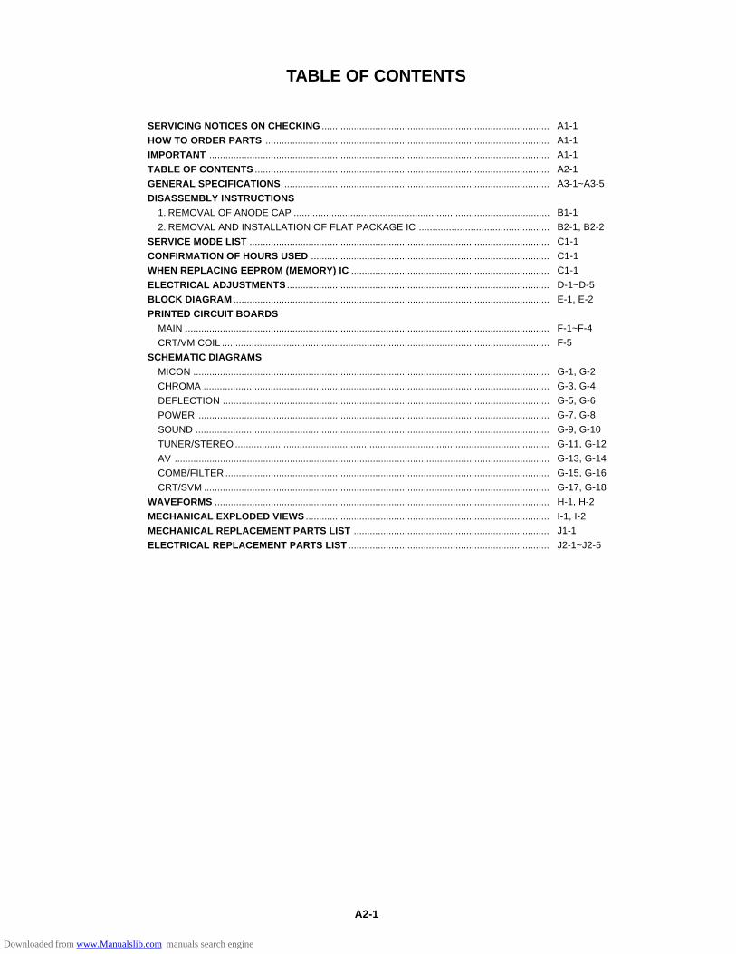
TABLE OF CONTENTS
SERVICING NOTICES ON CHECKING .....................................................................................
HOW TO ORDER PARTS ..........................................................................................................
IMPORTANT ...............................................................................................................................
TABLE OF CONTENTS ..............................................................................................................
GENERAL SPECIFICATIONS ...................................................................................................
DISASSEMBLY INSTRUCTIONS
1. REMOVAL OF ANODE CAP ...............................................................................................
2. REMOVAL AND INSTALLATION OF FLAT PACKAGE IC ................................................
SERVICE MODE LIST ................................................................................................................
CONFIRMATION OF HOURS USED .........................................................................................
WHEN REPLACING EEPROM (MEMORY) IC ..........................................................................
ELECTRICAL ADJUSTMENTS ..................................................................................................
BLOCK DIAGRAM ......................................................................................................................
PRINTED CIRCUIT BOARDS
MAIN ........................................................................................................................................
CRT/VM COIL ..........................................................................................................................
SCHEMATIC DIAGRAMS
MICON .....................................................................................................................................
CHROMA .................................................................................................................................
DEFLECTION ..........................................................................................................................
POWER ...................................................................................................................................
SOUND ....................................................................................................................................
TUNER/STEREO .....................................................................................................................
AV ............................................................................................................................................
COMB/FILTER .........................................................................................................................
CRT/SVM .................................................................................................................................
WAVEFORMS .............................................................................................................................
MECHANICAL EXPLODED VIEWS ...........................................................................................
MECHANICAL REPLACEMENT PARTS LIST .........................................................................
ELECTRICAL REPLACEMENT PARTS LIST ...........................................................................
A1-1
A1-1
A1-1
A2-1
A3-1~A3-5
B1-1
B2-1, B2-2
C1-1
C1-1
C1-1
D-1~D-5
E-1, E-2
F-1~F-4
F-5
G-1, G-2
G-3, G-4
G-5, G-6
G-7, G-8
G-9, G-10
G-11, G-12
G-13, G-14
G-15, G-16
G-17, G-18
H-1, H-2
I-1, I-2
J1-1
J2-1~J2-5
A2-1
Downloaded from www.Manualslib.com manuals search engine
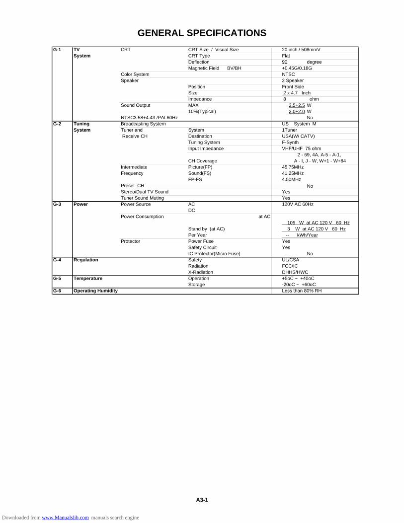
GENERAL SPECIFICATIONS
G-1 TV CRT CRT Size / Visual Size 20 inch / 508mmVSystem CRT Type Flat
Deflection 90 degreeMagnetic Field BV/BH +0.45G/0.18G
Color System NTSCSpeaker 2 Speaker
Position Front SideSize 2 x 4.7 InchImpedance 8 ohm
Sound Output MAX 2.5+2.5 W10%(Typical) 2.0+2.0 W
NTSC3.58+4.43 /PAL60Hz NoG-2 Tuning Broadcasting System US System M
System Tuner and System 1Tuner Receive CH Destination USA(W/ CATV)
Tuning System F-SynthInput Impedance VHF/UHF 75 ohm
2 - 69, 4A, A-5 - A-1, CH Coverage A - I, J - W, W+1 - W+84
Intermediate Picture(FP) 45.75MHzFrequency Sound(FS) 41.25MHz
FP-FS 4.50MHzPreset CH NoStereo/Dual TV Sound YesTuner Sound Muting Yes
G-3 Power Power Source AC 120V AC 60HzDC
Power Consumption at AC 105 W at AC 120 V 60 Hz
Stand by (at AC) 3 W at AC 120 V 60 HzPer Year -- kWh/Year
Protector Power Fuse YesSafety Circuit YesIC Protector(Micro Fuse) No
G-4 Regulation Safety UL/CSARadiation FCC/IC X-Radiation DHHS/HWC
G-5 Temperature Operation +5oC ~ +40oCStorage -20oC ~ +60oC
G-6 Operating Humidity Less than 80% RH
A3-1
Downloaded from www.Manualslib.com manuals search engine
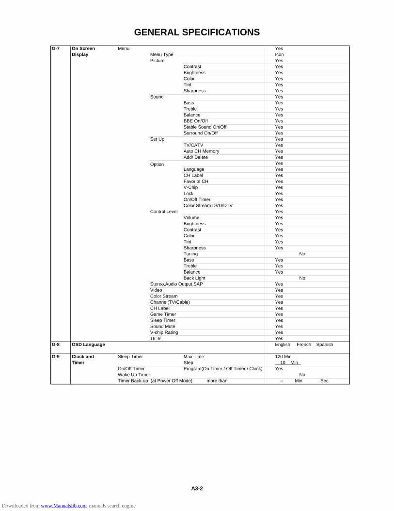
GENERAL SPECIFICATIONS
G-7 On Screen Menu YesDisplay Menu Type Icon
Picture YesContrast YesBrightness YesColor YesTint YesSharpness Yes
Sound YesBass YesTreble YesBalance YesBBE On/Off YesStable Sound On/Off YesSurround On/Off Yes
Set Up YesTV/CATV YesAuto CH Memory YesAdd/ Delete Yes
Option YesLanguage YesCH Label YesFavorite CH YesV-Chip YesLock YesOn/Off Timer YesColor Stream DVD/DTV Yes
Control Level YesVolume YesBrightness YesContrast YesColor YesTint YesSharpness YesTuning NoBass YesTreble YesBalance YesBack Light No
Stereo,Audio Output,SAP YesVideo YesColor Stream YesChannel(TV/Cable) YesCH Label YesGame Timer YesSleep Timer YesSound Mute YesV-chip Rating Yes16: 9 Yes
G-8 OSD Language English French Spanish
G-9 Clock and Sleep Timer Max Time 120 Min Timer Step 10 Min
On/Off Timer Program(On Timer / Off Timer / Clock) YesWake Up Timer NoTimer Back-up (at Power Off Mode) more than -- Min Sec
A3-2
Downloaded from www.Manualslib.com manuals search engine

GENERAL SPECIFICATIONS
G-10 Remote Unit RC-GWControl Glow in Dark Remocon Yes
Format Toshiba Custom Code TV:40-BF hPower Source Voltage(D.C) 3V
UM size x pcs UM-4 x 2 pcs Total Keys 50 KeysKeys Power Yes
1 Yes2 Yes3 Yes4 Yes5 Yes6 Yes7 Yes8 Yes9 Yes0 Yes100 YesCH Up YesCH Down YesVolume Up YesVolume Down YesTV/Caption/Text YesCH1/CH2 YesTV/Video(TV/AV) YesCH RTN/CH ENT(Quick View) YesSleep YesRE Call(Call) YesReset YesMenu/Enter YesMute YesExit YesMTS(Audio Select) YesFav.Up YesFav.Down Yes16: 9 Yes
Multi Brand Keys CH Up(VCR) YesCH Down(VCR) YesPause/Still YesTV/VCR(VCR) YesFF YesRew YesRec YesPlay YesStop YesTV YesVCR YesCable YesDVD YesCODE YesVolume Up(DVD) YesVolume Down(DVD) YesDVD CLEAR YesTOP MENU YesDVD MENU YesDISPLAY Yes
A3-3
Downloaded from www.Manualslib.com manuals search engine

GENERAL SPECIFICATIONS
G-11 Features Auto Degauss YesAuto Shut Off YesCanal+ NoCATV YesAnti-theft NoRental NoMemory(Last CH) YesMemory(Last Volume) YesV-Chip Yes
Type USA,Toshiba TypeBBE YesAuto Search NoCH Allocation NoSAP YesJust Clock Function NoCH Label YesVM Circuit YesFull OSD NoPremiere NoComb Filter Yes
3 LinesAuto CH Memory YesHotel Lock NoClosed Caption YesStable Sound YesFBT Leak Test Protect YesCH Lock YesVideo Lock YesGame Timer (Max Time:120 Min) YesEnergy Star NoFavorite CH YesSurround Yes16:9 Mode Yes
G-12 Accessories Owner's Manual Language English / FrenchW/ Warranty Yes
Remote Control Unit YesRod Antenna No
PolesTerminal
Loop Antenna NoTerminal -
U/V Mixer NoDC Car Cord (Center+) NoGuarantee Card NoWarning Sheet NoCircuit Diagram NoAntenna Change Plug NoService Station List NoImportant Safety Instruction NoDew/AHC Caution Sheet NoAC Plug Adapter NoQuick Set-up Sheet NoBattery Yes
UM size x pcs UM-4 x 2OEM Brand No
AC Cord NoAV Cord (2Pin-1Pin) NoRegistration Card (NDL Card) YesPTB Sheet NoESP Card No[From '04 MAR O/R]300 ohm to 75 ohm Antenna Adapter No
A3-4
Downloaded from www.Manualslib.com manuals search engine

GENERAL SPECIFICATIONS
G-13 Interface Switch Front Power YesSystem Select No Main Power SW No Sub Power No Channel Up YesChannel Down YesVolume Up YesVolume Down Yes
Rear AC/DC No TV/CATV Selector No Degauss No Main Power SW No
Indicator Power Yes(RED)Stand-by No On Timer No
Terminals Front Video Input = VIDEO3 RCA Audio Input = VIDEO3 RCA x 2 Other Terminal Head Phone
Rear Video Input(Rear1) = VIDEO1 RCA Video Input(Rear2) = VIDEO2 RCA Audio Input(Rear1) = VIDEO1 RCA x 2Audio Input(Rear2) = VIDEO2 RCA x 2Video Output RCA Audio Output RCA x 2Euro Scart NoColor Stream RCA x 3S Input YesDiversity NoExt Speaker NoDC Jack 12V(Center +) NoVHF/UHF Antenna Input F TypeAC Outlet No
G-14 Set Size Approx. W x D x H (mm) 590 x 484 x 446.5 G-15 Weight Net (Approx.) 23 kg ( 50.6 lbs)
Gross (Approx.) 26.5 kg ( 58.3 lbs)G-16 Carton Master Carton No
Content ---- SetsMaterial -- /--Dimensions W x D x H(mm) -- x -- x -- Description of Origin No
Gift Box YesMaterial Double/Brown Dimensions W x D x H(mm) 695 x 575 x 549 Design As per Buyer'sDescription of Origin Yes
Drop Test Natural Dropping At 1 Corner / 2Edges / 4 Surfaces
Height (cm) 60 (ORION SPEC:46)Container Stuffing 272 Sets/40' container
G-17 Cabinet Material Cabinet Cabinet Front PS 94V0 DECABROM Cabinet Rear PS 94V0 DECABROM
PCB Non-Halogen Demand NoEyelet Demand Yes
G-18 Environment Pb Free Lead-free Solder NoCd Free No
A3-5
Downloaded from www.Manualslib.com manuals search engine

B1-1
1. REMOVAL OF ANODE CAPRead the following NOTED items before starting work.
After turning the power off there might still be a potentialvoltage that is very dangerous. When removing theAnode Cap, make sure to discharge the Anode Cap'spotential voltage.Do not use pliers to loosen or tighten the Anode Capterminal, this may cause the spring to be damaged.
*
*
REMOVAL
1. Follow the steps as follows to discharge the Anode Cap.(Refer to Fig. 1-1.)Connect one end of an Alligator Clip to the metal part of aflat-blade screwdriver and the other end to ground.While holding the plastic part of the insulated Screwdriver,touch the support of the Anode with the tip of theScrewdriver.A cracking noise will be heard as the voltage is discharged.
Flip up the sides of the Rubber Cap in the direction of thearrow and remove one side of the support.(Refer to Fig. 1-2.)
2.
DISASSEMBLY INSTRUCTIONS
GND on the CRT
Screwdriver
Alligator Clip
SupportCRT
GND on the CRT
Rubber Cap
CRTSupport
Fig. 1-1
Fig. 1-2
3. After one side is removed, pull in the opposite direction toremove the other.
NOTE
Take care not to damage the Rubber Cap.
INSTALLATION
1. Clean the spot where the cap was located with a smallamount of alcohol. (Refer to Fig. 1-3.)
Location of Anode Cap
Fig. 1-3
NOTE
Confirm that there is no dirt, dust, etc. at the spot wherethe cap was located.
2.
3.
Arrange the wire of the Anode Cap and make sure thewire is not twisted.Turn over the Rubber Cap. (Refer to Fig. 1-4.)
Fig. 1-4
4. Insert one end of the Anode Support into the anode button,then the other as shown in Fig. 1-5.
5.6.
Confirm that the Support is securely connected.Put on the Rubber Cap without moving any parts.
CRTSupport
Fig. 1-5
Downloaded from www.Manualslib.com manuals search engine

B2-1
Masking Tape(Cotton Tape)
DISASSEMBLY INSTRUCTIONS
2.
REMOVAL
IC
Put the Masking Tape (cotton tape) around the FlatPackage IC to protect other parts from any damage.(Refer to Fig. 2-1.)
1.
Fig. 2-1
NOTE
REMOVAL AND INSTALLATION OFFLAT PACKAGE IC
Some ICs on the PCB are affixed with glue, so becareful not to break or damage the foil of each IC leadsor solder lands under the IC when removing it.
NOTE
Masking is carried out on all the parts located within 10mm distance from IC leads.
Blower type ICdesoldering machine
IC
Heat the IC leads using a blower type IC desolderingmachine. (Refer to Fig. 2-2.)
2.
Fig. 2-2
NOTE
Do not add the rotating and the back and forthdirections force on the IC, until IC can move back andforth easily after desoldering the IC leads completely.
When IC starts moving back and forth easily afterdesoldering completely, pickup the corner of the IC using atweezers and remove the IC by moving with the ICdesoldering machine. (Refer to Fig. 2-3.)
3.
Blower type ICdesolderingmachine
IC
Fig. 2-3
Tweezers
Peel off the Masking Tape.4.
Absorb the solder left on the pattern using the BraidedShield Wire. (Refer to Fig. 2-4.)
5.
NOTE
Do not move the Braided Shield Wire in the verticaldirection towards the IC pattern.
Braided Shield Wire
Soldering Iron
Fig. 2-4IC pattern
Downloaded from www.Manualslib.com manuals search engine

B2-2
DISASSEMBLY INSTRUCTIONS
Supply solderingfrom upper positionto lower position
IC
Supply the solder from the upper position of IC leadssliding to the lower position of the IC leads. (Refer to Fig. 2-6.)
2.
Fig. 2-6
Soldering IronSolder
IC
Absorb the solder left on the lead using the Braided ShieldWire. (Refer to Fig. 2-7.)
3.
Fig. 2-7
Soldering Iron
Braided Shield Wire
NOTE
Do not absorb the solder to excess.
IC
Fig. 2-8
Thin-tip Soldering Iron
NOTE
When the IC leads are bent during soldering and/orrepairing, do not repair the bending of leads. If thebending of leads are repaired, the pattern may bedamaged. So, always be sure to replace the IC in thiscase.
Finally, confirm the soldering status on four sides of the ICusing a magnifying glass.Confirm that no abnormality is found on the solderingposition and installation position of the parts around the IC.If some abnormality is found, correct by resoldering.
5.Solder temporarily
Soldering Iron
INSTALLATION
Take care of the polarity of new IC and then install the newIC fitting on the printed circuit pattern. Then solder eachlead on the diagonal positions of IC temporarily.(Refer to Fig. 2-5.)
1.
Fig. 2-5
Solder temporarily
4. When bridge-soldering between terminals and/or thesoldering amount are not enough, resolder using a Thin-tip Soldering Iron. (Refer to Fig. 2-8.)
Downloaded from www.Manualslib.com manuals search engine

SERVICE MODE LISTThis unit provided with the following SERVICE MODES so you can repair, examine and adjust easily.To enter the Service Mode, press both set key and remote control key for more than 1 second.
Set Key Remocon Key Operations
VOL. (-) MIN 0 Releasing of V-CHIP PASSWORD.
VOL. (-) MIN 1
Initialization of the factory.NOTE: Do not use this for the normal servicing.
If you set a factory initialization, the memories are reset such as the channel setting,and the POWER ON total hours.
VOL. (-) MIN 6
POWER ON total hours is displayed on the screen.Refer to the "CONFIRMATION OF HOURS USED".
Can be checked of the INITIAL DATA of MEMORY IC.Refer to the "WHEN REPLACING EEPROM (MEMORY) IC".
VOL. (-) MIN 8 Writing of EEPROM initial data.NOTE: Do not use this for the normal servicing.
VOL. (-) MIN Display of the Adjustment MENU on the screen.Refer to the "ELECTRICAL ADJUSTMENT" (On-Screen Display Adjustment).
9
CONFIRMATION OF HOURS USEDPOWER ON total hours can be checked on the screen. Total hours are displayed in 16 system of notation.NOTE: If you set a factory initialization, the total hours is reset to "0".1.2.
3.
Set the VOLUME to minimum.Press both VOL. DOWN button on the set and Channelbutton (6) on the remote control for more than 1 second.After the confirmation of using hours, turn off the power.
ADDRESS DATA
INIT 00 50CRT ON 0010
FIG. 1
Initial setting content of MEMORY IC.POWER ON total hours. = (16 x 16 x 16 x thousands digit value) + (16 x 16 x hundreds digit value) + (16 x tens digit value) + (ones digit value)
C-1
WHEN REPLACING EEPROM (MEMORY) ICIf a service repair is undertaken where it has been required to change the MEMORY IC, the following steps should be taken toensure correct data settings while making reference to TABLE 1.
Table 11.2.
3.
4.5.6.7.8.
9.10.11.The unit will now have the correct DATA for the new MEMORY IC.
Enter DATA SET mode by setting VOLUME to minimum.Press both VOL. DOWN button on the set and Channel button (6) on the remote control for more than 1 second.ADDRESS and DATA should appear as FIG 1.ADDRESS is now selected and should "blink". Using the VOL. UP/DOWN button on the remote, step through the ADDRESSuntil required ADDRESS to be changed is reached.Press ENTER to select DATA. When DATA is selected, it will "blink".Again, step through the DATA using VOL. UP/DOWN button until required DATA value has been selected.Pressing ENTER will take you back to ADDRESS for further selection if necessary.Repeat steps 3 to 6 until all data has been checked.When satisfied correct DATA has been entered, turn POWER off (return to STANDBY MODE) to finish DATA input.After the data input, set to the initializing of shipping.Turn POWER on.Press both VOL. DOWN button on the set and Channel button (1) on the remote control for more than 1 second.After the finishing of the initializing of shipping, the unit will turn off automatically.
NOTE: No need setting for after INI 1F due to the adjustment value.
50 E8 0A 45 5E B3 24 B7 3D AC
+0 +1 +2 +3 +4 +5 +6 +7 +8 +9 +A +B +C +D +E +FINI
50 00 00 00 00 00 00 3F 0F10 00 0D E2 94 88 3F 00
00 0A 04 40 40 40 7F
Downloaded from www.Manualslib.com manuals search engine

ELECTRICAL ADJUSTMENTS
D-1
1.
Read and perform these adjustments when repairing thecircuits or replacing electrical parts or PCB assemblies.
CAUTION
Use an isolation transformer when performing any serviceon this chassis.Before removing the anode cap, discharge electricitybecause it contains high voltage.When removing a PCB or related component, afterunfastening or changing a wire, be sure to put the wireback in its original position.When you exchange IC and Transistor for a heat sink, applythe silicon grease on the contact section of the heat sink.Before applying new silicon grease, remove all the oldsilicon grease. (Old grease may cause damages to the ICand Transistor.)
BEFORE MAKING ELECTRICALADJUSTMENTS
Prepare the following measurement tools for electricaladjustments.
•
•
•
•
1. Oscilloscope2. Digital Voltmeter3. Multi-sound Generator4. Pattern Generator
On-Screen Display Adjustment
In the condition of NO indication on the screen.Press the VOL. DOWN button on the set and the Channelbutton (9) on the remote control for more than 1 second toappear the adjustment mode on the screen as shown inFig. 1-1.
1.
Fig. 1-1
Use the Channel UP/DOWN button or Channel button (0-9) on the remote control to select the options shown inFig. 1-2.Press the MENU button on the remote control to end theadjustments.
2.
3.
FUNCTIONOSD HCUT OFFH.VCOH.PHASEAFC GAINV.SHIFTH.SIZEV.SIZEV.LINEARITYVS CORRECTIONDRIVE RDRIVE BR CUT OFF
NO.00010203040506070809101112
Fig. 1-2
FUNCTIONG CUT OFFB CUT OFFBRIGHT MAXBRIGHT CENTBRIGHT MINCONTRAST MAXCONTRAST CENTCONTRAST MINCOLOR MAXCOLOR CENTCOLOR MINTINTSHARPNESS
NO.13141516171819202122232425
TV
00 OSD 25
2. BASIC ADJUSTMENTS
2-2: CUT OFF
1.2.
3.
Place the set with Aging Test for more than 15 minutes.Activate the adjustment mode display of Fig. 1-1 andpress the channel button (01) on the remote control toselect "CUT OFF".Adjust the Screen Volume until a dim raster is obtained.
2-3: WHITE BALANCE
NOTE: Adjust after performing CUT OFF adjustment.
1.2.3.
4.
5.
6.
7.
Place the set with Aging Test for more than 10 minutes.Receive the gray scale pattern from the Pattern Generator.Using the remote control, set the brightness and contrastto normal position.Activate the adjustment mode display of Fig. 1-1 andpress the channel button (10) on the remote control toselect “R. DRIVE”.Press the CH. UP/DOWN button on the remote control toselect the “R. BIAS”, “G. BIAS”, “B. BIAS”, “R. DRIVE” or“B. DRIVE”.Adjust the VOL. UP/DOWN button on the remote controlto whiten the R. BIAS, G. BIAS, B. BIAS, R. DRIVE, andB. DRIVE at each step tone sections equally.Perform the above adjustments 5 and 6 until the whitecolor is looked like a white.
2-4: FOCUS
1.2.3.
Receive a broadcast.Turn the Focus Volume fully counterclockwise once.Adjust the Focus Volume until picture is distinct.
2-1: CONSTANT VOLTAGE
1.2.3.
4.5.
Place the set with Aging Test for more than 5 minutes.Set condition is AV MODE without signal.Using the remote control, set the brightness and contrastto normal position.Connect the digital voltmeter to the TP003.Adjust the VR502 until the digital voltmeter is 115 ± 1V.
FUNCTIONCB DELAY FINECR DELAY FINECB PEDESTAL ADJCR PEDESTAL ADJE/W PARABOLAE/W CORNERE/W TRAPEZIUMLEVELSEPARATION 1SEPARATION 2
NO.262728293031.32.33.34.35.
2-5: HORIZONTAL PHASE
1.2.
3.
4.
Receive the monoscope pattern.Using the remote control, set the brightness and contrastto normal position.Activate the adjustment mode display of Fig. 1-1 andpress the channel button (03) on the remote control toselect "H.PHAS".Press the VOL. UP/DOWN button on the remote controluntil the SHIFT quantity of the OVER SCAN on right andleft becomes minimum.
2-6: VERTICAL POSITION
1.2.
3.4.
Receive the monoscope pattern.Using the remote control, set the brightness and contrastto normal position.Check if the step No. V. SHIFT is "02".Adjust the VR401 until the horizontal line becomes fit tothe notch of the shadow mask.
Downloaded from www.Manualslib.com manuals search engine
ELECTRICAL ADJUSTMENTS
D-2
2-7: VERTICAL SIZE
1.2.
3.
4.
5.
Receive the monoscope pattern.Using the remote control, set the brightness andcontrast to normal position.Activate the adjustment mode display of Fig. 1-1 andpress the channel button (07) on the remote control toselect "V.SIZE".Press the VOL. UP/DOWN button on the remote controluntil the SHIFT quantity of the OVER SCAN on upside anddownside becomes 9 ± 2%.Receive a broadcast and check if the picture is normal.
2-8: VERTICAL LINEARITY
NOTE: Adjust after performing adjustments in section 2-7.After the adjustment of Vertical Linearity, reconfirmthe Vertical Position and Vertical Size adjustments.
Receive the monoscope pattern.Using the remote control, set the brightness and contrastto normal position.Activate the adjustment mode display of Fig. 1-1 andpress the channel button (08) on the remote control toselect "V.LIN".Press the VOL. UP/DOWN button on the remote controluntil the SHIFT quantity of the OVER SCAN on upsideand downside becomes minimum.
1.2.
3.
4.
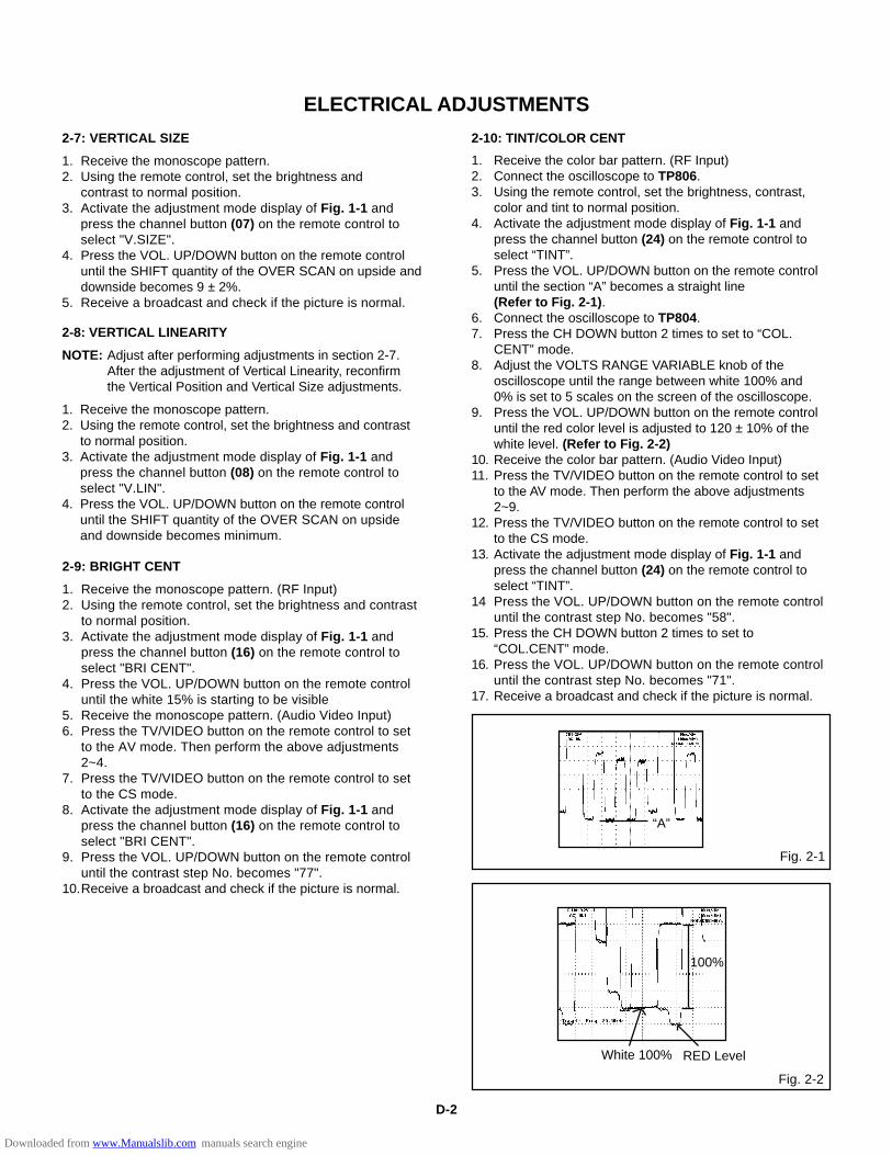
2-10: TINT/COLOR CENT
1.2.3.
4.
5.
6.7.
8.
9.
10.11.
12.
13.
14
15.
16.
17.
Fig. 2-1
Receive the color bar pattern. (RF Input)Connect the oscilloscope to TP806.Using the remote control, set the brightness, contrast,color and tint to normal position.Activate the adjustment mode display of Fig. 1-1 andpress the channel button (24) on the remote control toselect “TINT”.Press the VOL. UP/DOWN button on the remote controluntil the section “A” becomes a straight line(Refer to Fig. 2-1).Connect the oscilloscope to TP804.Press the CH DOWN button 2 times to set to “COL.CENT” mode.Adjust the VOLTS RANGE VARIABLE knob of theoscilloscope until the range between white 100% and0% is set to 5 scales on the screen of the oscilloscope.Press the VOL. UP/DOWN button on the remote controluntil the red color level is adjusted to 120 ± 10% of thewhite level. (Refer to Fig. 2-2)Receive the color bar pattern. (Audio Video Input)Press the TV/VIDEO button on the remote control to setto the AV mode. Then perform the above adjustments2~9.Press the TV/VIDEO button on the remote control to setto the CS mode.Activate the adjustment mode display of Fig. 1-1 andpress the channel button (24) on the remote control toselect “TINT”.Press the VOL. UP/DOWN button on the remote controluntil the contrast step No. becomes "58".Press the CH DOWN button 2 times to set to“COL.CENT” mode.Press the VOL. UP/DOWN button on the remote controluntil the contrast step No. becomes "71".Receive a broadcast and check if the picture is normal.
“A”
Fig. 2-2
2-9: BRIGHT CENT
1.2.
3.
4.
5.6.
7.
8.
9.
10.
Receive the monoscope pattern. (RF Input)Using the remote control, set the brightness and contrastto normal position.Activate the adjustment mode display of Fig. 1-1 andpress the channel button (16) on the remote control toselect "BRI CENT".Press the VOL. UP/DOWN button on the remote controluntil the white 15% is starting to be visibleReceive the monoscope pattern. (Audio Video Input)Press the TV/VIDEO button on the remote control to setto the AV mode. Then perform the above adjustments2~4.Press the TV/VIDEO button on the remote control to setto the CS mode.Activate the adjustment mode display of Fig. 1-1 andpress the channel button (16) on the remote control toselect "BRI CENT".Press the VOL. UP/DOWN button on the remote controluntil the contrast step No. becomes "77".Receive a broadcast and check if the picture is normal.
White 100% RED Level
100%
Downloaded from www.Manualslib.com manuals search engine

ELECTRICAL ADJUSTMENTS
D-3
Activate the adjustment mode display of Fig. 1-1 andpress the channel button (18) on the remote control toselect "CONT.MAX".Press the VOL. UP/DOWN button on the remote controluntil the contrast step No. becomes "86".Receive a broadcast and check if the picture is normal.Press the TV/VIDEO button on the remote control to setto the AV mode. Then perform the above adjustments1~3.Press the TV/VIDEO button on the remote control to setto the CS mode. Then perform the above adjustments1~3.
1.
2.
3.4.
5.
2-11: CONTRAST MAX MANUAL
2-12: SEPARATION 1, 2
Please do the method (1) or method (2) adjustment.
Method (1)
1.
2.3.
4.
5.
Set the multi-sound signal generator for each different L-ch and R-ch frequency (Ex. L-ch=2KHz, R-ch=400Hz) andreceive the RF.Connect the oscilloscope to the Audio Out Jack.Activate the adjustment mode display of Fig. 1-1 andpress the channel button (34) on the remote control toselect “SEP 1”.Press the VOL. UP/DOWN button on the remote control toadjust it until the audio output wave becomes a fine sinewave.Press the CH UP button once the set to “SEP 2” mode.Then perform the above adjustment 4.
Method (2)
1.
2.3.
4.
5.
6.
7.8.
9.
Set the multi-sound signal generator L-ch=1KHz, R-ch=Non input and receive the RF.Connect the oscilloscope to the Audio Out Jack (R-ch).Press the AUDIO SELECT button on the remote control toset to the stereo mode.Activate the adjustment mode display of Fig. 1-1 andpress the channel button (34) on the remote control toselect “SEP 1”.Press the VOL. UP/DOWN button on the remote control toadjust it until the R-ch output becomes minimum.Set the multi-sound signal generator L-ch=Non input,R-ch=1KHz and receive the RF.Connect the oscilloscope to the Audio Out Jack (L-ch).Activate the adjustment mode display of Fig. 1-1 andpress the channel button (35) on the remote control toselect “SEP 2”.Press the VOL. UP/DOWN button on the remote control toadjust it until the L-ch output becomes minimum.
2-13: LEVEL
1.2.3.
4.
Receive the monoscope pattern (70dB).Connect the AC voltmeter to pin 6 of CP101.Activate the adjustment mode display of Fig. 1-1 andpress the channel button (33) on the remote control toselect "LEVEL".Press the VOL. UP/DOWN button on the remote controluntil the AC voltmeter is 85 ± 2mV.
Please check if the fixed values of the each adjustmentitems are set correctly referring below.
2-14: Confirmation of Fixed Value (step No.)
NO.000204050609151719202123252627303132
FUNCTIONOSD HH.VCOAFC GAINV.SHIFTH.SIZEVS CORRECTIONBRIGHT MAXBRIGHT MINCONTRAST CENTCONTRAST MINCOLOR MAXCOLOR MINSHARPNESSCB DELAY FINECR DELAY FINEE/W PARABOLAE/W CORNERE/W TRAPEZIUM
STEP NO.2503070201341257550189000400000313131
Downloaded from www.Manualslib.com manuals search engine
ELECTRICAL ADJUSTMENTS
D-4
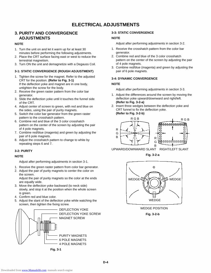
3. PURITY AND CONVERGENCEADJUSTMENTS
NOTE
1.
2.
3.
Turn the unit on and let it warm up for at least 30minutes before performing the following adjustments.Place the CRT surface facing east or west to reduce theterrestrial magnetism.Turn ON the unit and demagnetize with a Degauss Coil.
3-1: STATIC CONVERGENCE (ROUGH ADJUSTMENT)
1.
2.
3.
4.
5.
6.
7.
8.
Tighten the screw for the magnet. Refer to the adjustedCRT for the position. (Refer to Fig. 3-1)If the deflection yoke and magnet are in one body,untighten the screw for the body.Receive the green raster pattern from the color bargenerator.Slide the deflection yoke until it touches the funnel sideof the CRT.Adjust center of screen to green, with red and blue onthe sides, using the pair of purity magnets.Switch the color bar generator from the green rasterpattern to the crosshatch pattern.Combine red and blue of the 3 color crosshatchpattern on the center of the screen by adjusting the pairof 4 pole magnets.Combine red/blue (magenta) and green by adjusting thepair of 6 pole magnets.Adjust the crosshatch pattern to change to white byrepeating steps 6 and 7.
3-2: PURITY
NOTE
Adjust after performing adjustments in section 3-1.
1.2.
3.
4.5.
Receive the green raster pattern from color bar generator.Adjust the pair of purity magnets to center the color onthe screen.Adjust the pair of purity magnets so the color at the endsare equally wide.Move the deflection yoke backward (to neck side)slowly, and stop it at the position when the whole screenis green.Confirm red and blue color.Adjust the slant of the deflection yoke while watching thescreen, then tighten the fixing screw.
DEFLECTION YOKEDEFLECTION YOKE SCREWMAGNET SCREW
PURITY MAGNETS6 POLE MAGNETS4 POLE MAGNETS
Fig. 3-1
3-3: STATIC CONVERGENCE
NOTE
Adjust after performing adjustments in section 3-2.
1.
2.
3.
Receive the crosshatch pattern from the color bargenerator.Combine red and blue of the 3 color crosshatchpattern on the center of the screen by adjusting the pairof 4 pole magnets.Combine red/blue (magenta) and green by adjusting thepair of 6 pole magnets.
3-4: DYNAMIC CONVERGENCE
NOTE
Adjust after performing adjustments in section 3-3.
1.
2.
Adjust the differences around the screen by moving thedeflection yoke upward/downward and right/left.(Refer to Fig. 3-2-a)Insert three wedges between the deflection yoke andCRT funnel to fix the deflection yoke.(Refer to Fig. 3-2-b)
R G B
RGB R
GB
R G B
UPWARD/DOWNWARD SLANT RIGHT/LEFT SLANT
Fig. 3-2-a
WEDGE WEDGE
WEDGE
WEDGE POSITION
Fig. 3-2-b
Downloaded from www.Manualslib.com manuals search engine

W003
CP502
TP003
VR502
CP101
CP801A
J704 J702
J1001J705 J706 J707
CP1001OS101
CP802A
CP851A
VR401
J701J703J708
SPEAKER
CRT
FB401
TU
001
CP501
AC IN
CD
501
CRT
CP852B
CP803
CP804T
P806
TP
804
R808
R804
CP852
CP851B
CP802B CP801B
J801
CRT
CRT PCB
VM COIL PCB
MAIN PCB
CD
803
CD852
CD801
CD802
CD851
CD1001
ELECTRICAL ADJUSTMENTS
4. ELECTRICAL ADJUSTMENT PARTS LOCATION GUIDE (WIRING CONNECTION)
D-5
Downloaded from www.Manualslib.com manuals search engine
3
2
7
5
1
HEADPHONE_JACKJ1001
SPEAKERSP1001
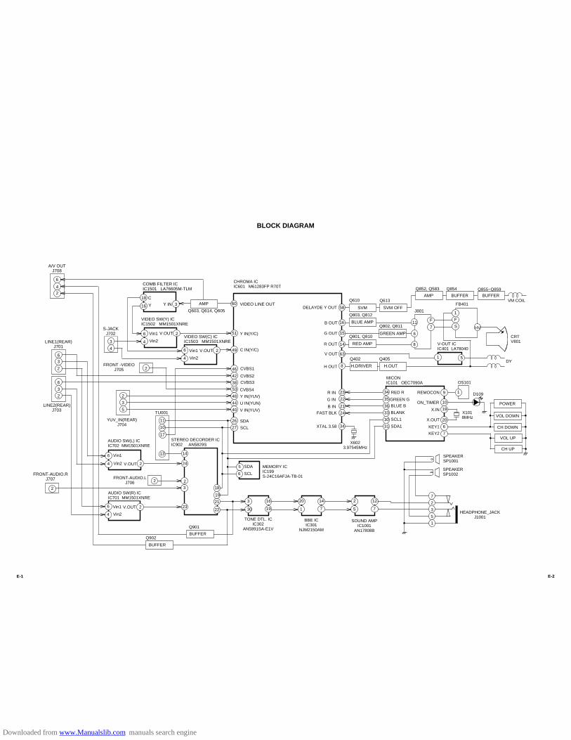
BLOCK DIAGRAM
CHROMA ICIC601 M61283FP R70T
VIDEO LINE OUT60
Y IN(Y/C)51
42
49
53
38
48
CVBS1
C IN(Y/C)
CVBS2
CVBS3
CVBS4
Y IN(YUV)
44 U IN(YUN)
X1018MHz
D1091
OS101
23R IN
VOL UP
46
VOL DOWN
CH DOWN
MICONIC101 OEC7090A
B IN 21
35 GREEN G
36 BLUE B
J801
6
11
8
F
7
DY
G IN 22
34 RED R
40 V IN(YUV)
POWER
8
63V OUT
H OUT
FAST BLK 24
V-OUT ICIC401 LA78040
CRTV801
15
16
14
B OUT
G OUT
R OUT
33 BLANK
Q803, Q812
BLUE AMPQ802, Q811
GREEN AMPQ801, Q810
RED AMP
FB401
Q405Q402
H.OUTH.DRIVER
51
18
16 3
COMB FILTER ICIC1501 LA76605M-TLM
C
Y Y IN
4
2
VIDEO SW(Y) ICIC1502 MM1501XNRE
Vin1
Vin2
V.OUT
2
VIDEO SW(C) ICIC1503 MM1501XNRE
6
4
6 Vin1
Vin2
V.OUT
3
S-JACKJ702
4
LINE1(REAR)J701
6
LINE2(REAR)J703
6
FRONT -VIDEOJ705 2
2
YUV_IN(REAR)J704
3
5
2
STEREO DECORDER ICIC902 AN5829S
24
14
23
3
6
4 2
AUDIO SW(L) ICIC702 MM1501XNRE
Vin1
Vin2 V.OUT
FRONT-AUDIO.LJ706
FRONT-AUDIO.RJ707
2
3
2
3
2
6
4
2
AUDIO SW(R) ICIC701 MM1501XNRE
Vin1
Vin2
V.OUT
2
3
30 19
TONE DTL. ICIC302
AN5891SA-E1V
16 20
1 7
BBE ICIC301
NJM2150AM
14 2
5 7
SOUND AMPIC1001
AN17808B
12
SPEAKERSP1002
21
22
Q901
BUFFERQ902
BUFFER
TU001
17
13
11
10 27 SCL
26 SDA
6
5 MEMORY ICIC199S-24C16AFJA-TB-01
SCL
SDA
30 SCL1
31 SDA1
10ON_TIMER
6KEY1
7KEY2
9REMOCON
19X.IN
20X.OUT
CH UP
X6023.97545MHz
34XTAL 3.58
58DELAYDE Y OUT
Q610
SVM
Q613
SVM OFF
Q852, Q583
AMP
Q854
BUFFER
18
19
VM COIL
Q855~Q859
A/V OUTJ708
42
6
Q603, Q614, Q605
AMP
BUFFER
1
F
S HV
E-1 E-2
Downloaded from www.Manualslib.com manuals search engine

CP507
Q514
D524
R543
D507
R544
B403
R545
CP508
C503
C502
Q402
D411
W004
W007
W003
W006
W801
B501
T501
FH502 F501 FH501
CP501
CP
502
D502
D503
D501
R500
D523
RY501
C506_1
R520
R540
R501
L501C505_1
D516
R503
C403
C504
D505 D520
Q504
B504
C527
C520
C501
D511D406
B401
B402
W002
W010
W018
R452_1
C517
R430
C408
R429
R433
R416
R413
R420
CP401R427
TP003
R443
R437
R441
R414 R428
W020IC401
R432
R43
9
C426
D404
D415
D410D403
W019
R527
R506
D528
Q507
R553
R554
VR502
CP101
D402
HS402
C425
TP004
CP801A
FB401
C418
C420_1
L402_1
W011
W009
W071
R406
R421
IC504
W001
C409
C539_1
C430
C407
C406
R502
D506
Q502
R542
C509
HS501
W005
D414
R547
D525
W825
R517_1
L401
C410
D504
R434
Q503R507
R536
R535
R505
W806
D517
D513
R512
R410_1
T401_1
J704J702
J1001
J705J706J707
W179
W177
W178
CP1001R1001
R1002
R537
C904
C905
C907
C916
W119
C910
C914
L901
C903
C902
C901
W092
R905
R904
R901
R902
W125
W174
W175
L301
C302
C306
R301
C305C
308
C314
C316
C318
R302
C333
C304
SW105
R120 O
S101
C108
D109
SW102
R515
R118
W053 W
822
W120
C122
C110
R139
R140
SW103 SW104 SW101
R102
W128
W129
R119
W118W121
W122
D105
C109
W126
D104
W055
C113
D106
W049
R133
W052
W056
W093
W116
C317
C319
C321
W181
C332
R313
W180
C329
C327
Q405
C330
C328
W160
D608
W028
W176
R002
R001
W027
W101
W109
W098
C535
R539
W161
CP802A
CP
851A
W023
W041
W099
W114
W102
W104
W106
W112
R124
W094
W111
W044
TU
001
D001
D709
W062
W133
C701
C702
C728
R710
C711
C707
C708
C1004
C1007
C1009
C1008
IC1001 HS1001
R1009
W803
W136
W137
W130
C1005
W138
W072
W134
W060
C1518C
1510
L1505
L1503
L1502
L1508
C1520
C1501
C1502
L1511
C1528
L1510
C1525
W156
W858
W166
W077
W076
C001_1
L1501
C1532W146
W145
C642
C605
D602D601
R603
D603
W162
X602
C630
C627
C622
Q607
W075
W058
W070
W073W
108
W107
W030
C621
W061
W069
C618
W067
W090
C611
Q606
Q604
Q602
C610
R649
C603
W059
R616
W151
W150
W147
W144
W173
Q601
Q611
C602R601
C606
W172
W082
R132
W029
W103
W096
W113
W805
W168
L1512
R626
R623
W097
W167
W170
W100
W139
C615
W115
C413_1
D509
R508
TP006
TP005
W171
D604
D514W043
W132
W804
C1003
W074
C919
C1001_1
C1002_1
C710
D407
W850
W813
C114
W021
VR
401R422
R418
W143
W088
W089
W068
W054
R146
D510
W812
C733
D701
D703
D702
W079
B405
C1535
W148W
149
W154
R602
C609
W155
R510
W013
C608R648
W140
R303
R304
C601
W163
C623
L601
W164
W165
D706
W117
W095
W080
W022
W025
W048
D705D704
W091
W123
R130
W127
W124
W159
W157
C139
W033
J701 J703 J708
W035
W032
W037
W038W
040
W064W
063
W135
R546
R702
C645
W081
W083
R701
C705
C629
W045W046
D607
D605
D606
W169
C1530
W026W084
W131
W835
TH
501_2
C402
C415_1
C417
C508_1
C512
C513_1
C519_1
C524
D107
D108
D110
D512
R426
R436
W821
W065
W078
W057
W183
C427
C521
W185
W110
W042
W024
C1011_1
W039
W186
D508
R524
W187
C550
W188
Q505
Q508
Q509
Q512
R438
R541_1
C507
X101_1
C638
D113
D405
W141
W008
W861
W184
W142
W087
R402
W811
W844
W819
W820
W815
W829
W830
W817
W848
CD801A
CD802A
W860
PRINTED CIRCUIT BOARDSMAIN (INSERTED PARTS)
SOLDER SIDE
F-1 F-2
6.3A125VOR250V
_A_V
Downloaded from www.Manualslib.com manuals search engine

17
33
49
1
C54
1
R45
3
R52
5C51
1
R40
3
R417 R41
5
C40
5
R53
2R
533
C55
4
R407
R513
R511
R404
R74
5C74
1
C74
2
R74
6
C720C719
R724
IC902
C90
8
C91
2C
915
C91
8 R907
Q902
R906
Q901
R90
3
C917
C913
C911
R91
2
IC302
C303
C312
C301
R31
4
R10
3
R10
6
R13
8
R13
5
C128
IC199_1
R12
2
IC101
R112
R11
0
C13
1R131
C11
7C
121
R128
R14
2 R12
9
R12
6
C102C104
R113
C106
R136
C11
9C
111
R101
R11
4
Q101
R109
R125
C12
0
R150
Q103
R12
7R
141
R14
3
C13
5
R14
5
C115
C30
9C
307
C31
0C
313
C32
2
C32
0
IC301
R31
2
R31
0R
309
C32
5R
307
C323
R30
5
C32
6R
308
C32
4R
306
IC60
1
C439
R516
C002
C73
4R
735R73
9C73
6
C73
8
R73
3R
729
R72
6
C72
5
C72
2
R73
4
R72
7C
735
R72
8 C72
4C
727
C73
7
IC701IC702
C70
6
R73
0
R736
R72
1
Q712
Q711
R71
1
R70
8R
725
R70
4
R70
6
R705
R1013
Q1001
R10
03R1011
R10
04
R1010C1010 C1012
Q709R70
9
R006
IC1503IC1502
C1512C1516
R1529
R15
28
R15
05
Q1503
C15
13C
1517
R15
06
R1507
C15
19
C15
09
C15
15
C15
04
R15
04
C1514
R1503
C15
06
C1507
IC1501
C15
03
R15
02C
1521
C15
08
R1508
Q1504
R15
09
R1510
C15
31
Q1508
R15
30C
1505 Q1507
R15
16 C1526
R15
18
R1519
C15
23
C64
1
R15
20C
1533
R63
2
C136 C137 C138
C63
2
R61
8
C63
1
C62
4
C61
4 R610
C60
7
R61
7
C640
R628
Q603
R60
4
R62
5
R1523
R609
R62
9
R62
2
R63
4
R62
0
C61
2C61
6
R61
1
R641R635C628
R612
R63
6
R70
3
C00
5
R15
22
R31
1
R40
1
R1512
Q605
R607
R60
5
R60
8R
606
Q614
C31
5C
311
C33
4
R61
9
R621
R64
2
R62
4R
643
R644
C62
5
Q610
R64
5C
633
R653R652
R61
3C
635
R65
1
C64
4C
643
C63
7
C14
0
C14
1
C14
5
Q613
C63
4
R64
7
R64
6C
604
C14
4
C14
2
C14
3
R519
R13
4
R62
7
C14
6
C41
1
C61
9
R65
4
R40
9_1
R137
C636
C416
PRINTED CIRCUIT BOARDSMAIN (CHIP MOUNTED PARTS)
SOLDER SIDE
F-3 F-4
Downloaded from www.Manualslib.com manuals search engine

CP803
CP
804
TP805
TP806
TP804
D801
D802
D803
Q812
Q811
Q810
R830
R828
R829
R808
R804
R806
Q802
Q803
Q801
R818
C813
B852
Q856
Q855
Q857
Q854
Q852
Q853
R881
C854
R879
R878
B851
C865
C864
R877
R880
C853
C852
R857
C860
C861
D852
J801
R872
D855
R869
R875
R871
D856
R866
D853
R868
R873
R874
R876
R870
R867
L802
L803
L804
C862_1
C863_1
D858
D857
W006
W004
D854
W009
B853
C858
C859Q858
Q859
HS
851
CP
852B
S851
S852
C821_1
R814R
813
R810
R815
R809
R811
C804R
817
C806
R821
R819C805
R812
R862
R863
R865
R864
C857
R858
R861
R860
C855
R854
C856
R859
R856
R853
CP852
W806
R855
D804
D805
W001
D807
D809
W805
W007
CP
851B
CP
802BC
P801B
D808
W008
W811
W003
C809
D806
R822
W820
R820
C808
W804
W810
W808
W807
W809
W802
PRINTED CIRCUIT BOARDSCRT/VM COIL
SOLDER SIDE
F-5
Downloaded from www.Manualslib.com manuals search engine
A B C D E F G H
A B C D E F G H
2
1
3
4
5
6
7
8
2
1
3
4
5
6
7
8
OF PRINTING AND SUBJECT TO CHANGE WITHOUT NOTICENOTE:THIS SCHEMATIC DIAGRAM IS THE LATEST AT THE TIME
WAS RECEIVED IN GOOD CONDITION AND PICTURE IS NORMAL.WITH THE DIGITAL TESTER WHEN THE COLOR BROADCAST
NOTE:THE DC VOLTAGE AT EACH PART WAS MEASURED
R134
10K
R110
10K
R119
22K 1/4W
R138
1M
R114
47K
R112
2.2KR113
2.2K
R109
1K
R118
2.2K 1/4W
R133
1K 1/4W
R146
100
1/4W
R136 4.7K
R135 4.7K
R124
1K1/
4W
R145
2.2KR1
43
1.5KR1
42
1.5KR1
41
1.5K
R127
6.8KR128
6.8KR129
6.8K
R101
560R103
2.7K
R106
560
R120
471/
4W
R102
270
1/4W
R122 1K
R150
1K
R140
100 1/4W
R139
100 1/4W
R130
47K 1/4W
R126
100
R125
10
R131
1K
R137
10K
R132
100 1/4W
C138
0.1
B
C137
0.1
B
C135
10P
CH
C144
150P CH
C115
820P CH
C121
0.01 B
C109
0.1 B
C131
150P CH
C128
0.1 F
C106
0.1
B
C140
220P CHC141
220P CH
C142
220P CH
C143
220P CH
C146
33P CH
C102 27P CH
C104 27P CH
C145
220P CH
C120
0.001 B
C117
47P CH
C119
220P CH
C111
0.001 B
C113
0.1 B
C136
0.1
B
W811
W822
D106
MTZ
J5.1
B
D113
MTZ
J5.6
B
C108
1016
VKA
C110
2200
6.3V
YK
C139 10
16V
KA
C122
150V KA
C114
0.47
50V
KAD1
10
1SS1
33
D105
1SS133
D104
1SS133
D108
1SS1
33
D107
1SS1
33
Q101KTC3875S_Y_RTK
LED SW
Q103KTC3875S_Y_RTK
CLAMP SW
IC19
9_1
S-24
C16A
FJA-
TB-0
1
MEM
ORY
IC
1234
5 6 7 8
X101_1100CT8R005
8MHz
SW10
1EV
Q215
05R
CH U
P
SW10
3EV
Q215
05R
VOL
UP
SW10
2EV
Q215
05R
CH D
OWN
SW10
4EV
Q215
05R
VOL
DOW
N
SW10
5EV
Q215
05R
POW
ER
D109
SLR-
342V
CT32
POW
ER O
N
CP101 173979-7
1
2
3
4
5
6
7
TM101R25-1943
BT001R03(AB)E_2P_G
BT002R03(AB)E_2P_G
Vout
B+
GND
OS101RPM7138-WH5
1
2
3
IC101 OEC7090AMICON IC
110
1112
1314
1516
1718
192
2021 22
2324
2526
2728
29
3
3031
3233
3435
3637
38394
4041
42
56
78
9
AT+5V
PROTECT
TV_MUTE CLAMP_OFF
SYNC_OUT
HD
VD
OSD_Y
OSD_B
BBE_SW OSD_G
OSD_R
OSD_BLK
AFT SW_Y_OUT
RESET
POWER
SDA
SCL
EXT_MUTE
S_IN
AUDIO_SW J_AUDIO_OUT_R
J_AUDIO_OUT_L
SDA
SCL
SDA
H_CTL SCL
X-RAY
X-RAY
P.FAIL
DEGAUSS_H
GND
POWER
Y/C_SW
PCB010TMC559
NC
NC
NC
NC
TO SOUND
BBE SW
AFT
KEY 1
KEY 2
REMOCON
X RAY
SYNC
CNVSS
X.IN
X.OUT
VSS
POWER
SCL1
SDA1
BLANK
RED R
GREEN G
BLUE B
V SYNC
H SYNC
12C_OFF
H_CTLAUDIO MUTE
ON_TIMER
DEGAUSS H
PROTECT
5.0
4.0
0
0
5.0
5.0
2.2
5.0
0
0
3.5
5.0
3.2
2.3
1.7
0 5.0
1.0
2.0
2.0
2.4
5.0
5.0
5.0
5.0
5.0
0
0
0
0
4.8
4.0
2.1
5.0
0
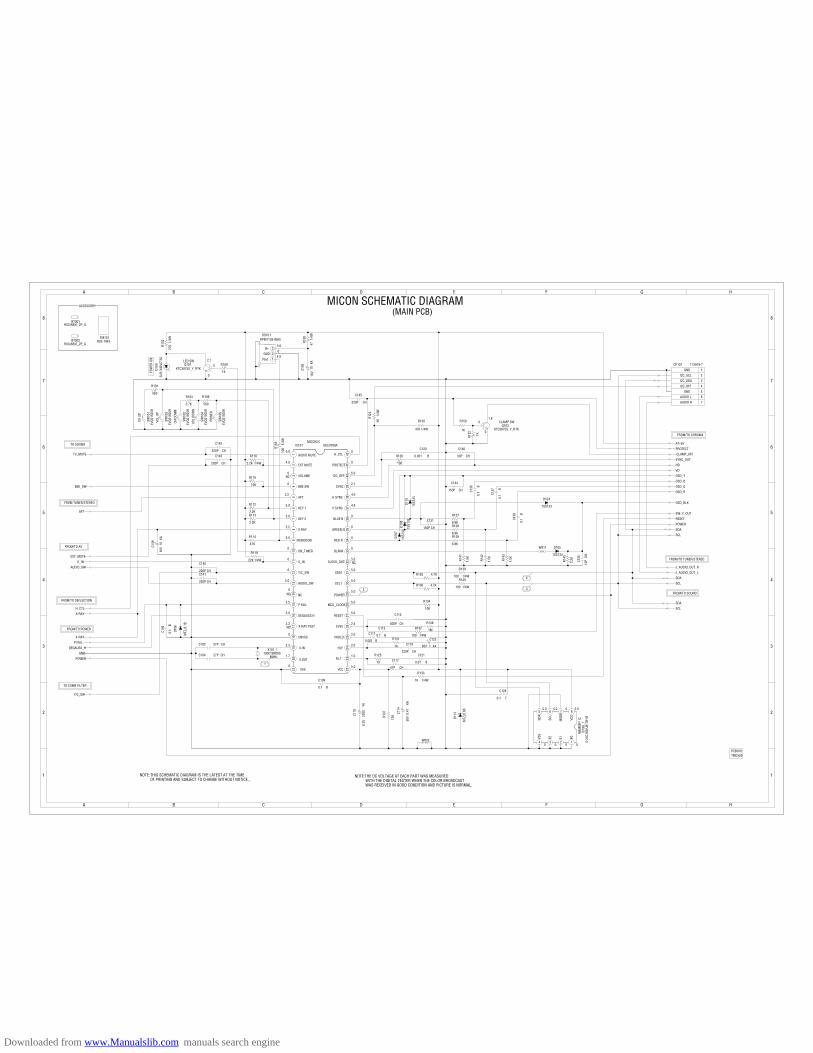
(MAIN PCB)MICON SCHEMATIC DIAGRAM
MCU_CLOCK
CLOCK_CNT
VOLUME
S_IN
X-RAY TEST
4
3
5.0
0
4.92.7
0
0
FROM/TO CHROMA
Y/C_SW
AUDIO_SW
EXT MUTE
P FAIL
RESET
CVIN
VHOLD
HLF
FILT
VCC
SDA
SCL
MOD
E
VCC
VSS
E2 E1 E0
5.005.05.0
0 000
NC
0
0
3.2
0
5.0
FROM/TO AV
FROM/TO POWER
FROM/TO DEFLECTION
FROM/TO TUNER/STEREO
FROM TUNER/STEREO
TO COMB FILTER
1
2
1.80
0
0
5.0
ACCESSORY
FROM/TO SOUND
I2C_SCL
I2C_SDA
I2C_OFF
AUDIO R
AUDIO L
GND
GND
Downloaded from www.Manualslib.com manuals search engine

A B C D E F G H
A B C D E F G H
2
1
3
4
5
6
7
8
2
1
3
4
5
6
7
8
IC601M61283FP R70T
CHROMA IC
1 10 11 12 13 14 15 16
1718
19
2
2021
2223
2425
2627
2829
3
3031
32
33343536373839
4
404142434445464748
49
5
5051
5253
5455
5657
5859
6
6061
6263
64
7 8 9
:SINCE THESE PARTS MARKED BYCAUTIONDESCRIBED IN PARTS LIST ONLYCRITICAL FOR SAFETY,USE ONES
ARE
DANS LA NOMENCLATURE DES PIECESN’UTILISER QUE CELLS DECRITESDANGEREUSES AN POINT DE VUE SECURITE
:LES PIECES REPAREES PAR UN ETANTATTENTION
Q614KTA1504S_Y_RTK
6dBAMP
C615 1
50V
KA
C610 47
16V
YK
C608
4716V YK
C629 10
0016
VYK
C638
1016
VKA
NP
C601
4716V KANP
CAUTION: DIGITAL TRANSISTOR
L601
33uH
R602
12 3W
R649
12 3W
CD802CU274201
OF PRINTING AND SUBJECT TO CHANGE WITHOUT NOTICENOTE:THIS SCHEMATIC DIAGRAM IS THE LATEST AT THE TIME
WAS RECEIVED IN GOOD CONDITION AND PICTURE IS NORMAL.WITH THE DIGITAL TESTER WHEN THE COLOR BROADCAST
NOTE:THE DC VOLTAGE AT EACH PART WAS MEASURED
R647
4.7K
R611
10K
R604
1K
R605
330
R622
6.8K
R625
5.6K
R648
101/
2W
R606 330
R608
3.9K
R613
390
R632 33
K
R618
8.2K
R643
1K
R645
270
R617
100
R616
120 1/2W
R603
330 1/2W
R629
6.8K
R627
100 R628
100
R634
1K
R644
560
R601
15 1/2W
R621
10K
R619
1K
R642
3.3K
R624
15K
R612
10K
R609
100
R607
10K
R641
10K
R654
56K
R651
3.3K
R653
3.3K
R652
3.3K
R635
120K
R636
1.5K
R620
100 R623
100 1/4W R626
100 1/4W
R646
4.7K
R610
100
C625
47P
CH
C633
82P
CH
C604
100P CH
C616
0.01
B
C614
0.1
B
C624
0.1
B
C632
18P
CH
C635
22P
CH
C631
0.01
5B
C636
0.0082 B
C641
0.1 B
C612
0.01
B
C609
0.1
TF
C607
0.01
B
C628
0.01
B
C634
0.1
B
C644 33P CH
C643 33P CH
C637 33P CH
C640
0.01 F
C619
0.1
B
C606
0.33
TF
W81
5
W805
D604
MTZ
J12B
D602
MTZ
J8.2
B
D603
MTZ
J15B
C623
100
16V
YK
C621
150
VKA
C627
150
VKA
C618
150
VKA
C630 0.47
50V
KA
C605 47
16V
YK
C622 47
16V
YK
C611 1
50V
KA
C642
150V KA
C603 47
16V
YK
C645
100
16V
YK
C602 47
16V
YK
D601
1SS1
33
D608
11E1-EIC
D605
1SS1
33D6
06
1SS1
33D6
07
1SS1
33
Q603KTC3875S_Y_RTK
6dB AMP
Q610KTC3875S_Y_RTK
SVM
Q607KTC3203_Y
AT+5V REG
Q606KTC3209_Y
P.CON+5V REG
Q605KTC3875S_Y_RTK
6dB AMP
Q611KTC3209_Y
P.CON 8V REG
Q602KTC3209_Y
P.CON 5V REG
Q604KTC3209_Y
P.CON 5VREG
Q601KTC3209_Y
P.CON 8V REG
Q613KTC3875S_Y_RTK
SVM OFF
X602
100C
T3R5
05
3.57
9545
MHz
CP802AB2013H02-7P
1
2
3
4
5
6
7
VIDEO_IN2
V_IN[YUV]
VIDEO_IN1
U_IN[YUV]
Y_IN[YUV]
VIDEO_IN3
VIDEO_OUT
P.CON+5V
C_V_OUT_SW
P.CON+5VPROTECTY_V_OUT_SW
VIDEO_OUT SW_Y_OUTP.CON+8V[A]
FSC_OUT AT+5V
RESET
POWER
SCL
SDA
TUNER_VIDEO
TUNER+5V
P.CON+8V[B] OSD_BLKP.CON+5V
OSD_R
OSD_G
OSD_B
P.CON+8V[B] VD
P.CON+5VHD
SYNC_OUT
OSD_Y
CLAMP_OFF
UNREG+12V
GND
P.CON+5V
P.CON+8V[A]
GND
V_OUT
EW_OUT
H.OUT
H_SYNC
ABCL
PCB010TMC559
NC
NC
0
0
8.5
7.911.3
8.5
7.9 11.3
NC7.2
7.2
NC
P.CON+8V
4.98.8
5.5HV
CO F
/BDE
F GN
D1
DEF
GND2
FBP
IN
H OU
T
R OU
T
VREG VCC
CVBS4
5.7V VREG OUT
fsc OUT
FAST YUV
DELAYDE Y OUT
EW OUT
VRAMP AGC CAP
V OUT
VRAMP CAP
8.7 VREG OUT
ACL
MONITOR OUT
INV.FBP OUT
V PULSE OUT
B IN
G IN
R IN
FAST BLK
CLK CONT
SDA
SCL
P_CON CONT
MCU CLOCK OUT
MCU RESET
Y SW OUT
15 G OUT
16 B OUT2 AFC FILTER
1 HVCO F/B
48 Y IN(YUV)
C IN(Y/C)
Y IN(Y/C)
LOGI
C GN
D
34 XTAL 3.58
33 V/C GND
CVBS
1
U IN
(YUV
)
CVBS
2
V/C
VCC
CVBS
3
MCU
5.7
VRE
G OU
T
C_AP
C
NC
NCV IN
(YUV
)
VIDEO LINE OUT
NC
NC(GND)
NC(G
ND)
NC(G
ND)
NC(G
ND)
NC(G
ND)
47 NC(GND)
NC(V
cc)
DEF
VCC
NC NC(V
cc)
HI V
CC
5.0
5.5
7.25.0
5.0
FROM/TO TUNER/STEREO
NC
2.2
7.87.3
7.3
1.7 2.3
0.7
1.45.3
0
2.2
0
3.0
8.7
1.9
5.7
3.2
0
0
2.8
3.0
3.0
8.7
4.0
4.0
4.0
3.2 4.0 0 0 0 5.5 0 3.8 8.0 8.0 0 8.0 8.0 4.0 4.0 4.0
2.1
4.9
4.9
4.6
2.9
2.9
2.9
4.2
4.9
3.5
3.5
5.0
3.5
5.0
0
3.6
03.202.85.61.901.25.01.901.203.002.7
FROM/TO MICON
FROM/TO AV
FROM/TO COMB FILTER
FROM/TO DEFLECTION
TO SOUND
FROM POWER
GND
R.OUT
G.OUT
B.OUT
CLAMP_OFF
VM COIL
TO CRT/SVM
NC
CHROMA SCHEMATIC DIAGRAM(MAIN PCB)
5.5
3.8
7.9
3.8
5.5
Downloaded from www.Manualslib.com manuals search engine

A B C D E F G H
A B C D E F G H
2
1
3
4
5
6
7
8
2
1
3
4
5
6
7
8
L401
4.7m
H09
09
TP005
X-RAY TEST
TP006
TP003
TP004PROTECTOR TEST
CP801AB2013H02-5P
1
2
3
4
5
B402
W4B
RH3.
5X6X
1.0
B401
W4B
RH3.
5X6X
1.0
B403
W4B
RH3.
5X6X
1.0X
2
B405
W4BRH3.5X6X1.0
CD803CP83035A
R402
68 1/2W
R438
2.7
2W
VR40
11K
V.PO
SI A
DJ
R434
5.6 10W
IS NON POLAR ONE.THE ALUMI ELECTROLYTIC CAPACITOR MARKED NPTHE RESISTOR MARKED F IS FUSE RESISTOR.NOTE:
R414
27K +-1%
R441
15K +-1%
R413
18K
+-1%
R436
18K 1/4W+-1%
R426
4.7K
1/4W
+-1%
CP401B06B-DVS
1
2
3
4
5
6
IC401 LA78040V.OUTPUT IC
1 2 3 4 5 6 7L402_1
ELH5L4113
T401_1ETH14Y47AY
123
45
HS402763WAA0231
GND
ABL
GND
GND
8E8
TERHEA
E27
E12
B+
E180
S
F
AFC
COLHV
FB401 FJN20A002_M
1
10
11
2
3
4
5
6
7
8
9
BGR
1168
109
175
V801A51LVV896X07(O)
Q4052SD2499(LBOEC1)
H.OUT
B_SHORT
:SINCE THESE PARTS MARKED BYCAUTIONDESCRIBED IN PARTS LIST ONLYCRITICAL FOR SAFETY,USE ONES
ARE
DANS LA NOMENCLATURE DES PIECESN’UTILISER QUE CELLS DECRITESDANGEREUSES AN POINT DE VUE SECURITE
:LES PIECES REPAREES PAR UN ETANTATTENTION
C403 22
50V
YK
C408 1000
25V
MHE
C406 1
50V
YK
C409 10
50V
YK
C430 22
100V
YK
R410_1
150 2W
R452_1
330 1W
R439
1K 1W
CD801CU253401
OF PRINTING AND SUBJECT TO CHANGE WITHOUT NOTICENOTE:THIS SCHEMATIC DIAGRAM IS THE LATEST AT THE TIME
WAS RECEIVED IN GOOD CONDITION AND PICTURE IS NORMAL.WITH THE DIGITAL TESTER WHEN THE COLOR BROADCAST
NOTE:THE DC VOLTAGE AT EACH PART WAS MEASURED
R437
11/
2W
R409_1
1K
R443
150K 1/2W
R420
2.7
1/2W
R417
39K
R415
820
R430
82K
1/2W
R427
680
1/2W
R418
560
1/2W
R406
470
1/2W
R401
4.7K
R407
1.2K
R428
100
1/4W
R453
10K
R432
8.2K 1/2W
R429
1K1/
2W
R433
1K1/
2W
R421
1K1/
2W
R422
560
1/2W
R416
3.3
1/2W
R403 1K
R404
100
C427
0.1100V MMTS
C415_1
33P500V SL
C416
100P
CH
C420
_1 0.01
31.
25KV
CMPP
C418
0.39
250V
PMS
C405
560P
CH
C402
0.01
100V
MM
TS
C417
0.22
100V
MM
TS
C411
0.001 CH
C439
0.00
1B
C425
0.0012KV R
W860
W844
W81
3
W82
1
W861
W85
0D4
10
MTZ
J30B
D403
MTZ
J30B
D404
MTZ
J5.1
B
D406
MTZ
J5.6
B
C410
2.2250V
YK
C426 22
250V
MHEC4
13_1
1000
35V
YK
C407 10
035
VYK
D407
AU02
A-B-
EIC
D415
11E1-EIC
D405
AU02A-EIC
D414
11E1-EIC
D402
11E1
-EIC
D411
AU02A-EIC
Q402KTC3227_Y
H.DRIVE
VD2
V_OUT
GND
P.CON+5V
H.OUT
H_SYNC
ABCL
GND
+B
FBT+B
H+B
H_CTL
X-RAY
NC
NC
115
0
0
ANORD
VCC GNDPUMP UP
AMP+
-THERMAL PROTECTION
25.04.0 0 4.02.0 12.0 25.017
NC
NC
1
2
3
4
5
6
31 2(CP805)
NC
NC
HEATER
180V
NC
NC
GND
21
00.1
19
00.4
17.3
16
FROM/TO POWER
18
TO CRT/SVM
TO CRT/SVM
FROM MICON
SCREEN
FORCUS
FROM/TO CRT
20
026.3 0.1
0108.0
105.0
0
0.2
2.0
0.1
0
8.1
PCB010TMC559
FROM/TO DY
DEFLECTION SCHEMATIC DIAGRAM(MAIN PCB)
FROM/TO CHROMA
17.3
115
180
FROM/TO MICON
Downloaded from www.Manualslib.com manuals search engine

A B C D E F G H
A B C D E F G H
2
1
3
4
5
6
7
8
2
1
3
4
5
6
7
8
HS501763WAA0244
CP502A1561WV2-2P
1
2
6.3A 125V
6.3A 125V
BLAD
EW
IDE
BLACK
WHITE
21
CD501_10R615901
AC120V_60Hz
IS THE LIVE CONNECTIONCAUTION:
L5011R5A123F28Y
COIL,LINE FILTER
1 2
3 4CP501A3963WV2-3PD
12
21
L5038R200024
DEGAUSS COIL
RY501ALKS321
12
3 4
FH502EYF-52BCY
FH501EYF-52BCY
F501
6.3A125V
6.3A125Vor51MS063L
IC504LTV-817M-VB
FEED BACK
12 3
4
TH501_2
B59203-S1060-B14
CP507003P-2100
1
CP508003P-2100
1
N’UTILISER QUE DES FUSIBLE DE MEME TYPE
CAUTIONREPLACE ONLY WITH THE SAME TYPE FUSE
:FOR CONTINUED PROTECTION AGAINST FIRE HAZARD,
:POUR UNE PROTECTION CONTINUE LES RISQUES D’INCEIEATTENTION
S
DG
Q5022SK3326(2)
SWITCHING
T501 8140066S
1
10
11
12
13
14
15
16
2
3
5
6
7
8 9
CP851AB2013H02-4P
1
2
3
4
B501
BL02RN1-R62
B504
W5RH3.5X5X1.0
R541_1
0.22 1W
VR50
222
K
+B A
DJ
R501
1 7W
IS NON POLAR ONE.THE ALUMI ELECTROLYTIC CAPACITOR MARKED NPTHE RESISTOR MARKED F IS FUSE RESISTOR.NOTE: :SINCE THESE PARTS MARKED BYCAUTION
DESCRIBED IN PARTS LIST ONLYCRITICAL FOR SAFETY,USE ONES
ARE
DANS LA NOMENCLATURE DES PIECESN’UTILISER QUE CELLS DECRITESDANGEREUSES AN POINT DE VUE SECURITE
:LES PIECES REPAREES PAR UN ETANTATTENTION
Q5032SA1371
+B SW.
Q508KTA1271_Y
P.CON+12V SW.
Q5122SA1624
CURRENT DET.
C509 47
25V
YK
C527 2200
16V
YKC5
21 220
160V
YXF
C504 2.2
50V
YK
C507
470
200V
UP
R542
0.15 1W
R517_1
0.22 3W
R527
0.68 2W
R502
330 2W
CD851CU244201
OF PRINTING AND SUBJECT TO CHANGE WITHOUT NOTICENOTE:THIS SCHEMATIC DIAGRAM IS THE LATEST AT THE TIME
WAS RECEIVED IN GOOD CONDITION AND PICTURE IS NORMAL.WITH THE DIGITAL TESTER WHEN THE COLOR BROADCAST
NOTE:THE DC VOLTAGE AT EACH PART WAS MEASURED
R535
3.9K
1/4W
R510
100 1/4W
R520
1.5M
1/2W
R500
2.7M
1/2W
+-10
%
R553
6.8K
1/2W
R540
1.2M 1/4W
R539
1.2M 1/
4W
R516
10K
R543
1K1/
4W
R508
100 1/4W
R512
1K1/
2W
R511
22K
R545
150 1/4W
R533
270
R554
100K
1/2W
R506
6.8K
1/4W
R513
10K
R505
10K
1/4W
R507
82K
1/4W
R547
100
1/4W
R536
47K 1/4W
R525
15K
R524
3.3K 1/4W
R515
10K 1/4W
R546
1001/4W
R532
1.5K
R503
10K 1/4W
R544
270 1/4W
R519
10K
R537
33K 1/4W
C513
_1
0.00
125
0VKX
C519
_1
0.00
125
0VKX
C505
_1
0.22
275V
ECQU
L
C511
220P
CH
C541
0.05
6B
C520
0.001500V B
C508
_1
0.00
2225
0VKX
C554
0.022 B
C535
0.00
12K
VR
C517
0.00152KV R
C506
_1 0.1
275V
ECQU
L
C512
0.047100V MMTS
C524 0.00
150
0VB
C502
0.0012KV
R
C503
0.0012KV
R
W81
7
W801
W825
W806
D528
MTZ
J5.6
B
D509
MTZJ18B
D523
MTZ
J18B
D525
MTZ
J12B
D508
MTZ
J3.9
B
C539_1
4.7100V YK
C550
100016V YK
C501
1000
25V
YK
D506
1N4937
D512
21DQ09N
D524
1SS133
D507
1SS133
D514
1SS1
33
D505
30DF6-FC
D510
FE201-6L49
D513
1SS1
33
D516
1SS133
D511
1N4937
D520
1SS1
33
D517
1SS133
D504
RM11
C-EI
C
D501
RM11
C-EI
C
D502
RM11
C-EI
C
D503
RM11
C-EI
C
Q514KTC3203_Y
SWITCHING
Q5052SC2909
STAND BY SW.
Q509KTC3198
STAND BY SW.
Q507KTC3198
FEED BACKSWITCHING
Q504KTC3198
RELAY DRIVE
SOUND+B
P.CON+12V
GND
SOUND_GND
H+B
+B
FBT+B
GND
P.CON+B
GND
UNREG+12V
GND
P.FAIL
X-RAY
DEGAUSS_H
POWER
GND
GND1
P.CON+12V
GND
GND
NC
NC
115.7
38
6.3A 125V(F501)
6.3A 125V(F501)
25.0141.6
40.0 240.0
26.0
138.9
50.0
9.7
10.7
1.5
16.3
159.4
0
00
P1
P2 00
114.7
115.5
115.2
115.1
TO CRT5.7
6.39.7
115.4
WHITE
BLACK
10.9
00
P.CON+12V
GND
NC
P.CON+B
NC
PCB010TMC559
12.9 12.9
12.8
0.80.7
0
5.305.3
TO SOUND
FROM/TO DEFLECTION
TO TUNER/STEREO
TO CHROMA
FROM/TO MICON
TO AV
POWER SCHEMATIC DIAGRAM(MAIN PCB)
FROM/TO COMB FILTER
0
1.5
159.4
Downloaded from www.Manualslib.com manuals search engine

A B C D E F G H
A B C D E F G H
2
1
3
4
5
6
7
8
2
1
3
4
5
6
7
8
IC1001 AN17808BSOUND AMP IC
1 10 11 122 3 4 5 6 7 8 9
Q1001KRC111SRTK
MUTE
CP1001A2502WV2-4P
1
2
3
4
IC30
1NJ
M21
50AM
BBE
IC
1 10
111213141516171819
2
20
3 4 5 6 7 8 9
SPEAKER
SP1002SG05K07BRA
SPEAKER
SP1001SG05K07BRA
J1001MSJ-2000_AG
HEADPHONE JACK
1
2
3
4
5
6
7
4
3
2
1
CD1001
CU14411A
IC30
2AN
5891
SA-E
1V
TONE
CON
TROL
IC
1 10 11 12 13 14 15 16
171819
2
20212223242526272829
3
303132
4 5 6 7 8 9
HS1001763WAA0215
L301
100uH 0305
:SINCE THESE PARTS MARKED BYCAUTIONDESCRIBED IN PARTS LIST ONLYCRITICAL FOR SAFETY,USE ONES
ARE
DANS LA NOMENCLATURE DES PIECESN’UTILISER QUE CELLS DECRITESDANGEREUSES AN POINT DE VUE SECURITE
:LES PIECES REPAREES PAR UN ETANTATTENTION
C101
1_1
330
25V
YK
C100
7
2250
VYK
C100
3
1000
25V
YK
C100
9
1000
25V
YK
C100
4
1000
25V
YK
C1001_1
150V KA
C1002_1
150V KA
C328 10
50V
YKC3
30 100
16V
YK
C305
1050
VYK
C321
1050
VYK
C100
8
0.22
50V
YK
OF PRINTING AND SUBJECT TO CHANGE WITHOUT NOTICENOTE:THIS SCHEMATIC DIAGRAM IS THE LATEST AT THE TIME
WAS RECEIVED IN GOOD CONDITION AND PICTURE IS NORMAL.WITH THE DIGITAL TESTER WHEN THE COLOR BROADCAST
NOTE:THE DC VOLTAGE AT EACH PART WAS MEASURED
R310
10K
R306
20K
R308
20K
R312
10K
R305
20K
R307
20K
R309
10K
R313
1K 1/4W
R1002
270 1/2WR1001
270 1/2W
R1009
68K 1/4W
R314
220K
R311
10K
R101
1
10K
R1004
22K
R1003
22K
R1013
10K
R303
100 1/4W
R304
100 1/4W
R101
0
10K
R302
2.7K 1/4WR301
2.7K 1/4W
C320
56P
CHC3
22
56P
CH
C326
0.033 B
C324
0.0033 B
C323
0.0033B
C325
0.033B
C301
0.03
3B
C312
0.01
B
C100
5
220P
B
C334
1B
C311 0.1
B
C315
0.1
B
C303
0.01
B
C310
0.03
3B
C313
0.01
B
C307
0.01
5B
C309
0.039B
C101
2
0.00
47B
C101
0
0.00
47B
W803
W858
W83
5
C329
1016
VKA
C327
1016
VKA
C332 10
16V
KA
C333 10
50V
YK
C308
1050
VYK C3
16 1050
VYK
C306
100
16V
YK
C302 10
50V
YK
C319 10
50V
YK
C318
1050
VYK
C314
1050
VYK
C317 10
50V
YK
C304
1050
VYK
CAUTION: DIGITAL TRANSISTOR
SW_AUDIO_L
SW_AUDIO_R
P.CON+8V[B]
GND
SDA
SCL
BBE_SW
VOLUME
TV_MUTE
SOUND+B
GND
P.CON+12V
SOUND_GND
PCB010TMC559
(L)
8 OHM 5W
8 OHM 5W
(R)
2.5W
2.5W
4.84.84.84.84.84.8
8.9
4.8
4.84.84.84.84.84.84.8 0 8.9
BBE
09.54.8
8.9
NC
RIPPLEFILTER
+
-+
NC
-+
+ATT.
VCCGND STAND-BY OUTMUTEOUT
CH2 CH1GND CH2ININ
CH1RF VOL
VOLATT.CONT.
0
03.6
controlMODE
R IN VrefVCC
PF1 AGC L IN
SURRAGC +
L ONTVDBDLBLTGNDPF4PF3PF2NCNC
SCLSDAR OUT
NC NC
NCTDBLD
Balance/MUTEControl
Volume 2.2K
+
+
RTRBBBNCNC
Tone
Control
NC
27
26
3.9 1.7 3.0 0 3.9 3.9 3.9 0 4.0 4.0 0 0 2.0 2.9 4.0
2.3 7.9 4.5 4.0 0 0 4.0 4.0 4.4 3.0 2.0 0 0 4.0 3.5 3.5
0 0.2 16.0 0 0.2 0.7 0 16.5 12.73.7
SOUND SCHEMATIC DIAGRAM(MAIN PCB)
FROM TUNER/STEREO
FROM CHROMA
FROM/TO COMBI FILTER
FROM/TO MICON
FROM POWER
NC NC NC NC
NCNCNC NC0
22
23
25 24
0.70
(2.5
MM
)
Downloaded from www.Manualslib.com manuals search engine

A B C D E F G H
A B C D E F G H
2
1
3
4
5
6
7
8
2
1
3
4
5
6
7
8
IC90
2AN
5829
SSO
UND
DECO
RDER
IC
1 10 11 12
13141516171819
2
2021222324
3 4 5 6 7 8 9
TU001 115-V-K015AR_B
1 10 11 12 13 14 15 16 17
18
19
2
20
21
3 4 5 6 7 8 9
L901
100uH 0305
:SINCE THESE PARTS MARKED BYCAUTIONDESCRIBED IN PARTS LIST ONLYCRITICAL FOR SAFETY,USE ONES
ARE
DANS LA NOMENCLATURE DES PIECESN’UTILISER QUE CELLS DECRITESDANGEREUSES AN POINT DE VUE SECURITE
:LES PIECES REPAREES PAR UN ETANTATTENTION
Q902KTA1504S_Y_RTK
BUFFER
Q901KTA1504S_Y_RTK
BUFFER
C903 4.7
50V
KA
C910 0.33
50V
KA
C914 3.
350
VKA
C904 4.7
50V
KAC9
05 4.7
50V
KAC9
07 1050
VYK
C001
_1 100
6.3V
YK
C916
100
10V
YK
OF PRINTING AND SUBJECT TO CHANGE WITHOUT NOTICENOTE:THIS SCHEMATIC DIAGRAM IS THE LATEST AT THE TIME
WAS RECEIVED IN GOOD CONDITION AND PICTURE IS NORMAL.WITH THE DIGITAL TESTER WHEN THE COLOR BROADCAST
NOTE:THE DC VOLTAGE AT EACH PART WAS MEASURED
R907
220K
R906
39K
R901
220
1/4W
R902
56K
1/4W
R903
39K
R912
330
R006
100
R001
68K 1/2WR002
68K 1/2W
R904
220
1/4W
R905
56K
1/4W
C912
0.02
2B
C908
0.02
2B
C911
0.04
7B
C913
0.1
B
C917
0.1
B
C915
0.1
BC9
18
0.1
BC0
05
0.1
F
C002
0.1
B
W82
0
W81
9
W82
9
W83
0
W812
D001
MTZ
J33B
C902
150V KA
C901
150V KA
C919 10
50V
YK
TUNER+5V
TUNER_VIDEO
P.CON+8V[B]
P.CON+5V
P.CON+B
GND
AFT
SCL
SDA
J_AUDIO_OUT_L
J_AUDIO_OUT_R
SW_AUDIO_L
SW_AUDIO_R
J_AUDIO_OUT_L
J_AUDIO_OUT_R
AUDIO_IN1/2[R]
AUDIO_IN1/2[L]
AUDIO_IN3[R]
AUDIO_IN3[L]
PCB010TMC559
NC NC
2.3 NoiseDet
SpectralRMS Det
SAPFilter
NoiseFilter
SpectralFilter
SAPDet
StereoFilter
GND
InputVCA
PilotDetSt.PLL
CancelPilot
SpectralExpanddbx De-Emph
SAPDemod
Wide BandRMS Det
Wide BandFilter
L+R Filter L+R Demod
IIC Decoder
L-R DemodL-R Filter
fH.2fH Trap Filter
ZAPOUT SW
Matrix
OffsetCancel
OffsetCancel
Wide BandExpand
DAC
(L-R)/SAPSwitch
De-Emph75us
SAPoutFilter
0 2.3 2.3 2.2 2.2 0.4
Vcc
5.1 2.4 2.4 0.4 2.3 3.4
2.3 2.3 2.3 2.3 0 5.0 5.0 0 3.7 3.6 2.6 3.7
AGC
NC NC NC
MB
MB
VIDE
OOU
T
IF O
UT
BTSIF
OUT
AUDI
OOU
T
AFT
SDA
SCL
(ADR
ESS)
(X’T
AL)
2.3
0
3.2
3.2
2.3
0
NC NC NCNCNC
TUNER/STEREO SCHEMATIC DIAGRAM(MAIN PCB)
FROM/TO MICON
TO SOUND
FROM/TO AV
FROM/TO CHROMA
FROM POWER
TO MICON
NC
Downloaded from www.Manualslib.com manuals search engine

A B C D E F G H
A B C D E F G H
2
1
3
4
5
6
7
8
2
1
3
4
5
6
7
8
J702YKF51-5503
S-JACK
12
34
56
HNC E
J707HTJ-032-03AR
FRONT-AUDIO.R
123
HNC E
J705HTJ-032-03AY
FRONT-VIDEO
123
HNC E
J706HTJ-032-03AW
FRONT-AUDIO.L
123
H1H1
H2
EE
J704MSP-213V1-652_NI
YUV_IN(REAR)
123
45
EEH1
NCH1
H2
J701MSP-213V2-432_NI
LINE1(REAR)
123
4
56
EEH1
NCH1
H2
J703MSP-213V2-432_NI
LINE2(REAR)
123
4
56
EEH1
NCH1
H2
J708MSP-213V2-432_NI
A/V_OUT(REAR)
123
4
56
IC701 MM1501XNREAUDIO SW(R) IC
12
3 45
6
IC702 MM1501XNRE
AUDIO SW(L) IC
12
3 45
6
Q709KTA1504S_Y_RTK
BUFFER
C708
100
16V
YK
C702
1016V KAC701
1016V KA
C710
4716V KANP
OF PRINTING AND SUBJECT TO CHANGE WITHOUT NOTICENOTE:THIS SCHEMATIC DIAGRAM IS THE LATEST AT THE TIME
WAS RECEIVED IN GOOD CONDITION AND PICTURE IS NORMAL.WITH THE DIGITAL TESTER WHEN THE COLOR BROADCAST
NOTE:THE DC VOLTAGE AT EACH PART WAS MEASURED
R701
22 1/4W
R703
2.2K
R702
22 1/4W
R729 75
R726
1K
R733
1K
R727 75
R734
1K R728
1K
R739 75
R705
3.3K
R706
3.3K
R709
270
R725 75 R736 75R730 75
R708
1K
R724 75
R711
1KR710
1K 1/4W
R704
1K
R735 75
R721
68
R745
1K
R746
1K
C736
0.00
56B
C738
0.00
56B
C725
1 B C722
1 B
C735
0.00
56B
C737
0.00
56B
C727
1 B C724
1 B
C734
0.1 B
C706 0.1
F
C741
0.00
56B
C742
0.00
56B
C719
1 B
C720
1 B
D703
MTZ
J12B
D702
MTZ
J12B
D705
MTZ
J12B
D704
MTZ
J12B
D701
MTZ
J12B
D706
MTZ
J12B
D709
MTZ
J6.2
B
C728
47016V YK
C733
2216V KA
C705 22
016
VYK
C707
1016V KA
C711
1016V KA
Q711KTC3875S_Y_RTK
MUTE
Q712KTC3875S_Y_RTK
MUTE
V_IN[YUV]
U_IN[YUV]
Y_IN[YUV]
VIDEO_OUT
VIDEO_IN2
VIDEO_IN1
VIDEO_IN3
J_AUDIO_OUT_R
J_AUDIO_OUT_L
AUDIO_IN1/2[R]
AUDIO_IN1/2[L]
AUDIO_IN3[L]
AUDIO_IN3[R]
EXT_MUTE
AUDIO_SW
S_IN
S_VIDEO_IN[Y]
S_VIDEO_IN[C]
LINE3_A_IN_L
LINE3_A_IN_R
P.CON+12V
GND
SW1
V.OUT
Vcc Vin2
Vin1
GND
SW1
V.OUT
Vcc Vin2
Vin1
GND
FROM/TO MICON
FROM/TO TUNER/STEREO
FROM/TO CHROMA
0
5.20
29
28
0
0
3.7
12.7
0
3.7
12.7
4.5
0
4.5
4.5
0
4.5
PCB010TMC559
4.6
FROM POWER
TO COMB FILTER
0.1
AV SCHEMATIC DIAGRAM(MAIN PCB)
0.2
0.1
0.2
Downloaded from www.Manualslib.com manuals search engine
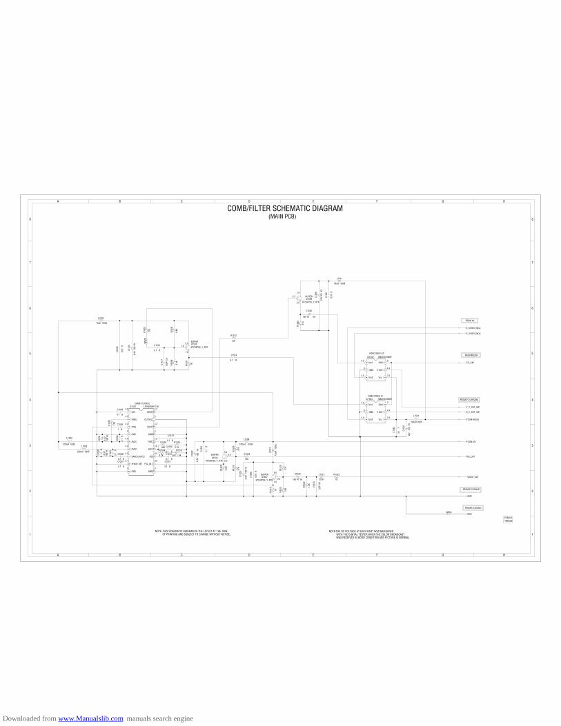
A B C D E F G H
A B C D E F G H
2
1
3
4
5
6
7
8
2
1
3
4
5
6
7
8
IC1501 LA76605M-TLMCOMB FILTER IC
1
1011
1213
1415
1617
18
23
45
67
89
IC1503 MM1501XNREVIDEO SW(C) IC
12
345
6
IC1502 MM1501XNRE
VIDEO SW(Y) IC
12
345
6
L1503
220uH 0305
L1502
220uH 0305
L1501
100uH 0305
C153
2
100
16V
YK
L1511
15uH 0305
L1505
15uH 0305
L1508
100uH 0305
L151
0
15uH
0305
L1512
22uH
OF PRINTING AND SUBJECT TO CHANGE WITHOUT NOTICENOTE:THIS SCHEMATIC DIAGRAM IS THE LATEST AT THE TIME
WAS RECEIVED IN GOOD CONDITION AND PICTURE IS NORMAL.WITH THE DIGITAL TESTER WHEN THE COLOR BROADCAST
NOTE:THE DC VOLTAGE AT EACH PART WAS MEASURED
R150
7
1K
R1512
470
R153
0
470
R150
6
3.3K
R150
3
270
R150
5
6.8K
R150
2
100
R1529
2.7K
R1528
82KR1504
8.2K
R150
9
47K
R150
8
3.9K
R151
0
47K
R1523
100
R151
8
27K
R151
6
1K
R151
9
24K
R1522
1K
R152
0
1.2K
C152
1
0.1
B
C150
9
0.01
B C1513
0.1 B
C151
7
100P
CH
C1519
0.1 B
C153
1
0.01
B
C1504
0.1 B
C1505
1 B
C150
8
0.1
B
C1515
0.1 B
C1514
0.1 B
C1516
0.1 BC1512
0.1 B
C1506
0.1 BC1507
0.1 B
C150
3
0.1
B
C152
6
0.01
B
C153
3
22P
CH
C152
3
0.1
F
W804
W84
8
C151
0
100
6.3V
YK
C152
8
100
16V
YK
C150
1
100
6.3V
YK
C150
2
1006.3V YK
C1518
150V KA C152
0
100
6.3V
YK
C152
5 100
6.3V
YK
C1530
4716V YK
C1535
1016V KA
Q1508KTC3875S_Y_RTK
BUFFER
Q1503KTC3875S_Y_RTK
BUFFER
Q1504KTC3875S_Y_RTK
BUFFER
Q1507KTC3875S_Y_RTK
BUFFER
S_VIDEO_IN[C]
S_VIDEO_IN[Y]
Y/C_SW
Y_V_OUT_SW
C_V_OUT_SW
P.CON+8V[A]
P.CON+5V
FSC_OUT
VIDEO_OUT
GND
GND
PCB010TMC559
FROM/TO SOUND
FROM/TO POWER
COMB/FILTER SCHEMATIC DIAGRAM
2.5
2.0
5.01.0
1.0
CIN
INSEL
YIN2
AVCC
DVCC
SAND CASTLE
PHASE DET FSC_IN
YIN1
AFC
RD
YOUT
OUTSEL
COUT
GND
GND GND
GND
2.6
4.9
4.2
0
4.9
4.9
4.0
2.1
0
2.4
0
3.4
0
2.9
3.6
9.5
0.9
0
2.45.0
2.0
(MAIN PCB)
5.0
2.21.6
SW1
V.OUT
VccVin2
Vin1
GND
SW1Vin1
GND V.OUT
Vin2 Vcc
4.5
0
4.5
4.5
0
4.5
0
4.4
7.9
0
4.4
7.9
FROM MICON
FROM AV
FROM/TO CHROMA
7.9
Downloaded from www.Manualslib.com manuals search engine

A B C D E F G H
A B C D E F G H
2
1
3
4
5
6
7
8
2
1
3
4
5
6
7
8
CP80
400
5P-2
100
1
R.SIGNALG.SIGNALB.SIGNAL
F
J801CVT3275-5101
1
10
11
4
5
6 7 89
CP852A2001WV2-3P
1
2
3
CP80
3A2
361W
V2-3
P
123
S852
S851
CP852BB2013H02-3P
1
2
3
HS851763WSA0018
CP851BA2001WV2-4P
1
2
3
4
L803
150u
H
L804
150u
H
L802
150u
H
TP805
TP806
TP804
CP80
1BA2
001W
V2-5
P
12345
B851
W5R
H3.5
X5X1
.0
B852
W5R
H3.5
X5X1
.0
B853
W5RH3.5X5X1.0
CD852_1CU232001
R855
270 1/2W
:SINCE THESE PARTS MARKED BYCAUTIONDESCRIBED IN PARTS LIST ONLYCRITICAL FOR SAFETY,USE ONES
ARE
DANS LA NOMENCLATURE DES PIECESN’UTILISER QUE CELLS DECRITESDANGEREUSES AN POINT DE VUE SECURITE
:LES PIECES REPAREES PAR UN ETANTATTENTION
Q8582SA1837
SWITCHING
Q857KTA1266
SWTCHING
C863
_1
4716
VYK
C862
_1
4716
VYK
C864 10
160V
YK
C854
1016
0VYK
R881
150 2W
R806
15K
2W
R808
15K
2W
R804
15K
2W
OF PRINTING AND SUBJECT TO CHANGE WITHOUT NOTICENOTE:THIS SCHEMATIC DIAGRAM IS THE LATEST AT THE TIME
WAS RECEIVED IN GOOD CONDITION AND PICTURE IS NORMAL.WITH THE DIGITAL TESTER WHEN THE COLOR BROADCAST
NOTE:THE DC VOLTAGE AT EACH PART WAS MEASURED
R872
1.2K
1/4W
R854
33K 1/4W
R853
22K
1/4W
R821
330
1/4W
R822
220
1/4W
R820
220
1/4W
R866
2.2K
1/4W
R873
68K
1/4W
R875
1.2K
1/4W
R878
681/
2W
R876
12K 1/4W
R874
68K1
/4W
R871
1.5K
1/4W
R868
821/4W
R869
82 1/4W
R864
39K
1/4W
R830
2.7K 1/4W
R856
1K1/
4W
R859
2.7K
1/4W
R861
33K 1/4W
R860
331/
4W
R857
470
1/2W
R858
100 1/4W
R863
3.9K1/4W
R862
3.9K
1/4W
R865
56K
1/4W
R870
1.5K
1/4W
R877
681/
2W
R867
101/
2W
R879
2.7
1/2W
R880
2.7
1/2W
R828
2.7K 1/4W
R829
2.7K 1/4W
R813
220 1/4W
R814
220 1/4W
R809
100
1/4W
R811
2.2K 1/4W
R812
2.2K 1/4W
R815
220 1/4W
R819
330
1/4W
R818
220
1/4W
R817
330
1/4W
R810
2.2K 1/4W
C821_1
100P CH
C806
680P
CH
C805
390P
CH
C8610.0047500V B
C859
100P
CH
C856
0.01
B
C855
560P
CH
C857
0.001 B
C858
100P
CH
C860
0.0047500V B
C865
150P500V BC808
0.00222KV B
C813
0.00
22M
C804
470P
CH
W810
W80
2
W805
W809
W807
W808W820
W811
W806
W804
C853 47
16V
YK
C809
1250V YKC8
52 4716
VYK
D853
1SS1
33
D854
1SS1
33
D858
10EL
S2N
D857
10EL
S2N
D856
1SS1
33
D852
1SS133
D855
1SS1
33
D801
1SS133
D807
1SS133
D802
1SS133
D803
1SS133
D804
1SS133
D805
1SS133
D806
1SS133
D809
1SS133
D808
1SS133
Q855KTC3198
SWITCHING
Q8592SC4793
SWTCHING
Q856KTC3198
SWTCHING
Q852KTC3198
AMP
Q854KTC3198
BUFFER
Q8532SC752(G)(TM)_Y
AMP
Q801KTC4217
RED AMP
Q810KTC3199_Y
RED AMP
Q802KTC4217
GREEN AMP
Q811KTC3199_Y
GREEN AMP
Q803KTC4217
BLUE AMP
Q812KTC3199_Y
BLUE AMP
CP802BA2001WV2-7P
1
2
3
4
5
6
7
5.7
NCNC
NC
NC NC
39
PCB110
1
2
3
1
2
3
PCB060
TCA391
TEAA93
VM1
VM2
FROM/TO VM
11.8
2.5
54.5
1.02.0
108.054.5
110.0
11.8
2.51.8
1.8
02.0
38
0 6.2
0
0
121.0
0
119.0
117.0582.0
FOCU
S
CRT BLOCK
1.9
11.8
5.7
00
CRT/SVM SCHEMATIC DIAGRAM
119.7
7.37.8
7.87.3
123.9
FROM
DEF
LECT
ION
SVM BLOCK
6.0
GND
P.CON+12V
NC
P.CON+B
FROM POWER
NC
10.3
0.12.0
180VNCGND
HEAT
ER
NC GND
GND
GND
SCRE
EN
P.CON+8V
GND(SIGNAL)
R.OUT
G.OUT
B.OUT
CLAMP_OFF
VM COIL
FROM CHROMA
37
123.5
7.37.8
3.0
2.4
7.3
7.3
2.4
3.0
3.17.3
TO VM COIL
2.5
(CP852B)
FROM/TO CRT/SVM
(CP852)
(CP851A)
(CP802A)
(CP8
01A)
(CD8
03)
(CRT PCB)
(VM COIL PCB)
Downloaded from www.Manualslib.com manuals search engine

H-1
1ms
5.0V
26
WAVEFORMS
1
2
3
17
16
MICON
18
50µs
1.0V
100µs
1.0V
5µs
1.0V
5ms
200mV
5ms
5.0V
5ms
10V
22
1ms
50mV
1ms
200mV
23
1ms
100mV
24
1ms
100mV
254
50µs
1.0V
20µs
50V
19
20µs
2.0V
20
21
20µs
200V
The following waveforms were measured at the point of the correspondingballoon number in the schematic diagram.
NOTE:
DEFLECTION
SOUND
Downloaded from www.Manualslib.com manuals search engine

H-2
1ms
5.0V
27
20µs
200mV
29
20µs
50V
37
20µs
200mV
28
20µs
50V
38
20µs
50V
39
WAVEFORMS
The following waveforms were measured at the point of the correspondingballoon number in the schematic diagram.
NOTE:
AV
CRT/SVM
Downloaded from www.Manualslib.com manuals search engine

MECHANICAL EXPLODED VIEW
I-1
202
202
202
202
202
202
102A
202
204
102
104
102B
102B
107
207
206
206
205
207
113
PCB010(MAIN PCB ASS'Y)
205
101A
101B
101D
106
101
115
114
112
203
111
108
203111
202
202
112
101C
101E101G
101F
204101G
101H
101I
101I 203
111
108
203111
202
202
112
112
201
201
201
201103
105 PCB060(VM COIL PCB ASS'Y)
PCB110(CRT PCB ASS'Y)
206
109
109
110
110
Downloaded from www.Manualslib.com manuals search engine

MECHANICAL EXPLODED VIEW(PACKING DIAGRAM)
I-2
122, 123, 124, 125, TM101
120
118
119
117
116
118
119
Downloaded from www.Manualslib.com manuals search engine

MECHANICAL REPLACEMENT PARTS LIST
Location No. TSB P/N Reference No. Description
101 AE003196 A3M7110720 CABINET,FRONT ASSY101A AE003197 701WPJC568 CABINET,FRONT101B AD302006 711WPA0184 PLATE,FRONT101C AD302007 713WPA0263 GLASS,LED101D AD302008 7235490036 BADGE,BRAND101E AD302009 735WPA0728 STOPPER,BUTTON 1101F AD302010 735WPA0732 STOPPER,BUTTON2101G AE003198 735WPBB006 BUTTON,FRAME101H AE003199 735WPJA822 BUTTON,POWER101I AE000003 800WQ00045 FELT SHEET
102 AE003200 A3M7110740 CABINET,BACK ASSY102A AE003201 702WPAA598 CABINET,BACK102B AE003072 800WQ0A045 FELT SHEET
103 AD300759 741WUA0021 SPRING,EARTH104 AE004063 722549A349 SHEET,RATING105 AE004064 723000C287 POP LABEL106 AD300132 7230006818 SHEET,CAUTION107 AE000008 7260000345 SHEET,SERVICEMAN108 AD302015 761WPA0220 HOLDER,SPEAKER109 BZ710259 762WPA0011 HOLDER,CRT WIRE
110 AE001107 800WR0A026 SHEET,CRT SUPPORT (D)111 AD300518 801WR00001 DAMPER,SPEAKER112 AD300519 82A40B0104 FLAT WASHER113 BZ710260 899HV3T000 HOLDER,ANODE WIRE114 AE000007 7220001107 SHEET,HWC115 AE000006 7220001119 SHEET,CSA WARNING116 AE003204 723000C491 SHEET,BAR CODE117 AE000010 791WHA0085 LAMIFILM,BAG118 AD302017 792WHA0432 PACKAGE,TOP119 AD302018 792WHA0433 PACKAGE,BOTTOM
120 AE003205 793WCDC089 GIFT BOX121 AE003076 A3M7110975 INSTRUCTION BOOK KIT122 AD301213 JA4UD300 POLYBAG,INSTRUCTION(RED CAUTION)123 AD300022 J3I70417 REGISTRATION CARD124 AD300023 J3I70436 ESP CARD125 AE003080 J3M71101A INSTRUCTION BOOK
201 AD302054 8141J50C54 SCREW,TAP TITE(P) GW22 5x35202 BZ710035 8117540A64 SCREW,TAPPING(B0) TRUSS 4x16203 BZ710034 8117140A24 SCREW,TAPPING(B0) PAN 4x12204 BZ710031 8110630A04 SCREW,TAP TITE(P) BRAZIER 3x10205 BZ710018 8107630804 SCREW,TAP TITE(S) BRAZIER 3x8206 BZ710239 8109I30A04 SCREW,TAP TITE(B) WH7 3x10207 BZ710019 8109630802 SCREW,TAP TITE(B) BRAZIER 3x8
J1-1
Downloaded from www.Manualslib.com manuals search engine

ELECTRICAL REPLACEMENT PARTS LIST
Location No. TSB P/N Reference No. DescriptionRESISTORS
! R402 BZ210041 R635U2680J R,FUSE 68 OHM 1/2W ! R410 AD301344 R3X18A151J R,METAL OXIDE 150 OHM 2W ! R416 AD301593 R002T23R3J RC 3.3 OHM 1/2W ! R420 AD301345 R002T22R7J RC 2.7 OHM 1/2W ! R426 BZ210030 R4X5T4472F R,METAL 4.7K OHM 1/4W
R434 AD301972 R5X2CF5R6J R,CEMENT 5.6 OHM 10W ! R436 BZ210023 R4X5T4183F R,METAL 18K OHM 1/4W ! R438 BZ210104 R6558A2R7J R,FUSE 2.7 OHM 2W
R439 AE000676 R3K181102J R,METAL 1K OHM 1W ! R441 AD300037 R4X5T6153F R,METAL 15K OHM 1/6W ! R452 BZ210217 R3X181331J R,METAL OXIDE 330 OHM 1W ! R500 BZ210080 R0G3K2275K RC 2.7M OHM 1/2W ! R501 AD301596 R5X2AE010J R,CEMENT 1 OHM 7W ! R502 AD301016 R3X28A331J R,METAL OXIDE 330 OHM 2W ! R506 BZ210162 R002T4682J RC 6.8K OHM 1/4W ! R517 AD301973 R3X28BR22J R,METAL 0.22 OHM 3W ! R520 BZ210206 R002T2155J RC 1.5M OHM 1/2W ! R527 BZ210149 R3X18AR68J R,METAL OXIDE 0.68 OHM 2W ! R541 BZ210190 R63581R22J R,FUSE 0.22 OHM 1W ! R542 AD301017 R3X181R15J R,METAL OXIDE 0.15 OHM 1W ! R602 AD301975 R3X28B120J R,METAL OXIDE 12 OHM 3W
R649 AD301975 R3X28B120J R,METAL OXIDE 12 OHM 3W ! R804 BZ210026 R3X18A153J R,METAL OXIDE 15K OHM 2W ! R806 BZ210026 R3X18A153J R,METAL OXIDE 15K OHM 2W ! R808 BZ210026 R3X18A153J R,METAL OXIDE 15K OHM 2W ! R855 AD301976 R65582271J R,FUSE 270 OHM 1/2W ! R881 AD301344 R3X18A151J R,METAL OXIDE 150 OHM 2W
CAPACITORSC408 BZ110032 E5EZF3102M CE 1000 UF 25V
! C413 AD301977 E0ELF4102M CE 1000 UF 35VC418 BZ110136 P4J7F3394J CMPP 0.39 UF 250V PMS
! C420 AD301978 P4N8FJ133H CMPP 0.013 UF 1.25KVC425 BZ110182 C03L0R713K CC 0.001 UF 2KV R
! C426 AD300061 E5EZFD220M CE 22 UF 250V ! C430 BZ110195 E02LU8220M CE 22 UF 100V ! C501 BZ110053 E02LF3102M CE 1000 UF 25V ! C502 BZ110182 C03L0R713K CC 0.001 UF 2KV R ! C503 BZ110182 C03L0R713K CC 0.001 UF 2KV R ! C504 AD301729 E02LU52R2M CE 2.2 UF 50V ! C505 BZ110025 P2122B224M CMP 0.22 UF 275V ECQUL ! C506 BZ110035 P2122B104M CMP 0.1 UF 275V ECQUL ! C507 BZ110012 E51CGC471M CE 470 UF 200V ! C508 AD301108 CD39E0MH3M CC 0.0022UF 250V ! C513 AD301026 CD39E0M13M CC 0.001 UF 250V
C517 BZ110191 C03L0R7E3K CC 0.0015UF 2KV R ! C519 AD301026 CD39E0M13M CC 0.001 UF 250V ! C521 AD301025 E62NFB221M CE 220 UF 160V ! C527 BZ110119 E02LF2222M CE 2200 UF 16V
C535 BZ110182 C03L0R713K CC 0.001 UF 2KV RC808 BZ110226 C0JBB07H3K CC 0.0022UF 2KV BC1003 BZ110053 E02LF3102M CE 1000 UF 25VC1004 BZ110053 E02LF3102M CE 1000 UF 25VC1009 BZ110053 E02LF3102M CE 1000 UF 25V
DIODESD001 BZ410037 D97U03301B DIODE,ZENER MTZJ33B T-77D104 BZ410006 D1VT001330 DIODE,SILICON 1SS133T-77D105 BZ410006 D1VT001330 DIODE,SILICON 1SS133T-77D106 BZ410020 D97U05R11B DIODE,ZENER MTZJ5.1B T-77D107 BZ410006 D1VT001330 DIODE,SILICON 1SS133T-77D108 BZ410006 D1VT001330 DIODE,SILICON 1SS133T-77D109 BZ410054 0021721150 LED SLR-342VCT32D110 BZ410006 D1VT001330 DIODE,SILICON 1SS133T-77D113 BZ410021 D97U05R61B DIODE,ZENER MTZJ5.6B T-77D402 BZ410043 D2WT011E10 DIODE,SILICON 11E1-EICD403 BZ410019 D97U03001B DIODE,ZENER MTZJ30B T-77D404 BZ410020 D97U05R11B DIODE,ZENER MTZJ5.1B T-77
! D405 BZ410063 D2WTAU02A0 DIODE,SILICON AU02A-EIC ! D406 BZ410021 D97U05R61B DIODE,ZENER MTZJ5.6B T-77 ! D407 AD301979 D2W0AU02A0 DIODE,SILICON AU02A-B-EIC
D410 BZ410019 D97U03001B DIODE,ZENER MTZJ30B T-77 ! D411 BZ410063 D2WTAU02A0 DIODE,SILICON AU02A-EIC
J2-1
Downloaded from www.Manualslib.com manuals search engine
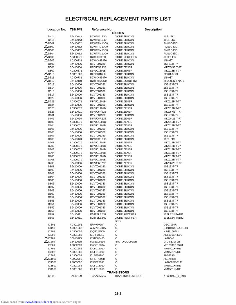
ELECTRICAL REPLACEMENT PARTS LIST
Location No. TSB P/N Reference No. DescriptionDIODES
D414 BZ410043 D2WT011E10 DIODE,SILICON 11E1-EICD415 BZ410043 D2WT011E10 DIODE,SILICON 11E1-EIC
! D501 BZ410062 D2WTRM11C0 DIODE,SILICON RM11C-EIC ! D502 BZ410062 D2WTRM11C0 DIODE,SILICON RM11C-EIC ! D503 BZ410062 D2WTRM11C0 DIODE,SILICON RM11C-EIC ! D504 BZ410062 D2WTRM11C0 DIODE,SILICON RM11C-EIC ! D505 AD300076 D28F30DF60 DIODE,RECTIFIER 30DF6-FC ! D506 AD300731 D2WXN49370 DIODE,SILICON 1N4937
D507 BZ410006 D1VT001330 DIODE,SILICON 1SS133T-77D508 BZ410064 D97U03R91B DIODE,ZENER MTZJ3.9B T-77D509 AD300671 D97U01801B DIODE,ZENER MTZJ18B T-77
! D510 AD301980 D2CF2016L0 DIODE,SILICON FE201-6L49 ! D511 AD300731 D2WXN49370 DIODE,SILICON 1N4937 ! D512 BZ410010 D28T21DQN9 DIODE,SCHOTTKY 21DQ09N-TA2B1
D513 BZ410006 D1VT001330 DIODE,SILICON 1SS133T-77D514 BZ410006 D1VT001330 DIODE,SILICON 1SS133T-77D516 BZ410006 D1VT001330 DIODE,SILICON 1SS133T-77D517 BZ410006 D1VT001330 DIODE,SILICON 1SS133T-77D520 BZ410006 D1VT001330 DIODE,SILICON 1SS133T-77
! D523 AD300671 D97U01801B DIODE,ZENER MTZJ18B T-77D524 BZ410006 D1VT001330 DIODE,SILICON 1SS133T-77D525 AD300070 D97U01201B DIODE,ZENER MTZJ12B T-77D528 BZ410021 D97U05R61B DIODE,ZENER MTZJ5.6B T-77D601 BZ410006 D1VT001330 DIODE,SILICON 1SS133T-77D602 BZ410058 D97U08R21B DIODE,ZENER MTZJ8.2B T-77D603 AD300670 D97U01501B DIODE,ZENER MTZJ15B T-77D604 AD300070 D97U01201B DIODE,ZENER MTZJ12B T-77D605 BZ410006 D1VT001330 DIODE,SILICON 1SS133T-77D606 BZ410006 D1VT001330 DIODE,SILICON 1SS133T-77D607 BZ410006 D1VT001330 DIODE,SILICON 1SS133T-77D608 BZ410043 D2WT011E10 DIODE,SILICON 11E1-EICD701 AD300070 D97U01201B DIODE,ZENER MTZJ12B T-77D702 AD300070 D97U01201B DIODE,ZENER MTZJ12B T-77D703 AD300070 D97U01201B DIODE,ZENER MTZJ12B T-77D704 AD300070 D97U01201B DIODE,ZENER MTZJ12B T-77D705 AD300070 D97U01201B DIODE,ZENER MTZJ12B T-77D706 AD300070 D97U01201B DIODE,ZENER MTZJ12B T-77D709 BZ410066 D97U06R21B DIODE,ZENER MTZJ6.2B T-77D801 BZ410006 D1VT001330 DIODE,SILICON 1SS133T-77D802 BZ410006 D1VT001330 DIODE,SILICON 1SS133T-77D803 BZ410006 D1VT001330 DIODE,SILICON 1SS133T-77D804 BZ410006 D1VT001330 DIODE,SILICON 1SS133T-77D805 BZ410006 D1VT001330 DIODE,SILICON 1SS133T-77D806 BZ410006 D1VT001330 DIODE,SILICON 1SS133T-77D807 BZ410006 D1VT001330 DIODE,SILICON 1SS133T-77D808 BZ410006 D1VT001330 DIODE,SILICON 1SS133T-77D809 BZ410006 D1VT001330 DIODE,SILICON 1SS133T-77D852 BZ410006 D1VT001330 DIODE,SILICON 1SS133T-77D853 BZ410006 D1VT001330 DIODE,SILICON 1SS133T-77D854 BZ410006 D1VT001330 DIODE,SILICON 1SS133T-77D855 BZ410006 D1VT001330 DIODE,SILICON 1SS133T-77D856 BZ410006 D1VT001330 DIODE,SILICON 1SS133T-77D857 BZ410011 D28TELS2N2 DIODE,RECTIFER 10ELS2N-TA1B2D858 BZ410011 D28TELS2N2 DIODE,RECTIFER 10ELS2N-TA1B2
ICSIC101 AD301981 I56F07090A IC OEC7090AIC199 AD301982 A3M701Z015 IC S-24C16AFJA-TB-01IC301 AD300055 I0QF021500 IC NJM2150AMIC302 AD301983 I01FF58910 IC AN5891SA-E1V
! IC401 BZ611025 I03TD80400 IC LA78040 ! IC504 BZ410088 0002E00610 PHOTO COUPLER LTV-817M-VB
IC601 AE002803 I06FC1283A IC M61283FP R70TIC701 AD301988 I0UF015010 IC MM1501XNREIC702 AD301988 I0UF015010 IC MM1501XNREIC902 AD300059 I01FF58290 IC AN5829S
! IC1001 AE003081 I0FSP7808B IC AN17808BIC1501 AE003002 I03FE76605 IC LA76605M-TLMIC1502 AD301988 I0UF015010 IC MM1501XNREIC1503 AD301988 I0UF015010 IC MM1501XNRE
TRANSISTORSQ101 BZ510109 TCAA3875SY TRANSISTOR,SILICON KTC3875S_Y_RTK
J2-2
Downloaded from www.Manualslib.com manuals search engine

ELECTRICAL REPLACEMENT PARTS LIST
Location No. TSB P/N Reference No. DescriptionTRANSISTORS
Q103 BZ510109 TCAA3875SY TRANSISTOR,SILICON KTC3875S_Y_RTK ! Q402 BZ510097 TCAT03227Y TRANSISTOR,SILICON KTC3227_Y-AT ! Q405 BZ510040 TDUU024990 TRANSISTOR,SILICON 2SD2499(LB0EC1) ! Q502 BZ510098 T220033260 FET 2SK3326(2) ! Q503 BZ510005 TA3T1371A0 TRANSISTOR,SILICON 2SA1371(D,E)-AE
Q504 BZ510069 TCATC31980 TRANSISTOR,SILICON KTC3198-AT(Y,GR) ! Q505 BZ510011 TC3T029090 TRANSISTOR,SILICON 2SC2909(S,T)-AA ! Q507 BZ510069 TCATC31980 TRANSISTOR,SILICON KTC3198-AT(Y,GR) ! Q508 BZ510077 TAAT012714 TRANSISTOR,SILICON KTA1271_Y-AT
Q509 BZ510069 TCATC31980 TRANSISTOR,SILICON KTC3198-AT(Y,GR) ! Q512 BZ510004 TA3T016240 TRANSISTOR,SILICON 2SA1624-AA ! Q514 BZ510070 TCAT032034 TRANSISTOR,SILICON KTC3203_Y-AT
Q601 BZ510105 TCAT03209Y TRANSISTOR,SILICON KTC3209_Y-ATQ602 BZ510105 TCAT03209Y TRANSISTOR,SILICON KTC3209_Y-ATQ603 BZ510109 TCAA3875SY TRANSISTOR,SILICON KTC3875S_Y_RTKQ604 BZ510105 TCAT03209Y TRANSISTOR,SILICON KTC3209_Y-ATQ605 BZ510109 TCAA3875SY TRANSISTOR,SILICON KTC3875S_Y_RTKQ606 BZ510105 TCAT03209Y TRANSISTOR,SILICON KTC3209_Y-ATQ607 BZ510070 TCAT032034 TRANSISTOR,SILICON KTC3203_Y-ATQ610 BZ510109 TCAA3875SY TRANSISTOR,SILICON KTC3875S_Y_RTKQ611 BZ510105 TCAT03209Y TRANSISTOR,SILICON KTC3209_Y-ATQ613 BZ510109 TCAA3875SY TRANSISTOR,SILICON KTC3875S_Y_RTKQ614 BZ510108 TAAA1504SY TRANSISTOR,SILICON KTA1504S_Y_RTKQ709 BZ510108 TAAA1504SY TRANSISTOR,SILICON KTA1504S_Y_RTKQ711 BZ510109 TCAA3875SY TRANSISTOR,SILICON KTC3875S_Y_RTKQ712 BZ510109 TCAA3875SY TRANSISTOR,SILICON KTC3875S_Y_RTK
! Q801 BZ510091 TCA0042170 TRANSISTOR,SILICON KTC4217(O,Y) ! Q802 BZ510091 TCA0042170 TRANSISTOR,SILICON KTC4217(O,Y) ! Q803 BZ510091 TCA0042170 TRANSISTOR,SILICON KTC4217(O,Y) ! Q810 AD301032 TCATC3199Y TRANSISTOR,SILICON KTC3199_Y-AT ! Q811 AD301032 TCATC3199Y TRANSISTOR,SILICON KTC3199_Y-AT ! Q812 AD301032 TCATC3199Y TRANSISTOR,SILICON KTC3199_Y-AT
Q852 BZ510069 TCATC31980 TRANSISTOR,SILICON KTC3198-AT(Y,GR)Q853 AD300024 TCUT00752Y TRANSISTOR,SILICON 2SC752(G)(TM)_YQ854 BZ510069 TCATC31980 TRANSISTOR,SILICON KTC3198-AT(Y,GR)Q855 BZ510069 TCATC31980 TRANSISTOR,SILICON KTC3198-AT(Y,GR)Q856 BZ510069 TCATC31980 TRANSISTOR,SILICON KTC3198-AT(Y,GR)Q857 BZ510073 TAATA12660 TRANSISTOR,SILICON KTA1266-AT(Y,GR)Q858 AD300029 TAU0018370 TRANSISTOR,SILICON 2SA1837Q859 AD300025 TCU0047930 TRANSISTOR,SILICON 2SC4793Q901 BZ510108 TAAA1504SY TRANSISTOR,SILICON KTA1504S_Y_RTKQ902 BZ510108 TAAA1504SY TRANSISTOR,SILICON KTA1504S_Y_RTKQ1001 BZ510068 TNAAJ05003 COMPOUND TRANSISTOR KRC111SRTKQ1503 BZ510109 TCAA3875SY TRANSISTOR,SILICON KTC3875S_Y_RTKQ1504 BZ510109 TCAA3875SY TRANSISTOR,SILICON KTC3875S_Y_RTKQ1507 BZ510109 TCAA3875SY TRANSISTOR,SILICON KTC3875S_Y_RTKQ1508 BZ510109 TCAA3875SY TRANSISTOR,SILICON KTC3875S_Y_RTK
COILS &TRANSFORMERSL301 BZ310041 02167F101J COIL 100 UHL401 BZ310004 021679472K COIL 4.7 MHL402 BZ310063 022100027A COIL,LINEARITY ELH5L4113
! L501 AD300119 029T000097 COIL,LINE FILTER 1R5A123F28Y ! L503 BZ310066 028R200024 COIL,DEGAUSS 8R200024
L601 AD301989 0216A6330J COIL 33 UHL802 AD300123 021673151K COIL 150 UHL803 AD300123 021673151K COIL 150 UHL804 AD300123 021673151K COIL 150 UHL901 BZ310041 02167F101J COIL 100 UHL1501 BZ310041 02167F101J COIL 100 UHL1502 AD301417 02167F221J COIL 220 UHL1503 AD301417 02167F221J COIL 220 UHL1505 AD300613 02167F150J COIL 15 UHL1508 BZ310041 02167F101J COIL 100 UHL1510 AD300613 02167F150J COIL 15 UHL1511 AD300613 02167F150J COIL 15 UHL1512 AD301608 0216A6220J COIL 22 UHT401 BZ310172 045013003J TRANS,HORIZONTAL DRIVE ETH14Y47AY
! T501 AD301034 048140066S TRANSFORMER,SWITCHING 8140066SJACKS
J701 AD301038 060J431019 RCA JACK MSP-213V2-432 PBSNJ702 AD300108 063Q700002 JACK YKF51-5503
J2-3
Downloaded from www.Manualslib.com manuals search engine

ELECTRICAL REPLACEMENT PARTS LIST
Location No. TSB P/N Reference No. DescriptionJACKS
J703 AD301038 060J431019 RCA JACK MSP-213V2-432 PBSNJ704 AD301037 060J411024 RCA JACK MSP-213V1-652 PBSNJ705 AD300110 060G401047 RCA JACK HTJ-032-03AYJ706 AD300111 060G401046 RCA JACK HTJ-032-03AWJ707 AD300112 060G401039 RCA JACK HTJ-032-03ARJ708 AD301038 060J431019 RCA JACK MSP-213V2-432 PBSN
! J801 BZ614115 066C130017 SOCKET,CATHODE RAY TUBE CVT3275-5101 ! J1001 BZ614361 060J131015 HEADPHONE JACK MSJ-2000
SWITCHESSW101 BZ612010 0504101T34 SWITCH,TACT EVQ21505RSW102 BZ612010 0504101T34 SWITCH,TACT EVQ21505RSW103 BZ612010 0504101T34 SWITCH,TACT EVQ21505RSW104 BZ612010 0504101T34 SWITCH,TACT EVQ21505RSW105 BZ612010 0504101T34 SWITCH,TACT EVQ21505R
VARIABLE RESISTORSVR401 BZ210108 V116313BTC VOLUME,SEMI FIXED EVNCYAA03B13VR502 BZ210101 V1163H4BTC VOLUME,SEMI FIXED EVNCYAA03BE4
P.C.BOARD ASSEMBLIESPCB010 AE003171 A3M7110010 PCB ASS'Y TMC559DPCB060 AE003172 A3M7110060 PCB ASS'Y TEAA93BPCB110 AE003173 A3M7110110 PCB ASS'Y TCA391B
MISCELLANEOUSB401 BZ310129 024HT03564 CORE,BEADS W4BRH3.5X6X1.0B402 BZ310129 024HT03564 CORE,BEADS W4BRH3.5X6X1.0B403 BZ310122 024HT03563 CORE,BEADS W4BRH3.5X6X1.0X2B405 BZ310129 024HT03564 CORE,BEADS W4BRH3.5X6X1.0B501 BZ310045 024AT03481 CORE,BEADS BL02RN1-R62T2B504 BZ310121 024HT03553 CORE,BEADS W5RH3.5X5X1.0B851 BZ310121 024HT03553 CORE,BEADS W5RH3.5X5X1.0B852 BZ310121 024HT03553 CORE,BEADS W5RH3.5X5X1.0B853 BZ310121 024HT03553 CORE,BEADS W5RH3.5X5X1.0BT001 AE000012 1412004008 BATTERY,MANGAN R03(AB)E_2P_GBT002 AE000012 1412004008 BATTERY,MANGAN R03(AB)E_2P_G
! CD501 AD300746 120R615901 CORD,AC BUSH 0R615901CD801 AD301042 06CU253401 CORD,CONNECTOR CU253401CD802 AD301994 06CU274201 CORD,CONNECTOR CU274201CD803 AD300094 06CP83035A CORD,CONNECTOR CP83035ACD851 AD301995 06CU244201 CORD,CONNECTOR CU244201CD852 AD301043 06CU232001 CORD,CONNECTOR CU232001CP101 BZ614102 0694270139 CONNECTOR PCB SIDE 173979-7
! CP401 AD300095 069X460029 CONNECTOR PCB SIDE B06B-DVS ! CP501 BZ614176 069S320419 CONNECTOR PCB SIDE A3963WV2-3PD ! CP502 AD300687 069S420110 CONNECTOR PCB SIDE A1561WV2-2P
CP507 BZ614444 069D01001A CONNECTOR PCB SIDE 003P-2100CP508 BZ614444 069D01001A CONNECTOR PCB SIDE 003P-2100CP803 AD301996 069S330010 CONNECTOR PCB SIDE A2361WV2-3PCP804 BZ614058 069W010010 CONNECTOR PCB SIDE 005P-2100CP852 BZ614350 069S230629 CONNECTOR PCB SIDE A2001WV2-3PCD1001 AD300093 06CU14411A CORD,CONNECTOR CU14411ACP1001 AD301045 069S140419 CONNECTOR PCB SIDE A2502WV2-4PCP801A BZ614276 067U005049 WIRE HOLDER B2013H02-5PCP801B AD300752 069S250629 CONNECTOR PCB SIDE A2001WV2-5PCP802A AD301997 067U007029 WIRE HOLDER B2013H02-7PCP802B BZ614485 069S270629 CONNECTOR PCB SIDE A2001WV2-7PCP851A BZ614334 067U004029 WIRE HOLDER B2013H02-4PCP851B AD301998 069S240629 CONNECTOR PCB SIDE A2001WV2-4PCP852B BZ614349 067U003029 WIRE HOLDER B2013H02-3PEL001 BZ614044 124120301A EYE LET XRY20X30BDEL002 BZ614043 124116281A EYE LET XRY16X28BD
! F501 AD301046 081PC6R305 FUSE 51MS063L ! FB401 AE003174 043220060F TRANSFORMER,FLYBACK FJN20A002_M
FH501 AE002634 06710T0009 HOLDER,FUSE EYF-52BCYFH502 AE002634 06710T0009 HOLDER,FUSE EYF-52BCYOS101 AD301048 0773071001 REMOTE RECEIVER RPM7138-WH5
! RY501 AD300114 0560V20115 RELAY ALKS321 ! SP1001 AD301050 070C457003 SPEAKER SG05K07BRA ! SP1002 AD301050 070C457003 SPEAKER SG05K07BRA ! TH501 AD302000 D8EE0B1400 DEGAUSS ELEMENT B59203-S1060-B14
TM101 AE003009 076R0GW020 TRANSMITTER R25-1943 ! TU001 AE000273 0163300005 RF UNIT 115-V-K015AR_B
J2-4
Downloaded from www.Manualslib.com manuals search engine

ELECTRICAL REPLACEMENT PARTS LIST
Location No. TSB P/N Reference No. DescriptionJACKS
! V801 AD301053 098W210437 CRT W/DY A51LVV896X07(O)X101 AD302002 100CT8R005 CRYSTAL HC-49/U-SX602 AD302003 100CT3R505 CRYSTAL HC-49/C
RESISTORRC................... CARBON RESISTOR
CAPACITORSCC................... CERAMIC CAPACITORCE................... ALUMI ELECTROLYTIC CAPACITORCP................... POLYESTER CAPACITORCPP.................. POLYPROPYLENE CAPACITORCPL.................. PLASTIC CAPACITORCMP................... METAL POLYESTER CAPACITORCMPL................ METAL PLASTIC CAPACITORCMPP................ METAL POLYPROPYLENE CAPACITOR
J2-5
Downloaded from www.Manualslib.com manuals search engine

TOSHIBA CORPORATION1-1, SHIBAURA 1-CHOME, MINATO-KU, TOKYO 105-8001, JAPAN
Downloaded from www.Manualslib.com manuals search engine


