73
Combinational Logic and Verilog

Combinational Logic and
Verilog

Programmable Array Logic
PAL

Example of PAL. GAL16V8C

Figure 6-26. PAL16L8
PALs 1. SOP
2. Multi-level
3. Flip-flops
4. 10 Inputs
5. 8 Inputs/output

Figure 6-28. General CPLD architecture
Complex PLD

4*3 PLA in CMOS logic

AND plane of EEPLD using floating-gate MOS transistors
EEPLDs•Floating gate
•Non-floating gate

Decoders

General Structure of a Decoder circuit

Example 1: Truth table for a 2-to-4 binary decoder.
Example of a decoder circuit
enable

2-to-4 decoder inside
enable

Verilog for 2-to-4 decoder
Structural type of description in Verilog

Example 2:Position encoding for a 3-bit mechanical encoding disk

Example 2 continued: Using a 3-to-8 decoder to decode a Gray code.

Example 3:74x138 3-to-8
decoder

Example 3: 74x138 3-to-8 decoder
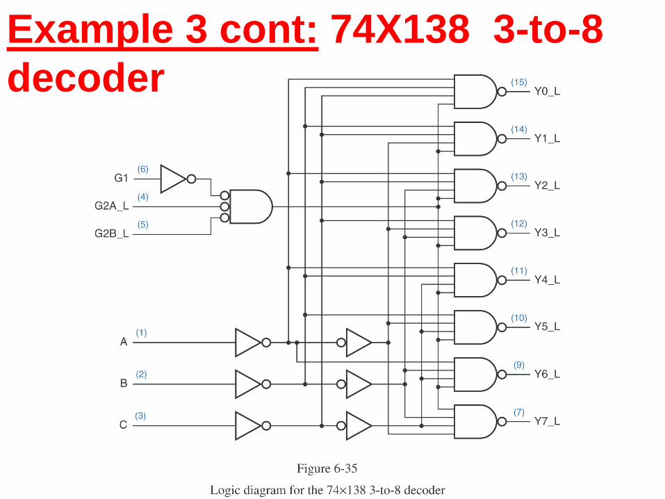
Example 3 cont: 74X138 3-to-8 decoder

Verilog code for 3-to-8 decoder
15..7

Verilog for 3-to-8 decoder
A[2]
A[1]
A[0]
Y_L[0]
Y_L[1]
Y_L[2]
Y_L[3]
Y_L[4]
Y_L[5]
Y_L[7]

74X138 Decoder:
Active level handling

74x138 like decoder with Active level handling
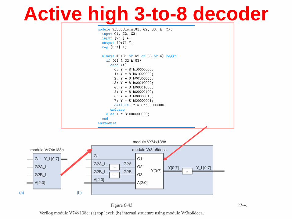
Active high 3-to-8 decoder

Behavioral Verilog for 3-to-8 decoder

Example 3 cont: 74x138 3-to-8 decoder
Default signal names

Example 3 cont: Symbols for 74x138
Incorrect because of double negations

Example 3 cont: 5-to-32 decoder from 74X138 chips
Global enable goes to inputs G1 and G2A
Chip select goes to input G2B

Example 3 cont: 4-to-16 decoder using 74X138
N3

Example 3 cont: 74x138 decoder using GAL
74x138 decoder can be built in single GAL 16V8 chip

Figure 6-41. 74x138-like decoder

Example: Customized decoder function

Customized decoder circuit Using 74X138

Seven Segment Display and
Decoder

Seven Segment Display
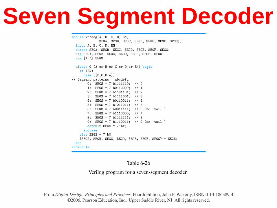
Seven Segment Decoder

EncodersWe already used encoders to design control logic for data path blocks

Encoders2n requests

Priority Encoders

Encoders
Any subset if 2n
requests
Number n of prioritized request

Encoders

8-input Priority Encoder
enable

15-input Priority Encoder in PLD
outputsinputs

Priority Encoder – handle 32 requests

8-input Priority Encoder

Three stateBuffers

Various three-state buffers

Eight sources sharing a three-state party line
Use of three-state buffers

Timing diagram for the three-state party line

74x541 Octal three-state buffer

Three-State buffers in
microprocessors

74x541 as a microprocessor input port.

Verilog module for a 74x540-like 8-bit three-state driver

74x245 octal three-state transceiver

Verilog module for a 74x245-like 8-bit transceiver

Bidirectional buses and transceiver operation

Bus selection codes for a four-way bus transceiver

PLD inputs and outputs for a four-way, 2-bit bus transceiver

Verilog module for a four-way, 2-bit bus transceiver

Multiplexers
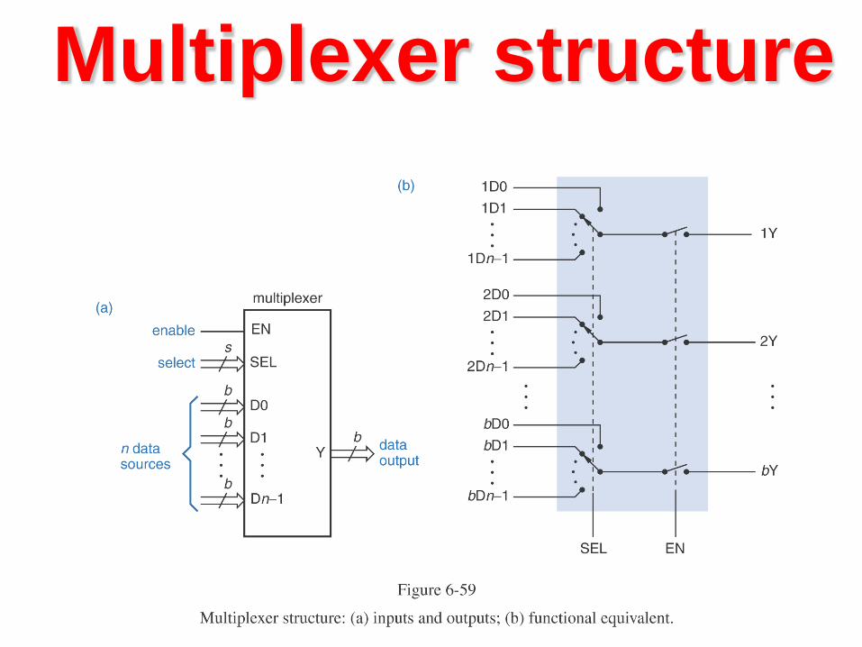
Multiplexer structure

74x151 8-input, 1-bit mux

74x151 8-input, 1-bit mux

Combining 74x151s to make a 32-to-1 multiplexer
Decoding and enabling

74x157 2-input 4-bit mux

GAL16V8 used as a 74x157 multiplexer
2 inputs, each 4 bits

Buffers to handle large fanout

A mux driving a bus and a demux receiving the bus

Decoders as demultiplexers

3-to-8 binary decoder as a demultiplexer

GALs as multiplexers

Function table for a SPECIALIZED 4-input, 18-bit
mux.

Behavioral Verilog for a specialized 4-input 18-bit mux

Dataflow Verilog for a 4-input, 8-bit mux

Behavioral Verilog for a 4-input, 8-bit mux.


