Comparative Performance Analysis of Lead-Free Perovskites Solar Cells by Numerical Simulation Shristy Srivastava Central University of Jharkhand Anand Kumar Singh Central University of Jharkhand Prashant Kumar Central University of Jharkhand Basudev Pradhan ( [email protected]) Central University of Jharkhand Research Article Keywords: Lead free perovskites, SCAPS-1D, Simulation, CsSnI3, eィciency Posted Date: June 4th, 2021 DOI: https://doi.org/10.21203/rs.3.rs-583148/v1 License: This work is licensed under a Creative Commons Attribution 4.0 International License. Read Full License
Transcript
Comparative Performance Analysis of Lead-FreePerovskites Solar Cells by Numerical SimulationShristy Srivastava
Central University of JharkhandAnand Kumar Singh
Central University of JharkhandPrashant Kumar
Central University of JharkhandBasudev Pradhan ( [email protected] )
Central University of Jharkhand
Research Article
Keywords: Lead free perovskites, SCAPS-1D, Simulation, CsSnI3, e�ciency
Posted Date: June 4th, 2021
DOI: https://doi.org/10.21203/rs.3.rs-583148/v1
License: This work is licensed under a Creative Commons Attribution 4.0 International License. Read Full License
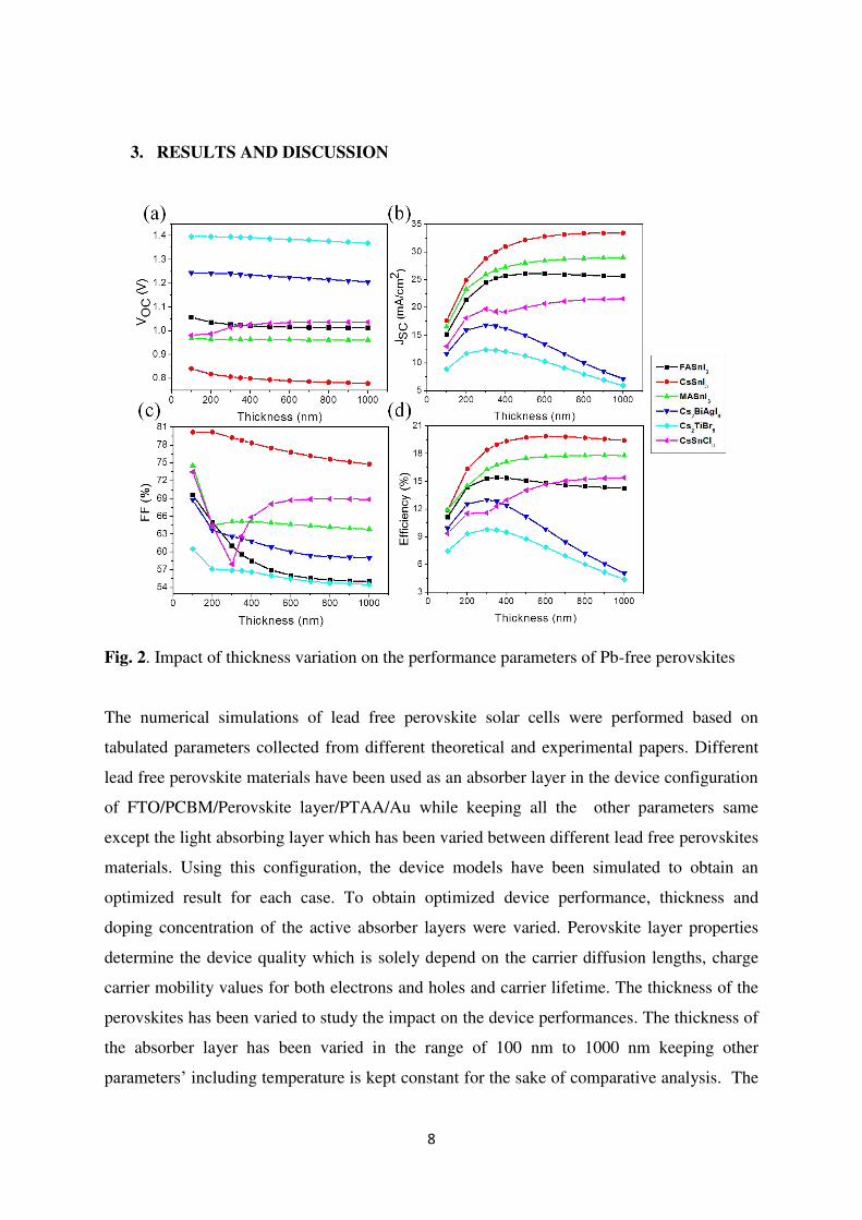
Fig. 2. Impact of thickness variation on the performance parameters of Pb-free perovskites
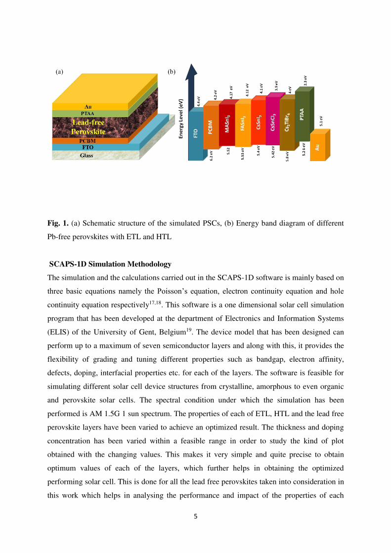
The numerical simulations of lead free perovskite solar cells were performed based on
tabulated parameters collected from different theoretical and experimental papers. Different
lead free perovskite materials have been used as an absorber layer in the device configuration
of FTO/PCBM/Perovskite layer/PTAA/Au while keeping all the other parameters same
except the light absorbing layer which has been varied between different lead free perovskites
materials. Using this configuration, the device models have been simulated to obtain an
optimized result for each case. To obtain optimized device performance, thickness and
doping concentration of the active absorber layers were varied. Perovskite layer properties
determine the device quality which is solely depend on the carrier diffusion lengths, charge
carrier mobility values for both electrons and holes and carrier lifetime. The thickness of the
perovskites has been varied to study the impact on the device performances. The thickness of
the absorber layer has been varied in the range of 100 nm to 1000 nm keeping other
parameters’ including temperature is kept constant for the sake of comparative analysis. The
9
impact of thickness variation on the performance parameters of different Pb-free perovskites
is shown in the Fig. 2. As the thickness increases, the open circuit voltage (VOC) decreases or
nearly remains the same for most of the perovskites shown in Fig. 2a. An uncommon
behaviour is observed for CsSnCl3 where the VOC increases with thickness and then remains
constant. The reason for this could be attributed to interfacial kinetics due to band energy
mismatch. The nature of curves obtained for short circuit current density (JSC) and efficiency
(η) versus thickness is nearly same as depicted in Fig. 2b and 2d. As the thickness of absorber
increases, the JSC and η value increases, and reaches to the optimum value and decrease
slowly with the increase of layer thickness for all perovskite materials, but the optimum
thickness in which PCE reaches to highest value is different for different perovskite materials
with which varies between 300 nm to 500 nm under this configuration. This trend could be
explained by the fact that with the increase in active layer thickness more light absorption
occurs in the device, that implies more charge carrier generation, and higher light generated
current which ultimately leads to higher JSC and efficiency28. Further increase in thickness
may exceed the diffusion length of these materials, causing an increase in the recombination
rate of charge carriers leading to increased saturation current, hence decreased VOC, and also
JSC which ultimately reduces efficiency. But, in some specific materials, such as FASnI3,
Cs2BiAgI6, and Cs2TiBr6 the values increase to a certain point and then decreases very fast
with the increase of thickness. This may be because for these materials, after a certain point,
the increase in absorber thickness leads to increased series resistance and back contact
recombination hence leading to reduce JSC and ɳ. The fill factor plot (Fig. 2c) shows a
decrease in value as the perovskite thickness increases and this could be explained by
describing the FF dependency on perovskite layer thickness. Since, FF signifies how easily
electron- hole pairs move through the device without recombination. With increased
perovskite layer thickness, charge pathway resistance should increase leading to decrease in
FF. On the other hand, internal recombination inside the lead-free perovskite material,
occurred due to the short life time of electron (tn) and hole (tp) charge carriers, which do not
permit adequate period for charge carrier to develop conduction band at lead-free perovskite
material20. Certain abnormality of FF in case CsSnCl3 with the increase of active layer
thickness was also observed.
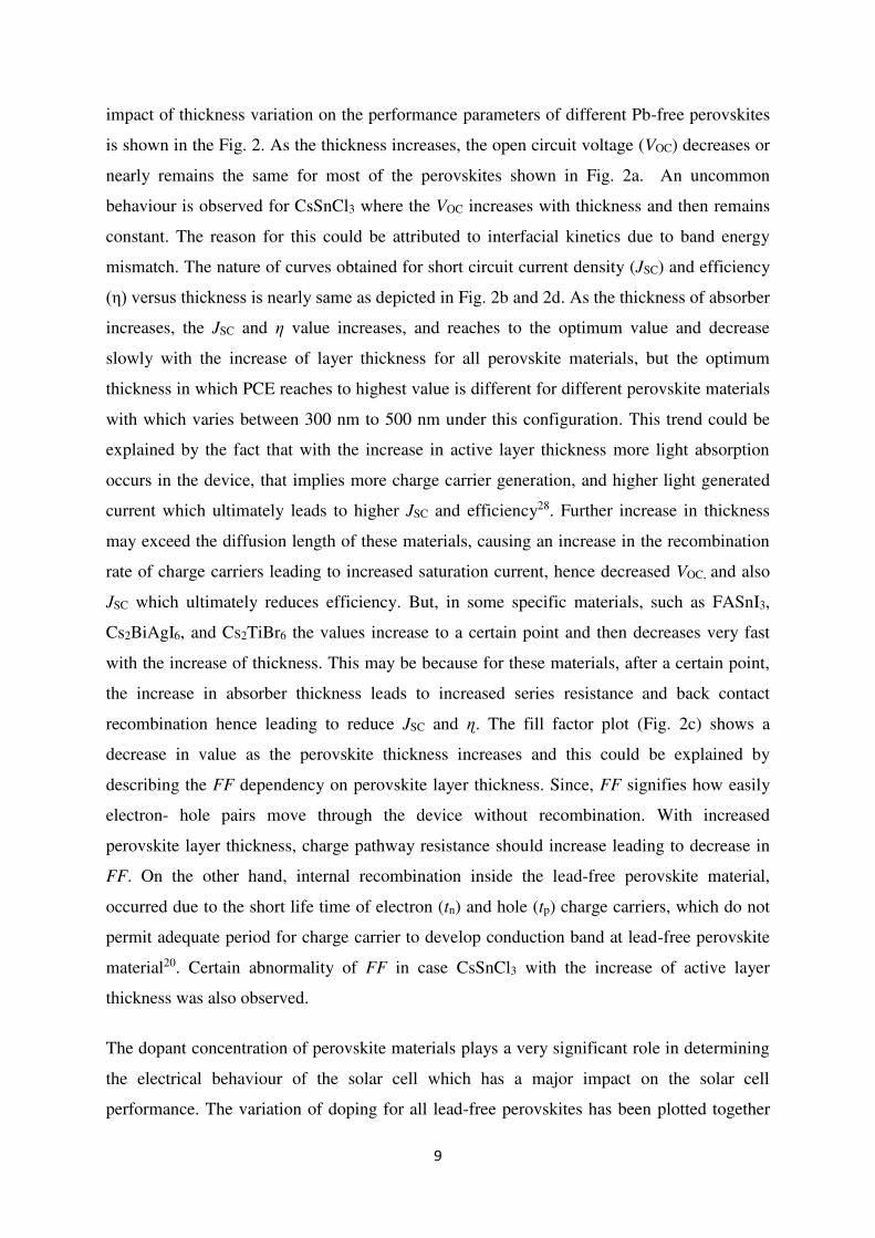
The dopant concentration of perovskite materials plays a very significant role in determining
the electrical behaviour of the solar cell which has a major impact on the solar cell
performance. The variation of doping for all lead-free perovskites has been plotted together
10
as a function of the solar cell performance parameters. The doping of the absorber layer has
been varied in the range of 1×10¹⁴ to 5×1020 cm-3. Rest all the properties are kept constant
and the impact has been studied by comparing the behaviour of various materials. The figure
3 shows impact on different solar cell parameters due to the variation of doping concentration
in different absorber materials. The open circuit voltage of all perovskite materials increase
steadily with the increase of doping concentration as shown in Fig. 3a, reverse saturation
current decrease with the increase of doping concentration, which leads to the increase in
open circuit voltage29,30. On that hand built in potential (Vbi) as shown in the equation 10 is
strongly dependent on the doping concentration. 𝑉𝑏𝑖 = 𝑘𝑇𝑞 ln 𝑁𝐴𝑁𝐷𝑛𝑖2 (10)
where k is Boltzmann constant, T is temperature, q is the electron charge, ni is intrinsic
concentration, ND is donor doping concentration and NA is acceptor doping concentration. As
the doping concentration increases the Vbi also increases which get reflected in VOC. The
maximum VOC is observed for Cs2TiBr6 (1.8eV) based device where as the lowest for CsSnI3
(1.3eV) based device, other perovskites following the trend which is adequate because open
circuit voltage is increasing with the increase in bandgap. The short circuit current densities
of all the Pb-free perovskites decrease with the increase in doping as shown in Fig. 3b. Lower
doping concentration serves for higher carrier collection due to a wider depletion region,
increased doping levels leads to narrow charge collection region, hence, reduced JSC at higher
doping. The materials with higher band gaps have lower JSC values and vice versa VOC curve
trend. The fill factor for most of the perovskites is seen to first decrease and then increases
with the increase in doping values after which it remains almost constant, while a continuous
increase in FF is observed for FASnI3 and CsSnI3 as shown in the Fig. 3c. The efficiency of
most materials are seen to increase with increase in doping values while a decrease in ɳ is
observed in MASnI3 and Cs2TiBr6 while for Cs2BiAgI6, initially it decreases and then
increases slowly as shown in Fig. 3d. The nature obtained in this case is highly dependent on
the behaviour each material reflects in the previous three performance parameters, hence,
decrease in ɳ of MASnI3 and Cs2TiBr6 due to decrease in FF and JSC. The explanation for
such nature of FF and ɳ could be due to decreased resistance with easy charge carrier
pathway because of increased doping concentration.
11
Fig. 3. Impact of doping variation on the performance parameters of Pb-free perovskites
12
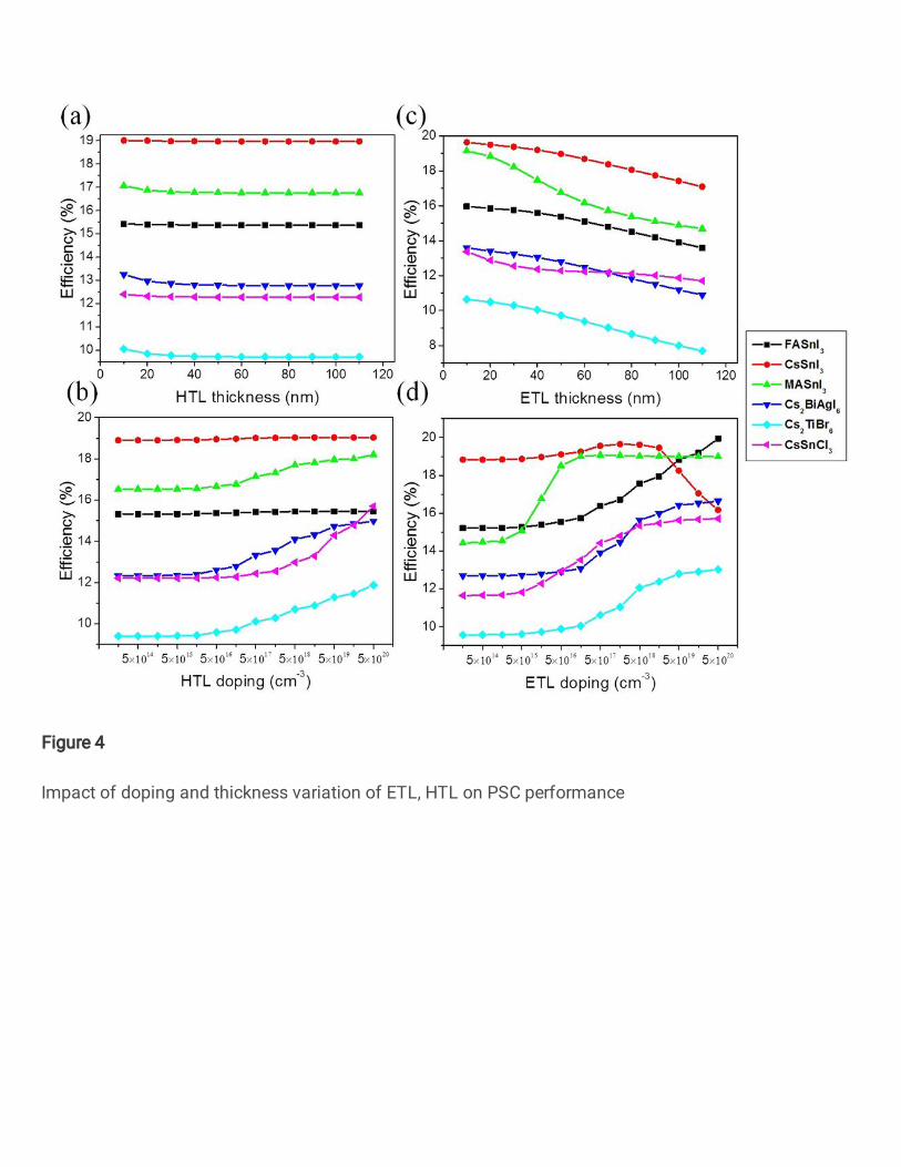
Fig. 4. Impact of doping and thickness variation of ETL, HTL on PSC performance
The variation in doping and thickness of the HTL layer i.e. PTAA has very negligible impact
on the performance parameters of all the perovskites. As the figure 4a suggests, initially ɳ
decreases negligibly with the increase in HTL thickness and later it becomes constant for all
perovskite based devices suggesting no major impact of HTL thickness on device PCE.
Contrary to it a slight increase in the efficiency is observed as the HTL doping increases
whereas, the value remain nearly constant in case of FASnI3 and CsSnI3 based devices as
shown in Fig.4b. Electron transport layer aids in modifying the interface, controlling the
charge recombination rates and also aligning the interfacial energy levels. The efficiency of
all perovskite based devices decreases with the increase of ETL layer thickness which is
shown in the Fig. 4c. On the other hand, Fig. 4d shows efficiency slowly increases with
increase of the ETL doping. A continuous increase in the efficiency values are observed with
the increase in doping of ETL, except for CsSnI3 which after 1019 cm-3 doping value
experiences a decrease in efficiency whereas in case of MaSnI3 efficiency remain constant
13
after 1017 cm-3 doping concentration. Over all the efficiency increases slowly with the
increase of HTL and ETL doping for most of the perovskites and become constant. As the
donor concentration increases the conductivity also increases which reduces device JSC and it
maintains a constant value. After the certain limit of donor concentration the solar cell
performance parameters remains unchanged due to Moss-Burstein effect31. Increase in
doping of HTM and ETM layers also enhances the interface electric field between the HTL
and ETL, this increased electric potential used to separate the excitons with less
recombination rate and the performance of the device is increased. Alternatively, moderate
doping is also needed whereas heavy doping leads to increased recombination and the
perovskite semi-conductive nature changes to metallic which obstructs the carrier transport
mechanism32.
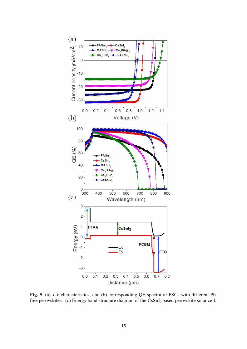
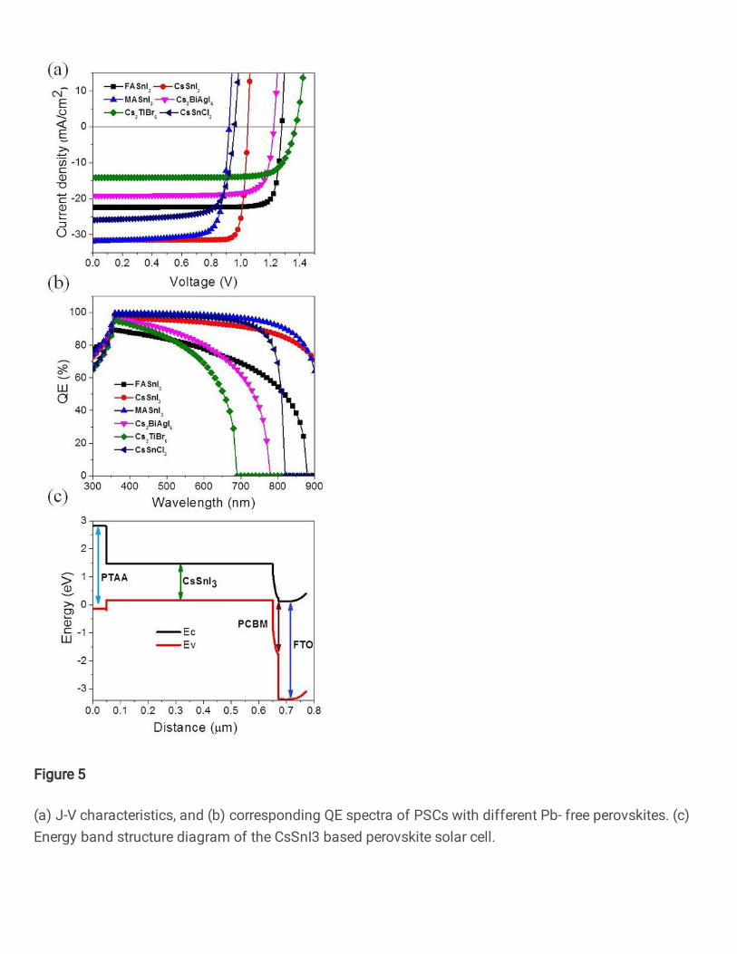
The J-V characteristics and quantum efficiency curve in light conditions for various lead-free
perovskite materials have been plotted under optimized conditions as shown in the figure 5a
and 5b respectively. All the devices show very good J-V characteristics. CsSnI3 having the
lowest band gap has the broadest absorption spectrum and Cs2TiBr6 having the narrowest of
all, rest materials falling in order. However, as per the QE curves obtained, the working
devices with best QE is CsSnCl3, MASnI3 and CsSnI3 respectively as their active layers, with
minimum energy losses with maximum QE values obtained at 98.4%, 99.7% and 96.67%
respectively. The QE values at the low wavelength region for these materials suggest that the
electrons due to the high energy photons are efficiently generated and collected. On the other
hand it also reflected that the front surface is well passivated. In the high wavelength region,
a high QE is observed in MASnI3 and CsSnI3 based device, which ultimately leads to higher
short circuit current. The table 2 represents the performance parameters obtained for six
different Pb-free perovskites based solar cells, when simulated under AM 1.5G 1sun spec,
300K temperature and all other working conditions same. Among all the devices, FASnI3
shows highest VOC of 1.277 V, whereas MASnI3 shows lowest VOC of 0.921 V. The device
with MASnI3 shows highest short circuit current density of 31.85mA/cm2. CsSnI3 and
FASnI3 based device shows higher FF as compare other devices. Figure 5c shows the energy
band diagram of CsSnI3 based perovskite with PTAA as hole transport layer and PCBM as
electron transport layer from the SCAPS-1D software. Overall CsSnI3 based device shows
highest power conversion efficiency of 28.97 % with VOC of 1.048 V, JSC of 31.85mA/cm2
and FF of 87.66% among the other perovskite based solar cells, which is so far the highest
reported value in this configuration by any simulation method. The high performance of
CsSnI3 based solar cell would be due to small optical bandgap of perovskite material
14
combined with high optical absorption coefficient and low exciton binding energy. At the
same time it also shows high electron dimensionality33, relatively high intrinsic or
thermodynamic stability34. It was also observed from the generation and recombination depth
profile of the charge carrier that the charge carrier generation is high at PCBM and perovskite
interface and carrier recombination is less whereas in the PTAA and perovskite interface,
generation is less and carrier recombination is high. Therefore, from this simulation work, it
is clear that CsSnI3 based lead free perovskite solar cell definite be best alternate to the lead
based perovskite solar cells.
Table 2: Performance parameters for optimized devices with various Pb-free perovskites
Pb- free
Perovskite
VOC
(V)
JSC
(mA/cm2)
FF
(%)
Efficiency
(%)
FASnI3 1.277 22.40 86.36 24.70
CsSnCl3 0.959 25.92 74.31 18.47
MASnI3 0.921 31.85 77.81 22.82
Cs2BiAgI6 1.087 19.94 74.87 16.23
Cs2TiBr6 1.313 11.81 79.40 12.31
CsSnI3 1.048 31.53 87.66 28.97
15
Fig. 5. (a) J-V characteristics, and (b) corresponding QE spectra of PSCs with different Pb-
free perovskites. (c) Energy band structure diagram of the CsSnI3 based perovskite solar cell.
16
4. CONCLUSION
In summary, comprehensive performance analysis of different lead-free perovskite based
solar cells has been investigated by numerical simulation on SCAPS-1D. Detail comparative
study has been performed to study the impact of different perovskite material properties,
doping, thickness, and their impact on the PCE on the same device configuration having HTL
as PTAA and ETL as PCBM. We have optimized different properties like doping density, the
thickness of active materials as well as hole and electron transport layers for the further
improvement of the device performance. Among all the lead-free perovskite based devices,
CsSnI3 based device shows the highest power conversion efficiency of 28.97 % with VOC of
1.048 V, JSC of 31.85mA/cm2, and FF of 87.66%. So based on our simulation study, it is
clear that lead-free perovskite based solar cells definitely guide the scientific community for
further exploration towards experimental realization in lead-free perovskite based solar cells
in the future.
Acknowledgement
BP would like to thank to Department of Science and Technology (Project No. -SB/FTP/PS-
148/2013, SR/S2/RJN-55/2012, and DST/TM/CERI/C199) for financial support. The authors
are also grateful to Ministry of Human Resources and Development (MHRD) for their
financial support (project No. F.No. 5-5/2014-TS.Vll).
References
1 Correa-Baena, J.-P. et al. The rapid evolution of highly efficient perovskite solar cells. Energy Environ. Sci. 10, 710-727 (2017).
2 Correa-Baena, J.-P. et al. Promises and challenges of perovskite solar cells. Science 358, 739-744 (2017).
3 Kojima, A., Teshima, K., Shirai, Y. & Miyasaka, T. Organometal halide perovskites as visible-light sensitizers for photovoltaic cells. J. Am. Chem. Soc. 131, 6050-6051 (2009).
4 https://www.nrel.gov/pv/cell-efficiency.html,” can be found under https://www.nrel.gov/pv/cell-efficiency.html.
5 Jena, A. K., Kulkarni, A. & Miyasaka, T. Halide perovskite photovoltaics: background, status, and future prospects. Chem. Rev. 119, 3036-3103 (2019).
6 Nishimura, K. et al. Lead-free tin-halide perovskite solar cells with 13% efficiency. Nano Energy 74, 104858 (2020).
7 Shi, T. et al. Effects of organic cations on the defect physics of tin halide perovskites. Journal of Materials Chemistry A 5, 15124-15129 (2017).
8 Gupta, S., Cahen, D. & Hodes, G. How SnF2 impacts the material properties of lead-free tin perovskites. J. Phys. Chem. C 122, 13926-13936 (2018).
9 Milot, R. L. et al. Radiative monomolecular recombination boosts amplified spontaneous emission in HC (NH2) 2SnI3 perovskite films. The journal of physical chemistry letters 7, 4178-4184 (2016).
10 Hao, F., Stoumpos, C. C., Cao, D. H., Chang, R. P. & Kanatzidis, M. G. Lead-free solid-state organic–inorganic halide perovskite solar cells. Nature photonics 8, 489-494 (2014).
11 Lee, S. J. et al. Fabrication of efficient formamidinium tin iodide perovskite solar cells through SnF2–pyrazine complex. J. Am. Chem. Soc. 138, 3974-3977 (2016).
12 Kumar, M. H. et al. Lead‐free halide perovskite solar cells with high photocurrents realized through vacancy modulation. Adv. Mater. 26, 7122-7127 (2014).
13 Zhao, Z. et al. Mixed‐organic‐cation tin iodide for lead‐free perovskite solar cells with an efficiency of 8.12%. Adv. Sci. 4, 1700204 (2017).
14 Abdelaziz, S., Zekry, A., Shaker, A. & Abouelatta, M. Investigating the performance of formamidinium tin-based perovskite solar cell by SCAPS device simulation. Opt. Mater. 101, 109738 (2020).
15 Noel, N. K. et al. Lead-free organic–inorganic tin halide perovskites for photovoltaic applications. Energy Environ. Sci. 7, 3061-3068 (2014).
16 Ke, W. & Kanatzidis, M. G. Prospects for low-toxicity lead-free perovskite solar cells. Nat. Commun. 10, 1-4 (2019).
17 Raoui, Y. et al. Performance analysis of MAPbI3 based perovskite solar cells employing diverse charge selective contacts: Simulation study. Solar Energy 193, 948-955 (2019).
18 Duan, Q. et al. Design of hole-transport-material free CH3NH3PbI3/CsSnI3 all-perovskite heterojunction efficient solar cells by device simulation. Solar Energy 201, 555-560 (2020).
19 Burgelman, M., Nollet, P. & Degrave, S. Modelling polycrystalline semiconductor solar cells. Thin Solid Films 361, 527-532 (2000).
20 Kumar, M., Raj, A., Kumar, A. & Anshul, A. An optimized lead-free formamidinium Sn-based perovskite solar cell design for high power conversion efficiency by SCAPS simulation. Opt. Mater. 108, 110213 (2020).
21 Smith, B. Efficient Lead-Free Perovskite Solar Cell. (2018). 22 Owolabi, J. A., Onimisi, M. Y., Ukwenya, J. A., Bature, A. B. & Ushiekpan, U.
R. Investigating the Effect of ZnSe (ETM) and Cu2O (HTM) on Absorber Layer on the Performance of Pervoskite Solar Cell Using SCAPS-1D. Am J Phys Appl 8, 1 (2020).
23 Coulibaly, A. B., Oyedele, S. O. & Aka, B. Comparative study of lead-free perovskite solar cells using different hole transporter materials. Modeling and Numerical Simulation of Material Science 9, 97-107 (2019).
24 Madan, J., Pandey, R. & Sharma, R. Device simulation of 17.3% efficient lead-free all-perovskite tandem solar cell. Solar Energy 197, 212-221 (2020).
25 Li, S. et al. The investigation of inverted pin planar perovskite solar cells based on FASnI3 films. Sol. Energy Mater. Sol. Cells 199, 75-82 (2019).
18
26 Khattak, Y. H., Baig, F., Shuja, A., Beg, S. & Soucase, B. M. Numerical analysis guidelines for the design of efficient novel nip structures for perovskite solar cell. Solar Energy 207, 579-591 (2020).
27 Singh, A. K., Srivastava, S., Mahapatra, A., Baral, J. K. & Pradhan, B. Performance optimization of lead free-MASnI3 based solar cell with 27% efficiency by numerical simulation. Opt. Mater. 117, 111193 (2021).
28 Koh, T. M. et al. Formamidinium tin-based perovskite with low E g for photovoltaic applications. Journal of Materials Chemistry A 3, 14996-15000 (2015).
29 Lin, L. et al. Boosting efficiency up to 25% for HTL-free carbon-based perovskite solar cells by gradient doping using SCAPS simulation. Solar Energy 215, 328-334 (2021).
30 Maram, D. K., Haghighi, M., Shekoofa, O., Habibiyan, H. & Ghafoorifard, H. A modeling study on utilizing ultra-thin inorganic HTLs in inverted p–n homojunction perovskite solar cells. Solar Energy 213, 1-12 (2021).
31 Trukhanov, V., Bruevich, V. & Paraschuk, D. Y. Effect of doping on performance of organic solar cells. Physical Review B 84, 205318 (2011).
32 Stoumpos, C. C., Malliakas, C. D. & Kanatzidis, M. G. Semiconducting tin and lead iodide perovskites with organic cations: phase transitions, high mobilities, and near-infrared photoluminescent properties. Inorganic chemistry 52, 9019-9038 (2013).
33 Xiao, Z., Song, Z. & Yan, Y. From Lead halide Perovskites to Lead‐free metal halide Perovskites and Perovskite derivatives. Adv. Mater. 31, 1803792 (2019).
34 Zhou, Y. & Zhao, Y. Chemical stability and instability of inorganic halide perovskites. Energy Environ. Sci. 12, 1495-1511 (2019).
Figures
Figure 1
(a) Schematic structure of the simulated PSCs, (b) Energy band diagram of different Pb-free perovskiteswith ETL and HTL
Figure 2
Impact of thickness variation on the performance parameters of Pb-free perovskites
Figure 3
Impact of doping variation on the performance parameters of Pb-free perovskites
Figure 4
Impact of doping and thickness variation of ETL, HTL on PSC performance
Figure 5
(a) J-V characteristics, and (b) corresponding QE spectra of PSCs with different Pb- free perovskites. (c)Energy band structure diagram of the CsSnI3 based perovskite solar cell.