Page 1
254 | P a g e
COMPARATIVE STUDY OF DIODE CLAMPED,
FLYING CAPACITOR AND H-BRIDGE MULTILEVEL
INVERTER HARMONICS REDUCTION
Md Ajmal Nayab1, Mr. Zafar Khan
2
1Student, M.Tech, Department of Electrical & Electronics Engineering, Al-falah University, (India)
2Associate Prof., Department of Electrical & Electronics Engineering, Al-falah University, (India)
ABSTRACT
The power electronics device which converts DC power to AC power at required output voltage and frequency level
is known as inverter. The voltage source inverters produce an output voltage or a current with levels either 0 or +ve
or-ve V dc. They are known as two-level inverters. Multilevel inverter is to synthesize a near sinusoidal voltage from
several levels of dc voltages. Multilevel inverter has advantage like minimum harmonic distortion. Multi-level
inverters are emerging as the new breed of power converter options for high power applications. They typically
synthesize the stair-case voltage waveform (from several dc sources) which has reduced harmonic content. This
thesis compares three different topologies of inverters (5- level inverter, Diode clamped inverter, 5-level Flying
capacitor clamped inverter and 5-level Cascaded H-bridge inverter). In this model of five-level Three Phase Diode
clamped inverter, Flying capacitor clamped inverter and Cascaded H-Bridge inverter has been developed using
MOSFETS IGBT. Gating signals for these MOSFETS have been generated by designing comparators. In order to
maintain the different voltage levels at appropriate intervals, the conduction time intervals of MOSFETS have been
maintained by controlling the pulse width of gating pulses (by varying the reference signals magnitude of the
comparator). The result is compared with simulation results. Simulation models (designed in SIMULINK) have been
developed up to five levels and THD in all the cases have been identified.
Keywords: Multilevel, Diode Clamped, Flying Capacitor, H-Bridge, Cascade, Harmonics, Modulation,
MATLAB/SIMULINK, %THD.
I. INTRODUCTION
The need for high power apparatus in industry has increased in recent years. Multilevel converters have developed
as easy alternatives for such power requirements. Mostly used in medium voltage applications, multilevel converters
have gained prominence since it is not feasible to connect a single power semiconductor switch directly to the grid.
There are other advantages of multilevel converters such as their capability to be easily interfaced with the
Page 2
255 | P a g e
renewable energy sources such as solar power, wind power, and fuel cells.Multilevel converters consist of a group
of semiconductor switches, like IGBTs, and a set of voltage source components like capacitors or independent
sources. The basic concept of these converters depends on using this series of switches and sources to synthesize a
stepped or staircase output voltage waveform. Therefore, they reduce the voltage stress on each device or
component used . Multilevel converters play a significant role in enhancing the quality of high power distribution
networks, power conditioning systems, variable speed drive systems etc because of the availability of higher number
of voltage levels at the output. This helps in reducing the size of switching components which can be operated at
lower switching frequencies. However, multilevel converters have their own disadvantages. Voltage sharing may
not be as desired under all conditions because of the series connection of the switching devices.
II. MULTILEVEL INVERTER
1. 5-level diode clamped multilevel inverter
Diode-clamped inverters are one of the earliest designed topologies of multilevel inverters. Figure 2.1 shows a
single phase five-level diode-clamped inverter. The two capacitors connected in the circuit split input voltage Vdc to
obtain the midpoint voltage of the input. In a three level topology, the common point of capacitors is connected to
the ground. Therefore, this circuit can also be called the neutral point clamped inverter. Diodes D1 and D2 present in
the circuit help with clamping dc voltage Vdc to obtain different output voltage levels. There are nine allowable
switching states for the given circuit to obtain five different output voltage levels +Vdc, +Vdc /2, 0, -Vdc/2, and –
Vdc. It has to be noted that switch pairs Sa1 and Sa1׳, and Sa2 and Sa2 ׳ are complementary to each other. Similarly,
switch pairs Sb1 and Sb1׳, and Sb2 and Sb2 ׳ are complementary to each other.
Fig. 1 Three phase diode clamped inverter.
The number of switches, capacitors, and diodes required in the circuit increases with the number of output voltage
levels desired. For every additional level of voltage, it requires an extra pair of complementary switches is required
Page 3
256 | P a g e
in each limb of the circuit and also additional capacitors and clamping diodes. However, in such cases, voltage
balancing of the capacitors and the cost of diodes become a practical problem. Another disadvantage of diode-
clamped multilevel inverters is that they need high voltage rating diodes to block the reverse voltages.
2. 5-level flying capacitor multilevel inverters
The diodes in the diode-clamped topology can be replaced by clamping capacitors or floating capacitors to clamp
the voltages. Such a topology is called flying capacitor multilevel inverter (FCMLI). FCMLI topologies are
relatively new compared to the diode-clamped the cascaded H-bridge cell inverter topologies. Redundancy in the
switching states is available by using flying capacitors instead of clamping diodes. This redundancy can be used to
regulate the capacitor voltages and obtain the same desired level of voltage at the output. Figure2 shows a single-
phase five-level FCMLI topology. The voltage across the capacitors is considered to be half of Dc source voltage
Vdc. The output voltage consists of five different voltage levels + Vdc, Vdc/2, 0, -Vdc/2, and - Vdc. Similar to the
other multilevel converter topologies, FCMLI also has complementary switch pairs. In the present considered
circuit, switches Sa1 &Sa1 ׳, and Sa2 &Sa2 ׳ are complementary to each other.Similarly on the other limb, switches
Sb1 &Sb1 ׳, and Sb2 &Sb2׳ are complementary to each other. The switching states available for such a topology are
higher than that of the diode clamped. The number of voltage levels at the output can be increased by adding a pair
of complementary switches and a capacitor. However, all the capacitors used in such topologies must be rated
identically which can prove to be expensive and bulky in size. Single-phase five-level FCMLI topology VdcCa
CbSa1Sa2
Fig.2.Three phase 5-level Flying capacitor multilevel inverter
3. Cascaded H-bridge multilevel inverter.
Cascaded H-bridge multilevel inverter topology is a series connection of two or more individual full bridge
inverters. Figure 3 shows a single-phase, five-level cascaded H-bridge cell inverter realized by connecting two three
Page 4
257 | P a g e
level conventional full bridge inverters in series. Switch pairs Sa1 and Sa1׳, and Sa2 and Sa2 ׳ are complementary to
each other. Similarly, switch pairs of the other full bridge inverter Sb1 and Sb1׳, and Sb2 and Sb2 ׳ are
complementary to each other. The different voltage levels that can be obtained at the output terminals are +2Vdc,
+Vdc, 0, Vdc, -2Vdc. If the dc voltage sources in both the inverter circuits connected in series are not equal to each
other, then nine levels can be obtained at the output terminals. Thenumber of levels in the output voltage can be
increased by two by adding an identical inverter in series. Cascaded H-bridge cell inverters use the least number of
power electronic devices when compared to any other topology. However, they require isolated power sources in
each cell which in turn requires a large isolating transformer.
Fig.3 Three phase cascaded H-bridge multilevel inverter
The major challenge in the flying capacitor multilevel inverter topologies is the voltage regulation across the
capacitors. Therefore, the appropriate selection of switching states becomes a priority in FCMLI topologies.
III. CONTROL TECHNIQUES FOR MULTILEVEL INVERTER
1. Modulation
When it comes to multilevel inverter modulation there are basically two groups of methods: modulation with
fundamental switching frequency or high switching frequency PWM. For both cases a stepped output waveform is
achieved, but with the high switching frequency methods the steppes are modulated with some sort of PWM.
Independent of switching frequency choice there are, however, also space vector methods to choose from.
2. PWM for multilevel inverters
Multilevel PWM methods uses high switching frequency carrier waves in comparison to the reference waves to
generate a sinusoidal output wave, much like in the two-level PWM case. To reduce harmonic distortions in the
output signal phase-shifting techniques are used . There are several methods that change disposition of or shift
multiple triangularcarrier waves. The number of carrier waves used is dependent to the number of switches to be
controlled in the inverter. In addition to the two sinusoidal carrier wave modulation methods presented further down
there are also two more well known alternative methods that will not be discussed in this report: Alternative Position
Opposition Disposition (APOD) and Phase Opposition Disposition (POD).
Page 5
258 | P a g e
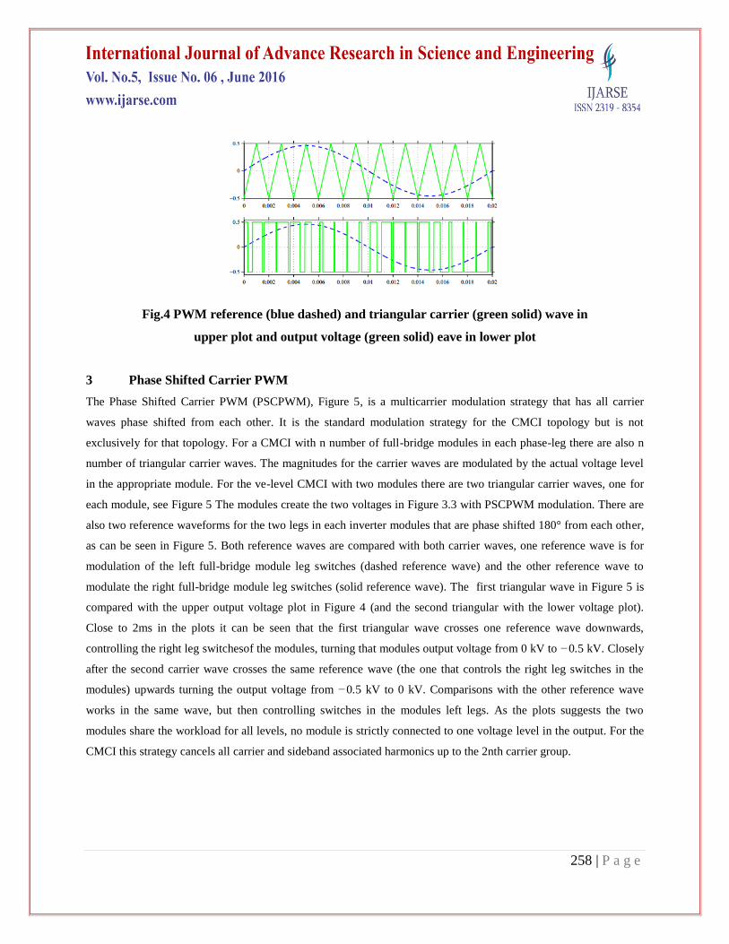
Fig.4 PWM reference (blue dashed) and triangular carrier (green solid) wave in
upper plot and output voltage (green solid) eave in lower plot
3 Phase Shifted Carrier PWM
The Phase Shifted Carrier PWM (PSCPWM), Figure 5, is a multicarrier modulation strategy that has all carrier
waves phase shifted from each other. It is the standard modulation strategy for the CMCI topology but is not
exclusively for that topology. For a CMCI with n number of full-bridge modules in each phase-leg there are also n
number of triangular carrier waves. The magnitudes for the carrier waves are modulated by the actual voltage level
in the appropriate module. For the ve-level CMCI with two modules there are two triangular carrier waves, one for
each module, see Figure 5 The modules create the two voltages in Figure 3.3 with PSCPWM modulation. There are
also two reference waveforms for the two legs in each inverter modules that are phase shifted 180° from each other,
as can be seen in Figure 5. Both reference waves are compared with both carrier waves, one reference wave is for
modulation of the left full-bridge module leg switches (dashed reference wave) and the other reference wave to
modulate the right full-bridge module leg switches (solid reference wave). The first triangular wave in Figure 5 is
compared with the upper output voltage plot in Figure 4 (and the second triangular with the lower voltage plot).
Close to 2ms in the plots it can be seen that the first triangular wave crosses one reference wave downwards,
controlling the right leg switchesof the modules, turning that modules output voltage from 0 kV to −0.5 kV. Closely
after the second carrier wave crosses the same reference wave (the one that controls the right leg switches in the
modules) upwards turning the output voltage from −0.5 kV to 0 kV. Comparisons with the other reference wave
works in the same wave, but then controlling switches in the modules left legs. As the plots suggests the two
modules share the workload for all levels, no module is strictly connected to one voltage level in the output. For the
CMCI this strategy cancels all carrier and sideband associated harmonics up to the 2nth carrier group.
Page 6
259 | P a g e
Fig.5 The carrier and reference waves for a wve-level CMCI with PSCPWM, two
reference waves and two triangular waves (one for each module).
4 Phase Distortion PWM
In Phase Distortion PWM (PDPWM), Figure 6 all carrier waves are in phase. A great acknowledgment for this
technique is that it is generally accepted as the method that creates the lowest harmonic distortion in line-to-line
voltage. When used for an NPCMLI with m number of voltage levels, m−1 number of triangular carrier waves is
used. These carrier waves have the same frequency and are arranged on top of each other, with no phase shift, so
that they together span from maximum output voltage to minimum output voltage. The carrier waves amplitudes
should be modulated with aspect of the current voltage magnitude for each respective voltage level, each carrier
wave is connected to a specific output voltage level. If the carrier waves are not modulated in this way the correct
output voltage will not be achieved if the sources voltage levels change from their supposed value (get unbalanced).
If the sources voltage amplitudes change without that the carrier waves are modulated with that change the correct
output voltage will not be generated during the during the correct time spans.
Fig.6The two module voltages, one in each plot, together with the achieved totaloutput voltage (blue
dashed line in both plots)
Page 7
260 | P a g e
When one carrier wave is crossed by the reference the output wave steps one level up or down with a switch
transaction. One carrier wave hence modulates the use of one voltage state. Only one level is modulated at any time,
as can be seen in the in Figure 6, sincethe reference only crosses one carrier at any level. The output voltage from
the PDPWM modulation with a-ve-level NPCMLI is shown in Figure 6
IV PROJECT DESIGN AND IMPLEMENTATION
1. Modelling of Five level diode clamped inverter
Fig. 7 Simulink model three phase 5 level diode clamped inverter & Switching block of three phase
5 level inverter.
2. Modeling Of Single Phase Flying Capacitor Multilevel Inverters
Fig.9 Simulink model of Three phase 5 level flying capacitor clamped inverter &Switching block of
three phase 5 level Flying capacitor clamped inverter.
Page 8
261 | P a g e
3. Modelling of single phase cascaded H-bridge multilevel inverter.
Fig.11 Three phase of a 5 level cascaded H-bridge inverter&Switching block of Three phase 5 level
cascaded H-bridge inverter
V SIMULATONS & RESULT
The multi-level inverter system is a very promising device in AC power drives when both reduced content and high
power are required. Up to now several multilevel topologies have been introduced. The main topologies are diode
clamped inverter, flying capacitor inverter, H-bridge inverter in order to generate a high voltage waveform using
low voltage devices. In this chapter, we are considering the simulation of three main topologies in multi level
inverter. Here we are going to have 5 level diode clamped inverter, flying capacitor inverter, H-bridge inverter.
1. Simulation of 5 level diode clamped inverter.
Fig.13 Output voltage without & with filtered voltage waveform of 5 level diode clamped inverter.
Page 9
262 | P a g e
Fig.15 FFT analysis output without & with filtered voltage waveform of 5 level diode clamped
inverter
2. Simulation of 5 Level Flying Capacitor Clamped Inverter
Figure 6.6 Output without & with filtered voltage of 5 level flying capacitor clamped inverter
Figure 6.9 FFT analysis of output without & with filtered voltage waveform of 5 level flying capacitor
clamped inverter
Page 10
263 | P a g e
3. Simulation of 5 level cascaded h-bridge inverter.
Figure 6.11 Output without & with filtered voltage waveform of 5 cascaded H- Bridge inverter.
Figure 6.14 FFT analysis of Output without & with filteredvoltage waveform of 5 cascaded H- Bridge
inverter.
5.1 RESULTS
From FFT analsysis of the three topologies we get the total harmonic distortion (THD) as follows:
VI CONCLUSION &FUTURE SCOPE
This work has presented several topologies for multilevel inverters (MLI), some of them
well known with applications on the market. Every topology have been described in
Controllers
THD of inverter output Line
Voltage (%)
THD of filtered Line
Voltage (%) Diode Clamped Multilevel
inverter
16.82% 0.28%
Flying Capacitor Multilevel
inverter
27.21% 0.36%
H bridge Multilevel inverter 27.21% 0.36%
Page 11
264 | P a g e
detail. Several modulation techniques have also been presented which are to be used
with the presented topologies. We hereby conclude that Multi-level inverters is a very promising technology in the
power industry. In this project, the advantages and applications of Multi-Level Inverters are mentioned and a
detailed description of different multi-level inverter topologies is presented. Single Phase H-Bridge Inverter, Diode
led and Flying capacitor multi level inverter functioning is realized virtually using MATLAB SIMULINK.
A detailed Multi-Level Inverter is presented from which we concluded that the harmonic content is greatly reduced
in Multi-Level Inverter and the Cascaded H-Bridge Inverter topology has advantage over the other two as it requires
less number of components as compared to the other two types of inverters and so its overall weight and price is also
less.This project can be extended further by increasing the number of levels in multilevel inverter. IC’s can be used
to generate gating pulses directly rather than designing them by using comparators and NOT gates. By using IC’s,
complexity in designing gate pulses can be reduced.
REFERENCES
[1] “Power Electronics Circuits, Devices & Applications” , Muhammad H. Rashid, Third Edition, Prentice Hall
India.
[2] Zhong Du, Leon M. Tolber, BurakOzpineci, John N. Chiasso, DC-AC Cascaded HBridge Multilevel Boost
Inverter With No Inductors for Electric/Hybrid Electric Vehicle Applications. 2009, Boise state university
[3] Martin Veenstra, INVESTIGATION AND CONTROL OF A HYBRID ASYMMETRIC MULTI-LEVEL
INVERTER FOR MEDIUM-VOLTAGE APPLICATIONS, 2003, Lausanne, EPFL
[4] L.M. Tolbert, F.Z. Peng, D.J. Adams, J.W. Mckeever, Multilevel inverters for large automotive electric drives,
1997, Darborn, Michigan
[5] K.T. Chau, Y.S. Wong, Overview of power management in hybrid electric vehicles, 2002, Energy conversion
and management 43
[6] Chris Mi, Fang. Z. Peng, Kenneth J. Kelly, Michael O’Keefe, VahabHassani, Topology, design, analysis and
thermal management of power electronics for hybrid electric vehicle applications, International journal of
Electric and Hybrid vehicles, Vol.1, 2008
[7] Fang Z. Peng, A Generalized Multilevel Inverter Topology with Self Voltage Balancing, IEEE transaction on
Industry applications, Vol. 37, 2001
[8] Leon M. Tolbert, John Chiasson, Keith McKenzie, Zhong Du, Elimination of harmonics in a multilevel
converter with non equal DC sources, IEEE transaction on Industry applications, Vol.41, 2005 [9] José
Rodríguez, Jih-Sheng Lai, Fang ZhengPeng, Multilevel Inverters: A Survey of Topologies, Controls and
Applications, IEEE transaction on Industry Electronics, Vol.49, 2002
[10] Leon M. Tolbert, Fang Z. Peng, Multilevel Converters as a Utility Interface for Renewable Energy Systems,
Power engineering society summer meeting, 2000, IEEE


![Type-1 and Type-2 Fuzzy Logic Controller Based Multilevel ... · types of multilevel inverters: cascaded H-bridge, diode clamped, flying capacitors [6]. The advantages of multilevel](https://static.documents.pub/doc/80x56/5f0b60b77e708231d43038d2/type-1-and-type-2-fuzzy-logic-controller-based-multilevel-types-of-multilevel.jpg)


