52
ESA-ESTEC GSTP - Analog Silicon Compiler for Mixed Signal ASICs Irradiation of CSA-PSA & Design of a CMOS High-Speed 8-bit 100MS/S ADC core

ESA-ESTEC GSTP - Analog SiliconCompiler for Mixed Signal ASICs
Irradiation of CSA-PSA&
Design of a CMOS High-Speed 8-bit100MS/S ADC core

Final presentation – ESA-ESTEC 7/3/2001 Jan Vandenbussche 2
Outline! Irradiation of CSA-PSA chip [designed and fabricated in ASTP4
project]" Objectives" Measurement setup" Measurements" Conclusions
! Design High-Speed 100MS/s 8-bit ADC" Objectives" Design methodology" Architectural level design" Device level design" Layout" Measurements" Conclusions

Final presentation – ESA-ESTEC 7/3/2001 Jan Vandenbussche 3
Irradiation CSA-PSA: objectives! Perform an initial evaluation of the total dose hardness of
the commercial 0.7µm CMOS process from MIETEC" radiation tolerance evaluation of standard CMOS technology
! Total dose testing on CSA-PSA chip :" designed and fabricated in ASTP4 project “VLSI Design Tools-
Module generation for analog silicon compilation” with theESTEC division of the ESA (Contract 9890/92/NL/GS).
! Workpackage" WP1200
Final presentation – ESA-ESTEC 7/3/2001 Jan Vandenbussche 4
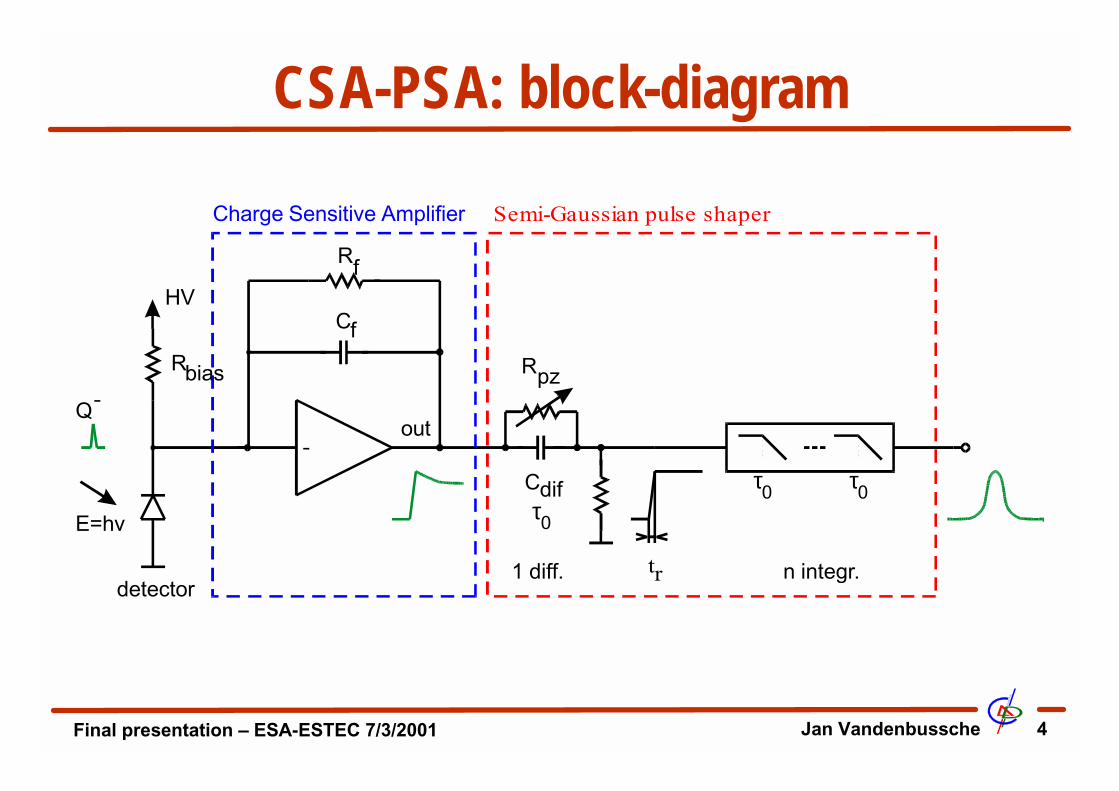
CSA-PSA: block-diagram
tr
C
fR
1 diff.
HV
Q
E=hv
-
Rbias
out-
n integr.
Rpz
ττCdif
0
0
Charge Sensitive Amplifier Semi-Gaussian pulse shaper
detector
τ0
f

Final presentation – ESA-ESTEC 7/3/2001 Jan Vandenbussche 5
CSA-PSA: micro photograph
CSA PSA
Integrator
Pole-zero
canceling
Differentiator
Rf

Final presentation – ESA-ESTEC 7/3/2001 Jan Vandenbussche 6
CSA-PSA: measurement setup! Compliant with AD3! Five samples were exposed to 50 krad! Two of them were afterwards exposed to 100 krad! Measurements:
" for good comparison additional noise and linearity measurementswere done before irradiating the samples
" for each sample 11 inputs were applied: varying from 5, 10, 20,30, 40, 50, 60, 70, 80, 90, 100fC
" for each input signal a histogram, comprising 30.000 samples,was measured
" linearity and noise were calculated from histograms

Final presentation – ESA-ESTEC 7/3/2001 Jan Vandenbussche 7
CSA-PSA: measurement results
0.5output voltage [V]
1000
500
00 1 1.5 2 0.5
output voltage [V]
1000
500
00 1 1.5 2 0.5
output voltage [V]
1000
500
00 1 1.5 2
0.5output voltage [V]
1000
500
00 1 1.5 2 0.5
output voltage [V]
1000
500
00 1 1.5 2 0.5
output voltage [V]
1000
500
00 1 1.5 2

Final presentation – ESA-ESTEC 7/3/2001 Jan Vandenbussche 8
CSA-PSA: measurement results cont’d
! gain:18mV/fC! peaking time: 1.14
µs! noise: 899 e-RMS! linearity < 0.5 %97 98 99 100 101 102 103
time [ sec]
Ou
tpu
t vo
ltag
e C
SA
-PS
A [
V]
-0.5
0
0.5
1.0
1.5
2.0
2.5
τp

Final presentation – ESA-ESTEC 7/3/2001 Jan Vandenbussche 9
CSA-PSA: measurement results cont’d
Input Charge [fC]
00
10
1.0
20
0.2
30
1.2
40
0.4
50
1.4
60
0.6
70
1.6
80
0.8
90
1.8
100
2.0
Ou
tpu
t vo
ltag
e [V
] Before irradiation

Final presentation – ESA-ESTEC 7/3/2001 Jan Vandenbussche 10
CSA-PSA: measurement results cont’d
0 10
1.0
20
0.2
30
1.2
40
0.4
50
1.4
60
0.6
70
1.6
80
0.8
90
0
100
ou
tpu
t vo
ltag
e
[V]
Input Charge [fC]
-0.2
After 50 krad

Final presentation – ESA-ESTEC 7/3/2001 Jan Vandenbussche 11
CSA-PSA: measurement results cont’d! After exposure to 50 krad
" a slight decrease in conversion gain: from 18mV/fC to 16mV/fC" the peaking time decreases slightly from 1.14 to 1.17µs" the noise level shows little change
! Conclusion 50 krad irradiation" all chips survived the irradiation testing of 50 krad quite good" only a slight decrease in performance is noticed" good recovery after 24 hours" full recovery after 168 hours.
Final presentation – ESA-ESTEC 7/3/2001 Jan Vandenbussche 12
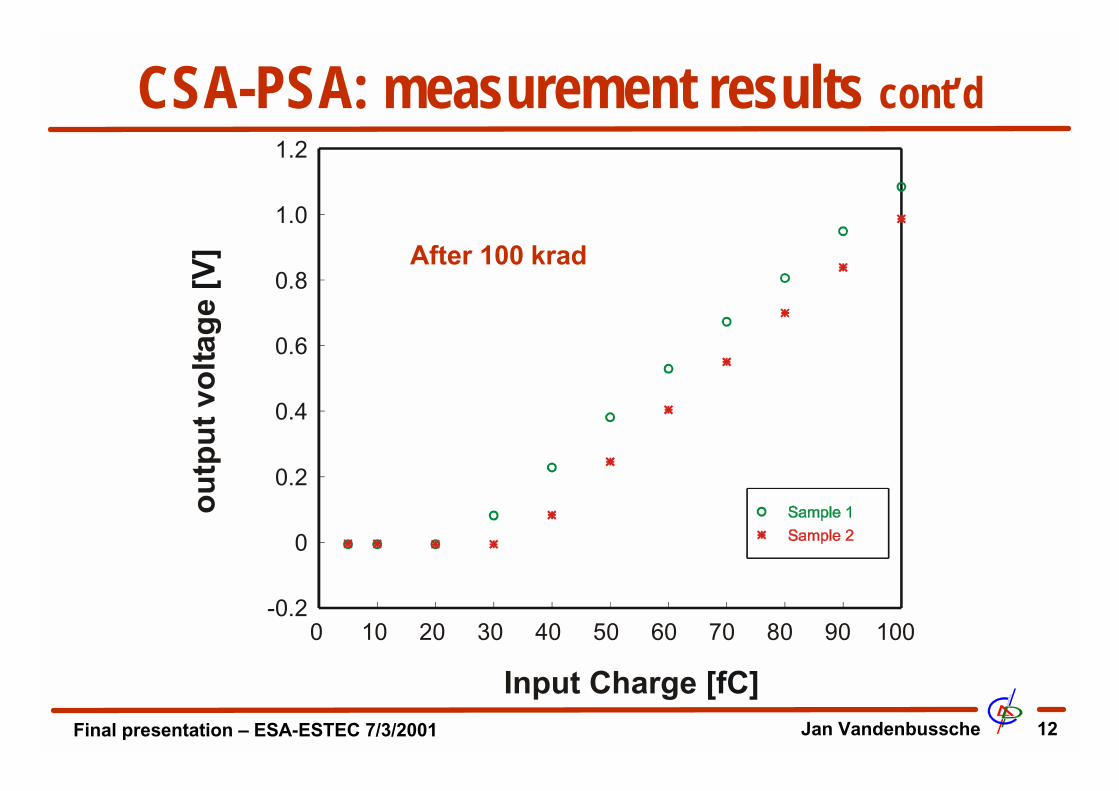
CSA-PSA: measurement results cont’d
0 10 20 30 40 50 60 70 80 90 100
Input Charge [fC]
1.0
0.2
1.2
0.4
0.6
0.8
0
-0.2
ou
tpu
t vo
ltag
e
[V] After 100 krad

Final presentation – ESA-ESTEC 7/3/2001 Jan Vandenbussche 13
CSA-PSA: measurement results cont’d! After exposure to 100 krad
" a further decrease in performance" the conversion gain dropped by a factor of two" the peaking time increased from 1.14µs to 1.20µs" the noise level increased slightly After 24 hours annealing little
recovery was seen, after 168 hours of annealing both sampleshad fully recovered from the irradiation
! Conclusion 100 krad irradiation" both samples survived irradiation" little recovery after 24 hours annealing" full recovery after 168 hours of annealing

Final presentation – ESA-ESTEC 7/3/2001 Jan Vandenbussche 14
CSA-PSA: conclusions! the Alcatel Microelectronics CMOS 0.7µm technology
shows good radiation tolerance! deep submicron CMOS technologies can be a viable
alternative to expensive radiation hard technology:" gate all around
! the sample set was too small to draw finalizingconclusions, but same message was heard on RadTolmeeting

Final presentation – ESA-ESTEC 7/3/2001 Jan Vandenbussche 15
CSA-PSA: conclusions cont’d! RadTol 49 meeting
" gate allround techniques for analog as well as digital libraries" promising results were presented at the RadTol meeting#plain CMOS is a true candidate for future space applications.
! Publications originating from this work" J. Vandenbussche, F. Leyn, G. Van der Plas, G. Gielen, "Total
Dose Testing of a Standad CMOS Particle Detector Front-End forSpace Applications", RadTol meeting R49, Geneve, October 281998.
" J. Vandenbussche, F. Leyn, G. Van der Plas, G. Gielen, and W.Sansen, "A Fully Integrated Low-Power CMOS Paritcle DetectorFront-End for Space Applications", IEEE Transactions onNuclear Science, Vol. 45, pp. 2262-2272, August 1998.

Final presentation – ESA-ESTEC 7/3/2001 Jan Vandenbussche 16
Outline! Irradiation of CSA-PSA chip
" Objectives" Measurement setup" Measurements" Conclusions
! Design High-Speed 100MS/s 8-bit ADC" Objectives" Design methodology" Architectural level design" Device level design" Layout" Measurements" Conclusions
Final presentation – ESA-ESTEC 7/3/2001 Jan Vandenbussche 17
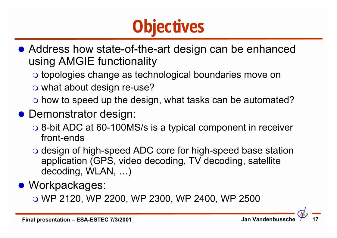
Objectives! Address how state-of-the-art design can be enhanced
using AMGIE functionality" topologies change as technological boundaries move on" what about design re-use?" how to speed up the design, what tasks can be automated?
! Demonstrator design:" 8-bit ADC at 60-100MS/s is a typical component in receiver
front-ends" design of high-speed ADC core for high-speed base station
application (GPS, video decoding, TV decoding, satellitedecoding, WLAN, …)
! Workpackages:" WP 2120, WP 2200, WP 2300, WP 2400, WP 2500
Final presentation – ESA-ESTEC 7/3/2001 Jan Vandenbussche 18
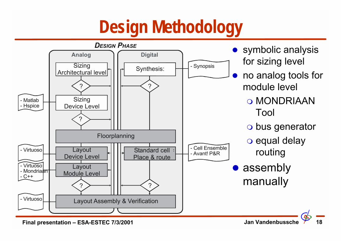
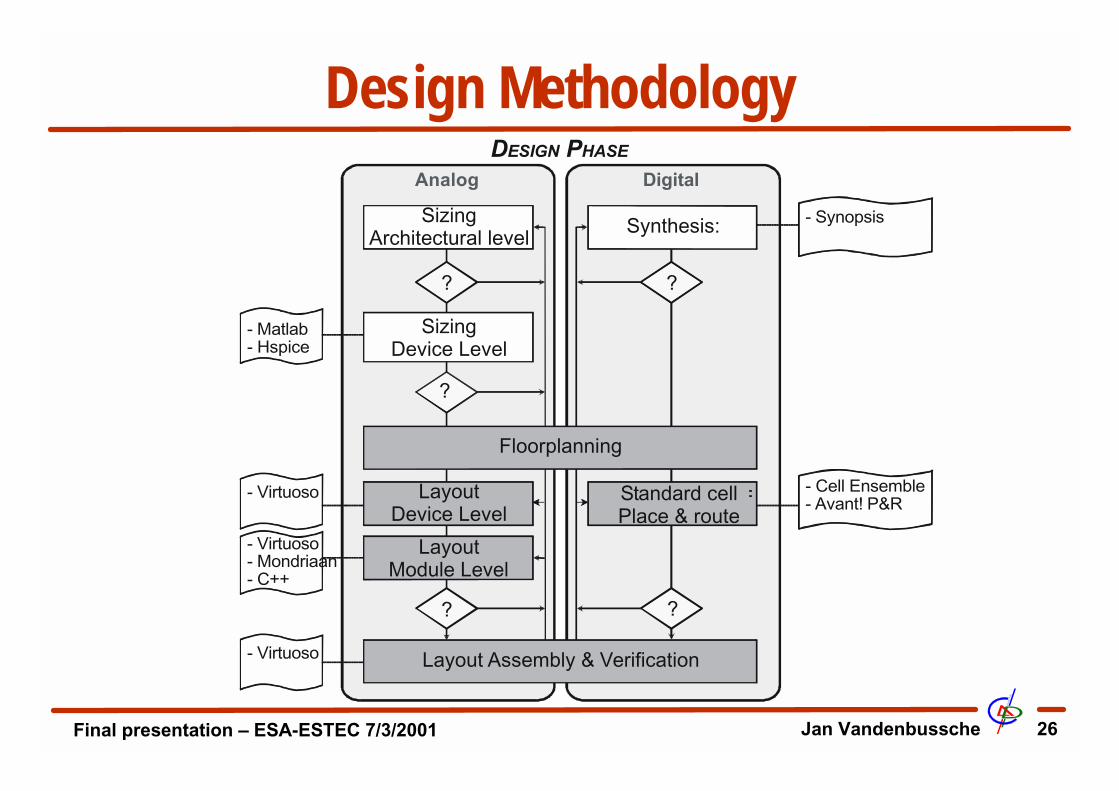
Design Methodology
Sizing Architectural level
? ?
?
?
?
Floorplanning
Layout Assembly & Verification
Synthesis:
Analog Digital
DESIGN PHASE
Sizing Device Level
Layout Device Level
Layout Module Level
Standard cell Place & route
- Matlab- Hspice
- Virtuoso
- Virtuoso- Mondriaan- C++
- Virtuoso
- Synopsis
- Cell Ensemble- Avant! P&R
! symbolic analysisfor sizing level
! no analog tools formodule level" MONDRIAAN
Tool" bus generator" equal delay
routing
! assemblymanually

Final presentation – ESA-ESTEC 7/3/2001 Jan Vandenbussche 19
Architectural Level: overview topologies
4
6
8
10
12
14
16
18
1K 10K 100K 1M 10M 100M 1G 10G
CMOSBipolar
GaAs
sigma-delta
multi-steppipelined
flash
fs [Hz]
bits
8-bit 100MS/s

Final presentation – ESA-ESTEC 7/3/2001 Jan Vandenbussche 20
Architectural Level: overview cont’d! Possible candidates for 8-bit 100MS/s ADC:
" pipelined architecture$ low power$ sampling speed shifts to higher frequencies as technology
scales down$no publications on such high-speed ‘working’ designs
" flash:$ consumes a lot of power$ intrinsically the fastest architecture with its full parallel
implementation$8-bit 80MS/s CMOS flash ADC has been published
#Only the flash architectures are capable of obtaining thetargeted specifications in the 0.35 µm CMOS technology

Final presentation – ESA-ESTEC 7/3/2001 Jan Vandenbussche 21
Architectural Level: Flash ADC! Problems classical flash ADC
" large power consumption (2N comparators)$ solution: folding
" large input capacitance, resulting in bandwidth limitations forinput signal frequencies$ solution: interpolation
" input feedthrough" kickback noise
! Additional improvements" averaging (Bult ISSCC ) by preamplifiers" new fully differential input stage" new enhanced comparator to avoid kickback noise
Final presentation – ESA-ESTEC 7/3/2001 Jan Vandenbussche 22
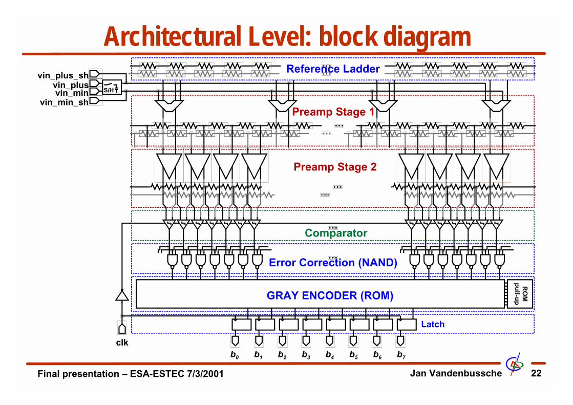
Architectural Level: block diagramReference Ladder
Preamp Stage 1
Comparator
Error Correction (NAND)
RO
Mp
ull-u
pGRAY ENCODER (ROM)
Latch
clk
vin_minvin_plus
vin_min_sh
vin_plus_sh
S/H
Preamp Stage 2
b0 b1 b2 b3 b4 b5 b6 b7

Final presentation – ESA-ESTEC 7/3/2001 Jan Vandenbussche 23
Architectural Level Design
How much equivalent inputreferred offset for INL/DNL < 0.5LSB with yield of 99.9%?
! Static performance:" INL/DNL < 0.5 LSB
with yield 99.9%" Monte-Carlo
simulations"
! Dynamic performance:...
LSBoffset 7.0<σ
Final presentation – ESA-ESTEC 7/3/2001 Jan Vandenbussche 24
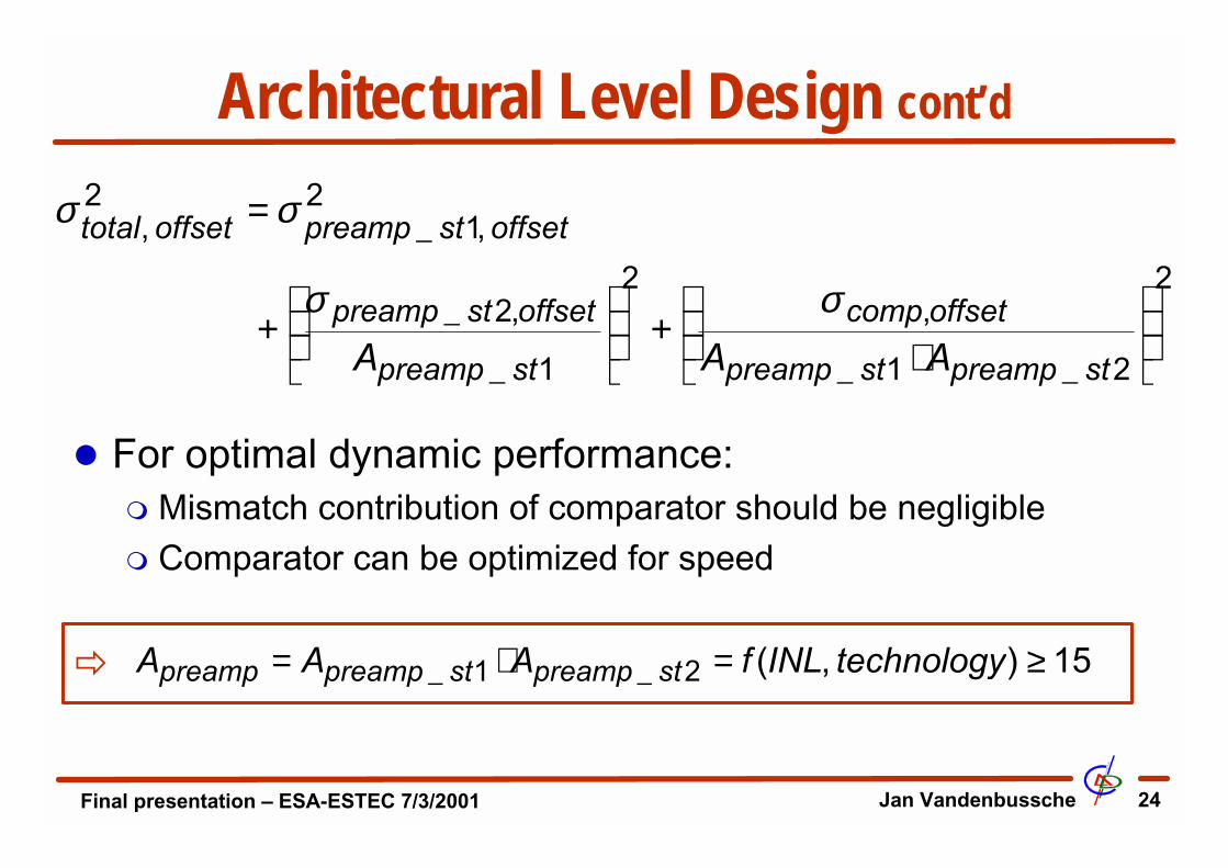
Architectural Level Design cont’d
2
2_1_
,2
1_
,2_
2,1_
2,
⋅
+
+
=
stpreampstpreamp
offsetcomp
stpreamp
offsetstpreamp
offsetstpreampoffsettotal
AAA
σσ
σσ
! For optimal dynamic performance:" Mismatch contribution of comparator should be negligible" Comparator can be optimized for speed
# 15),(2_1_ ≥=⋅= technologyINLfAAA stpreampstpreamppreamp

Final presentation – ESA-ESTEC 7/3/2001 Jan Vandenbussche 25
Architectural Level Design cont’d! Static performance! Dynamic
performance" Admissible phase
shift for Nyquistperformance?
" Vgs-Vt = 0.3 V" Preamplifier
Bandwith/InputFrequency = 5.
" 50dB 3rd orderdistortion (8bit)
# fp,preamp> 250MHz
°≈
≤ 1251
atanNyquistϕ
Final presentation – ESA-ESTEC 7/3/2001 Jan Vandenbussche 26
Design Methodology
Sizing Architectural level
? ?
?
?
?
Floorplanning
Layout Assembly & Verification
Synthesis:
Analog Digital
DESIGN PHASE
Sizing Device Level
Layout Device Level
Layout Module Level
Standard cell Place & route
- Matlab- Hspice
- Virtuoso
- Virtuoso- Mondriaan- C++
- Virtuoso
- Synopsis
- Cell Ensemble- Avant! P&R

Final presentation – ESA-ESTEC 7/3/2001 Jan Vandenbussche 27
Device Level Design: 1st preamp stage
1:1
1 : 21: 2 : 1 :1 1 : 21: 2 : 1 :1
1:1
m2a m2b
m1a m1b m1a m1b
m4a m4b m4c m4d
m33a m33d m33e m33hm3a m3b m3c m3d
m33a m33c m33f m33g
Vref_plus Vin_plus Vin_min Vref_min
Vbias_preamp_st1
Final presentation – ESA-ESTEC 7/3/2001 Jan Vandenbussche 28
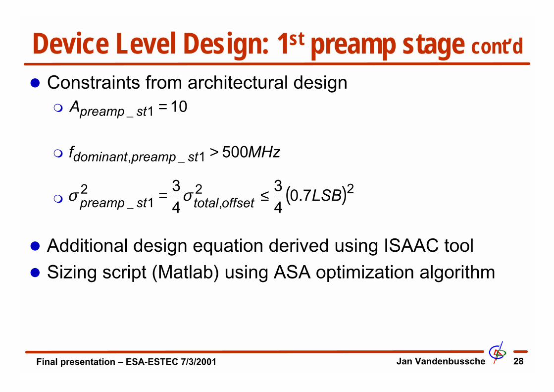
! Constraints from architectural design"
"
"
! Additional design equation derived using ISAAC tool! Sizing script (Matlab) using ASA optimization algorithm
Device Level Design: 1st preamp stage cont’d
101_ =stpreampA
MHzf stpreampdominant 5001_, >
( )22,
21_ 7.0
43
43
LSBoffsettotalstpreamp ≤= σσ

Final presentation – ESA-ESTEC 7/3/2001 Jan Vandenbussche 29
Device Level Design: 2nd preamp stage! Constraints from architectural level
"
"
"
! Additional design equation derived using ISAAC tool! Sizing script (Matlab) using ASA optimization algorithm
22_ =stpreampA
°≈
≤
>
1251
Arctan
5002_,
Nyquist
stpreampdominant MHzf
ϕ
( )2
2,
22_
7.04141
LSB
offsettotalstpreamp
≤
= σσ
m1a m1b
m2
Rload_a Rload_b
Vout_plus Vout_min
Vin_plus Vin_min
Vbias_preamp_st2

Final presentation – ESA-ESTEC 7/3/2001 Jan Vandenbussche 30
Device Level Design: comparator! very fast regenerative structure! reset when clock is high
Clk_comp
Vin
_plu
s_co
mp
Vin
_min
_co
mp
Ci+2 Clk_nand
Si
COMPARATOR NAND
M2
M1a M2b
M3a M3b
M4
M5a M5b
M6a M6b
M7a
M8a
M7b
M8b M9a M9b M9c M11b
M11b
M12aM10c
M10b
M10c
vbias_comp
nr1 nr2
Ci+1

Final presentation – ESA-ESTEC 7/3/2001 Jan Vandenbussche 31
Device Level Design: digital back-end! encodes the thermometer code in Gray code! 3- input NAND gate in the ROM decoder,
" additional error correction is done," avoid bubbles in the output" avoid metastability
! standard cell synthesis doesn’t meet high-speed specs" ‘manual’ design" Maple scripts for sizing" eldo for transistor level simulations

Final presentation – ESA-ESTEC 7/3/2001 Jan Vandenbussche 32
Layout generation! Layout-driven design: sized schematic alone does not
constitute an operational converter" analog and digital power supplies have been separated" around the perimeter of the chip 1 nF of decoupling capacitance
has been integrated to provide stable power supplies
! Layout preamplifier stages" layout of the preamplifiers was done manually" devices were generated using LAYLA" placement and routing was done manually" MONDRIAAN for regular arrays/connections" additional 500 pF of decoupling capacitance internally" guard rings to reduce substrate (digital) noise coupling

Final presentation – ESA-ESTEC 7/3/2001 Jan Vandenbussche 33
Layout generation cont’d

Final presentation – ESA-ESTEC 7/3/2001 Jan Vandenbussche 34
Layout generation cont’d! Comparator
" layout manually" placement & routing using Mondriaan for regular
arrays/connections

Final presentation – ESA-ESTEC 7/3/2001 Jan Vandenbussche 35
Layout generation cont’d! ROM decoder
" ROM cell manually" ROM array generated using the MONDRIAAN tool
! A buffered binary clock tree" clock tree generated using MONDRIAAN" the design and layout of the clock buffer was done manually

Final presentation – ESA-ESTEC 7/3/2001 Jan Vandenbussche 36
Layout generation cont’d

Final presentation – ESA-ESTEC 7/3/2001 Jan Vandenbussche 37
Layout: micro photograph
1st stage preamplifier
2nd stage preamplifier Gray decoder
S/H

Final presentation – ESA-ESTEC 7/3/2001 Jan Vandenbussche 38
Characterization High-speed ADC! Functional testing
" static measurements (INL/DNL)" dynamic Measurements (SFDR/SNDR)" datasheet
! Irradiation testing" budget reallocated for
redesign
! Dedicated test PCBwas developed

Final presentation – ESA-ESTEC 7/3/2001 Jan Vandenbussche 39
Characterization: static measurements! Full speed
measurement" fclk = 100 MS/s" fin = 3 kHz" calculate histogram" after unwrapping
INL/DNL can becalculated
! With defaultbiasing ADCshows missingcodes
! After tuning:DNL < 1.6 LSB
0 50 100 150 200 250-1.5
-1
-0.5
0
0.5
1
1.5
2
code []
DN
L [L
SB
]

Final presentation – ESA-ESTEC 7/3/2001 Jan Vandenbussche 40
Characterization: static measurements cont’d
0 50 100 150 200 250-3
-2
-1
0
1
2
code []
INL
[LS
B]
! After tuning:INL < 2.7 LSB

Final presentation – ESA-ESTEC 7/3/2001 Jan Vandenbussche 41
Characterization: dynamic measurements
! After tuning! fclk= 100MS/s! fin = 6 kHz
SFDR = 46 dBSNDR = 38 dB
-80
-60
-40
-20
0
20
40
Am
plit
ud
e [d
B]
10-4 10-3 10-2 10-1 100
frequency/fclk [ ]
SFDR
SNDR

Final presentation – ESA-ESTEC 7/3/2001 Jan Vandenbussche 42
Characterization: dynamic measurements cont’d
! After tuning! fclk= 100MS/s! fin = 5 MHz
SFDR = 42 dBSNDR = 29 dB
-80
-60
-40
-20
0
20
40
Am
plit
ud
e [d
B]
10-4 10-3 10-2 10-1 100
frequency/fclk []
SFDR
SNDR

Final presentation – ESA-ESTEC 7/3/2001 Jan Vandenbussche 43
Characterization: datasheetSpecification Target value First Design input capacitance < 100 pF 3 pF input range > 0.5 V ptp 1.3 V ptp latency not specified 1 clock cycle INL/DNL < ½ LSB 2.7/1.6 LSB SFDR > 45 dB 46 dB @ fin=6 kHz
42 dB @ fin=5 MHz SNDR > 40 dB 38 dB @ fin=6 kHz
29 dB @ fin=5 MHz ENOB 6.5 bits @ 30 MHz NM parallel output ok ok digital output:
• logic family • data format
CMOS levels Gray Code
CMOS levels Gray Code
Conversion rate 1 code/clock cycle 1 code/clock cycle Update rate 60 MS/s 100 MS/s Drive Capability - 10 pF@100MS/s
5 pF @200MS/s radiation tolerance 50 krad NM

Final presentation – ESA-ESTEC 7/3/2001 Jan Vandenbussche 44
Measurement analysis! High-speed ADC is working at 100 MS/s! Slightly out of spec! INL measurements show missing codes
105 110 115 120 125 130 135 140 145-1.5
-1
-0.5
0
0.5
1
1.5
code []
DN
L [L
SB
]
Codes are never excited

Final presentation – ESA-ESTEC 7/3/2001 Jan Vandenbussche 45
Measurement analysis cont’d! Malfunctioning second stage preamplifier
" common mode output 2nd stage preamp too low#input transistor of the comparator out of the saturation region#no gain in comparator#mismatch amplified instead of attenuated
! Hypothesis consolidated by:$additional (symbolic) analysis
comparator [Van der Plas ECCTD ‘98]
$ transistor level simulationwith tuned biasing
$measurements with tuned biasing:no more missing codes
m1a m1b
m2
Rload_a Rload_b
Vout_plus Vout_min
Vin_plus Vin_min
Vbias_preamp_st2

Final presentation – ESA-ESTEC 7/3/2001 Jan Vandenbussche 46
Measurement analysis: solutions! Possible solutions …
" increasing the DC current through the 2nd stage preamp$ current source diff pair no
longer in saturation!" isolating power supply 1st and
2nd stage preamp with FIB$ large setup times (days),
not routine job!$3 samples FIBed,
none were functional afterwards# Redesign?
m1a m1b
m2
Rload_a Rload_b
Vout_plus Vout_min
Vin_plus Vin_min
Vbias_preamp_st2

Final presentation – ESA-ESTEC 7/3/2001 Jan Vandenbussche 47
Measurement analysis: solutions cont’d

Final presentation – ESA-ESTEC 7/3/2001 Jan Vandenbussche 48
Redesign High-Speed ADC! New topology for 2nd stage! Comparator upscaled
" 1st design runs up to 200 MS/s!" lower mismatch
! Separate power supplyfor 1st and 2nd stagepreamplifiers
1 : 1 1 : 1
m2a
m1am1b
m3b m3cm3a m3d
vin_minvin_plus
vbias_st2

Final presentation – ESA-ESTEC 7/3/2001 Jan Vandenbussche 49
Redesign High-speed ADC cont’d
1st stage preamplifier
2nd stage preamplifier Gray decoder
S/H
Final presentation – ESA-ESTEC 7/3/2001 Jan Vandenbussche 50
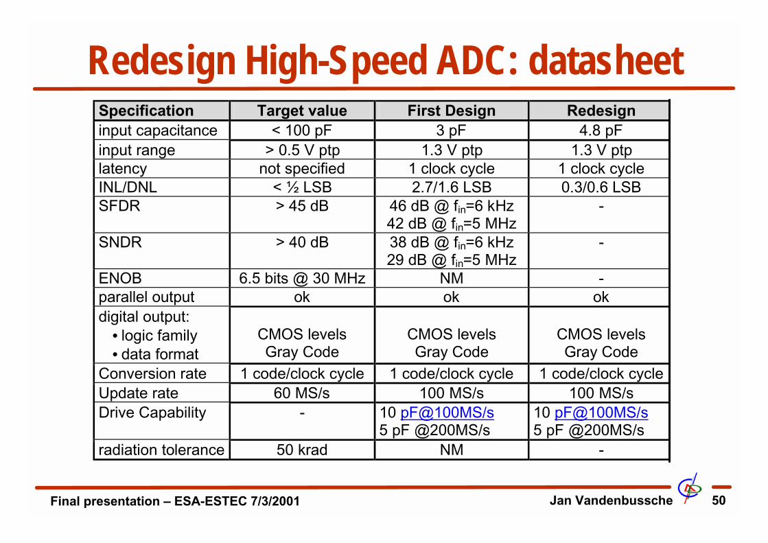
Redesign High-Speed ADC: datasheetSpecification Target value First Design Redesign input capacitance < 100 pF 3 pF 4.8 pF input range > 0.5 V ptp 1.3 V ptp 1.3 V ptp latency not specified 1 clock cycle 1 clock cycle INL/DNL < ½ LSB 2.7/1.6 LSB 0.3/0.6 LSB SFDR > 45 dB 46 dB @ fin=6 kHz
42 dB @ fin=5 MHz -
SNDR > 40 dB 38 dB @ fin=6 kHz 29 dB @ fin=5 MHz
-
ENOB 6.5 bits @ 30 MHz NM - parallel output ok ok ok digital output:
• logic family • data format
CMOS levels Gray Code
CMOS levels Gray Code
CMOS levels Gray Code
Conversion rate 1 code/clock cycle 1 code/clock cycle 1 code/clock cycle Update rate 60 MS/s 100 MS/s 100 MS/s Drive Capability - 10 pF@100MS/s
5 pF @200MS/s 10 pF@100MS/s 5 pF @200MS/s
radiation tolerance 50 krad NM -

Final presentation – ESA-ESTEC 7/3/2001 Jan Vandenbussche 51
Conclusions! Results
" high-speed 100MS/s 8-bit ADCcore (packaged/naked die)
" test PCB delivered
! ADC core was used as externalpart in WLAN prototype [IMEC]
! Publications

Final presentation – ESA-ESTEC 7/3/2001 Jan Vandenbussche 52
Publications! G. Van der Plas, J. Vandenbussche, G. Gielen and W. Sansen, "Mondriaan: a
Tool for Automated Layout Synthesis of Array-type Analog Blocks", Proc. on theIEEE 1998 Custom Integrated Circuits Conference, pp. 485-488, California, May1998.
! J. Vandenbussche, G. Van der Plas, W. Verhaegen and G. Gielen, "StatisticalBehavioral Modeling of A/D Converters", IEEE/VIUF International Workshop onBehavioral Modeling and Simulation, Florida, October 1998.
! G. Van der Plas, W. Daems, E. Lauwers, J. Vandenbussche, W. Verhaegen, G.Gielen, W. Sansen, "Symbolic Analysis of CMOS Regenerative Comparators",European Conference on Circuit Theory and Design, pp. 86-89, Italy, August1999.
! G. Van der Plas, J. Vandenbussche, W. Verhaegen, G. Gielen and W. Sansen,"Statistical Behavioral Modeling for A/D Converters", Proc. IEEE 1999International Conference on Electronics, Circuits and Systems, pp. 1713-1716,Cyprus, September 1999.


