22
Complete RF And Microwave Design Flow with AWR Design Environment Tabish Khan, AWR Corporation
| Date post: | 16-Jul-2018 |
| Category: |
Documents |
| Upload: | dangkhuong |
| View: | 280 times |
| Download: | 3 times |

Complete RF And Microwave Design Flow with AWR Design
Environment Tabish Khan, AWR Corporation
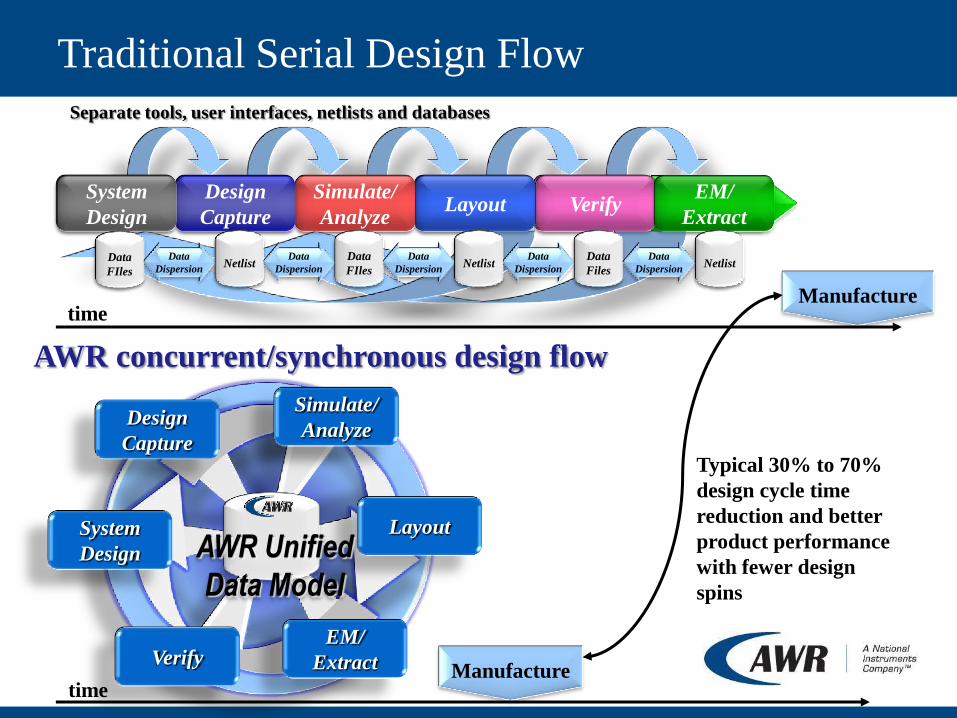
EM/
Extract Verify Layout
Simulate/
Analyze
Design
Capture
System
Design
Traditional Serial Design Flow
AWR concurrent/synchronous design flow
time
time Manufacture
Manufacture
Netlist Netlist Data
FIles Netlist
Data
Files
Typical 30% to 70%
design cycle time
reduction and better
product performance
with fewer design
spins
Data
Dispersion
Data
Dispersion
Data
Dispersion
Data
Dispersion
Verify Layout Simulate/
Analyze
Design
Capture
EM/
Extract
System
Design
Data
FIles
Data
Dispersion Netlist Netlist
Data
FIles Netlist
Data
Files
Data
FIles
Verify
Layout
Simulate/
Analyze Design
Capture
EM/
Extract
System
Design
Separate tools, user interfaces, netlists and databases
AWR Unified
Data Model

Microwave Office™
• Concurrent electrical/physical design
• Powerful circuit and EM simulation
• Fast tune, optimize, yield analysis
• RF aware layout
• MMIC design and layout
– GaAs, GaN, SiGe, foundry PDK’s
• Module design and layout
– MIC, LTCC, RF PCB
RF and Microwave Design Software

AWR Company Confidential
AWR’s EXTRACT Flow
Automates creation of
EM Documents:
Creates geometry from layout
Selects EM simulator of choice
Automatically adds ports
Sophisticated auto-mesh
Rapid design iterations
Reduce engineering overhead
Allows EM results to be seamlessly
included in any of the circuit
simulations that are supported by
the AWR Design Environment
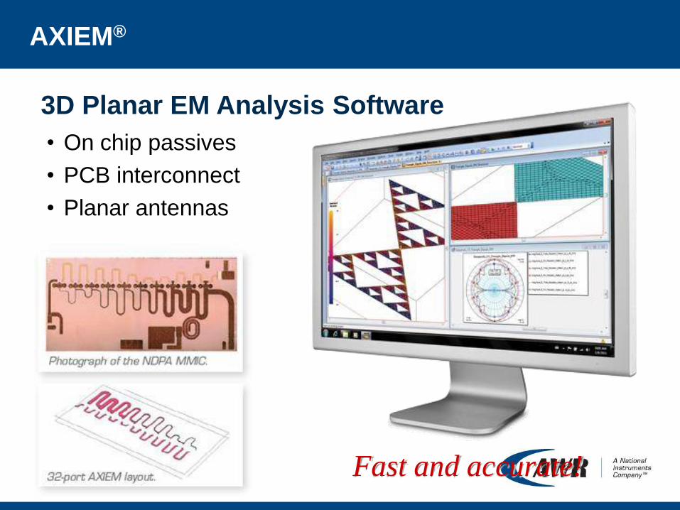
AXIEM®
• On chip passives
• PCB interconnect
• Planar antennas
3D Planar EM Analysis Software
Fast and accurate!
AWR Company Confidential
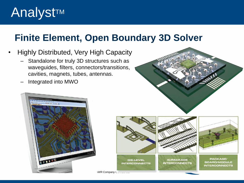
AnalystTM
• Highly Distributed, Very High Capacity
– Standalone for truly 3D structures such as
waveguides, filters, connectors/transitions,
cavities, magnets, tubes, antennas.
– Integrated into MWO
Finite Element, Open Boundary 3D Solver

RF Budget Cascade gain
Input/output IP3
Noise figure, etc.
RF Inspector Heritage tone inspector
to identify the cause of
an inter-modulation
product of an RF link
RF System End-to-End analysis
C/N, BER, ACPR, EVM, etc.
Circuit co-simulation
LabView co-simulation
Communication Standards WiMAX, IS2000, UWB, WCDMA
3GPP LTE, QAM, OQPSK, MPSK,
GSM EDGE, DVB, 802.11a/b/g, etc.
The most complete
RF system simulation
functionality in one
integrated tool
Visual System Simulator™ for RF System Simulation

AWR’s Visual System Simulator
• EDA Solution for Communications
Systems
• Mode’s include:
– Time Domain
– Complex Envelope
– Spur Analysis
• RF Link simulation includes…
– Amplifier, Mixer, Filter…
– Co-simulate with MWO circuits
– Co-simulate with hardware
• Measurements include
– Spectrum
– EVM
– Adjacent Channel Power
– Perform end-to-end simulations

LabVIEW VSS Co-simulation
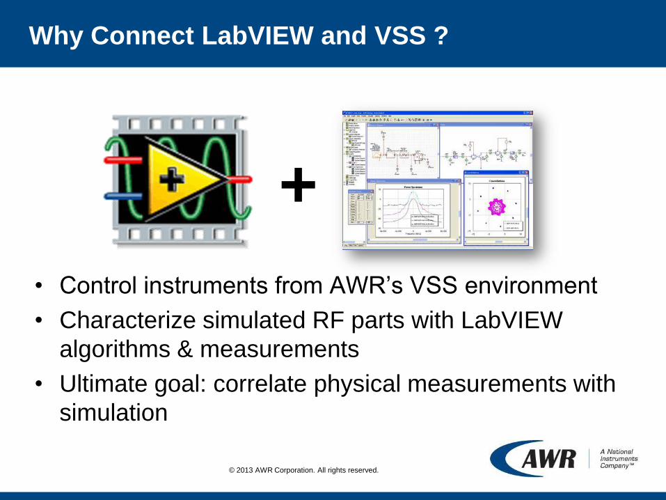
Why Connect LabVIEW and VSS ?
• Control instruments from AWR’s VSS environment
• Characterize simulated RF parts with LabVIEW
algorithms & measurements
• Ultimate goal: correlate physical measurements with
simulation
+
© 2013 AWR Corporation. All rights reserved.

Measurements in the Design Flow
Research/Modeling Design/Simulation Verification/Validation Manufacturing
Product Verification Design Verification
Measurements to
create models
“Hardware in the Loop” to
improve simulations Verification Test Production Test
© 2013 AWR Corporation. All rights reserved.

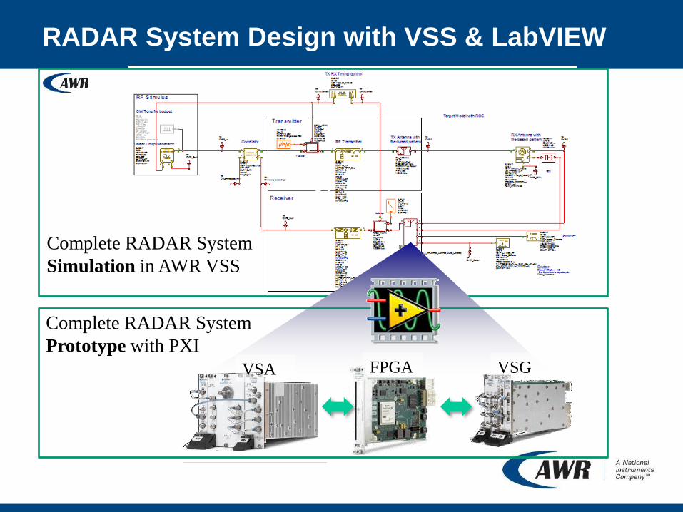
RADAR System Design with VSS & LabVIEW
Complete RADAR System
Simulation in AWR VSS
cv
Complete RADAR System
Prototype with PXI
cv FPGA VSG VSA
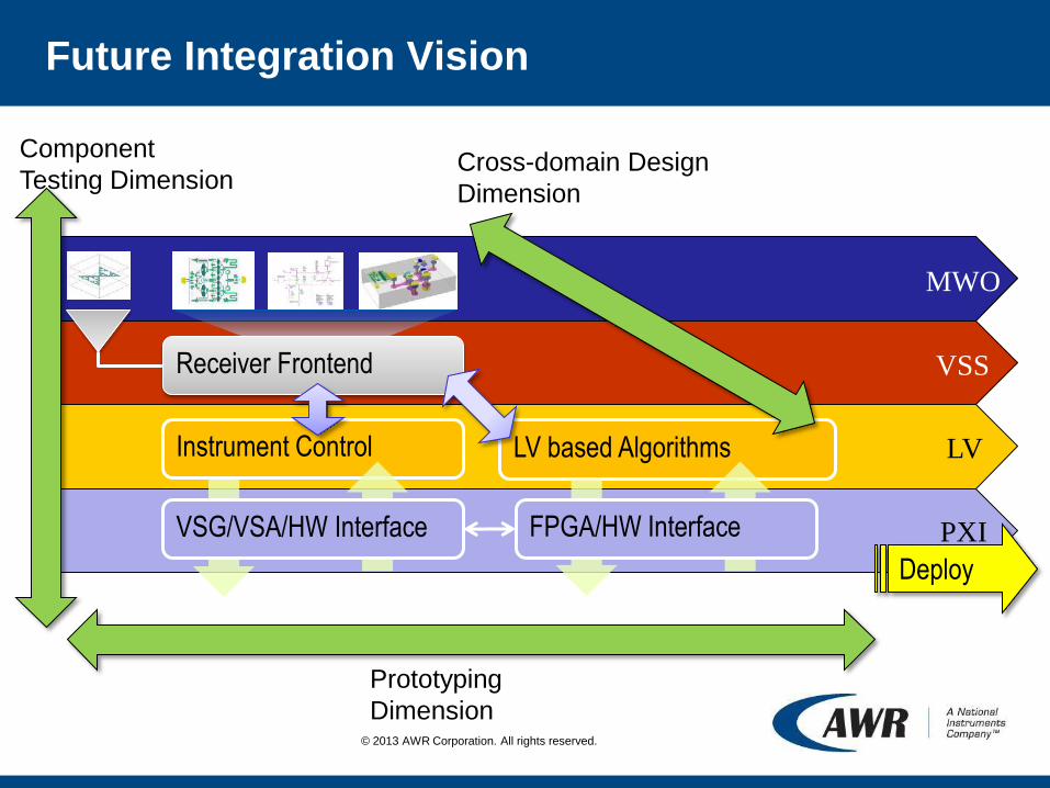
Future Integration Vision
LV based Algorithms
VSS
LV
MWO
PXI
Receiver Frontend
Instrument Control
FPGA/HW Interface
Component
Testing Dimension
Prototyping
Dimension
Cross-domain Design
Dimension
Deploy
VSG/VSA/HW Interface
© 2013 AWR Corporation. All rights reserved.
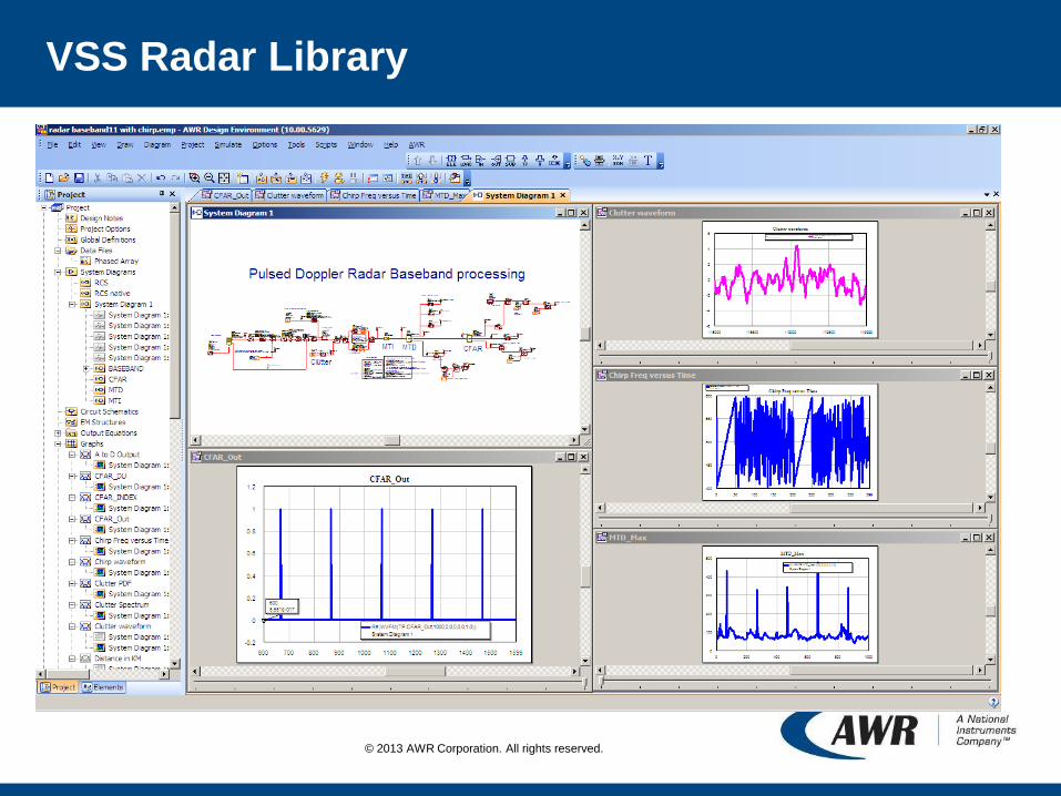
VSS Radar Library
© 2013 AWR Corporation. All rights reserved.
PORTDOUTPORTDIN AMP_B
1 2
NL_S
ISOLATOR
M_PROBE
BPFB
MMIC PA
340MHz
10MHz
8665MHz
9015MHz
Behavioral PA
or
BPFE BPFBBPFBBPFB AMP_BAMP_B
TP
TONETONE
IN OUT
LO
MIXER_B
IN OUT
LO
MIXER_B BPFE
AMP_B
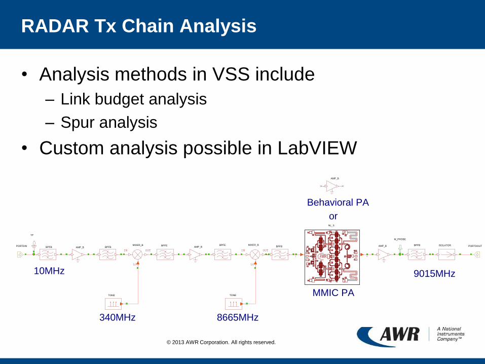
RADAR Tx Chain Analysis
• Analysis methods in VSS include
– Link budget analysis
– Spur analysis
• Custom analysis possible in LabVIEW
© 2013 AWR Corporation. All rights reserved.

RFB Cumulative Gain for TX
-20
0
20
40
60
S4\BPFB (F1) S4\AMP_B (A1) S4\BPFB (F2) S4\MIXER_B (Mixer1) S4\BPFE (F3) S4\AMP_B (A2) S4\BPFE (F4) S4\MIXER_B (Mixer2) S4\BPFB (F5) S4\AMP_B (A5) S4\AMP_B (A4) S4\BPFB (F6) S4\ISOLATOR (S8) TX_ANTENNA (S7)
p1
1459.54 dB
DB(C_GA(TP.Start,TP.Stop,1,0,1))[1]RFB Tx System
p1: Available Gain, Cumulative, dBFreq=9015 MHz
Link Budget Analysis
RFB C_NF for TX
0
1
2
3
4
5
S4\BPFB (F1) S4\AMP_B (A1) S4\BPFB (F2) S4\MIXER_B (Mixer1) S4\BPFE (F3) S4\AMP_B (A2) S4\BPFE (F4) S4\MIXER_B (Mixer2) S4\BPFB (F5) S4\AMP_B (A5) S4\AMP_B (A4) S4\BPFB (F6) S4\ISOLATOR (S8) TX_ANTENNA (S7)
p1
4.647 dB
DB(C_NF(TP.Start,TP.Stop,0,1,0,1))[1]
RFB Tx System
p1: Cascaded Noise Figure, Signal, Cumulative, dBFreq=9015 MHz
RFB Cumulative Gain for TX
-20
0
20
40
60
S4\BPFB (F1) S4\AMP_B (A1) S4\BPFB (F2) S4\MIXER_B (Mixer1) S4\BPFE (F3) S4\AMP_B (A2) S4\BPFE (F4) S4\MIXER_B (Mixer2) S4\BPFB (F5) S4\AMP_B (A5) S4\AMP_B (A4) S4\BPFB (F6) S4\ISOLATOR (S8) TX_ANTENNA (S7)
p1
1459.54 dB
DB(C_GA(TP.Start,TP.Stop,1,0,1))[1]RFB Tx System
p1: Available Gain, Cumulative, dBFreq=9015 MHz
-5000 0 5000 10000 15000 20000 25000 30000 35000 40000
Frequency (MHz)
RFI for TX
-400
-300
-200
-100
0
100
9015 MHz59.55 dBm
Results: – Cascaded NF
– Available Gain
– Spurs
Gain
Noise Figure
Spurs
© 2013 AWR Corporation. All rights reserved.

RADAR Antenna Models in VSS
RX antenna model can have multiple inputs to allow for interfering signals and/or
clutter
– THETA and PHI can be specified for Desired Signal, Jammer, Clutter,
etc….
– Corresponding gain and phase are picked off antenna pattern
Desired signal
& Clutter
Jammer
Multiple Theta Phi cuts
© 2013 AWR Corporation. All rights reserved.
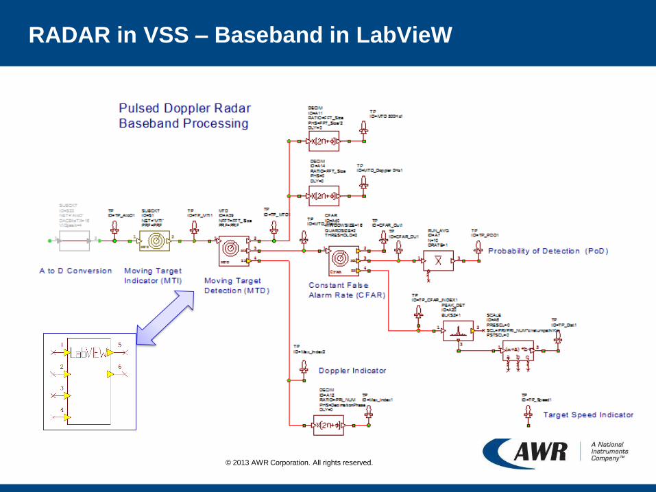
RADAR in VSS – Baseband in LabVieW
© 2013 AWR Corporation. All rights reserved.
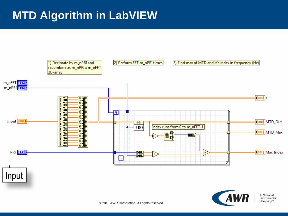
Input
MTD Algorithm in LabVIEW
© 2013 AWR Corporation. All rights reserved.

Example Output of MTD Algorithm
MIN RANGE VERSUS CLUTTER MIN RANGE VERSUS CLUTTER
© 2013 AWR Corporation. All rights reserved.
RADAR System Design with VSS & LabVIEW
Complete RADAR System
Simulation in AWR VSS
cv
Complete RADAR System
Prototype with PXI
cv FPGA VSG VSA

Learn More…
Online:
• www.awrcorp.com
• www.AWR.TV
Communities:
• YouTube
Email:


