I48 IEEE TRANSACTIONS ON EDUCATION, VOL. 36, NO. 1, FEBRUARY 1993 Computer Aided Engineering in Microelectronic Processes and Design in Singapore Vijay K. Arora, Senior Member, IEEE, and Ganesh S. Samudra, Member, IEEE Absfracf- With the complexity of megachips announced by several companies, the engineering of microelectronic processes and design will be impossible without the use of computers. An innovative approach for preparing engineering students in Sin- gapore by integrating computer aided engineering (CAE) skills in the laboratory environments is described in this paper. This integrative training is supported by use of simulation packages extensively used by industry worldwide. These packages allow students to simulate their processes enabling them to design an engineering experiment most likely to succeed. The use of word processing and graphics software available on PC’s and Mac’s spread all over the campus enhances their communication skills in preparing formal reports and presentations. The enhancement of technical and other liberal learning skills of the engineer- ing students by integrative teaching involving theory, computer simulation, and design is emphasized. I. INTRODUCTION N engineering the education for training engineers for the I industrial environments we are likely to face in the twenty- first century, computer aided engineering (CAE) plays a crucial role in understanding and designing complex electronic sys- tems [l]. Therefore, the computer has become a mandatory tool in academia and industry [2], [3]. A walk around the National University of Singapore (NUS) campus reveal%that there are as many computers as there are students, faculty and staff, put together. In recognition of these technological trends and the initiation of a national plan in the early 1980’s for promoting computer aided designicomputer aided engineering in training institutions in Singapore environments, NUS set up a CAD/CAM center with the availability of Sun, HP, and Intergraph workstations. In the late eighties, a computer based learning (CBL) center was established where networked Mac and PC clusters are available. These two sets of activities have an objective of promoting the use of computers in the Faculty of Engineering for educational purposes and eventual industrial applications. In Singapore, as anywhere else, the universities will be at the core of a layered network of socio-industrial systems. To understand this central layer, the students need to understand design, production, sales, and marketing with the help of a central database assisted by the use of networked computers. Manuscript received June 1992. V.K. Arora is with the Department of Electrical and Computer Engineering, Wilkes University, Wilkes-Barre, PA 18707. He is currently a Visiting Professor in the Department of Electrical Engineering, National University of Singapore, Singapore 051 1, G.S. Samudra is with the Department of Electrical Engineering, National University of Singapore, Singapore 051 1. IEEE Log Number 9202866. The evolving industrial patterns where multinational compa- nies control the global scene will necessitate our students to understand higher layers as well. These higher layers include societal needs, personnel, cultures, suppliers, finances, social factors, global environments, and legal issues. In this context, a working engineer or a student or an educator may find the use of international networks crucial to his survival in a competitive world to exchange information or share resources around the globe. This prompted the university to install bitnethternet a few years back. NUSnet, a local area network allows easy exchange of information between computers and with international networks. A NUS-Telecom masterplan for optical fiber subscriber network for the development of Sin- gapore’s telecommunications infrastructure has recently been launched in cooperation with Singapore Telecom. As the electrical engineering curriculum in Section I1 of this paper indicates, these issues are addressed in a four-year degree program accredited by IEE (U.K.). Singapore engineering studtnts enter the university with a solid technical background in the mathematical and physical sciences and students are hard working as they face the competitive environment. There- fore, it is easier for the faculty to assign them challenging assignments which involve the use of computers. In recent years, the Asia-Pacific region has been a focus of attention in the international arena as multinational companies are opening new operations because of an excellent infrastruc- ture and trained manpower coming out of the universities and polytechnics. Microelectronics has been defined as an area of strategic importance for the welfare of industry on the global economic scene. This is best exemplified by the newly created Institute of Microelectronics in Singapore. Other projects in this area include Japan’s VLSI project, USA’s Sematech VHSIC project, and the European JESSI project. The Ex- ploratory Research for Advanced Technology (ERATO) pro- gram of Japan Research and Development Corporation (JRDC) and Japan’s Ministry of International Trade and Industry are giving extensive support to the development in this area. Considering these developments which will be crucial to the survival of industry in microelectronics/nanoelectronics, we present here an approach for microelectronics process and design education. 11. ENGINEERING EDUCATION IN SINGAPORE Multinational companies are using Singapore as a vantage point for the Asia-Pacific region from where to oversee their regional operations, because of the high class infrastructure and trained manpower. These developments led government 0018-9359/93$03.00 0 1993 IEEE
Transcript
I48 IEEE TRANSACTIONS ON EDUCATION, VOL. 36, NO. 1, FEBRUARY 1993
Computer Aided Engineering in Microelectronic Processes and Design in Singapore
Vijay K. Arora, Senior Member, IEEE, and Ganesh S. Samudra, Member, IEEE
Absfracf- With the complexity of megachips announced by several companies, the engineering of microelectronic processes and design will be impossible without the use of computers. An innovative approach for preparing engineering students in Sin- gapore by integrating computer aided engineering (CAE) skills in the laboratory environments is described in this paper. This integrative training is supported by use of simulation packages extensively used by industry worldwide. These packages allow students to simulate their processes enabling them to design an engineering experiment most likely to succeed. The use of word processing and graphics software available on PC’s and Mac’s spread all over the campus enhances their communication skills in preparing formal reports and presentations. The enhancement of technical and other liberal learning skills of the engineer- ing students by integrative teaching involving theory, computer simulation, and design is emphasized.
I. INTRODUCTION N engineering the education for training engineers for the I industrial environments we are likely to face in the twenty-
first century, computer aided engineering (CAE) plays a crucial role in understanding and designing complex electronic sys- tems [l]. Therefore, the computer has become a mandatory tool in academia and industry [ 2 ] , [3]. A walk around the National University of Singapore (NUS) campus reveal% that there are as many computers as there are students, faculty and staff, put together. In recognition of these technological trends and the initiation of a national plan in the early 1980’s for promoting computer aided designicomputer aided engineering in training institutions in Singapore environments, NUS set up a CAD/CAM center with the availability of Sun, HP, and Intergraph workstations. In the late eighties, a computer based learning (CBL) center was established where networked Mac and PC clusters are available. These two sets of activities have an objective of promoting the use of computers in the Faculty of Engineering for educational purposes and eventual industrial applications.
In Singapore, as anywhere else, the universities will be at the core of a layered network of socio-industrial systems. To understand this central layer, the students need to understand design, production, sales, and marketing with the help of a central database assisted by the use of networked computers.
Manuscript received June 1992. V.K. Arora is with the Department of Electrical and Computer Engineering,
Wilkes University, Wilkes-Barre, PA 18707. He is currently a Visiting Professor in the Department of Electrical Engineering, National University of Singapore, Singapore 051 1,
G.S. Samudra is with the Department of Electrical Engineering, National University of Singapore, Singapore 051 1.
IEEE Log Number 9202866.
The evolving industrial patterns where multinational compa- nies control the global scene will necessitate our students to understand higher layers as well. These higher layers include societal needs, personnel, cultures, suppliers, finances, social factors, global environments, and legal issues. In this context, a working engineer or a student or an educator may find the use of international networks crucial to his survival in a competitive world to exchange information or share resources around the globe. This prompted the university to install bitnethternet a few years back. NUSnet, a local area network allows easy exchange of information between computers and with international networks. A NUS-Telecom masterplan for optical fiber subscriber network for the development of Sin- gapore’s telecommunications infrastructure has recently been launched in cooperation with Singapore Telecom. As the electrical engineering curriculum in Section I1 of this paper indicates, these issues are addressed in a four-year degree program accredited by IEE (U.K.). Singapore engineering studtnts enter the university with a solid technical background in the mathematical and physical sciences and students are hard working as they face the competitive environment. There- fore, it is easier for the faculty to assign them challenging assignments which involve the use of computers.
In recent years, the Asia-Pacific region has been a focus of attention in the international arena as multinational companies are opening new operations because of an excellent infrastruc- ture and trained manpower coming out of the universities and polytechnics. Microelectronics has been defined as an area of strategic importance for the welfare of industry on the global economic scene. This is best exemplified by the newly created Institute of Microelectronics in Singapore. Other projects in this area include Japan’s VLSI project, USA’s Sematech VHSIC project, and the European JESSI project. The Ex- ploratory Research for Advanced Technology (ERATO) pro- gram of Japan Research and Development Corporation (JRDC) and Japan’s Ministry of International Trade and Industry are giving extensive support to the development in this area. Considering these developments which will be crucial to the survival of industry in microelectronics/nanoelectronics, we present here an approach for microelectronics process and design education.
11. ENGINEERING EDUCATION IN SINGAPORE
Multinational companies are using Singapore as a vantage point for the Asia-Pacific region from where to oversee their regional operations, because of the high class infrastructure and trained manpower. These developments led government
0018-9359/93$03.00 0 1993 IEEE
I
IEEE TRANSACTIONS ON EDUCATION, VOL. 36, NO. I . FEBRUARY 1993 149
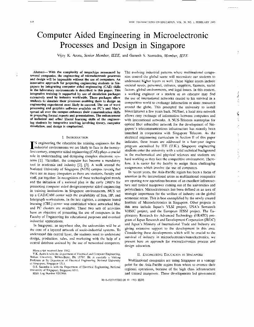
TABLE I UNDERGRADUATE COURSE STRUCTURE IN ELECTRICAL ENGINEERING AT NUS
First Year EGlOl Mathematics EG106 Engineering I1 EG102 Computing EG108 Physics EG103 Graphics EG 109 WorkshopiLaboratory EG104 Economics Technical Report Writing EG10.5 Engineering I
EE201 Mathematics €33202 Fields and Circuits EE203 Electronics I Technical Communications Skills EE208 Laboratory
EE301 Mathematics EE302 Electronics 11 EE303 Materials and Devices I1 EE304 Control and Machines
Optional courses (3 in each term): EE411 VLSI Circuits and Systems Design EE412 VLSI Fabrication Technology EE413 Optoelectronics EE421 Computer Architecture EE422 Real Time and Knowledge Based Systems EE423 Computer Networks EE431 Digital Communications EE432 Microwaves EE461 Systems Engineering EE433 Optical Fibre Communications
Second Year EG201 Financial Accounting EE204 Digital Systems EE20.5 Computing Science I EE206 Electrical Machines EE207 Materials and Devices I
Third Year EG301 Sociology EE305 Microcomputer Systems EE306 Computing Science 11 EE 307 Communications EE 308 Laboratory and Projects
Fourth Year EG401 Management and Law EE400 Laboratory and Projects
EE441 Control Systems I EE442 Control Systems I1 EE443 Robotics and Vision EE444 Signal Processing EE451 Power Semiconductor Drives EE4.52 Power Systems Analysis and Protection EE453 Power Systems Dynamics and Control
to put resources in the universities which will supply the projected manpower needs of the nation. In addition to NUS, Nanyang Technological University and four polytechnics sup- port the effort of producing trained manpower. A number of institutes and research centers have been created with the intention of quick transfer of technology from conception to manufacturing stage.
The Faculty of Engineering is one of the eight faculties in NUS with a student intake of approximately 500 in the first (Freshmen) year of a four-year degree program leading to the Bachelor of Engineering (B. Eng.) degree. With Singapore rapidly progressing up the technology ladder, the faculty has made available the opportunities for higher degrees. The faculty offers part-time and full-time evening courses leading to the M. Sc. degree and facilities for research leading to the M. Eng. and Ph. D. degrees. Considering the need for technology management, a Master’s degree in technology management in association with the Faculty of Business Administration has recently been announced.
The department of electrical engineering offers a rich and varied undergraduate program lasting four years, of which the first three years of the program are broadbased and provide a firm grounding in the fundamentals of electrical engineering. In the fourth and final year, the students are given opportunities to specialize. Optional subjects deal with state-of-the-art topics in areas such as VLSI technology, semi- conductor lasers and optoelectronics, computer architectures, advanced control techniques,‘knowledge-based systems, com- puter networks, optical fiber communications, computer vision, robotics, and power electronics. These topics involve computer usage. To ensure that the program is always up-to-date, the department constantly monitors the current trends and modifies the curriculum accordingly to reflect any major shifts arising from technological advances.
In addition to the fundamental courses listed in Table I, the students have set laboratory experiments (including computer interfacing and software) for 260 hours, miniprojects for about 80 hours, and final year R&D projects for about 225 hours. For the projects, they have to write a thesis-like comprehensive report. They also have several courses in humanities and management to improve their communication and interpersonal skills.
111. CAE IN DEVICE MODELING No doubt CAE will be a pervasive technology without
which it will be impossible to educate our students in the coming years. A pervasive technology is more noticeable by its absence than its presence, in just the way that automobiles, televisions, and telephones are in our society [4]. We, the educators in microelectronics, do not know how we will be able to teach our students if we are asked not to use computers. Trial and errors in microelectronics experiments will waste expensive supplies in repeated trials to arrive at a successful one, creating an atmosphere where such laboratories will be used only for specialized purposes where the process is well understood. Certainly, such an approach will inhibit innovations. A careful planning by CAE will most likely lead to a successful experiment, thereby tremendously saving laboratory costs.
The training in microelectronics processes starts with a basic course in semiconductor devices. In NUS’s electrical engineering program, EE207: Materials and Devices I and EE303: Materials and Devices 11, teach fundamental device concepts. Both these courses make use of the textbooks listed in [5 ] - [7 ] . In the spirit of simplification, these text- books assume electronic devices of long length (the length being much larger than the diffusion length of minority car-
150 IEEE TRANSACTIONS ON EDUCATION, VOL. 36, NO. 1, FEBRUARY 1993
riers). Most of these long-length device mathematical models on current-voltage and capacitance-voltage characteristics fail very badly when applied for characterizing the miniaturized devices.
An example of a miniaturized device is the minority carriers profiles in scaled down dimensions of a diode [8]. When the bias is applied, the boundaries between the depletion and neutral layers will undoubtedly change, resulting in a change of the width of the neutral layers which may reduce to zero resulting in the punch-through phenomenon. This change in the width of neutral layers substantially changes the device behavior in the micro-world of fabricated devices. It is well known that the typical junction depth of a fabricated diode in the laboratory is only a few microns (1 micron (pm) =
m). Therefore, the simplified models (assuming long diodes) quoted in undergraduate textbooks do not depict the experimental reality. Even for long-diode behavior, the design of diode characteristics is difficult to implement, as suggested by Goel and Cobb [9]. By defining CAE projects which will analyze these models using the realistic few micron lengths of the diode regions enhances the students’ appreciation of the micro world in which electrons are likely to diffuse. The same is true of the bipolar junction transistors (BJT’s). The third year students at NUS study the bipolar devices in detail using PC-1D, a one-dimensional device simulator from the University of Iowa. The overview of a typical BJT microfabrication process is shown in Fig. 1, with the aid of device cross sections and layout. The fabrication process is simulated with SUPREM3 (a trademark of Technology Mod- eling Associates) to generate a BJT profile as shown in Fig. 2. The data obtained serves as input to a device simulator. After solving the standard device equations (Poisson’s and current continuity equations) numerically, PC-1D displays potkntial carrier concentration and other physical quantities throughout the depth of the device. This enables the students to study in detail the minority carrier and electric field distributions in the base of the BJT, which play a crucial rule in the performance of the BJT. One can engineer a better BJT with the help of SUPREM and PC-1D by altering base dopings and base widths.
The above device modeling exercises allow extraction of the internal device parameters (including parasitic capacitances and resistances) from the physics of these devices. These parameters can be then input into SPICE, a circuit simulator from the University of California at Berkeley, to get the terminal characteristics of the discrete devices and systems of discrete devices. Such exercises are extremely useful in developing their skills in the world of humans and machines. They learn to do teamwork, prepare to teach each other and in general set a dialog which is beneficial to the student community [lo]. Above all, they bring the excitements of the new findings or capabilities of a new software to the teacher’s attention, thereby giving a crucial feedback to the teacher in designing innovative projects for next year’s class.
To enhance the communication skills of students, the stu- dents prepare a formal document by integrating engineer- ing and nonengineering factors. Many of our students have shown that our traditional way of presenting information
/ I
t I
I -- 1-1 I I I ~
I I
I !
(c)
j
I I , I
Fig. 1. Stages of bipolar cross-section and layout: (a) base diffusion, (b) emitter diffusion with base diffusion, (c) emitter and base contacts, and (d) metallization covering the contacts.
using viewgraphs is obsolete by using animation graphics effectively. This way not only have they learned the meaning of abstract mathematical equations for design purposes, but also have created an atmosphere of excitement where their active learning proved of immense educational value to peers and teachers alike.
IV. PROJECTORIENTED CAE
The projects assigned in the final year or in the courses
simulation of discrete devices, simulation of fabrication process, layout of various levels of chip geometries (mask layout), simulation of VLSI circuit performance, simulation of reliability and circuit failure as chips age, simulation of heat transport in chip packages,
involve one or more of the following activities:
I
IEEE TRANSACTIONS ON EDUCATION, VOL. 36, NO. I , FEBRUARY 1993
Bipolar Transistor P r o f i l e
I
1 1
U 15j ~ * t 1 ~ base width ‘- I 00
D;srance IllLcronsi 2.00
Fig. 2. Graphical output of the final profiles of bipolar process indicating the basewidth hetween-the two junctions. Such profiles are generated at each step during the simulation process.
simulation of industrial environments including plant lay- out, time behavior between various work areas, and automation, and technology management including integrated databases, planning, design, control, computer networking, and com- munication.
Examples of projects completed utilizing CAE tools exten-
design of an oversampling digital filter for Analog to
design of a digital audio-tone control unit, optimization of Lightly-Doped Drain (LDD) structure using MINIMOS, a 2-D Metal-Oxide-Semiconductor De- vice Simulator, developed at the Technical University of Vienna, Numerical simulation of heterostructure devices, and investigation of BJT properties with BAMBI, a 2-D gen- eral purpose device simulator, developed at the Technical University of Vienna.
The department offers a design elective EE411 for final year undergraduate students. In this course, the students extensively use the layout editor MAGIC, developed at University of California at Berkeley and associated logic simulator ESIM to design a cell of their choice. The students are given the option to design an adder, a barrel shifter or a multiplier, depending on their interests. Finally, students submit a formal report describing their approach to design, circuit layout and ESIM output.
NUS has a tradition of project presentation by final year (senior) students at the end of the second term (semester) before the faculty. A large number of projects have necessarily involved students who were successful in integrating CAE with engineering equipment.
sively are given below:
Digital Converter (ADC),
151
V. CONCLUSIONS
The use of CAE software to integrate engineering design skills with experimental skills greatly enhanced the value of microelectronics education for our students. These soft- ware tools have allowed engineering students to design and simulate complex microelectronic systems, without which it will be impossible to study such systems. This “learn and apply” approach taught them to learn facts in the context of synthesis, involving manpower, computer power, money power, knowledge power, etc., to produce a desired result. It created an environment of easy communication with design centers and production centers via networks. It has allowed them to prepare persuasive reports, documents, and computer aided presentations. Above all, this integrative learning has considerably enhanced the value of their engineering education by teamwork and data sharing. CAE training has made our students more communicative, expressive, respectful of peers’ work, and cooperative in the use of design software and other technical equipment.
ACKNOWLEDGMENTS
G. Samudra would like to acknowledge the useful conver- sations he had with the members of the faculty at NUS and V. Arora would like to thank NUS for its hospitality.
REFERENCES
In Procs. National S a . Tech. Conf., NSTB, Singapore, Sept., 1991,
C. Arms, Ed., Campus Networking Strategies. New York: Digital Press, 1988. A. S. Tenenbaum, Computer Networks, 2nd ed. Englewood Cliffs, NJ: Prentice-Hall, 1989. I. S. Birnbaum, “Computing in the 90’s: Implication for industry and society,” see reference [l], p. 7. S. M. Sze, Semiconductor Devices: Physics and Technology. New York: Wiley. 1985. G. W. Neudeck and R. F. Pierret, Eds., Modular Series on Solid State Devices. New York: Addison-Wesley. Ben Streetman, Solid State Electronic Devices. Englewood Cliffs, NJ: Prentice-Hall, 1990. M. S. Tyagi, Semiconductor Materials and Devices. Englewood Cliffs, NJ: Prentice-Hall, 1990. A. K. Goel and M. D. Cobb, “Innovative Analysis of Semiconductor Junctions using Personal Computer,” Int. J . Appl. Eng. Educ., vol. 7, pp. 71-75, 1991. V. Arora and V. Choudhry, “Integration of liberal learning skills with engineering design skills in the microelectronic fabrication, Int. J. Appl. Eng. Educ., vol. 7, no. 3, pp. 231-236, 1991.
pp. 10-11.
Vijay K. Arora (S’74-A’76-M’82-SM’86) re- ceived the Ph.D. degree from the University of Colorado, Boulder, CO, in 1973.
Having spent a year at the University of Colorado as a Postdoctoral Associate and Lecturer, he joined Western Michigan University Kalamazoo, MI, as an Assistant Professor, in August 1974. In September 1976, he moved to King Saud University in the Kingdom of Saudi Arabia as an Assistant Professor and was quickly promoted to Associate Professor and Professor. There, he provided consulting ser-
152 IEEE TRANSACTIONS ON EDUCATION. VOL. 36, NO. I , FEBRUARY 1993
vices in organization development and for teaching programs in colleges of engineering, medicine, science, and graduate studies. He was on sabbatical leave at the University of Illinois Urbana, IL, and the Illinois Institute of Technology Chicago, IL, during the academic year of 1981-1982. In August 1985, he joined Wilkes University, Wilkes-Barre, PA, where he is currently a Professor of Electrical Engineering. He is presently studying mobility limiting mechanisms in high-speed devices, including quantum and high- field effects. He has visited several international institutions and enjoys the privilege of knowing the cultures and educational methods being practiced around the globe. He participated in the Sakaki Quantum Wave Project involving the design of Quantum Well Wire FET‘s at the University of Tokyo under the Exploratory Research for Advanced Technology (ERATO) Program. Presently, he is a Visiting Professor at the National University of Singapore.
Dr. Arora is a member of several professional societies including APS, ASEE, Sigma-XI, IPA, AGS. He is listed in American Men and Women of Science and Who’s Who in Science and Engineering.
4
.
Ganesh S. Samudra (M’87) was born in India. He received the MSc. from Indian Institute of Technology, Bombay, India in 1976, and the M.S., M.S.E.E., and Ph.D. degrees from Purdue University, Lafayette, IN.
In 1985, he joined Texas Instruments, Inc., Dallas, TX, where he worked on development and support of semiconductor process and device simulation tools. In 1987, he joined Texas Instruments, Bangalore, India, where he was section manager for simulation. He was elected Member of Grow
Technical Staff, in 1988, for outstanding technical contributions in simulation. Since 1989, he has been with the Department of Electrical Engineering, National University of Singapore, Singapore, where he is presently a Senior Lecturer. He is currently working in Technology and Design CAD tools.
Dr. Samudra i s Chairman of IEEE Circuits and System Chapter of Singapore.
‘leaching k’irmware as a Bridge Between Hardware and Software
Daniel Mange,
Abstract-The Electrical Engineering Department of the Swiss Federal Institute of Technology in Lausanne, Switzerland, has recently introduced a new course for freshmen aimed to tie together both sides of computer science (hardware, such as logic and digital systems, and software, such as classic procedural PASCAL programming), to emphasize systematic and invariant methods rather than describing rapidly changing technologies and to give a faster and stronger introduction to the profession.
This one-year course (with labs) is called an Introduction to firmware theory, the term firmware being comprehended as the art and the technique of transforming hardware (logic systems) into software (programs) and vice versa; the entire course is based on the central idea of equivalence between hardware and software which is exhibited by means of one preferred repre- sentation, the binary decision tree. In this paper, a very simple example is used to show the definition of a binary decision tree, its simplification and its decomposition. Hardware implementation is illustrated by a demultiplexer network, while software imple- mentation is highlighted by the use of two structured languages: a high-level language called MICROPASCAL and a low-level language called U, the latter being obtained by a compilation of the former. The conclusion gives a summary of the course, including laboratory sessions, as it is taught at present.
I. INTRODUCTION number of American institutions (Drexel University in A Philadelphia, Rose-Hulman Institute of Technology in
Terre Haute, Indiana, and Texas A & M University) are trying experiments for restructuring their curricula for freshmen and sophomores and are searching for a “magic ingredient” that could give engineering instructors the incentive to design, develop, and test innovative approaches to undergraduate education [l].
Manuscript received September 1992. The author is with the Logic Systems Laboratory, The Swiss Federal
IEEE Log Number 9205770. Institute of Technology, CH 1015 Lausanne, Switzerland.
Member, IEEE
In the particular area of computer science, the Electrical Engineering Department of the Swiss Federal Institute of Technology in Lausanne, Switzerland has faced the same challenge and has decided to introduce in 1988 a new course for freshmen (first year) aimed to:
give a faster and stronger introduction to the profession; tie together both sides of computer science: hardware (logic and digital systems) and software (classic proce- dural programming such as PASCAL); and emphasize systematic and (almost) invariant methods rather than describing fast changing present technologies.
The solution arrived at consists of a one-year course (with laboratory experiments) dedicated to an Introduction to firmware theory, the term firmware being compre- hended as the a r t and the technique of transforming hardware (logic systems) into software (programs) and vice versa.
The entire course is therefore based on the central idea of equivalence between hardware and software; and this equivalence, which at the mathematical level rests on the concept of the algorithm, is exhibited by means of one preferred representation, the binary decision tree. In this paper, a very simple example (a decoder designed for an electronic watch) is used to show the definition of a binary decision tree, its simplification (Section 11) and its decomposition (Section 111). Hardware implementation is illustrated by a demultiplexer network (Section IV), while software implementation is highlighted by the use of two structured languages: a high-level language called MICROPASCAL and a low-level language called L4 (Section V). The conclusion gives a summary of the course, as it is taught at present at the Swiss Federal Institute of Technology.