43
1 Copyright © 2012, Elsevier Inc. All rights reserved. Chapter 4 Data-Level Parallelism in Vector, SIMD, and GPU Architectures Computer Architecture A Quantitative Approach, Fifth Edition

1Copyright © 2012, Elsevier Inc. All rights reserved.
Chapter 4
Data-Level Parallelism in Vector, SIMD, and GPU Architectures
Computer ArchitectureA Quantitative Approach, Fifth Edition

2Copyright © 2012, Elsevier Inc. All rights reserved.
Introduction
SIMD architectures can exploit significant data- level parallelism for:
matrix-oriented scientific computing
media-oriented image and sound processors
SIMD is more energy efficient than MIMD
Only needs to fetch one instruction per data operation
Makes SIMD attractive for personal mobile devices
SIMD allows programmer to continue to think sequentially
Introduction

3Copyright © 2012, Elsevier Inc. All rights reserved.
SIMD Parallelism
Vector architectures
SIMD extensions
Graphics Processor Units (GPUs)
For x86 processors:
Expect two additional cores per chip per year
SIMD width to double every four years
Potential speedup from SIMD to be twice that from MIMD!
Introduction

4Copyright © 2012, Elsevier Inc. All rights reserved.
Vector Architectures
Basic idea:
Read sets of data elements into “vector registers”
Operate on those registers
Disperse the results back into memory
Registers are controlled by compiler
Used to hide memory latency
Leverage memory bandwidth
Vector A
rchitectures

5Copyright © 2012, Elsevier Inc. All rights reserved.
VMIPS
Example architecture: VMIPS
Loosely based on Cray-1
Vector registers
Each register holds a 64-element, 64 bits/element vector
Register file has 16 read ports and 8 write ports
Vector functional units
Fully pipelined
Data and control hazards are detected
Vector load-store unit
Fully pipelined
One word per clock cycle after initial latency
Scalar registers
32 general-purpose registers
32 floating-point registers
Vector A
rchitectures

6Copyright © 2012, Elsevier Inc. All rights reserved.
VMIPS Instructions
ADDVV.D: add two vectors
ADDVS.D: add vector to a scalar
LV/SV: vector load and vector store from address
Example: DAXPYL.D
F0,a
; load scalar a
LV
V1,Rx
; load vector XMULVS.D
V2,V1,F0
; vector-scalar multiply
LV
V3,Ry
; load vector YADDVV
V4,V2,V3
; add
SV
Ry,V4
; store the result
Requires 6 instructions vs. almost 600 for MIPS
Vector A
rchitectures

7Copyright © 2012, Elsevier Inc. All rights reserved.
Vector Execution Time
Execution time depends on three factors:
Length of operand vectors
Structural hazards
Data dependencies
VMIPS functional units consume one element per clock cycle
Execution time is approximately the vector length
Convey
Set of vector instructions that could potentially execute together
Vector A
rchitectures

8Copyright © 2012, Elsevier Inc. All rights reserved.
Chimes
Sequences with read-after-write dependency hazards can be in the same convey via chaining
Chaining
Allows a vector operation to start as soon as the individual elements of its vector source operand become available
Chime
Unit of time to execute one convey
m conveys executes in m chimes
For vector length of n, requires m x n clock cycles
Vector A
rchitectures
9Copyright © 2012, Elsevier Inc. All rights reserved.
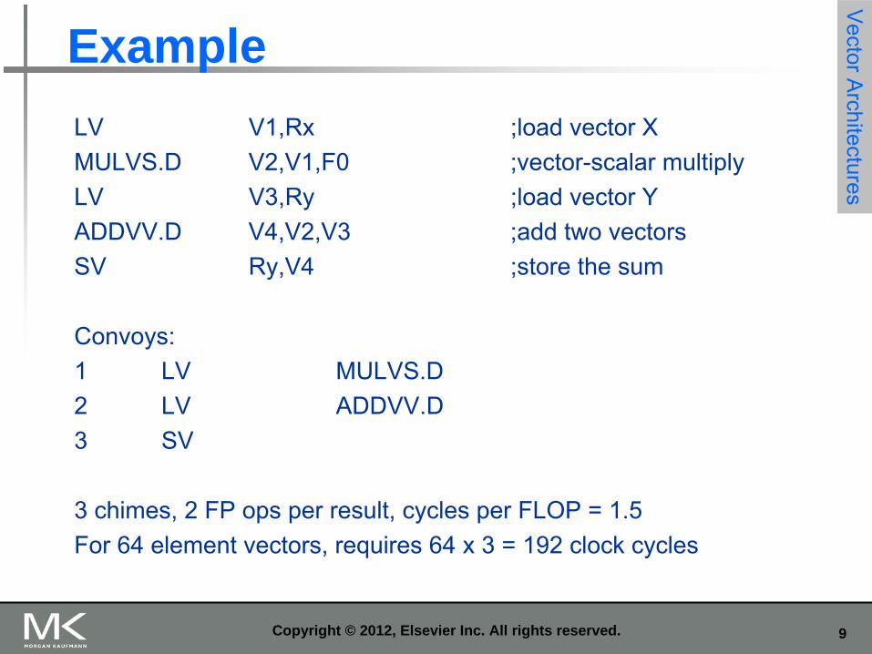
ExampleLV
V1,Rx
;load vector XMULVS.D
V2,V1,F0
;vector-scalar multiplyLV
V3,Ry
;load vector YADDVV.D
V4,V2,V3
;add two vectorsSV
Ry,V4
;store the sum
Convoys:1 LV
MULVS.D2
LV
ADDVV.D3 SV
3 chimes, 2 FP ops per result, cycles per FLOP = 1.5For 64 element vectors, requires 64 x 3 = 192 clock cycles
Vector A
rchitectures

10Copyright © 2012, Elsevier Inc. All rights reserved.
Challenges
Start up time
Latency of vector functional unit
Assume the same as Cray-1
Floating-point add => 6 clock cycles
Floating-point multiply => 7 clock cycles
Floating-point divide => 20 clock cycles
Vector load => 12 clock cycles
Improvements:
> 1 element per clock cycle
Non-64 wide vectors
IF statements in vector code
Memory system optimizations to support vector processors
Multiple dimensional matrices
Sparse matrices
Programming a vector computer
Vector A
rchitectures

11Copyright © 2012, Elsevier Inc. All rights reserved.
Multiple Lanes
Element n of vector register A is “hardwired”
to element n of vector register B
Allows for multiple hardware lanes
Vector A
rchitectures

12Copyright © 2012, Elsevier Inc. All rights reserved.
Vector Length Register
Vector length not known at compile time?
Use Vector Length Register (VLR)
Use strip mining for vectors over the maximum length:low = 0;VL = (n % MVL); /*find odd-size piece using modulo op % */for (j = 0; j <= (n/MVL); j=j+1) { /*outer loop*/
for (i = low; i < (low+VL); i=i+1) /*runs for length VL*/Y[i] = a * X[i] + Y[i] ; /*main operation*/
low = low + VL; /*start of next vector*/VL = MVL; /*reset the length to maximum vector length*/
}
Vector A
rchitectures

13Copyright © 2012, Elsevier Inc. All rights reserved.
Vector Mask Registers
Consider:for (i = 0; i < 64; i=i+1)
if (X[i] != 0)X[i] = X[i] –
Y[i];
Use vector mask register to “disable”
elements:LV
V1,Rx
;load vector X into V1LV
V2,Ry
;load vector YL.D
F0,#0
;load FP zero into F0SNEVS.D
V1,F0
;sets VM(i) to 1 if V1(i)!=F0SUBVV.D
V1,V1,V2
;subtract under vector maskSV
Rx,V1
;store the result in X
GFLOPS rate decreases!
Vector A
rchitectures

14Copyright © 2012, Elsevier Inc. All rights reserved.
Memory Banks
Memory system must be designed to support high bandwidth for vector loads and stores
Spread accesses across multiple banks
Control bank addresses independently
Load or store non sequential words
Support multiple vector processors sharing the same memory
Example:
32 processors, each generating 4 loads and 2 stores/cycle
Processor cycle time is 2.167 ns, SRAM cycle time is 15 ns
How many memory banks needed?
Vector A
rchitectures

15Copyright © 2012, Elsevier Inc. All rights reserved.
Stride
Consider:for (i = 0; i < 100; i=i+1)
for (j = 0; j < 100; j=j+1) {A[i][j] = 0.0;for (k = 0; k < 100; k=k+1)A[i][j] = A[i][j] + B[i][k] * D[k][j];
}
Must vectorize multiplication of rows of B with columns of D
Use non-unit stride
Bank conflict (stall) occurs when the same bank is hit faster than bank busy time:
#banks / LCM(stride,#banks) < bank busy time
Vector A
rchitectures

16Copyright © 2012, Elsevier Inc. All rights reserved.
Scatter-Gather
Consider:for (i = 0; i < n; i=i+1)
A[K[i]] = A[K[i]] + C[M[i]];
Use index vector:LV
Vk, Rk
;load K
LVI
Va, (Ra+Vk)
;load A[K[]]LV
Vm, Rm
;load M
LVI
Vc, (Rc+Vm)
;load C[M[]]ADDVV.D
Va, Va, Vc
;add them
SVI
(Ra+Vk), Va
;store A[K[]]
Vector A
rchitectures
17Copyright © 2012, Elsevier Inc. All rights reserved.
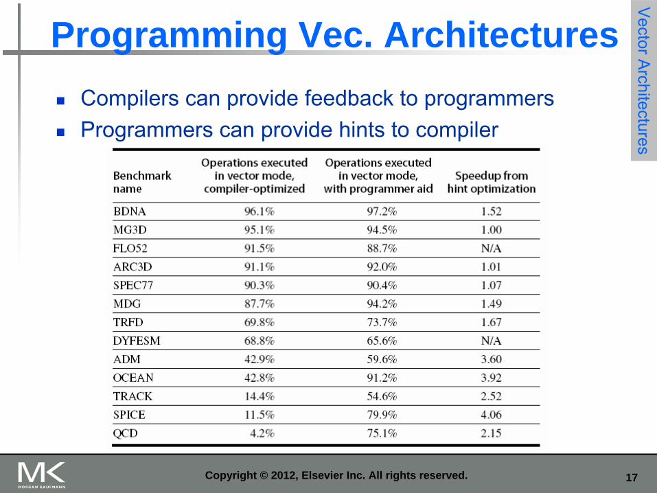
Programming Vec. Architectures
Compilers can provide feedback to programmers
Programmers can provide hints to compiler
Vector A
rchitectures

18Copyright © 2012, Elsevier Inc. All rights reserved.
SIMD Extensions
Media applications operate on data types narrower than the native word size
Example: disconnect carry chains to “partition”
adder
Limitations, compared to vector instructions:
Number of data operands encoded into op code
No sophisticated addressing modes (strided, scatter- gather)
No mask registers
SIM
D Instruction S
et Extensions for M
ultimedia

19Copyright © 2012, Elsevier Inc. All rights reserved.
SIMD Implementations
Implementations:
Intel MMX (1996)
Eight 8-bit integer ops or four 16-bit integer ops
Streaming SIMD Extensions (SSE) (1999)
Eight 16-bit integer ops
Four 32-bit integer/fp ops or two 64-bit integer/fp ops
Advanced Vector Extensions (2010)
Four 64-bit integer/fp ops
Operands must be consecutive and aligned memory locations
SIM
D Instruction S
et Extensions for M
ultimedia

20Copyright © 2012, Elsevier Inc. All rights reserved.
Example SIMD Code
Example DXPY:L.D
F0,a
;load scalar aMOV
F1, F0
;copy a into F1 for SIMD MULMOV
F2, F0
;copy a into F2 for SIMD MULMOV
F3, F0
;copy a into F3 for SIMD MULDADDIU
R4,Rx,#512
;last address to loadLoop:
L.4D F4,0[Rx]
;load X[i], X[i+1], X[i+2], X[i+3]MUL.4D
F4,F4,F0
;a×X[i],a×X[i+1],a×X[i+2],a×X[i+3]L.4D
F8,0[Ry]
;load Y[i], Y[i+1], Y[i+2], Y[i+3]ADD.4D
F8,F8,F4
;a×X[i]+Y[i], ..., a×X[i+3]+Y[i+3]S.4D
0[Ry],F8
;store into Y[i], Y[i+1], Y[i+2], Y[i+3]DADDIU
Rx,Rx,#32
;increment index to XDADDIU
Ry,Ry,#32
;increment index to YDSUBU
R20,R4,Rx
;compute boundBNEZ
R20,Loop
;check if done
SIM
D Instruction S
et Extensions for M
ultimedia

21Copyright © 2012, Elsevier Inc. All rights reserved.
Roofline Performance Model
Basic idea:
Plot peak floating-point throughput as a function of arithmetic intensity
Ties together floating-point performance and memory performance for a target machine
Arithmetic intensity
Floating-point operations per byte read
SIM
D Instruction S
et Extensions for M
ultimedia

22Copyright © 2012, Elsevier Inc. All rights reserved.
Examples
Attainable GFLOPs/sec Min = (Peak Memory BW × Arithmetic Intensity, Peak Floating Point Perf.)
SIM
D Instruction S
et Extensions for M
ultimedia

23Copyright © 2012, Elsevier Inc. All rights reserved.
Graphical Processing Units
Given the hardware invested to do graphics well, how can be supplement it to improve performance of a wider range of applications?
Basic idea:
Heterogeneous execution model
CPU is the host, GPU is the device
Develop a C-like programming language for GPU
Unify all forms of GPU parallelism as CUDA thread
Programming model is “Single Instruction Multiple Thread”
Graphical P
rocessing Units

24Copyright © 2012, Elsevier Inc. All rights reserved.
Threads and Blocks
A thread is associated with each data element
Threads are organized into blocks
Blocks are organized into a grid
GPU hardware handles thread management, not applications or OS
Graphical P
rocessing Units

25Copyright © 2012, Elsevier Inc. All rights reserved.
NVIDIA GPU Architecture
Similarities to vector machines:
Works well with data-level parallel problems
Scatter-gather transfers
Mask registers
Large register files
Differences:
No scalar processor
Uses multithreading to hide memory latency
Has many functional units, as opposed to a few deeply pipelined units like a vector processor
Graphical P
rocessing Units

26Copyright © 2012, Elsevier Inc. All rights reserved.
Example
Multiply two vectors of length 8192
Code that works over all elements is the grid
Thread blocks break this down into manageable sizes
512 threads per block
SIMD instruction executes 32 elements at a time
Thus grid size = 16 blocks
Block is analogous to a strip-mined vector loop with vector length of 32
Block is assigned to a multithreaded SIMD processor by the thread block scheduler
Current-generation GPUs (Fermi) have 7-15 multithreaded SIMD processors
Graphical P
rocessing Units

27Copyright © 2012, Elsevier Inc. All rights reserved.
Terminology
Threads of SIMD instructions
Each has its own PC
Thread scheduler uses scoreboard to dispatch
No data dependencies between threads!
Keeps track of up to 48 threads of SIMD instructions
Hides memory latency
Thread block scheduler schedules blocks to SIMD processors
Within each SIMD processor:
32 SIMD lanes
Wide and shallow compared to vector processors
Graphical P
rocessing Units

28Copyright © 2012, Elsevier Inc. All rights reserved.
Example
NVIDIA GPU has 32,768 registers
Divided into lanes
Each SIMD thread is limited to 64 registers
SIMD thread has up to:
64 vector registers of 32 32-bit elements
32 vector registers of 32 64-bit elements
Fermi has 16 physical SIMD lanes, each containing 2048 registers
Graphical P
rocessing Units

29Copyright © 2012, Elsevier Inc. All rights reserved.
NVIDIA Instruction Set Arch.
ISA is an abstraction of the hardware instruction set
“Parallel Thread Execution (PTX)”
Uses virtual registers
Translation to machine code is performed in software
Example:shl.s32
R8, blockIdx, 9
; Thread Block ID * Block size (512 or 29)add.s32
R8, R8, threadIdx
; R8 = i = my CUDA thread IDld.global.f64
RD0, [X+R8]
; RD0 = X[i]ld.global.f64
RD2, [Y+R8]
; RD2 = Y[i]mul.f64 R0D, RD0, RD4
; Product in RD0 = RD0 * RD4 (scalar a)add.f64 R0D, RD0, RD2
; Sum in RD0 = RD0 + RD2 (Y[i])st.global.f64 [Y+R8], RD0
; Y[i] = sum (X[i]*a + Y[i])
Graphical P
rocessing Units

30Copyright © 2012, Elsevier Inc. All rights reserved.
Conditional Branching
Like vector architectures, GPU branch hardware uses internal masks
Also uses
Branch synchronization stack
Entries consist of masks for each SIMD lane
I.e. which threads commit their results (all threads execute)
Instruction markers to manage when a branch diverges into multiple execution paths
Push on divergent branch
…and when paths converge
Act as barriers
Pops stack
Per-thread-lane 1-bit predicate register, specified by programmer
Graphical P
rocessing Units

31Copyright © 2012, Elsevier Inc. All rights reserved.
Exampleif (X[i] != 0)
X[i] = X[i] –
Y[i];else X[i] = Z[i];
ld.global.f64
RD0, [X+R8]
; RD0 = X[i]setp.neq.s32
P1, RD0, #0
; P1 is predicate register 1@!P1, bra
ELSE1, *Push ; Push old mask, set new mask bits; if P1 false, go to ELSE1
ld.global.f64
RD2, [Y+R8]
; RD2 = Y[i]sub.f64
RD0, RD0, RD2
; Difference in RD0st.global.f64
[X+R8], RD0
; X[i] = RD0@P1, bra
ENDIF1, *Comp ; complement mask bits; if P1 true, go to ENDIF1
ELSE1:
ld.global.f64 RD0, [Z+R8]
; RD0 = Z[i]st.global.f64 [X+R8], RD0
; X[i] = RD0ENDIF1: <next instruction>, *Pop ; pop to restore old mask
Graphical P
rocessing Units

32Copyright © 2012, Elsevier Inc. All rights reserved.
NVIDIA GPU Memory Structures
Each SIMD Lane has private section of off-chip DRAM
“Private memory”
Contains stack frame, spilling registers, and private variables
Each multithreaded SIMD processor also has local memory
Shared by SIMD lanes / threads within a block
Memory shared by SIMD processors is GPU Memory
Host can read and write GPU memory
Graphical P
rocessing Units
33Copyright © 2012, Elsevier Inc. All rights reserved.
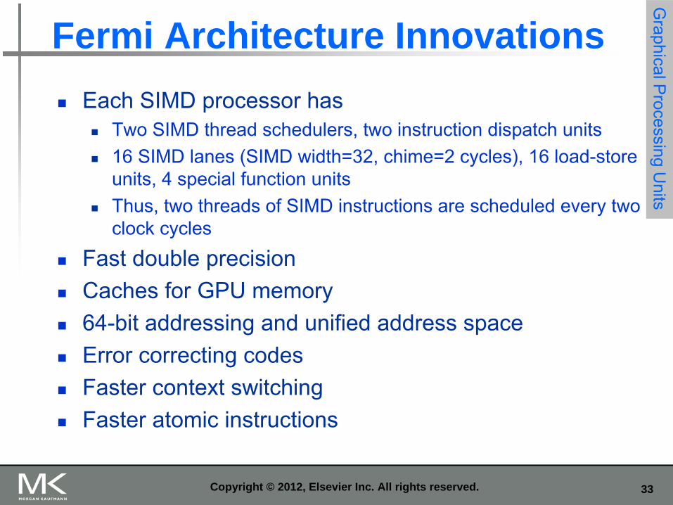
Fermi Architecture Innovations
Each SIMD processor has
Two SIMD thread schedulers, two instruction dispatch units
16 SIMD lanes (SIMD width=32, chime=2 cycles), 16 load-store units, 4 special function units
Thus, two threads of SIMD instructions are scheduled every two clock cycles
Fast double precision
Caches for GPU memory
64-bit addressing and unified address space
Error correcting codes
Faster context switching
Faster atomic instructions
Graphical P
rocessing Units

34Copyright © 2012, Elsevier Inc. All rights reserved.
Fermi Multithreaded SIMD Proc.G
raphical Processing U
nits

35Copyright © 2012, Elsevier Inc. All rights reserved.
Loop-Level Parallelism
Focuses on determining whether data accesses in later iterations are dependent on data values produced in earlier iterations
Loop-carried dependence
Example 1:for (i=999; i>=0; i=i-1)
x[i] = x[i] + s;
No loop-carried dependence
Detecting and E
nhancing Loop-Level Parallelism

36Copyright © 2012, Elsevier Inc. All rights reserved.
Loop-Level Parallelism
Example 2:for (i=0; i<100; i=i+1) {
A[i+1] = A[i] + C[i]; /* S1 */B[i+1] = B[i] + A[i+1]; /* S2 */
}
S1 and S2 use values computed by S1 in previous iteration
S2 uses value computed by S1 in same iteration
Detecting and E
nhancing Loop-Level Parallelism

37Copyright © 2012, Elsevier Inc. All rights reserved.
Loop-Level Parallelism
Example 3:for (i=0; i<100; i=i+1) {
A[i] = A[i] + B[i]; /* S1 */B[i+1] = C[i] + D[i]; /* S2 */
}
S1 uses value computed by S2 in previous iteration but dependence is not circular so loop is parallel
Transform to:A[0] = A[0] + B[0];for (i=0; i<99; i=i+1) {
B[i+1] = C[i] + D[i];A[i+1] = A[i+1] + B[i+1];
}B[100] = C[99] + D[99];
Detecting and E
nhancing Loop-Level Parallelism

38Copyright © 2012, Elsevier Inc. All rights reserved.
Loop-Level Parallelism
Example 4:for (i=0;i<100;i=i+1) {
A[i] = B[i] + C[i];D[i] = A[i] * E[i];
}
Example 5:for (i=1;i<100;i=i+1) {
Y[i] = Y[i-1] + Y[i];}
Detecting and E
nhancing Loop-Level Parallelism

39Copyright © 2012, Elsevier Inc. All rights reserved.
Finding dependencies
Assume indices are affine:
a x i + b (i is loop index)
Assume:
Store to a x i + b, then
Load from c x i + d
i runs from m to n
Dependence exists if:
Given j, k such that m ≤
j ≤
n, m ≤
k ≤
n
Store to a x j + b, load from a x k + d, and a x j + b = c x k + d
Detecting and E
nhancing Loop-Level Parallelism

40Copyright © 2012, Elsevier Inc. All rights reserved.
Finding dependencies
Generally cannot determine at compile time
Test for absence of a dependence:
GCD test:
If a dependency exists, GCD(c,a) must evenly divide (d-b)
Example:for (i=0; i<100; i=i+1) {
X[2*i+3] = X[2*i] * 5.0;}
Detecting and E
nhancing Loop-Level Parallelism

41Copyright © 2012, Elsevier Inc. All rights reserved.
Finding dependencies
Example 2:for (i=0; i<100; i=i+1) {
Y[i] = X[i] / c; /* S1 */X[i] = X[i] + c; /* S2 */Z[i] = Y[i] + c; /* S3 */Y[i] = c -
Y[i]; /* S4 */
}
Watch for antidependencies and output dependencies
Detecting and E
nhancing Loop-Level Parallelism

42Copyright © 2012, Elsevier Inc. All rights reserved.
Finding dependencies
Example 2:for (i=0; i<100; i=i+1) {
Y[i] = X[i] / c; /* S1 */X[i] = X[i] + c; /* S2 */Z[i] = Y[i] + c; /* S3 */Y[i] = c -
Y[i]; /* S4 */
}
Watch for antidependencies and output dependencies
Detecting and E
nhancing Loop-Level Parallelism

43Copyright © 2012, Elsevier Inc. All rights reserved.
Reductions
Reduction Operation:for (i=9999; i>=0; i=i-1)
sum = sum + x[i] * y[i];
Transform to…for (i=9999; i>=0; i=i-1)
sum [i] = x[i] * y[i];for (i=9999; i>=0; i=i-1)
finalsum = finalsum + sum[i];
Do on p processors:for (i=999; i>=0; i=i-1)
finalsum[p] = finalsum[p] + sum[i+1000*p];
Note: assumes associativity!
Detecting and E
nhancing Loop-Level Parallelism


