Conductance signatures of electron confinementinduced by strained nanobubbles in graphene
Dario A. Bahamon,*a Zenan Qi,b Harold S. Park,b Vitor M. Pereirac,d andDavid K. Campbelle
We investigate the impact of strained nanobubbles on the conductance characteristics of graphene nano-
ribbons using a combined molecular dynamics – tight-binding simulation scheme. We describe in detail
how the conductance, density of states, and current density of zigzag or armchair graphene nanoribbons
are modified by the presence of a nanobubble. In particular, we establish that low-energy electrons can
be confined in the vicinity of or within the nanobubbles by the delicate interplay among the pseudo-
magnetic field pattern created by the shape of the bubble, mode mixing, and substrate interaction. The
coupling between confined evanescent states and propagating modes can be enhanced under different
clamping conditions, which translates into Fano resonances in the conductance traces.
The fine control over nanofabrication techniques has not onlyincreased the performance of existing electronic devices,1 buthas also allowed the emergence of concept devices based onthe strictly quantum-mechanical properties of electrons. Onesuch proposal is the incorporation of patterned ferromagneticor superconducting films on two dimensional electron gas(2DEG) structures. Under the right conditions and design para-meters, these can be tailored to provide non-homogeneousmagnetic fields able to interact strongly with the underlyingelectrons in the ballistic transport regime.2–5 Ideally, thespatial profile of such fields should be extremely sharp alongthe transport direction and homogeneous in the transversedirection, so that the resulting magnetic barrier might behaveas an effective momentum filter, which is necessary to achievecontrol of the ballistic transmission.4,5 In addition, strong andsharp barriers generally beget richer transmission character-istics, including the stabilization of confined states within thebarrier.6 The same concept has been proposed following theadvent of graphene as a versatile two-dimensional platform fornanoscale electronic devices, with local magnetic barriersbeing one of several proposed means to confine, guide, andcontrol electron flow.7–11 The need for robust and tunable
confinement strategies is more fundamental in graphene elec-tronic devices than in conventional semiconductors becausethe massless Dirac character of the charge carriers in graphenerenders them more vulnerable to the phenomenon of Kleintunneling, and they cannot be adequately confined by stan-dard electrostatic means, particularly in the ballistic regime.However, although the search towards achieving control of theelectron flow in graphene remains one of the most activeresearch areas when it comes to applications of graphene inthe electronics industry, little progress has been made towardsthis concept of magnetic confinement. This is partly becauseof the size requirements that call for magnetic barriers that aremuch smaller than the electronic mean free path and alsobecause of the need to limit the spatial extent of the magneticfield within regions equally small, since it might be desirableto have portions of the system free of any magnetic fields. Gra-phene, with its outstanding electronic and mechanical pro-perties, offers a completely new approach towards this goal oflocal magnetic barriers that can, in principle, be modulated onscales of a few angstroms. Owing to the peculiar coupling ofelectrons and lattice deformations, it is possible to perturb thegraphene electrons in largely the same way they would react toan external magnetic field in the bulk by purely mechanicalmeans (i.e., strain).12,13 Several authors have envisaged thestudy of phenomena and applications predicted to happen inthe presence of magnetic fields by purely mechanical means,exploring appropriately engineered strain configurations toachieve desired pseudomagnetic field (PMF) profiles.14–16 Thedevelopment of Landau quantization in the absence of mag-netic fields is one such prediction17 that was recently con-firmed in local tunneling spectroscopy experiments.18,19 Thisshows that, even though strain doesn’t break time-reversal
aMackGraphe – Graphene and Nano-Materials Research Center, Mackenzie
Presbyterian University, Rua da Consolação 896, 01302-907 São Paulo, SP, Brazil.
E-mail: [email protected] of Mechanical Engineering, Boston University, Boston, MA 02215, USAcCentre for Advanced 2D Materials & Graphene Research Centre National University
of Singapore, 6 Science Drive 2, Singapore 117546, SingaporedDepartment of Physics, National University of Singapore, 2 Science Drive 3,
Singapore 117542, SingaporeeDepartment of Physics, Boston University, 590 Commonwealth Ave, Boston,
symmetry, and consequently cannot generate a quantum Halleffect or chiral edge modes as a real field would, the spectralanalogy is robust and supported by experimental evidence.Time-reversal symmetry can be explicitly broken by combiningstrain and magnetic fields, which breaks the valley degeneracyand can be explored for pseudomagnetic quantum dots whosesharp resonant tunneling characteristics might provide a verysensitive strain detector.20,21 The experiments of Levy18 andLu19 with graphene nanobubbles confirm the potential ofstrain-engineering for effective manipulation of the electronicmotion in graphene and demonstrate the unique character-istics of this approach: (i) the ability to generate local PMFswith magnitudes that can easily exceed several 100s of Tesla;(ii) the possibility of having these fields localized in regions ofonly a few nm, if strain can be locally concentrated; (iii) theprospect of continuously varying the strength of the local PMF,in particular being able to establish and remove it on demand;and (iv) not requiring drastic extrinsic modifications of the gra-phene layer, thus preserving most of its intrinsic superlatives,namely the high mobility and the Dirac nature of its carriers.Recently, in order to gain more insight into details of the PMFmagnitude and spatial profile associated with graphene nano-bubbles, as well as to understand the role played by typicalsubstrates, we (with several colleagues) conducted a study ofthe effects of nano-sized bubbles in graphene under differentgeometries and substrate conditions.22 In order to have a con-tinuous and tunable range of deflection, the nanobubbleswere generated by inflation under gas pressure against selectedapertures on the substrate.22 In the present article, we revisitthis problem from the point of view of electronic transport toelucidate the main signatures that circular and triangularnanobubbles, and their strong PMFs, imprint on the conduc-tance characteristics. We are particularly interested in whetherthe large and local PMF leads to scattering and/or confinementthat is significant enough to translate into modified trans-mission characteristics. This is directly relevant to scenariossuch as the one explored in a recent experiment that showsselective 3-point electronic transmission across pressurized tri-angular graphene nano-blisters.23 Existing theoretical workapproaches this problem by straining graphene according todeformation fields that are either prescribed analytically orobtained numerically, but always following from the equationsof continuum elasticity thus treating the graphene sheet as acontinuum medium.24,25 Hence, even when performing tight-binding calculations on the honeycomb lattice, the widespreadpractice has been to obtain the deformations from continuumelasticity theory. If this is justifiable for deformation profilesthat vary over characteristic distances that are large comparedto the lattice parameter, it isn’t so in the cases we are inter-ested to describe here. One notable exception is the approachbased on discrete differential geometry recently pioneered byBarraza-Lopez et al.26,27 which retains all the quantities para-meterized on the lattice.
We tackle this in the same framework developed in ref. 22,that combines molecular dynamics (MD) and tight-binding(TB) calculations. In this approach, the lattice deformation is
determined fully atomistically for the prescribed substrate andloading conditions, and the relaxed atomic positions are usedto build a TB description of the electron dynamics in thesystem. The aim is to reduce any bias in the description of theelectronic system by capturing all the atomic-scale details ofdeformation and curvature, without assumptions, since theyplay an important role at these scales of less than 50 nm.Similar to what is observed for real magnetic barriers6 or Gaus-sian bump deformations,28,29 the conductance of either zigzag(ZZ) or armchair (AC) graphene nanoribbons (GNR) developsmarked dips (anti-resonances) at the edge of each conductanceplateau. We show that this is due to scattering of propagatingmodes into evanescent states confined in the nanobubble. Thecoupling between the confined evanescent state and the propa-gating modes can be enhanced under different clamping andsubstrate conditions, leading to Fano resonances30–32 in theconductance traces. Our calculations show that these signa-tures of electronic confinement in graphene nanobubbles area robust effect, being observed irrespective of the orientationof the underlying graphene lattice, for circular and triangulargraphene nanobubbles on hexagonal boron nitride.
1. Model and methodology
To reproduce the deformation of graphene and its derivedtransport properties as accurately as possible, we implementeda combined MD-TB simulation. Molecular dynamics providesthe spatial location of the carbon atoms when graphene is sub-jected to gas pressure and a nanobulge forms through the sub-strate aperture. Once the coordinates of each atom are known,the nearest-neighbor TB parameters are calculated throughoutthe system and the TB Hamiltonian for the deformed system isbuilt. This Hamiltonian constitutes the basis for the calcu-lation of all the local spectral and transport properties. Elec-tronic transport is addressed via the lattice representation ofthe non-equilibrium Green’s function (NEGF).
It is beneficial to underline from the outset the role we attri-bute to the substrate in our modeling with regards to the elec-tronic structure and transport: all the electronic action is takento happen within the graphene sheet, which we assume not tobe chemically perturbed in a significant way by the presence ofthe substrate underneath. This amounts to assuming that theelectronic properties of graphene are completely decoupledfrom those of the substrate, the latter playing a rather passiverole from this perspective, in that it simply stabilizes the staticlattice configuration of graphene on which all the electronicaction unfolds. This is a reasonable assumption for mostcurrent experimental scenarios, where graphene is physicallytransferred and deposited on a target substrate with a randomorientation of the respective lattice directions. It also implicitlyassumes substrates without reactive/dangling bonds that couldstrongly interact with those pz orbitals that happen to be inregistry and become a significant source of disorder. The mostimportant aspect of this scenario of weak electronic couplingbetween graphene and the substrate is that we consider
electronic conduction taking place only through the graphenesystem, and its characteristics are determined solely by theelectronic states derived from the pz orbitals in the deformedand curved graphene. This is done so that the computationscan be easily extended to tens of thousands of atoms, andrelies on a tight-binding parameterization of the electronicdynamics that has been repeatedly shown to be reliable todescribe low energy processes such as those involved in theelectronic conduction. Moreover, a full ab initio considerationof the relaxation, electronic structure and quantum transportis unattainable in this context because (i) the deformationfields are highly non-uniform, (ii) graphene, substrate and gasatoms have to be all taken into account, and (iii) we wish totackle the characteristic deformation scales seen in the experi-ments quoted above, all of which entail a large number ofatoms in the minimal supercell. This justifies and motivatesthe multi-scale approach to this problem that we now describein more detail.
1.1 Molecular dynamics simulations
For an unbiased analysis of the local profile of deformations,the mechanical response of the system was simulated by MDwith the Sandia-developed open source code LAMMPS.34,35
The MD simulation system consisted of three subsystems: agraphene monolayer, a rigid substrate with a central aperture,and argon gas that was used to inflate graphene through theaperture to generate a nanobubble. An illustration of thesystem is shown in Fig. 1. The Tersoff potential was used todescribe the C–B–N interactions. The parameters were adoptedfrom ref. 36–38, the dimension of the simulation box was 20 ×20 × 8 nm3, and circular and triangular apertures were“etched” in the center of the substrate to allow the graphenemembrane to bulge downwards due to the gas pressure. Ineach simulation, the system was initially relaxed for 50 ps
before slowly raising the pressure to the desired target bydecreasing the volume of the gas chamber. Upon reaching thetarget pressure, the system was allowed to relax for 10 ps, afterwhich deformed configurations were obtained by averaging thecoordinates during equilibrium. Target pressures are deter-mined to yield a deflection of 1 nm. All simulations in thepresence of the gas were carried out at room temperature(300 K) using the Nose–Hoover thermostat.39
Since a previous study established that the magnitudes andspatial dependence of the strain-induced PMFs can be verysensitive to the clamping conditions and substrate type,22 weconsidered two scenarios to analyze how these effects impactthe transport signatures. In one case the MD simulations aredone with clamped boundary conditions, i.e., an ideal systemconsisting only of Ar gas and graphene, and where all carbonatoms outside the aperture region were strictly fixed. This is tostudy the effect of aperture geometry without considering thesubstrate and is similar to the approach used in previouswork.14,20,40 In the second scenario, we included a 1 nm thicksubstrate of h-BN and its interaction with the graphene sheetis explicitly taken into account. The Ar–BN (gas–substrate)interactions were neglected, and the substrate layer remainedstatic during the simulation. Most of the graphene layer wasunconstrained, except for a 0.5 nm region around the outeredges of the simulation box where it remained pinned.
The choice of the substrate is motivated by is the experi-mental observation that, for certain substrates such as boronnitride, graphene develops a nonuniform strain strong enoughto induce an energy gap ≃20 meV at the Dirac point,41–44 tointroduce satellite Dirac points,45,46 and to allow the obser-vation of a Hofstadter spectrum47 in the presence of a mag-netic field.48 Our goal is to assess whether any features in theconductance of the system when deformed under realistic con-ditions of contact with a substrate are robust, or dependent onthe degree of substrate–graphene interaction.
1.2. Tight-binding calculations
The scattering region used in the electronic transport calcu-lations contains the entire MD simulation cell (including theflat portions between the bubble’s perimeter and the edge ofthe cell). The cell accommodates 15 088 lattice sites, anexample of which is shown in Fig. 1. For convenience, we takethe x axis parallel to the ZZ direction. Most low energy elec-tronic properties of graphene are captured by the π bandnearest-neighbor TB Hamiltonian
H ¼Xki;jl
tij c†i cj þ c†j ci� �
; ð1Þ
where ci represents the annihilation operator on site i and tij isthe hopping amplitude between nearest neighbor π orbitals (inthe unstrained lattice tij = t0 ≈ −2.7 eV). The link between theMD simulation and the TB Hamiltonian is made when thepositions of the carbon atoms in the deformed configuration,obtained by MD, are incorporated into the TB Hamiltonianthrough the modification of the hopping parameter tij between
Fig. 1 Illustration of a MD simulation cell conveying the strategy usedto generate the graphene nanobubbles. An aperture (a triangle in thiscase) is perforated on hexagonal boron nitride on which rests a mono-layer of graphene (gray). Argon gas is then pressurized against graphenewhich bulges through the aperture, with a deflection that is controlledby the gas pressure. For ease of visualization the gas molecules are notshown in the picture above. Visualization is performed using VMD.33
all nearest-neighbors. The modification that accounts simul-taneously for the changing distance d between neighbors andthe local rotation of the pz orbitals is given by:
where n̂i is the unit normal to the surface at site i,~dij is the dis-tance vector connecting two sites i and j, and Vppσ(d ) andVppπ(d ) are the Slater–Koster bond integrals for σ and π bonds.Their dependence on the inter-atom distance is taken as22,49
VppπðdijÞ ¼ te�βðdij=a�1Þ; ð3Þ
VppσðdijÞ ¼ 1:7 VppπðdijÞ; ð4Þ
where t = 2.7 eV, a ≃ 1.42 Å represents the equilibrium bondlength in graphene, and β = 3.37 captures the exponentialdecrease in the hopping with interatomic distance. Once thevalues of tij are obtained, we use the TB Hamiltonian of thestrained system as the scattering central region, to which twoideal contacts are attached. This approach captures all thepossible modifications of the π-derived bands at the level ofthe Slater–Koster approximation. In particular, since nothingis assumed with regards to the position of the carbon atoms,it naturally includes effects such as the so-called pseudo-magnetic field induced by non-uniform deformations, the scalarlocal deformation potential, and sublattice symmetry breakingterms if the atomistic configurations so allow.12,13,26,28,50 Sincethe edges of the central system are of ZZ or AC type, the centralregion is seamlessly stitched to the contacts resulting in aperfect ZZ or AC ribbon. We then study the quantum transportcharacteristics of such a GNR containing a central regiondeformed by the presence of the nano-bubble. The zigzag gra-phene nanoribbon (ZGNR) is created attaching two pristinesemi-infinite ZZ nanoribbons to the left and right edges of thestrained graphene square. The metallic armchair graphenenanoribbon (AGNR) is constructed by connecting two perfectmetallic semi-infinite AGNR to the upper and lower edges ofthe central region. The conductance of these nanoribbons iscalculated within the Landauer–Büttiker formalism using
Caroli’s formula:51–53 G ¼ 2e2
hTr ΓqGrΓpGa� �
, where Gr = [Ga]† =
[E + iη − H − Σp − Σq]−1 is the retarded [advanced] Green’s
function, the coupling between the contacts and the centralregion is represented by Γq = i[Σq − Σ†
q], and Σq is the self-energy of contact q which is calculated recursively for ZZ andAC contacts.54 Having calculated the retarded and advancedGreen’s functions, other electronic properties such as the
density of states (LDOS), ρii ¼ �Im Gr ri!; ri
!;E� �� �
=π, and thetotal density of states (DOS), ρ = Tr(ρii) are readily calculated.For a local mapping of the current distribution in the centralregion we consider the current density between nearest neigh-
bors,51 Iij ¼ 2eh
ðdE tjiG,
ij � tijG,ji
h i, that is calculated from the
lesser Green’s function, and which can be obtained exactly in
the absence of electronic interactions as53 G< = Gr(E)[ΓL(E) fL(E) +ΓR(E) fR(E)]G
a(E). We stress again that the interaction graphene–substrate is included in the MD simulation part to realisticallydescribe the interaction and sliding of graphene in contactwith the substrate by the combined action of gas pressure andsubstrate aperture.55 From the electronic point of view, thesubstrate plays no direct role in electronic tunneling or otherelectronic processes.
In order to compare the local current distribution to thespatial pattern of the PMF the latter is calculated directly fromtij introduced in eqn (2) via
AxðrÞ � iAyðrÞ ¼ 2ℏ3tae
Xn
δtr;rþneiK�n: ð5Þ
This defines the two-dimensional pseudomagnetic vectorpotential, A = (Ax, Ay),
12,13 from where the PMF is calculatedusing B = ∂xAy − ∂yAx. Note that eqn (5) is used here only as apractical and direct means of quantifying the effect of the non-uniform strain in the electronic properties of graphene. It doesnot imply that we use this as an approximation for the PMF ingraphene for, as stressed above, the general and realistichopping model eqn (2) that we use in the transport calcu-lations naturally includes effects that are not captured by suchan approximation.
2. Pseudomagnetic fields,mode mixing and confinement
In order to recognize the incremental contributions of thedifferent factors determining the conductance characteristicsof the system (geometry, substrate interaction, and edge typeof the GNR), we start with the simplest scenario describedabove: a ZGNR where all carbon atoms outside the apertureare rigidly (thus artificially) attached to their original position;any deformation occurs only within the aperture region underthe gas pressure. Under this scheme the nanobubble in themiddle of the ZGNR is the only extended scattering center,which allows us to isolate the effect of the bubble geometryand the corresponding PMF on the conductance. We chosetwo representative cases of aperture geometry for discussion:triangular and circular. The triangular aperture is particularbecause it begets a PMF that is appreciably uniform withinmost of the bubble area, and which does not alternate in signwithin. The circular hole, on the other hand, is used because itcaptures most of the qualitative features of the PMF that setsin for a class of different shapes22 For a meaningful compari-son, circular and triangular bubbles are chosen with approxi-mately the same area ≃50 nm2, and centered within the squaresimulation cell; specifically, the radius of the circular apertureis 4 nm and the side length of the triangle is 10.6 nm. In asecond stage, we analyze the conductance traces arising fromthe nanobubbles inflated against a h-BN substrate to deter-mine whether the graphene–substrate interaction perturbs theconductance traces of the ideal clamped situation.
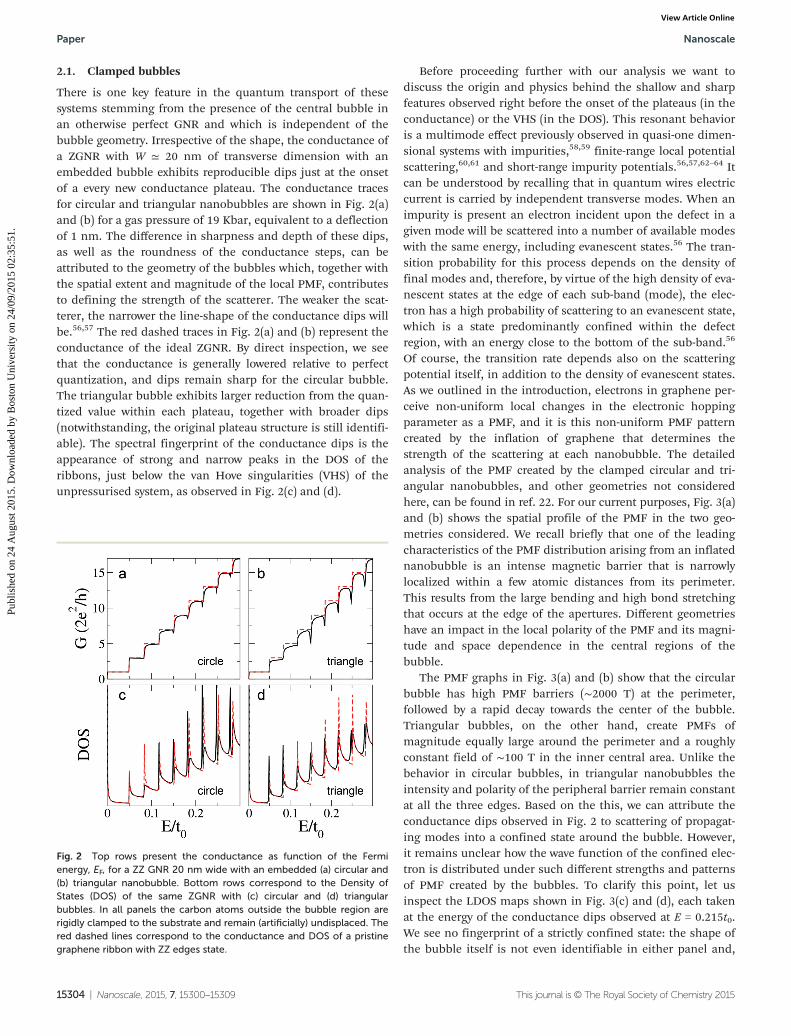
There is one key feature in the quantum transport of thesesystems stemming from the presence of the central bubble inan otherwise perfect GNR and which is independent of thebubble geometry. Irrespective of the shape, the conductance ofa ZGNR with W ≃ 20 nm of transverse dimension with anembedded bubble exhibits reproducible dips just at the onsetof a every new conductance plateau. The conductance tracesfor circular and triangular nanobubbles are shown in Fig. 2(a)and (b) for a gas pressure of 19 Kbar, equivalent to a deflectionof 1 nm. The difference in sharpness and depth of these dips,as well as the roundness of the conductance steps, can beattributed to the geometry of the bubbles which, together withthe spatial extent and magnitude of the local PMF, contributesto defining the strength of the scatterer. The weaker the scat-terer, the narrower the line-shape of the conductance dips willbe.56,57 The red dashed traces in Fig. 2(a) and (b) represent theconductance of the ideal ZGNR. By direct inspection, we seethat the conductance is generally lowered relative to perfectquantization, and dips remain sharp for the circular bubble.The triangular bubble exhibits larger reduction from the quan-tized value within each plateau, together with broader dips(notwithstanding, the original plateau structure is still identifi-able). The spectral fingerprint of the conductance dips is theappearance of strong and narrow peaks in the DOS of theribbons, just below the van Hove singularities (VHS) of theunpressurised system, as observed in Fig. 2(c) and (d).
Before proceeding further with our analysis we want todiscuss the origin and physics behind the shallow and sharpfeatures observed right before the onset of the plateaus (in theconductance) or the VHS (in the DOS). This resonant behavioris a multimode effect previously observed in quasi-one dimen-sional systems with impurities,58,59 finite-range local potentialscattering,60,61 and short-range impurity potentials.56,57,62–64 Itcan be understood by recalling that in quantum wires electriccurrent is carried by independent transverse modes. When animpurity is present an electron incident upon the defect in agiven mode will be scattered into a number of available modeswith the same energy, including evanescent states.56 The tran-sition probability for this process depends on the density offinal modes and, therefore, by virtue of the high density of eva-nescent states at the edge of each sub-band (mode), the elec-tron has a high probability of scattering to an evanescent state,which is a state predominantly confined within the defectregion, with an energy close to the bottom of the sub-band.56
Of course, the transition rate depends also on the scatteringpotential itself, in addition to the density of evanescent states.As we outlined in the introduction, electrons in graphene per-ceive non-uniform local changes in the electronic hoppingparameter as a PMF, and it is this non-uniform PMF patterncreated by the inflation of graphene that determines thestrength of the scattering at each nanobubble. The detailedanalysis of the PMF created by the clamped circular and tri-angular nanobubbles, and other geometries not consideredhere, can be found in ref. 22. For our current purposes, Fig. 3(a)and (b) shows the spatial profile of the PMF in the two geo-metries considered. We recall briefly that one of the leadingcharacteristics of the PMF distribution arising from an inflatednanobubble is an intense magnetic barrier that is narrowlylocalized within a few atomic distances from its perimeter.This results from the large bending and high bond stretchingthat occurs at the edge of the apertures. Different geometrieshave an impact in the local polarity of the PMF and its magni-tude and space dependence in the central regions of thebubble.
The PMF graphs in Fig. 3(a) and (b) show that the circularbubble has high PMF barriers (∼2000 T) at the perimeter,followed by a rapid decay towards the center of the bubble.Triangular bubbles, on the other hand, create PMFs ofmagnitude equally large around the perimeter and a roughlyconstant field of ∼100 T in the inner central area. Unlike thebehavior in circular bubbles, in triangular nanobubbles theintensity and polarity of the peripheral barrier remain constantat all the three edges. Based on the this, we can attribute theconductance dips observed in Fig. 2 to scattering of propagat-ing modes into a confined state around the bubble. However,it remains unclear how the wave function of the confined elec-tron is distributed under such different strengths and patternsof PMF created by the bubbles. To clarify this point, let usinspect the LDOS maps shown in Fig. 3(c) and (d), each takenat the energy of the conductance dips observed at E = 0.215t0.We see no fingerprint of a strictly confined state: the shape ofthe bubble itself is not even identifiable in either panel and,
Fig. 2 Top rows present the conductance as function of the Fermienergy, EF, for a ZZ GNR 20 nm wide with an embedded (a) circular and(b) triangular nanobubble. Bottom rows correspond to the Density ofStates (DOS) of the same ZGNR with (c) circular and (d) triangularbubbles. In all panels the carbon atoms outside the bubble region arerigidly clamped to the substrate and remain (artificially) undisplaced. Thered dashed lines correspond to the conductance and DOS of a pristinegraphene ribbon with ZZ edges state.
although the highest values of the LDOS are found within thebubble region, they are not significantly different from thoseoutside.
To interpret these maps it is important to note that theunpressurized conductance of these systems at E = 0.215t0 isG(0.216t0) = (2e2/h) × 11. From the conductance quantizationsequence of an ideal GNR, G = (2e2/h)(2n + 1),65,66 we concludethat there are 5 conducting modes in an ideal GNR at theenergy represented in Fig. 3(c) and (d). The inclusion of thebubbles brings only a small change to this tally, as Fig. 2shows that the conductance in their presence is, for the mostpart, scarcely modified: at E = 0.215t0 one or more channelsare backscattered because G = (2e2/h) × (10.1) for the circle,and G = (2e2/h) × (9.4) for the triangle. Despite this nominalsuppression by 1 to 2 of the conducting modes, the conduc-tance is never zero.
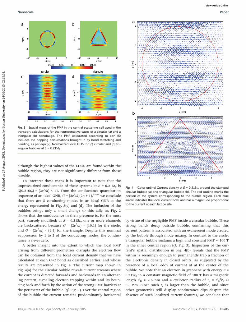
A better insight into the extent to which the local PMFarising from different geometries disrupts the electron flowcan be obtained from the local current density that we havecalculated at each C–C bond as described earlier, and whoseresults are presented in Fig. 4. The current map shown inFig. 4(a) for the circular bubble reveals current streams wherethe current is directed forwards and backwards in an alternat-ing pattern, signaling electron trapping within and its boun-cing back and forth by the action of the strong PMF barriers atthe perimeter of the bubble (cf. Fig. 3). Over the central regionof the bubble the current remains predominantly horizontal
by virtue of the negligible PMF inside a circular bubble. Thesestrong bands decay outside bubble, confirming that thiscurrent pattern is associated with an evanescent mode createdby the bubble through mode mixing. In contrast to the circle,a triangular bubble sustains a high and constant PMF ∼ 100 Tin the inner central region (cf. Fig. 3). Inspection of the cur-rent’s spatial distribution in Fig. 4(b) reveals that the PMFwithin is seemingly enough to permanently trap a fraction ofthe electronic density in closed orbits, as suggested by thepresence of a local eddy of current of at the center of thebubble. We note that an electron in graphene with energy E =0.215t0 in a constant magnetic field of 100 T has a magneticlength ℓB ≈ 2.6 nm and a cyclotron radius of rc = ℓB
2kF ≈6.8 nm. Since such rc is larger than the bubble, and sinceother geometries still display conductance dips despite theabsence of such localized current features, we conclude that
Fig. 4 (Color online) Current density at E = 0.215t0 around the clampedcircular bubble (a) and triangular bubble (b). The red outline marks theportion of the system corresponding to the bubble region. Each bluearrow indicates the local current flow, and has a magnitude proportionalto the current at each lattice site.
Fig. 3 Spatial maps of the PMF in the central scattering cell used in thetransport calculations for the representative cases of a circular (a) and atriangular (b) nanobulge. The PMF calculated according to eqn (5)includes the hopping perturbations brought in by bond stretching andbending, as per eqn (2). Normalized local DOS for (c) circular and (d) tri-angular bubbles at E = 0.215t0.
those effects are not dominated solely by the PMF but thatbubble geometry and mode mixing are important ingredients.Finally, note that an electron should have an energy higherthan E ≈ ħvFπ/L to be sensitive to a scatterer of typical size L.The average radius of the substrate apertures that we con-sidered is L ≈ 4 nm, which means that only above energies ofE ≈ 0.16t0 should the electrons begin to be noticeably affectedby the presence of the nanobubble. This estimate is quantitat-ively consistent with the fact that the conductance dips andDOS peaks, observed in Fig. 2, develop only above this energyand are not present at lower energies.
2.2. Nanobubbles on hexagonal boron nitride substrate
Whereas the previous section discusses transport in the pres-ence of a nanobubble, but with the graphene layer rigidlyclamped everywhere except the aperture region, in a realisticscenario, we must account for the graphene–substrate inter-action. The pressure-induced bulging of the graphene sheetthrough the aperture will be accompanied by its sliding andstretching in the regions outside the hole. The final strain dis-tribution will thus be different which, in turn, will lead tomodifications of the PMF barriers. Since the modification ofelectronic conductance discussed above stems from these bar-riers, one should naturally assess how robust they are in a rea-listic substrate scenario. To answer this question, we explicitlyincorporate the graphene–substrate interaction at the atomisticlevel by carrying out MD simulations of triangular and circulargraphene nanobubbles on a h-BN substrate, letting all theatoms in graphene to relax under the constraint imposed bythe gas pressure. The PMF that obtains in this case is verysimilar to that shown previously in Fig. 3(a) and (b). This is, ofcourse, not surprising given that outside the aperture regiongraphene is still being pressed against the rigid BN substrate;the magnitudes of the fields are, however, smaller, which is adirect consequence of the in-plane relaxation of the carbonatoms and the smaller in-plane strain that, consequently, setsin for the same deflection imposed on the bubble.
The implications of the modified PMF pattern to the con-ductance can be analyzed in two different energy ranges,according to whether the electron’s Fermi wavelength, λF =k/2π, is larger (E < 0.150t0) or smaller (E > 0.150t0) than thecharacteristic size of the central nanobubble. In Fig. 5(c) and(d) we show the conductance of a ZGNR with embedded circu-lar and triangular bubbles on h-BN; we can see that the con-ductance traces – specially at low energies – are now richerthan before. Interestingly, there is no marked differencebetween the two geometries; at higher energies, the presenceof the bubble translates only into shallower and wider conduc-tance dips.
One new feature detected in Fig. 5(c) and (d) is the presenceof a resonant peak right at the start of the second plateau atE ≃ 0.05t0, and which replaces the conductance plateau of theunstrained system. The dips and resonances in the conduc-tance are just two particular manifestations of a Fano reso-nance in the electron’s scattering cross-section30–32 that are
imprinted in the conductance. In simple terms, a Fano reso-nance is characterized by a transmission probability of the form
TðEÞ / ðεþ qÞ2ε2 þ 1
; ε ¼ E � Eres ð6Þ
in the neighborhood of E = Eres, where ε is the reduced energyand q the phenomenological Fano asymmetry parametermeasuring the degree of coupling between a localized (evanes-cent) state and propagating states.31,67 Whereas in general theline shape described by eqn (6) has a characteristic asymmetricprofile, if the coupling is strong (|q| → ∞) the shape reducesto a resonant symmetric peak (Breit–Wigner), while in weakcoupling (|q| → 0) it becomes a dip, or anti-resonance.
To elucidate the origin of the low-energy resonance it isinstructive to inspect the LDOS at that energy, which is shownin left panels of Fig. 6. The LDOS in the presence of the circu-lar bubble on h-BN is strongly peaked in the regions betweenthe top and bottom edges of the aperture and the outer edgesof the ribbon. Such an enhancement of the LDOS at the edgesconstitutes a fingerprint of coupling between states.68 For thisenergy E ≃ 0.05t0 at the threshold of the 1st to 2nd conduc-tance plateau, the current is carried by a single mode (one cannotice that G = G0 throughout the 1st plateau) which isstrongly localized around the edges of the nanoribbonsbecause it is one of the characteristic edge states of a ZGNR.The LDOS profile in Fig. 6(a) shows the tendency to localize
Fig. 5 (Color online) The top row shows the PMF spatial distribution for(a) circular and (b) triangular bubbles on h-BN substrate. Bottom rowsshow the conductance as a function of EF for ZZ nanoribbons 20 nmwide placed on h-BN substrate, and containing a: (a) circular nanobubbleand (b) triangular nanobubble. The red lines represent the conductanceof the same geometry bubble in the clamped configuration.
electrons between the perimeter of the circular bubble and theribbon edges, which means that the entire current pathcoming from the ZZ edge mode overlaps spatially with thelocalized state, leading to a strong-coupling scenario betweenthe confined and propagating modes. This, of course, is a con-sequence of the underlying PMF for this case: the considerable“leakage” of the PMF between the aperture and the outer edgedrives electron confinement in that region of strong field andpromotes the localization of electrons in a region throughwhich all the current would be passing, thus promoting astrong coupling that leads to a well-defined resonance. A com-parison between panels a and c at the same energy for the tri-angular bubble shows, for the latter, an asymmetricenhancement of the LDOS in the vicinity of the upper andlower edges of the ribbon. As a result, the coupling to the pro-pagating mode will not be as strong, which explains the factthat the resonance at E ≃ 0.05t0 in Fig. 5(d) is not as sharp asit is for the circular bubble. In contrast to the conductance reso-nances, the LDOS snapshots associated with dips are charac-terized by a strong enhancement in the central area, as can beseen in panels b and d of Fig. 6 for the conductance dip at E =0.116t0. For completeness, we show in Fig. 7 the respectivecurrent densities at the E = 0.116t0 dip, which support the pre-vious interpretation but show that the tendency for currentlocalization is diminished in comparison with the rigidlyclamped scenario, a consequence of the reduced strain in thepresent case.
Finally, we note that the type of graphene lead consideredin computing the conductance has no bearing on the validityof the discussion and conclusions above. To illustrate this, weshow in Fig. 8 the conductance of the same nanobubblesobtained with AC graphene nanoribbons as leads. This wasdone by connecting metallic AC leads to the vertical sides ofthe square system cell. The resulting conductance profiles areentirely similar to those seen in the ZZ transmission configur-ation, and the differences observed in the triangular case aredue to the different orientation of the triangle (a 90° rotation)with respect to the incoming current.
3. Conclusions
Using a combined molecular dynamics – tight-binding simu-lation scheme we have investigated the electronic transportproperties of graphene nanostructures containing circular andtriangular nanobubbles and under two graphene–substrate
Fig. 6 (Color online) The top row shows the normalized local DOS for acircular bubble in graphene lying on a h-BN substrate for (a) conduc-tance peak at E = 0.05t0 and (b) conductance dip at E = 0.116t0. Thebottom row refers to a triangular bubble on h-BN substrate, at (c) theconductance peak for E = 0.05t0 and (d) the conductance dip seen atE = 0.116t0.
Fig. 7 (Color online) Current density in the vicinity of the (a) circularand (b) triangular bulges when graphene lies on h-BN substrate, both atE = 0.116t0. The red outline marks the portion of the system corres-ponding to the bubble region.
adhesion conditions. The local strain that develops within andnear the bubble leads to rich patterns of strong PMF with alter-nating polarity on length scales of a few nm. The combinationof both a strong field and spatially sharp reversal of its polarityintuitively suggests a tendency for electron localization atcertain energies. We have determined how this localizationmanifests itself in (and impacts) the electronic transport. Ana-lyses of the LDOS and local current distribution reveal themicroscopic details of this localization process and establishthat low-energy electrons can be confined in the vicinity of orwithin the nanobubbles by the interplay of the specific PMFbarrier created by the geometry of the bubble, mode mixing,and substrate interaction. Interestingly, graphene substrateinteraction – unavoidable in real samples – facilitates theappearance of confined states at the same time that it deter-mines their coupling to the propagating ones. At low energies,the coupling of the evanescent electron states in the vicinity ofthe nanobubbles leads to two distinct signatures in the con-ductance as a function of EF: (i) the appearance of peaks, orBreit–Wigner resonances, when the evanescent states spreadconsiderably to the outside of the nanobubble; and (ii) dips, oranti-resonances, when these states are confined mostly insidethe nanobubble by the back and forth scattering of electronsbetween the PMF and, consequently, couple less effectively tothe continuum. We conclude that, even though under realisticconditions the interaction between graphene and the substrateis seen to modify the magnitude and spatial profile of the PMFin relation to an ideal (clamped) scenario,22 there remains asignificant tendency for electron confinement under therearranged local strain.
Acknowledgements
VMP acknowledges support through Singapore NRF CRP grant“Novel 2D materials with tailored properties: beyond gra-
phene” (R-144-000-295-281). ZQ acknowledges the support ofthe Mechanical Engineering and Physics Departments atBoston University.
References
1 R. Cavin, P. Lugli and V. Zhirnov, Proc. IEEE, 2012, 100,1720–1749.
2 A. Nogaret, J. Phys.: Condens. Matter, 2010, 22, 253201.3 S. Bending, K. von Klitzing and K. Ploog, Phys. Rev. Lett.,
1990, 65, 1060–1063.4 A. Matulis, F. Peeters and P. Vasilopoulos, Phys. Rev. Lett.,
1994, 72, 1518–1521.5 F. Peeters and A. Matulis, Phys. Rev. B: Condens. Matter,
1993, 48, 15166–15174.6 H. Xu, T. Heinzel, M. Evaldsson, S. Ihnatsenka and
I. Zozoulenko, Phys. Rev. B: Condens. Matter, 2007, 75,205301.
7 A. De Martino, L. Dell’Anna and R. Egger, Phys. Rev. Lett.,2007, 98, 066802.
8 M. Ramezani Masir, P. Vasilopoulos, A. Matulis andF. Peeters, Phys. Rev. B: Condens. Matter, 2008, 77, 235443.
9 M. R. Masir, P. Vasilopoulos and F. M. Peeters, J. Phys.:Condens. Matter, 2011, 23, 315301.
10 L. Oroszlány, P. Rakyta, A. Kormányos, C. Lambert andJ. Cserti, Phys. Rev. B: Condens. Matter, 2008, 77, 081403.
11 A. Kormányos, P. Rakyta, L. Oroszlány and J. Cserti, Phys.Rev. B: Condens. Matter, 2008, 78, 045430.
12 C. L. Kane and E. J. Mele, Phys. Rev. Lett., 1997, 78,1932.
13 H. Suzuura and T. Ando, Phys. Rev. B: Condens. Matter,2002, 65, 235412.
14 F. Guinea, B. Horovitz and P. Le Doussal, Phys. Rev. B:Condens. Matter, 2008, 77, 205421.
15 V. M. Pereira and A. H. Castro Neto, Phys. Rev. Lett., 2009,103, 4.
16 M. A. H. Vozmediano, M. I. Katsnelson and F. Guinea,Phys. Rep., 2010, 496, 109–148.
17 F. Guinea, M. I. Katsnelson and A. K. Geim, Nat. Phys.,2010, 6, 30–33.
18 N. Levy, S. A. Burke, K. L. Meaker, M. Panlasigui, A. Zettl,F. Guinea, A. H. C. Neto and M. F. Crommie, Science, 2010,329, 544–547.
19 J. Lu, A. H. Castro Neto and K. P. Loh, Nat. Commun., 2012,3, 823.
20 K.-J. Kim, Y. M. Blanter and K.-H. Ahn, Phys. Rev. B:Condens. Matter, 2011, 84, 081401.
21 Z. Qi, D. A. Bahamon, V. M. Pereira, H. S. Park,D. K. Campbell and A. H. Castro Neto, Nano Lett., 2013, 13,2692–2697.
22 Z. Qi, A. L. Kitt, H. S. Park, V. M. Pereira, D. K. Campbelland A. H. Castro Neto, Phys. Rev. B: Condens. Matter, 2014,90, 125419.
23 J. Aguilera-Servin, T. Miao and M. Bockrath, Appl. Phys.Lett., 2015, 106, 083103.
Fig. 8 (Color online) Conductance of a 20 nm AC nanoribbon with atriangular bubble in the central region. The different curves correspondto the conductance of a pristine ribbon (red), a bubble under clampedconditions (blue), and a bubble on the h-BN (black) substrate.
24 D. A. Gradinar, M. Mucha-Kruczyński, H. Schomerus andV. I. Fal’ko, Phys. Rev. Lett., 2013, 110, 266801.
25 D. A. Cosma, M. Mucha-Kruczyński, H. Schomerus andV. I. Fal’ko, Phys. Rev. B: Condens. Matter, 2014, 90, 245409.
26 S. Barraza-Lopez, A. A. P. Sanjuan, Z. Wang and M. Vanević,Solid State Commun., 2013, 166, 70–75.
27 A. A. P. Sanjuan, Z. Wang, H. P. Imani, M. Vanevic andS. Barraza-Lopez, Phys. Rev. B: Condens. Matter, 2014, 89,121403(R).
28 R. Carrillo-Bastos, D. Faria, A. Latgé, F. Mireles andN. Sandler, Phys. Rev. B: Condens. Matter, 2014, 90, 041411.
29 M. Settnes, S. R. Power, J. Lin, D. H. Petersen andA.-P. Jauho, Phys. Rev. B: Condens. Matter, 2015, 91, 125408.
30 U. Fano, Phys. Rev., 1961, 124, 1866–1878.31 A. Miroshnichenko, S. Flach and Y. Kivshar, Rev. Mod.
Phys., 2010, 82, 2257–2298.32 J. Nöckel and A. Stone, Phys. Rev. B: Condens. Matter, 1994,
50, 17415–17432.33 W. Humphrey, A. Dalke and K. Schulten, J. Mol. Graphics,
1996, 14, 33–38.34 Lammps, http://lammps.sandia.gov, 2012.35 S. Plimpton, J. Comput. Phys., 1995, 117, 1–19.36 C. Sevik, A. Kinaci, J. B. Haskins and T. Çağın, Phys. Rev. B:
Condens. Matter, 2011, 84, 085409.37 C. Sevik, A. Kinaci, J. B. Haskins and T. Çağın, Phys. Rev. B:
Condens. Matter, 2012, 86, 075403.38 L. Lindsay and D. A. Broido, Phys. Rev. B: Condens. Matter,
2010, 81, 205441.39 W. G. Hoover, Phys. Rev. A, 1985, 31, 1695–1697.40 P. Wang, W. Gao, Z. Cao, K. M. Liechti and R. Huang,
J. Appl. Mech., 2013, 80, 040905.41 B. Hunt, J. D. Sanchez-Yamagishi, A. F. Young,
M. Yankowitz, B. J. LeRoy, K. Watanabe, T. Taniguchi,P. Moon, M. Koshino, P. Jarillo-Herrero and R. C. Ashoori,Science, 2013, 340, 1427–1430.
42 J. Jung, A. M. DaSilva, A. H. MacDonald and S. Adam, Nat.Commun., 2015, 6, 6308.
43 M. Neek-Amal and F. M. Peeters, Appl. Phys. Lett., 2014,104(4), 041909.
44 P. San-Jose, A. Gutiérrez-Rubio, M. Sturla and F. Guinea,Phys. Rev. B: Condens. Matter, 2014, 90, 075428.
45 L. A. Ponomarenko, R. V. Gorbachev, G. L. Yu, D. C. Elias,R. Jalil, A. A. Patel, A. Mishchenko, A. S. Mayorov,C. R. Woods, J. R. Wallbank, M. Mucha-Kruczynski,B. A. Piot, M. Potemski, I. V. Grigorieva, K. S. Novoselov,F. Guinea, V. I. Fal’ko and A. K. Geim, Nature, 2013, 497,594–597.
46 M. Yankowitz, J. Xue, D. Cormode, J. D. Sanchez-Yamagishi,K. Watanabe, T. Taniguchi, P. Jarillo-Herrero, P. Jacquod andB. J. LeRoy, Nat. Phys., 2012, 8, 382–386.
47 D. R. Hofstadter, Phys. Rev. B: Solid State, 1976, 14, 2239–2249.
48 G. L. Yu, R. V. Gorbachev, J. S. Tu, A. V. Kretinin, Y. Cao,R. Jalil, F. Withers, L. A. Ponomarenko, B. A. Piot,M. Potemski, D. C. Elias, X. Chen, K. Watanabe,T. Taniguchi, I. V. Grigorieva, K. S. Novoselov, V. I. Fal’ko,A. K. Geim and A. Mishchenko, Nat. Phys., 2014, 10, 525–529.
49 V. M. Pereira, A. H. Castro Neto and N. M. R. Peres, Phys.Rev. B: Condens. Matter, 2009, 80, 045401.
50 J. L. Mañes, F. de Juan, M. Sturla andM. A. H. Vozmediano, Phys. Rev. B: Condens. Matter, 2013,88, 155405.
51 C. Caroli, R. Combescot, P. Nozieres and D. Saint-James,J. Phys. C: Solid State Phys., 1971, 4, 916.
52 S. Datta, Electronic Transport in Mesoscopic Systems, Cam-bridge University Press, 1995.
53 H. Haug and A.-P. Jauho, Quantum Kinetics in Transport andOptics of Semiconductors, Springer, Berlin, Heidelberg,2008, vol. 123, pp. 181–212.
54 M. P. L. Sancho, J. M. L. Sancho, J. M. L. Sancho andJ. Rubio, J. Phys. F: Met. Phys., 1985, 15, 851.
55 A. L. Kitt, Z. Qi, S. Rémi, H. S. Park, A. K. Swan andB. B. Goldberg, Nano Lett., 2013, 13, 2605–2610.