NT96655 2013/07/30 - 1 - Version 0.8 With respect to the information represented in this document, Novatek makes no warranty, expressed or implied, including the warranties of merchantability, fitness for a particular purpose, non-infringement, or assumes any legal liability or responsibility for the accuracy, completeness, or usefulness of any such information. NT96655 Hybrid DSC/DV Processor Version 0.8 Preliminary CONFIDENTIAL
Transcript
NT96655
20130730 - 1 - Version 08 With respect to the information represented in this document Novatek makes no warranty expressed or implied including the warranties of merchantability fitness for a particular purpose non-infringement or assumes any legal liability or responsibility for the accuracy completeness or usefulness of any such information
NT96655 Hybrid DSCDV Processor
Version 08
Preliminary
CONFIDEN
TIAL
Administrator
打字机
深圳睿鹰科技有限公司
Administrator
打字机
Administrator
打字机
Administrator
打字机
Administrator
打字机
Administrator
打字机
Administrator
打字机
NT96655
20130730 - 2 - Version 08 With respect to the information represented in this document Novatek makes no warranty expressed or implied including the warranties of merchantability fitness for a particular purpose non-infringement or assumes any legal liability or responsibility for the accuracy completeness or usefulness of any such information
20130730 - 3 - Version 08 With respect to the information represented in this document Novatek makes no warranty expressed or implied including the warranties of merchantability fitness for a particular purpose non-infringement or assumes any legal liability or responsibility for the accuracy completeness or usefulness of any such information
51 Power on Sequence34 52 General IO37 53 Specific function IO(RTC Reset LVD and PBC) 40 54 DRAM41 55 High speed serial interface(MIPI CSI LVDS HiSPi) 43 56 ADC 45 57 Audio Codec45 58 TV encoder46 59 MIPI DSI Tx 47 510 HDMI Tx51 511 USB 52 512 USB Charging Port Detect 56
CONFIDEN
TIAL
Administrator
打字机
深圳睿鹰科技有限公司
NT96655
20130730 - 4 - Version 08 With respect to the information represented in this document Novatek makes no warranty expressed or implied including the warranties of merchantability fitness for a particular purpose non-infringement or assumes any legal liability or responsibility for the accuracy completeness or usefulness of any such information
Revision History Rev Date Author Contents 01 20120213 Kevin Hung First draft version 02 20120316 Kevin Hung For PM 03 20120907 Kevin Hung Add pin number amp DDR_PHY(DLL) power issue (ES version)
04 20120928 Kevin Hung
Change AVDD_MPLL10V 15V Exchange function pin-out about SN_SHUTTER and SN_FLASH Exchange Microphone R-ch and L-ch Remove HV description 1 Update GPIO pull updown spec 2 Change RESET HIS IOz pull updown resistor symbol 3 Add IOSS driving and pull updown DC characteristics 4 Add IOs2 driving spec 5 Change IO 25V spec to 28V spec 6 Add RESET pin Schmitt trigger level spec
05 20121129 Roy Lo
7 change TV_RADJrsquos resistor 470430 Ohm 05 20121220 Roy Lo Update DDRIII IO drivingsinking spec 05 20130118 Kevin Hung Remove DR_CS modify N4K3 pin define for Ver AB 05 20130311 Joel Update CPU amp DRAM max operating frequency 06 20130513 Kevin Hung Modify default status of MC14 internal resistor from pu pd 06 20130514 Kevin Hung Exchange N4K3 pin define for Ver BC 07 20130614 Kevin Hung Add NT96656 in this common version 08 20130730 Kevin Hung Separate from common version
CONFIDEN
TIAL
Administrator
打字机
深圳睿鹰科技有限公司
NT96655
20130730 - 5 - Version 08 With respect to the information represented in this document Novatek makes no warranty expressed or implied including the warranties of merchantability fitness for a particular purpose non-infringement or assumes any legal liability or responsibility for the accuracy completeness or usefulness of any such information
Features High Performance 32-bit CPU
MIPS32 24Kec with ASE DSP extension MMU embedded 16KB instruction and 16KB data cache Embedded ICE makes firmware debugging easier CPU operating frequency up to 432MHz on the fly programmable
Power Management Features Firmware configurable operating frequency of each functional block to meet best power
Scalable Memory Bus Architecture 16-bit DDR2 DDR3 SDRAM bus supporting up to 2Gb DDR SDRAM DRAM operating frequency up to 373MHz without ODT Tunable DDR frequency on the fly for power saving
Sensor Interface Engine Support up to 50M pixels CCDCMOS image sensor Support high speed serial interface like sub-LVDSMipiHiSPi up to 10 channels for most
commercial CMOS sensors including Sony Panasonic Aptina Samsung Sharp and Omnivision etc (8 channels for dual MIPI version)
Support parallel sensor interface for most commercial CCD sensors including Sony Panasonic Sharp and CMOS sensors including Aptina and Omnivision
Support BT601656 video input Support dual sensors input (dual MIPI version only) Support 12-bit (serial) sensor data input Support high speed serial interface sensor pixel rate up to 576MPixelssec Support continuous shot up to 10 fps for 16MP sensor Support parallel interface sensor pixel clock up to 108MHz Support movie CCD and horizontal division CCD of SONY CONFI
DENTI
AL
Administrator
打字机
深圳睿鹰科技有限公司
NT96655
20130730 - 6 - Version 08 With respect to the information represented in this document Novatek makes no warranty expressed or implied including the warranties of merchantability fitness for a particular purpose non-infringement or assumes any legal liability or responsibility for the accuracy completeness or usefulness of any such information
Support multiple field line interleaved CCD of Sharp Support smear reduction for CCD sensor Built-in color pattern generation Sensor black level clamping Efficient defect concealment algorithm Raw image sub-sample for video amp high ISO image Flexible image analysis flow for AE AWB and AF purpose Programmable histogram analysis Automatic flicker detection RGB Gamma LUT for sensor linearization correction In-pipeline lens shading compensation technology In-pipeline color shading compensation technology In-pipeline geometric distortion correction technology In-pipeline color aberration correction technology Support CMOS sensor spatial crosstalk cancellation Support in-frame dark frame subtraction with smart defect detection algorithm Support rolling shutter correction for CMOS sensor Mechanical shutter control Flash light control
Image Processing Engine Proprietary advanced anti-alias Bayer CFA color interpolation Flexible edge rendering control and enhancement Powerful noise reduction technology for still and video recording Support motion compensated temporal filtering (MCTF) for efficient video noise reduction Support temporal noise reduction with ghost reduction RGB Gamma LUT High precision color correction matrix for sRGB or specific color requirement Brightnesscontrast and huesaturation adjustment Specific color control technology (Patent) 3D color conversion for specific color preference tuning False color suppression Support wide dynamic range (WDR) for local illumination enhancement
Image Manipulation Engine High quality scaling engine for seamless digital zooming from 116x to 16x CONFI
DENTI
AL
Administrator
打字机
睿鹰-高品质行车记录仪专家
NT96655
20130730 - 7 - Version 08 With respect to the information represented in this document Novatek makes no warranty expressed or implied including the warranties of merchantability fitness for a particular purpose non-infringement or assumes any legal liability or responsibility for the accuracy completeness or usefulness of any such information
Support thumbnail image generation Forwardinverse color space transform
Face Detection Engine Very high speed face detection and tracking High accuracy under different light source Programmable target data base
Digital Image Stabilizer Remove unintended hand movement from an image sequence Single frame compensation for video (Total compensation) Accumulate frame compensation for video (Smart compensation) Motion refresh rate 60Hz
Interface search range up to 32 Programmable total compensation range Accommodate resolution 1080p Adjustable number of motion vectors for motion estimation Maximum 1024 motion vectors
per process (16 regions x 64 blocksregion)
LCDTV Display Support dual display including LCD panel and HDMITV display simultaneously High performance scaling updown engine programmable gamma correction color
transform and color management for LCD or TV display Separate OSD for LCD panel and TV Support digital LCD interface for AUO Casio CMI (all digital panels will be supported) Support 16-bit RGB parallel interface (RGB565 or Delta RGB) LCD panel up to 1024x1024
resolution Support MIPI DSI for mobile display Support 90∘rotationflipmirror
Support PAL NTSC video encoder (CVBS format) Integrated 1 internal 10-bit video DACs Support digital interface BT6016561120 output port 33V 18V LCD Digital video out
HDMI Support HDMI v13a Support DDC with maximum 100khz access rate for CEA-861-D format Support CEC CONFI
DENTI
AL
Administrator
打字机
睿鹰-高品质行车记录仪专家
NT96655
20130730 - 8 - Version 08 With respect to the information represented in this document Novatek makes no warranty expressed or implied including the warranties of merchantability fitness for a particular purpose non-infringement or assumes any legal liability or responsibility for the accuracy completeness or usefulness of any such information
Support 16 bits PCM 32 KHz 441 KHz 48KHz for maximum 2 channels audio output
Graphic Engine Copy and paste Geometric operation including mirror flip and rotation Arithmetic operation including addition subtraction color keying logic operation and alpha
blending Support warping function Support anti-alias affine transform Support hardware acceleration for multi-frame processing
Cipher 64-bit DES 3DES and AES-128 Both encryption and decryption Big and little endian of input data
H264AVC CODEC Support encoder BPMP level 41 Support encoder HP level 42 Support real-time capability for 1080p30 720p60 480p120 Support full frame still capture while video recording H264 highmain profile 1 reference picture for P-frame 2 reference pictures for B-frame Support video format MP4 AVI MOV Support bit rate control Automatic frame sync for high frame rate
Motion Estimation [-12475+12475] search range in horizontal component [-2875 +2875] search range in vertical component MB mode 16x16 16x8 8x16 8x8 skip and direct (B-frame)
FW Audio CODEC AAC encode decode (32KHz 48KHz 192kbps) ADPCM encode decode Noise cancellation for background noise motor operation and wind
20130730 - 9 - Version 08 With respect to the information represented in this document Novatek makes no warranty expressed or implied including the warranties of merchantability fitness for a particular purpose non-infringement or assumes any legal liability or responsibility for the accuracy completeness or usefulness of any such information
JPEG CODEC Supports Motion JPEG 30fps1080P30 video clipplayback function Max pixel clock 120Mpixel sec Support ISOIEC 10918-1 baseline JPEG compressiondecompression Still image maximum resolutions will be up to 65536x65536 pixels Support input format 422 420 411 400 211 JPEG supports downloadable Quantization and Huffman tables Support Exchangeable Image File format (EXIF 223 and newer) Support MPO file format for 3D image
Digital Audio Interface Support I2S codec interface Audio clock generator
Dual Graphic-based OSD Support 8-bit palette and ARGB(4565 or 8565) OSD architecture 256 colors simultaneously out of true color at 8-bit palette OSD 8 levels of opacity for 8-bit palette OSD Programmable width amp height to meet LCDTVs resolution exactly Picture in picture function Dedicated 16 face frames for face detection function
Storage Memory Controller Secure Digital card and SDIO Support SD 30 Support UHS-I UHS50 UHS104 (Max freq 108MHz) Support eMMC and hot boot Support eyeFi for wireless connection Multi-Media card SLC NAND type flash
USB Fully compliant with USB20 devicehost High speed (480Mbps) supported CONFI
DENTI
AL
Administrator
打字机
QQ848478751
Administrator
打字机
NT96655
20130730 - 10 - Version 08 With respect to the information represented in this document Novatek makes no warranty expressed or implied including the warranties of merchantability fitness for a particular purpose non-infringement or assumes any legal liability or responsibility for the accuracy completeness or usefulness of any such information
Optionally switchable to be fully compliant with USB 11 Support Control Isochronous Interrupt and Bulk transfer Support PC camera mode
Timers RTC can be powered by separate backup battery and operating from 15V to 36V Watch dog timer 16 programmable HW timers support resolution up to 3MHz and 32 bits counter
Peripheral Interface Support I2C interface Support 20 channels PWM including built-in 16 (4 sets) pattern generators for micro-Stepping
motor control Support GPIO and flexible PWM interface with micro-stepping Support programmable 3-wired serial interface Support SPI for gyroscope reading Support UART interface Support 8 channels of 10-bit ADC with touch panel interface (2 channels) the max sample
rate up to 125 KHz per channel
On-chip Boot Strap Loader Built-in on-chip mask ROM User program can be stored in NAND-type flash and external static memory is not
necessary On-chip mask ROM can be disabled System can boot from SPI flash NAND flash memory cards eMMC and USB
Triple Voltage Power Supply 105V core logic voltage 18V 15V DDRIIDDRIII SDRAM interface voltage 33V IO interface and analog circuit voltage
Package NT96655BG 305 ball TFBGA 13x13 mm2
CONFIDEN
TIAL
Administrator
打字机
QQ848478751
Administrator
打字机
NT96655
20130730 - 11 - Version 08 With respect to the information represented in this document Novatek makes no warranty expressed or implied including the warranties of merchantability fitness for a particular purpose non-infringement or assumes any legal liability or responsibility for the accuracy completeness or usefulness of any such information
General Description NT9665xBG is a high image quality high performance power saving and cost effective digital still camera (DSC) and digital video camera (DV) controller with excellent digital still image capturing and video streaming capabilities It is targeted for the application of VGA to 50M pixel DSCDV resolutions It can be easily adapted to many high speed CMOS and conventional CCD image sensors with on chip programmable interface timing approach The controller provides sophisticated video processing methods with built-in hardware acceleration pipeline This is essential for achieving high performance for per-shot shot-to-shot and continuous shooting pictures The controller provides flexible mechanism for auto white balance auto exposure and auto-focusing in order to better tradeoff hardware and software efforts over the performance Embedded H264 video CODEC supports video recording up to full-HD 1080p30 The HDMI 13 Tx is also equipped for HDTV output Rich storage interfaces are supported to make it ideal for the storage of still pictures and video streaming data The USB20 high speed interface can uploaddownload the audiovideo data efficiently tofrom PC
CONFIDEN
TIAL
Administrator
打字机
QQ848478751
Administrator
打字机
Administrator
打字机
Administrator
打字机
NT96655
20130730 - 12 - Version 08 With respect to the information represented in this document Novatek makes no warranty expressed or implied including the warranties of merchantability fitness for a particular purpose non-infringement or assumes any legal liability or responsibility for the accuracy completeness or usefulness of any such information
Block Diagram
SENSOR PORT A
SENSOR PORT B
IMAGPROCESSOR
FHD H264CODEC
JPEGCODEC
FACE DETECTDISTORTIONCORR
SCALER
CPUMIPS32 24KEc
GRAPHICS
TVENCODER
AUDIO CODECamp I2S
HDMI 13 TX
DDR PHY
PWM
RTC WDT
I2C
NAND
SIF
SDSDIOx2
USB 20HOSTDEV UART
ADC
GPIO
MOTION ESTIMATOR
LCD
SPI
DDR DMA
BT 656BT1120
CIPHER
PLL
32768KHz
12MHzDDR23
TV
LCD PANEL
PC
WIRELESS
Wi-Fi3G4GNAND FLASH SD CARD
DRAM
LENS amp SENSOR
2nd OPTIONALSENSOR MODULE
CONFIDEN
TIAL
Administrator
打字机
QQ848478751
Administrator
打字机
Administrator
打字机
Administrator
打字机
NT96655
20130730 - 13 - Version 08 With respect to the information represented in this document Novatek makes no warranty expressed or implied including the warranties of merchantability fitness for a particular purpose non-infringement or assumes any legal liability or responsibility for the accuracy completeness or usefulness of any such information
Pin Configuration
1 TFBGA-305
CONFIDEN
TIAL
NT96655
20130730 - 14 - Version 08 With respect to the information represented in this document Novatek makes no warranty expressed or implied including the warranties of merchantability fitness for a particular purpose non-infringement or assumes any legal liability or responsibility for the accuracy completeness or usefulness of any such information
Pin No Pin Name Pin No Pin Name Pin No Pin Name Pin No Pin Name A1 DR_D9 E19 I2C_SDA K11 GND R3 DR_A0 A2 DR_D14 F1 DR_DQM0 K12 GND R17 JTAG_TRST A3 FL_TRIG F2 DR_DQM1 K13 VDDK R18 XTAL_SYSO A4 SN_DGPIO5 F3 VDD_DR K14 AVDD_HDMI R19 XTAL_SYSI A5 SN_SCK F6 SP_CLK K16 AVDD_DAC T1 DR_A5 A6 SN_VD F7 PWM6 K17 TV_FSADJ T2 DR_A3 A7 HSI_D0P F8 AVDD_HSI_K K18 HDMI_TX0P T3 DR_A6 A8 HSI_D2P F9 AVDD_HSI_RX K19 HDMI_TX0N T4 MC5 A9 HSI_D4P F10 VDD_HSI_IO L1 DR_D2 T7 MC8
20130730 - 15 - Version 08 With respect to the information represented in this document Novatek makes no warranty expressed or implied including the warranties of merchantability fitness for a particular purpose non-infringement or assumes any legal liability or responsibility for the accuracy completeness or usefulness of any such information
20130730 - 16 - Version 08 With respect to the information represented in this document Novatek makes no warranty expressed or implied including the warranties of merchantability fitness for a particular purpose non-infringement or assumes any legal liability or responsibility for the accuracy completeness or usefulness of any such information
Pin Descriptions I = input port with Schmitt trigger O = output port with normal drivingsinking IO = bi-directional port with normal drivingsinking and Schmitt input mvIO = multi voltage bi-direction port with Schmitt input HSI = high speed serial interface with multi voltage input port IOsw = bi-directional port with strong drivingsinking and wide Schmitt input range IOw = bi-directional port with wide Schmitt input range IOs = bi-directional port with strong drivingsinking IOs2 = bi-directional port with strong drivingsinking IOss = bi-directional port with strong drivingsinking IOz = bi-directional port with large pulldown resistor IO5VT = bi-directional port with normal drivingsinking and Schmitt input OD = open drain output with normal sinking IOD = bi-directional port open drain output LVD = low voltage detect function pin pu = internal pull-up pd = internal pull-down AI = analog input port AI5VT = analog 5V tolerant input port AO = analog output port AIO = analog bi-directional port H = output high L = output low P = power or ground Note means this pin has interrupted function
CONFIDEN
TIAL
NT96655
20130730 - 17 - Version 08 With respect to the information represented in this document Novatek makes no warranty expressed or implied including the warranties of merchantability fitness for a particular purpose non-infringement or assumes any legal liability or responsibility for the accuracy completeness or usefulness of any such information
1 NT96655BG 305 pins
Total 305 pins Alternative GPIO 133 pins
11 System interface (9) Pin No Name Type Reset Descriptions
R19 XTAL_SYSI AI - Crystal input for system oscillator (12MHz) R18 XTAL_SYSO AO - Output for system oscillator
B15 RESET LVD pu System Reset Connect a capacitor to ground for reset time control
J12 TESTEN I I pd Test mode enable Keep low for normal operation
R17 JTAG_TRST P_GPIO[31] IO I pu JTAG test logic reset(active low)
N14 JTAG_TMS P_GPIO[32] IO I pd JTAG test mode select
P17 JTAG_TCK P_GPIO[33] IO I pd JTAG test clock input
P18 JTAG_TDI P_GPIO[34] IO I pd JTAG test data input
P19 JTAG_TDO P_GPIO[35] IO I pd JTAG test data output
12 RTC amp Power Button Controller (7) Pin No Name Type Default Descriptions
A14 XTAL_RTCI AI - Crystal input for real time clock oscillator (32768KHz) B14 XTAL_RTCO AO - Output for real time clock oscillator C14 PWR_SW1 AI I pd Power onoff signal input (ONOFF switch use) B13 PWR_SW2 AI I pu Power onoff signal input (falling edge trigger)
H12 PWR_SW3 I5VTZ I pd Power onoff signal input (5V tolerance Input for VBUSI use)
D13 PWR_SW4 AI I pd Power onoff signal input (Bettery in use) A13 PWR_EN AO - Power enable signal output
PWR_SW can trigger interrupt (share RTC interrupt) If this pin isnrsquot used Novatek recommends connecting this pin to GND
13 DRAM interface (47) Pin No Name Type Reset Descriptions
M4 DR_RESET O - Reset signal output for DDR3 DRAM M1 DR_CLK O - M2 DR_CLK O - DRAM differential clock output
N2 DR_CKE O - DRAM clock enable CONFIDEN
TIAL
NT96655
20130730 - 18 - Version 08 With respect to the information represented in this document Novatek makes no warranty expressed or implied including the warranties of merchantability fitness for a particular purpose non-infringement or assumes any legal liability or responsibility for the accuracy completeness or usefulness of any such information
M3 DR_CAS
L3 DR_RAS N3 DR_WE
O - DRAM control signals
J4 DR_VREF AI - DRAM reference voltage input P1 DR_BA0 N1 DR_BA1 P2 DR_BA2
IO - DRAM data bus inputoutput upper byte (Each bits of upper byte may be permuted to make routing simpler)
CONFIDEN
TIAL
NT96655
20130730 - 19 - Version 08 With respect to the information represented in this document Novatek makes no warranty expressed or implied including the warranties of merchantability fitness for a particular purpose non-infringement or assumes any legal liability or responsibility for the accuracy completeness or usefulness of any such information
14 Sensor interface (33) Pin No Name Type Reset Descriptions
B7 HSI_D0N S_GPI[0]
A7 HSI_D0P S_GPI[1]
D8 HSI_D1N S_GPI[2]
C8 HSI_D1P S_GPI[3]
B8 HSI_D2N S_GPI[4]
A8 HSI_D2P S_GPI[5]
D9 HSI_D3N S_GPI[6]
C9 HSI_D3P S_GPI[7]
B9 HSI_D4N S_GPI[8]
A9 HSI_D4P S_GPI[9]
B10 HSI_CK0N S_GPI[10]
A10 HSI_CK0P S_GPI[11]
D10 HSI_D5N S_GPI[12]
C10 HSI_D5P S_GPI[13]
B11 HSI_D6N S_GPI[14]
A11 HSI_D6P S_GPI[15]
D11 HSI_D7N S_GPI[16]
C11 HSI_D7P S_GPI[17]
B12 HSI_D8N S_GPI[18]
A12 HSI_D8P S_GPI[19]
D12 HSI_D9N S_GPI[20]
C12 HSI_D9P S_GPI[21]
HSI I pd
High speed differential sensor interface and parallel interface (when sensor interface is configured as high speed differential sensor interface the clock lane should be a dedicated differential lane And each data lanes may be permuted in established group refer to below table)
CONFIDEN
TIAL
NT96655
20130730 - 20 - Version 08 With respect to the information represented in this document Novatek makes no warranty expressed or implied including the warranties of merchantability fitness for a particular purpose non-infringement or assumes any legal liability or responsibility for the accuracy completeness or usefulness of any such information
D7 SN_MCLK S_GPIO[24] mvIOs I pd Programmable Clock output for sensor
C7 SN_PXCLK S_GPIO[25] mvIOs I pd Sensor Pixel Clock Input
mvIOs I pu General serial interface 0 or Serial Peripheral Interface 3 Chip Select
A5
SN_SCK SPI3_CLK I2C_SCL P_GPIO[57]
mvIOD I pu General serial interface 0 or Serial Peripheral Interface 3 clock output I2C-BUS clock output(Open Drain IO structure)
B5
SN_DAT SPI3_DO I2C_SDA P_GPIO[58]
mvIOD I pu General serial interface 0 or Serial Peripheral Interface 3 data output I2C-BUS data input output(Open Drain IO structure)
C5 SN_DGPIO4 mvIO I pd General purpose Input output A4 SN_DGPIO5 mvIO I pd General purpose Input output
B4 SPI3_DI SN_FLASH SN_DGPIO6
mvIO I pd Serial Peripheral Interface 3 data input Flash Signal input from sensor
C4 SN_SHUTTER SN_DGPIO7 mvIO I pd Shutter signal input from sensor
Note The pin can trigger interrupt Note1 The input voltage of HSI corresponds to GVDD_SN Note2 The mvIO voltage of Sensor interface corresponds to VDD_SN
Name LVDS HiSPi MIPI CSI Parallel (12 bits) CCIR601 (16 bits) CCIR601 (8 bits) S_GPI[0] HSI_D0N I SLVS_D0N I CSI_D0N I SN_D0 I S_GPI[1] HSI_D0P I SLVS_D0P I CSI_D0P I SN_D1 I S_GPI[2] HSI_D1N I SLVS_D1N I CSI_D1N I SN_D2 I S_GPI[3] HSI_D1P I SLVS_D1P I CSI_D1P I SN_D3 I S_GPI[4] HSI_D2N I SLVS_D2N I CSI_D2N I SN_D4 I CCIR_Y0 I S_GPI[5] HSI_D2P I SLVS_D2P I CSI_D2P I SN_D5 I CCIR_Y1 I S_GPI[6] HSI_D3N I SLVS_D3N I CSI_D3N I SN_D6 I CCIR_Y2 I S_GPI[7] HSI_D3P I SLVS_D3P I CSI_D3P I SN_D7 I CCIR_Y3 I S_GPI[8] HSI_D4N I SN_D8 I CCIR_Y4 I S_GPI[9] HSI_D4P I SN_D9 I CCIR_Y5 I S_GPI[10] HSI_CK0N I SLVS_CKN I CSI_CKN I SN_D10 I CCIR_Y6 I S_GPI[11] HSI_CK0P I SLVS_CKP I CSI_CKP I SN_D11 I CCIR_Y7 I S_GPI[12] HSI_D5N I CCIR_C0 I CCIR_YC0 I S_GPI[13] HSI_D5P I CCIR_C1 I CCIR_YC1 I S_GPI[14] HSI_D6N I CCIR_C2 I CCIR_YC2 I S_GPI[15] HSI_D6P I CCIR_C3 I CCIR_YC3 I S_GPI[16] HSI_D7N I CCIR_C4 I CCIR_YC4 I S_GPI[17] HSI_D7P I CCIR_C5 I CCIR_YC5 I S_GPI[18] HSI_D8N I CCIR_C6 I CCIR_YC6 I CONFI
DENTI
AL
NT96655
20130730 - 21 - Version 08 With respect to the information represented in this document Novatek makes no warranty expressed or implied including the warranties of merchantability fitness for a particular purpose non-infringement or assumes any legal liability or responsibility for the accuracy completeness or usefulness of any such information
S_GPI[19] HSI_D8P I CCIR_C7 I CCIR_YC7 I S_GPI[20] HSI_D9N I CCIR_VD I CCIR_VD I S_GPI[21] HSI_D9P I CCIR_HD I CCIR_HD I S_GPI[24] SN_MCLK O SN_MCLK O SN_MCLK O SN_MCLK O S_GPI[25] SN_PXCLK I SN_PXCLK I S_GPI[26] SN_VD IO SN_VD IO S_GPI[27] SN_HD IO SN_HD IO SN_DGPIO4 CCIR_CLK I CCIR_CLK I
15 Memory Card interface (29) Pin No Name Type Reset Descriptions
L16 SD_CAP P - Internal Supply Voltage decoupling for SDIO interface (3318V switchable default 33V)
W3 MC0 C_GPIO[0] mvIO I pu
V4 MC1 C_GPIO[1] mvIO I pu
U4 MC2 C_GPIO[2] mvIO I pu
W4 MC3 C_GPIO[3] mvIO I pu
U6 MC4 C_GPIO[4] mvIO I pu
T4 MC5 C_GPIO[5] mvIO I pu
W5 MC6 C_GPIO[6] mvIO I pu
V6 MC7 C_GPIO[7] mvIO I pu
T7 MC8 C_GPIO[8] mvIO I pu
U5 MC9 C_GPIO[9] mvIO I pu
V5 MC10 C_GPIO[10] mvIO I pu
W6 MC11 C_GPIO[11] mvIO I pu
V7 MC12 C_GPIO[12] mvIO I pd
T8 MC13 C_GPIO[13] mvIO I pd
W7 MC14 C_GPIO[14] mvIO I pd
U7 MC15 C_GPIO[15] mvIO I pu
M19 MC16 C_GPIO[16] IOs I pd
M18 MC17 IO I pu
Memory Card interface(see below table)
CONFIDEN
TIAL
NT96655
20130730 - 22 - Version 08 With respect to the information represented in this document Novatek makes no warranty expressed or implied including the warranties of merchantability fitness for a particular purpose non-infringement or assumes any legal liability or responsibility for the accuracy completeness or usefulness of any such information
C_GPIO[17]
M17 MC18 C_GPIO[18] IO I pu
M16 MC19 C_GPIO[19] IO I pu
N19 MC20 C_GPIO[20] IO I pu
N18 MC21 C_GPIO[21] IO I pu
N16 MC22 C_GPIO[22] IOs I pd
N17 MC23 C_GPIO[23] IO I pu
N13 MC24 C_GPIO[24] IO I pu
P13 MC25 C_GPIO[25] IO I pu
M13 MC26 C_GPIO[26] IO I pu
M14 MC27 C_GPIO[27] IO I pu
Note The pin can trigger interrupt Note1 The mvIO voltage of MC0~15 corresponds to VDD_MC Note2 The IO voltage of MC16~21 corresponds to SD_CAP it could be switched between 3318V by the register Memory card interface pinmux table
Name NAND Flash SDMMCeMMC SD SPI flash SPI I2S MC0 NAND_D0 IO eMMC_D0 IO SPI_DOD0 IO MC1 NAND_D1 IO eMMC_D1 IO SPI_DID1 IO MC2 NAND_D2 IO eMMC_D2 IO SPI_CLK O MC3 NAND_D3 IO eMMC_D3 IO SPI_WPD2 IO MC4 NAND_D4 IO eMMC_D4 IO SPI_HOLDD3 IO MC5 NAND_D5 IO eMMC_D5 IO MC6 NAND_D6 IO eMMC_D6 IO MC7 NAND_D7 IO eMMC_D7 IO MC8 NAND_CS0 O SPI_CS O MC9 NAND_CS1 O eMMC_CLK O MC10 NAND_WE O MC11 NAND_RE O eMMC_CMD IO MC12 NAND_CLE O MC13 NAND_ALE O MC14 NAND_WP O MC15 NAND_RDY I MC16 SD_CLK O MC17 SD_CMD IO MC18 SD_D0 IO MC19 SD_D1 IO MC20 SD_D2 IO MC21 SD_D3 IO CONFI
DENTI
AL
NT96655
20130730 - 23 - Version 08 With respect to the information represented in this document Novatek makes no warranty expressed or implied including the warranties of merchantability fitness for a particular purpose non-infringement or assumes any legal liability or responsibility for the accuracy completeness or usefulness of any such information
MC22 SDIO_CLK O SPI_CLK O I2S_MCLK O MC23 SDIO_CMD IO SPI_CS O I2S_BCLK IO MC24 SDIO_D0 IO SPI_DI I I2S_SYNC O MC25 SDIO_D1 IO SPI_DO O I2S_DO O MC26 SDIO_D2 IO I2S_DI I MC27 SDIO_D3 IO
16 LCD interface (23) Pin No Name Type Reset Descriptions
T11 LCD0 L_GPIO[0] BS0
mvIO I pd
U11 LCD1 L_GPIO[1] BS1
mvIO I pd
W10 LCD2 L_GPIO[2] BS2
mvIO I pd
LCD Signal Bus BS20 BOOT_SRC The boot source setting description 0x0 NAND with RS ECC 0x1 Boot card (Select by BOOT_CARD) 0x2 eMMC (SDIO2_2) 0x3 USB full speed 0x4 SPI flash 0x5 USB high speed 0x6 NAND with Hamming ECC 0x7 BMC (SPI)
V10 LCD3 L_GPIO[3] BS3
mvIO I pd
LCD Signal Bus BS3 Reserved for FW(MPLL control flow) BS63 is for IC debugging setting Please keep low at reset signal rising edge
U10 LCD4 L_GPIO[4] BS4
mvIO I pd
LCD Signal Bus BS4 BOOT_CARD Boot card select 0 SD 1 SDIO (SDIO2_2)
T10 LCD5 L_GPIO[5] BS5
mvIO I pd
LCD Signal Bus BS5 EJTAG_SEL EJTAG select 0 GPIO (TRST TMS TCK TDI TDO are GPIO) 1 EJTAG
W9 LCD6 L_GPIO[6] BS6
mvIO I pd
LCD Signal Bus BS6 MPLL_CLK_SEL Select clock source of PLL 0 APLL clock output (From APLL clock) 1 Bypass APLL (From external clock)
V9 LCD7 L_GPIO[7] BS7
mvIO I pd
LCD Signal Bus BS7 EMMC_BUSWIDTH eMMC boot bus width 0 4 bits data bus 1 8 bits data bus
U9 LCD8 L_GPIO[8] mvIO I pd
T9 LCD9 L_GPIO[9] mvIO I pd
W8 LCD10 L_GPIO[10] mvIO I pd
V8 LCD11 L_GPIO[11] mvIO I pd
LCD Signal Bus
CONFIDEN
TIAL
NT96655
20130730 - 24 - Version 08 With respect to the information represented in this document Novatek makes no warranty expressed or implied including the warranties of merchantability fitness for a particular purpose non-infringement or assumes any legal liability or responsibility for the accuracy completeness or usefulness of any such information
U8 LCD12 L_GPIO[12] BS8
mvIO I pd
LCD Signal Bus BS8 EMMC_BOOTMODE eMMC boot mode 0 single rate + backward timing 1 dual rate + high speed timing
N11 LCD13 L_GPIO[13] BS9
mvIO I pd
LCD Signal Bus BS9 EMMC_DDR_DATA_ORDER eMMC DDR data order 0 Odd byte (1st byte) first 1 Even byte (2nd byte) first
M11
LCD14 L_GPIO[14] BS10
mvIO I pd
LCD Signal Bus BS10 MIPS_DEBUG_MODE_SEL Enable NT9665x enters CPU debug mode Internal CPU state will be outputted to debug port on storage interface (MC[180]) 0 Normal mode 1 CPU debug mode BS10 for IC debugging setting Please keep low at reset signal rising edge
N10 LCD15 L_GPIO[15] mvIO I pd
M10 LCD16 L_GPIO[16] mvIO I pd
P7 LCD17 L_GPIO[17] mvIO I pd
N6 LCD18 L_GPIO[18] mvIO I pd
M7 LCD19 L_GPIO[19] mvIO I pd
M6 LCD20 L_GPIO[20] mvIO I pd
N7 LCD21 L_GPIO[21] mvIO I pd
P6 LCD22 L_GPIO[22] mvIO I pd
LCD Signal Bus
Note1 The mvIO voltage of LCD interface corresponds to VDD_LCD LCD interface pinmux table
Name CCIR(8 bits) Serial RGB CCIR(16 bits) i80M68 CCIR amp RGB (secondary panel)
MPU Serial (secondary panel)
LCD0 CCIR_YC0 O RGB_D0 O CCIR_Y0 O MPU_D0 IO LCD1 CCIR_YC1 O RGB_D1 O CCIR_Y1 O MPU_D1 IO LCD2 CCIR_YC2 O RGB_D2 O CCIR_Y2 O MPU_D2 IO LCD3 CCIR_YC3 O RGB_D3 O CCIR_Y3 O MPU_D3 IO LCD4 CCIR_YC4 O RGB_D4 O CCIR_Y4 O MPU_D4 IO LCD5 CCIR_YC5 O RGB_D5 O CCIR_Y5 O MPU_D5 IO LCD6 CCIR_YC6 O RGB_D6 O CCIR_Y6 O MPU_D6 IO LCD7 CCIR_YC7 O RGB_D7 O CCIR_Y7 O MPU_D7 IO LCD8 CCIR_CLK O RGB_CLK O CCIR_CLK O MPU_TE I LCD9 CCIR_VD O RGB_VD O CCIR_VD O MPU_CS O LCD10 CCIR_HD O RGB_HD O CCIR_HD O MPU_RS O LCD11 CCIR_DE O MPU_WR O CONFI
DENTI
AL
NT96655
20130730 - 25 - Version 08 With respect to the information represented in this document Novatek makes no warranty expressed or implied including the warranties of merchantability fitness for a particular purpose non-infringement or assumes any legal liability or responsibility for the accuracy completeness or usefulness of any such information
LCD12 CCIR_C0 O MPU_RD O RGB_YC0 O LCD13 CCIR_C1 O MPU_D8 IO RGB_YC1 O MPU_SDO O LCD14 CCIR_C2 O MPU_D9 IO RGB_YC2 O MPU_SDI I LCD15 CCIR_C3 O MPU_D10 IO RGB _YC3 O MPU_CS O LCD16 CCIR_C4 O MPU_D11 IO RGB _YC4 O MPU_RS O LCD17 CCIR_C5 O MPU_D12 IO RGB _YC5 O MPU_CLK O LCD18 CCIR_C6 O MPU_D13 IO RGB _YC6 O MPU_SDIO IO LCD19 CCIR_C7 O MPU_D14 IO RGB _YC7 O MI_TE I LCD20 LCD_CS O MPU_D15 IO RGB _CLK O LCD21 LCD_CLK O MPU_D16 IO RGB _VD O LCD22 LCD_DAT O MPU_D17 IO RGB _HD O
17 PWM (20) Pin No Name Type Reset Descriptions
B3 PWM0 ME_SHUT0 P_GPIO[36]
IO I pd
C3 PWM1 ME_SHUT1 P_GPIO[37]
IO I pd
D4 PWM2 P_GPIO[38] IO I pd
D3 PWM3 P_GPIO[39] IO I pd
PWM output pin Mechanical Shutter control output Micro-stepping control module 1
E3 PWM4 P_GPIO[40] IO I pd
G7 PWM5 P_GPIO[41] IO I pd
F7 PWM6 P_GPIO[42] IO I pd
L6 PWM7 P_GPIO[43] IO I pd
PWM output pin Micro-stepping control module 2 Serial Peripheral Interface
J6 PWM8 P_GPIO[44] IO I pd
K6 PWM9 P_GPIO[45] IO I pd
K7 PWM10 P_GPIO[46] IO I pd
L7 PWM11 P_GPIO[47] IO I pd
PWM output pin Micro-stepping control module 3
C17 PWM12 P_GPIO[48] IO I pd
D16 PWM13 P_GPIO[49] IO I pd
C15 PWM14 P_GPIO[50] IO I pd
B17 PWM15 P_GPIO[51] IO I pd
PWM output pin Micro-stepping control module 4
G13 PWM16 IO I pd PWM output pin CONFIDEN
TIAL
NT96655
20130730 - 26 - Version 08 With respect to the information represented in this document Novatek makes no warranty expressed or implied including the warranties of merchantability fitness for a particular purpose non-infringement or assumes any legal liability or responsibility for the accuracy completeness or usefulness of any such information
ME_SHUT0 P_GPIO[52]
H14 PWM17 ME_SHUT1 P_GPIO[53]
IO I pd Mechanical Shutter control output
J13 PWM18 P_GPIO[54] IO I pd PWM output pin
G14 PWM19 P_GPIO[55] IO I pd PWM output pin
Name PWM M-shutter u-stepping SPI
PWM0 PWM0 O ME_SHUT0 O uSTP1_A O PWM1 PWM1 O ME_SHUT1 O uSTP1_B O PWM2 PWM2 O uSTP1_C O PWM3 PWM3 O uSTP1_D O PWM4 PWM4 O uSTP2_A O SPI3_CLK O PWM5 PWM5 O uSTP2_B O SPI3_CS O PWM6 PWM6 O uSTP2_C O SPI3_DO O PWM7 PWM7 O uSTP2_D O SPI3_DI O PWM8 PWM8 O uSTP3_A O PWM9 PWM9 O uSTP3_B O PWM10 PWM10 O uSTP3_C O PWM11 PWM11 O uSTP3_D O PWM12 PWM12 O uSTP4_A O PWM13 PWM13 O uSTP4_B O PWM14 PWM14 O uSTP4_C O PWM15 PWM15 O uSTP4_D O PWM16 PWM16 O ME_SHUT0 O PWM17 PWM17 O ME_SHUT1 O PWM18 PWM18 O PWM19 PWM19 O
18 Peripheral IO (19) Pin No Name Type Reset Descriptions
E19 I2C_SDA P_GPIO[0] IOD I pu I2C-BUS clock output(Open Drain IO structure)
F17 I2C_SCL P_GPIO[1] IOD I pu I2C-BUS data input output(Open Drain IO structure)
C19 SB_CS2 SPI3_CS P_GPIO[7]
IO I pu Serial Interface Chip Select 2 Serial Peripheral Interface 3 chip select output
C18 SB_CS3 SPI3_DI P_GPIO[8]
IO I pu Serial Interface Chip Select 3 Serial Peripheral Interface 3 data input
B19 SB_CK23 SPI3_CLK P_GPIO[9]
IO I pd Serial Interface Clock 2 amp 3 Serial Peripheral Interface 3 clock output
A19 SB_DAT23 SPI3_DO IO I pd Serial Interface Data 2 amp 3
Serial Peripheral Interface 3 data output CONFIDEN
TIAL
NT96655
20130730 - 27 - Version 08 With respect to the information represented in this document Novatek makes no warranty expressed or implied including the warranties of merchantability fitness for a particular purpose non-infringement or assumes any legal liability or responsibility for the accuracy completeness or usefulness of any such information
P_GPIO[10]
A17 UART_TX P_GPIO[15] IO O UART Transmit
B16 UART_RX P_GPIO[16] IO I pu UART Receive
J14 UART2_TX SPI2_CS P_GPIO[17]
IO I pu UART2 Transmit Serial Peripheral Interface 2 chip select output
F13 UART2_RX SPI2_CLK P_GPIO[18]
IO I pu UART2 Receive Serial Peripheral Interface 2 clock output
H13 UART2_RTS SPI2_DO P_GPIO[19]
IO I pu UART2 Request To Send Serial Peripheral Interface 2 data output
A18 UART2_CTS SPI2_DI P_GPIO[20]
IO I pu UART2 Clear To Send Serial Peripheral Interface 2 data input
B18 REMOTE_RX PICNT3 P_GPIO[25]
IOs2 I pu Infrared Remote-control Received Data Pulse Counter 3 input
A3 FL_TRIG S_GPIO[28] IOs I pd Flash Light Trigger Control
F6 SP_CLK PICNT4 S_GPIO[29]
IOss I pd Clock Output for Micro-stepping Motor Control Pulse Counter 4 input
A16 PICNT1 DGPIO0 IOsw I pd Pulse Counter 1 input
C16 PICNT2 DGPIO1 IOsw I pd Pulse Counter 2 input
C13 SD_CD DGPIO2 IOsw I pu Card Detect input pin
A15 SD_WP DGPIO3 IOsw I pu Write protect input pin
19 ADC interface (8) Pin No Name Type Reset Descriptions
U12 AD_IN0 AI - General ADC 0 Input with buffer T13 AD_IN1 AI - General ADC 1 Input with configurable trigger function W14 AD_IN2 AI - General ADC 2 Input with configurable trigger function T12 AD_IN3 AI - General ADC 3 Input with buffer V14 AD_INX AI - General ADC X Input and Touch Panel Control Interface U14 AD_INY AI - General ADC Y Input and Touch Panel Control Interface W15 TP_YP AI - Touch Panel Control Interface V15 TP_XM AI - Touch Panel Control Interface
CONFIDEN
TIAL
NT96655
20130730 - 28 - Version 08 With respect to the information represented in this document Novatek makes no warranty expressed or implied including the warranties of merchantability fitness for a particular purpose non-infringement or assumes any legal liability or responsibility for the accuracy completeness or usefulness of any such information
110 Audio Codec(10) Pin No Name Type Reset Descriptions
W19 MIC_BIAS AO - Microphone working bias output V19 MIC_RINP AI - Right channel microphone differential input positive side V18 MIC_RINN AI - Right channel microphone differential input negative side U19 MIC_LINP AI - Left channel microphone differential input positive side U18 MIC_LINN AI - Left channel microphone differential input negative side
U17 VMIDX AO - Decoupling for audio codec reference voltage Connect 47uF capacitor to ground
W16 HP_R AO - Right channel headphone output (or Line out) V16 HP_L AO - Left channel headphone output (or Line out) W17 SPK_P AO - Speaker Output of Right Channel W18 SPK_N AO - Speaker Output of Left Channel
111 TV interface (2) Pin No Name Type Reset Descriptions
J17 TV_CVBS AO - Video Data Output Composite video output
K17 TV_FSADJ AI -
Full Screen Adjust Pin TV DAC Full-scale adjust control pin A 430 Ω1 resistor connected between this pin and GND controls the full-scale output current on the TV_CVBS output
112 MIPI DSI (7) Pin No Name Type Reset Descriptions
P11 DSI_CAP P - Internal Supply Voltage decoupling for DSI LP mode circuit
V12 DSI_CKP AO - W12 DSI_CKN AO - MIPI DSI differential clock lane output
V11 DSI_D0P AO - W11 DSI_D0N AO - V13 DSI_D1P AO - W13 DSI_D1N AO -
MIPI DSI differential data lane input output
113 HDMI (13) Pin No Name Type Reset Descriptions
L18 HDMI_TXCP L19 HDMI_TXCN AO - TMDS Low Voltage Differential Signal Output Clock
AO - TMDS Low Voltage Differential Signal Output Data
CONFIDEN
TIAL
NT96655
20130730 - 29 - Version 08 With respect to the information represented in this document Novatek makes no warranty expressed or implied including the warranties of merchantability fitness for a particular purpose non-infringement or assumes any legal liability or responsibility for the accuracy completeness or usefulness of any such information
H19 HDMI_TX2N
H16 HDMI_REXT AI - Voltage Swing Adjust Connect 12KΩ1 resistor to HDMI GND
E18 HDMI_CEC P_GPIO[27] IO5VT I pu Consumer Electronics Control CEC is 5V tolerance input
D18 DDC_SDA P_GPIO[28] IOD5VT I pu Display Data Channel SDA DDCSDA is 5V tolerance
input
D19 DDC_SCL P_GPIO[29] IOD5VT I pu Display Data Channel SCL DDCSCL is 5V tolerance
input
E17 HDMI_PLUG P_GPIO[30] IO5VT I pd Hot Plug Detect HOTPLUG is 5V tolerance input
114 USB device interface (4) Pin No Name Type Reset Descriptions
D17 VBUSI I5VTZ I pd USB VBUS Input This pin is 5V tolerance input F19 USB_DP AIO - USB FSHS Differential Data Plus (D+) G19 USB_DM AIO - USB FSHS Differential Data Minus (D-)
G18 USB_RREF AI - USB reference resistor Connect 12KΩ1 resistor to GND
115 Power (74) Pin No Name Type Descriptions
F12 G12 H6 H7 J7 K13 L13 L14
N8 N9 P8 VDDK(11) P Core Power
F14 G6 P14 VDD_IO(3) P IO Pad Power H9 H10 H11 J8 J9 J10 J11 N4 K8 K9 K10 K11 K12 L8 L9 L10 L11 L12 M8 M9
GND(20) P Digital Ground
F3 H4 L4 G4 K4 J3 VDD_DR(6) P DRAM IO power (18V for DDRII 15V for DDRIII)
H3 AVDD_DR_1V P Analog 10V power for DDR PHY G3 AVDD_DLL(1) P DLL power K3 AGND_DLL(1) P Gorund for DLL
G11 VDD_RTC(1) P RTC Power F11 VDD_VBAT(1) P Battery input for power button controller V3 VDD_MC(1) P Multi-level IO power for Memory Card
F8 G9 AVDD_HSI_K P Analog 10V power for HSI core power F9 AVDD_HSI_RX P Analog 33V power for HSI receiver F10 VDD_HSI_IO P Multi-level input power of HSI
G10 H8 AGND_HSI(2) P Ground for High Speed Interface CONFIDEN
TIAL
NT96655
20130730 - 30 - Version 08 With respect to the information represented in this document Novatek makes no warranty expressed or implied including the warranties of merchantability fitness for a particular purpose non-infringement or assumes any legal liability or responsibility for the accuracy completeness or usefulness of any such information
G8 VDD_SN P Multi-level IO Power for sensor interface P9 P10 VDD_LCD(2) P Multi-level IO power for LCD interface
L17 VDD_SDLI P LDOrsquos input power for Card IO P12 AVDD_DSI_K P Analog power for MIPI DSI core N12 VDD_DSI_IO P LDOrsquos input power for MIPI DSI LP IO M12 AGND_DSI P Ground for MIPI DSI U13 AVDD_ADC P Analog 33V power for ADC U15 AGND_ADC P Ground for ADC K16 AVDD_DAC P Analog 33V power for TV DAC J16 AGND_DAC P Ground for TV DAC T17 AVDD_AUD P Analog 33V power for Audio Codec V17 AGND_AUD P Ground for Audio Codec T16 AVDD_SPK P Analog 33V power for Speaker Amplifier U16 AGND_SPK P Ground for Speaker Amplifier K14 AVDD_HDMI P Analog HDMI interface Power H17 AGND_HDMI P Ground for HDMI interface G16 AVDD_USB_LI P LDOrsquos input power for USB PHY F18 VDD_USB_FS P USB Full Speed Transceiver Power G17 AGND_USB P Ground for USB T19 AVDD_MPLL P Multiple PLL analog Power T18 AGND_MPLL P PLL analog Power
CONFIDEN
TIAL
NT96655
20130730 - 31 - Version 08 With respect to the information represented in this document Novatek makes no warranty expressed or implied including the warranties of merchantability fitness for a particular purpose non-infringement or assumes any legal liability or responsibility for the accuracy completeness or usefulness of any such information
Package Outline
1 TFBGA-305
CONFIDEN
TIAL
NT96655
20130730 - 32 - Version 08 With respect to the information represented in this document Novatek makes no warranty expressed or implied including the warranties of merchantability fitness for a particular purpose non-infringement or assumes any legal liability or responsibility for the accuracy completeness or usefulness of any such information
Electrical Characteristics
1 Absolute Maximum Ratings Item Symbol Rating Unit
Supply Voltage of 10V Core power VDDK -03 ~ +12 V Supply Voltage of DRAM IO VDD_DR -03 ~ +21 V
Supply Voltage of 33V Digital IO VDD_IO VDD_RTC
VDD_VBAT VDD_SDLI VDD_DSI_IO
-03 ~ +38 V
Supply Voltage of multi-level IO VDD_MC VDD_HSI_IO VDD_SN VDD_LCD -03 ~ +38 V
Supply Voltage of 10V analog block
AVDD_DR_1V AVDD_HSI_K AVDD_DSI_K
-03 ~ +12 V
Supply Voltage of 1518V analog block
AVDD_DLL AVDD_MPLL AVDD_HDMI AVDD_USB_LI
-03 ~ +21 V
Supply Voltage of 33V analog block
AVDD_HSI_RX AVDD_USB_FS
AVDD_ADC AVDD_DAC AVDD_AUD AVDD_SPK
-03 ~ +38 V
InputOutput Voltage IO -03 ~ VDD_IO +03 V Input Voltage(5V Tolerant) IO5VT -03 ~ +58 V Operating Ambient Temperature TOPR -10 ~ 70 0C Storage Temperature TSTG -55 ~ 125 0C Comment Stresses above those listed under Absolute Maximum Ratings may cause permanent damage to this device These are stress ratings only Functional operation of this device at these or any other conditions above those indicated in the operational sections of this specification is not implied or intended Exposure to the absolute maximum rating conditions for extended periods may affect device reliability
CONFIDEN
TIAL
NT96655
20130730 - 33 - Version 08 With respect to the information represented in this document Novatek makes no warranty expressed or implied including the warranties of merchantability fitness for a particular purpose non-infringement or assumes any legal liability or responsibility for the accuracy completeness or usefulness of any such information
2 ESD performance Model Standard Classification Note
Human Body Mode(HBM) MIL-STD-883G Method 30157 Class 2 2K~4KV Machine Mode(MM) JEDEC Specification EIAJESD22-A115 Class B 200~400V CDM Mode(CDM) JEDEC Specification JESD22-C101
3 Latch-up Immunity Model Standard Classification Note
Latch up JEDEC Specification JESD-78A Class I plusmn200mA
4 Recommended Operating Conditions Symbol Parameter Min Typ Max Unit Conditions
VDDK Core Logic Operating Voltage 10 105 11 V
VDD_DR DDRII DRAM Interface Operating Voltage 17 18 19 V DDRII DRAM
VDD_DR DDRIII DRAM Interface Operating Voltage 1425 15 1575 V DDRIII DRAM
VDD_IO General IO Interface Operating Voltage 30 33 36 V
VDD_RTC RTC Operating Voltage 15 - 36 V
VDD_RTC RTC Maintenance Voltage 1 - 36 V
VDD_VBAT Power Controller Operating Voltage 15 - 36 V
VDD_SDLI IO of SD Card Operating Voltage 30 33 36 V
VDD_DSI_IO LDO of MIPI DSI Operating Voltage 30 33 36 V
VDD_MC IO of Memory Card Interface Operating Voltage
162 33 36 V 18V~33V
VDD_HSI_IO
Input of High Speed Interface Operating Voltage
162 33 36 V 18V~33V
VDD_SN IO of Sensor Interface 162 33 36 V 18V~33V CONFIDEN
TIAL
NT96655
20130730 - 34 - Version 08 With respect to the information represented in this document Novatek makes no warranty expressed or implied including the warranties of merchantability fitness for a particular purpose non-infringement or assumes any legal liability or responsibility for the accuracy completeness or usefulness of any such information
Operating Voltage
VDD_LCD IO of LCD Interface Operating Voltage 162 33 36 V 18V~33V
AVDD_DR_1V Core Logic of DDR PHY Operating Voltage 10 105 11 V
AVDD_HSI_K Core Logic of High Speed Interface Operating Voltage
09 10 11 V
AVDD_DSI_K Core Logic of MIPI DSI Operating Voltage 09 10 11 V
AVDD_MPLL MPLL Operating Voltage 1425 15 19 V
AVDD_DLL DLL Operating Voltage 1425 15 19 V LV version
AVDD_HDMI Transceiver of HDMI Operating Voltage 1425 15 19 V
AVDD_USB_LI LDO of USB PHY Operating Voltage 1425 15 19 V
AVDD_HSI_RX Receiver of High Speed Interface Operating Voltage
30 33 36 V
AVDD_USB_FS Transceiver of USB Full Speed Operating Voltage
30 33 36 V
AVDD_ADC ADC Operating Voltage 30 33 36 V
AVDD_DAC Video DAC Operating Voltage 30 33 36 V
AVDD_AUD Audio Codec Operating Voltage 30 33 36 V
AVDD_SPK Speaker Amplifier Operating Voltage 30 33 36 V
5 ACDC Characteristics
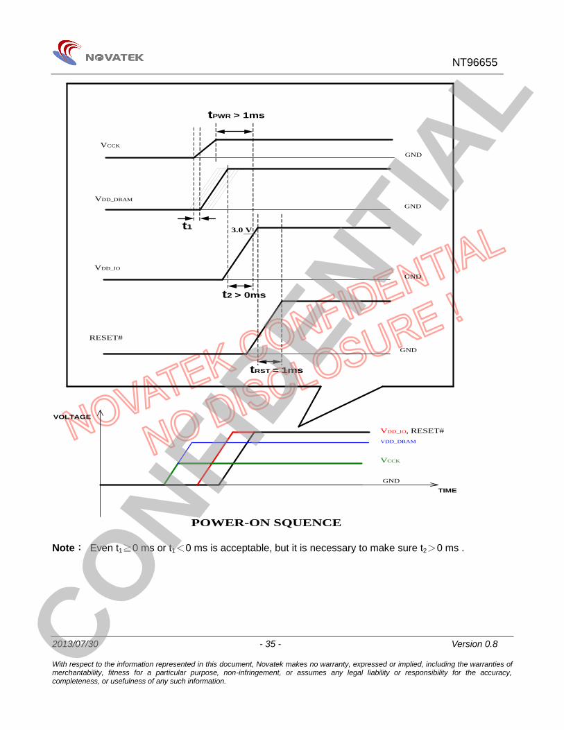
51 Power on Sequence Symbol Parameter Min Typ Max Unit Conditions
Power on sequence and Reset TRST RESET sustained time 1 - - ms after power being stable
TPWR Core power prior to IO power time 1 - - ms
CONFIDEN
TIAL
NT96655
20130730 - 35 - Version 08 With respect to the information represented in this document Novatek makes no warranty expressed or implied including the warranties of merchantability fitness for a particular purpose non-infringement or assumes any legal liability or responsibility for the accuracy completeness or usefulness of any such information
POWER-ON SQUENCE
VCCK
VDD_DRAM
VDD_IO
RESET
t1
GND
GND
30 V
GND
tPWR gt 1ms
GND
tRST = 1ms
GND
VDD_IO RESETVDD_DRAM
VCCK
VOLTAGE
TIME
t2 gt 0ms
Note Even t1≧0 ms or t1<0 ms is acceptable but it is necessary to make sure t2>0 ms
CONFIDEN
TIAL
NT96655
20130730 - 36 - Version 08 With respect to the information represented in this document Novatek makes no warranty expressed or implied including the warranties of merchantability fitness for a particular purpose non-infringement or assumes any legal liability or responsibility for the accuracy completeness or usefulness of any such information
POWER-OFF SEQUENCE
VCCK
VDD_DRAM
VDD_IO
RESET
GND
GND
GND
t6gt 0ms
GND
GND
VDD_DRAM
VCCK
VOLTAGE
TIME
t5gt 0ms
t4gt 0ms
Note Novatek recommends that t4>0 ms t5>0 ms and t6>0 ms for a stable system application But they
are not the required restrictions for Novatekrsquos DSP CONFIDEN
TIAL
NT96655
20130730 - 37 - Version 08 With respect to the information represented in this document Novatek makes no warranty expressed or implied including the warranties of merchantability fitness for a particular purpose non-infringement or assumes any legal liability or responsibility for the accuracy completeness or usefulness of any such information
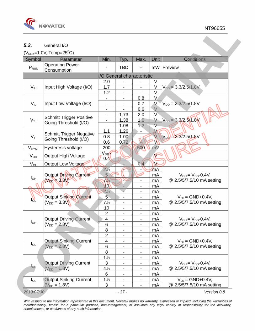
52 General IO (VDDK=10V Temp=250C) Symbol Parameter Min Typ Max Unit Conditions
PRUN Operating Power Consumption - TBD -- mW Preview
IO General characteristic 20 - - V 17 - - V VIH Input High Voltage (IO) 12 - - V
VDD = 332518V
- - 08 V - - 07 V VIL Input Low Voltage (IO) - - 06 V
VDD = 332518V
- 173 20 V - 138 16 V VT+
Schmitt Trigger Positive Going Threshold (IO) - 108 12 V
VDD = 332518V
11 126 - V 08 100 - V VT-
Schmitt Trigger Negative Going Threshold (IO) 06 072 - V
VDD = 332518V
VHYST Hysteresis voltage 200 - 500 mV
VOH Output High Voltage VDD - 04 - - V
VOL Output Low Voltage - - 04 V 25 - - mA 5 - - mA
75 - - mA IOH Output Driving Current (VDD = 33V)
10 - - mA
VOH = VDD-04V 2557510 mA setting
25 - - mA 5 - - mA
75 - - mA IOL Output Sinking Current (VDD = 33V)
10 - - mA
VOL = GND+04V 2557510 mA setting
2 - - mA 4 - - mA 6 - - mA IOH Output Driving Current
(VDD = 28V) 8 - - mA
VOH = VDD-04V 2557510 mA setting
2 - - mA 4 - - mA 6 - - mA IOL
Output Sinking Current (VDD = 28V)
8 - - mA
VOL = GND+04V 2557510 mA setting
15 - - mA 3 - - mA
45 - - mA IOH Output Driving Current (VDD = 18V)
6 - - mA
VOH = VDD-04V 2557510 mA setting
15 - - mA IOL Output Sinking Current (VDD = 18V) 3 - - mA
VOL = GND+04V 2557510 mA setting CONFI
DENTI
AL
NT96655
20130730 - 38 - Version 08 With respect to the information represented in this document Novatek makes no warranty expressed or implied including the warranties of merchantability fitness for a particular purpose non-infringement or assumes any legal liability or responsibility for the accuracy completeness or usefulness of any such information
45 - - mA 6 - - mA
IILeakage Input Leakage Current -10 plusmn1 +10 uA GND le VIN le VDD input wo RPURPD
IHIZ Output Tri-state Leakage Current -10 plusmn1 +10 uA
5 - - mA 10 - - mA 15 - - mA IOH Output Driving Current
(VDD = 33V) 20 - - mA
VOH = VDD-04V 5101520 mA setting
5 - - mA 10 - - mA 15 - - mA IOL
Output Sinking Current (VDD = 33V)
20 - - mA
VOL = GND+04V 5101520 mA setting
IOH Output Driving Current 4 - - mA VOH = VDD-04V CONFIDEN
TIAL
NT96655
20130730 - 39 - Version 08 With respect to the information represented in this document Novatek makes no warranty expressed or implied including the warranties of merchantability fitness for a particular purpose non-infringement or assumes any legal liability or responsibility for the accuracy completeness or usefulness of any such information
8 - - mA 12 - - mA
(VDD = 28V)
16 - - mA
5101520 mA setting
4 - - mA 8 - - mA 12 - - mA IOL
Output Sinking Current (VDD = 28V)
16 - - mA
VOL = GND+04V 5101520 mA setting
3 - - mA 6 - - mA 9 - - mA IOH Output Driving Current
(VDD = 18) 12 - - mA
VOH = VDD-04V 5101520 mA setting
3 - - mA 6 - - mA 9 - - mA IOL
Output Sinking Current (VDD = 18)
12 - - mA
VOL = GND+04V 5101520 mA setting
IOs2 (strong drivingsinking output capacity) 125 - - mA 15 - - mA
175 - - mA IOH Output Driving Current (VDD = 33V)
20 - - mA
VOH = VDD-04V 5101520 mA setting
125 - - mA 15 - - mA
175 - - mA IOL Output Sinking Current (VDD = 33V)
20 - - mA
VOL = GND+04V 5101520 mA setting
IOss (double strong drivingsinking output capacity) 125 - - mA 15 - - mA
175 - - mA 20 - - mA 25 - - mA - 30 - mA - 35 - mA
IOH Output Driving Current (VDD = 33V)
- 40 - mA
VOH = VDD-04V
125 - - mA 15 - - mA
175 - - mA 20 - - mA 25 - - mA - 30 - mA - 35 - mA
20130730 - 40 - Version 08 With respect to the information represented in this document Novatek makes no warranty expressed or implied including the warranties of merchantability fitness for a particular purpose non-infringement or assumes any legal liability or responsibility for the accuracy completeness or usefulness of any such information
53 Specific function IO(RTC Reset LVD and PBC) Symbol Parameter Min Typ Max Unit Conditions
RTC
TSTART_UP RTC 32768Hz crystal start up time - 250 - ms VDD_RTC=30V
IRTC Operating current of RTC - 1 - uA VDD_RTC=25V VDD_RTCO Operating voltage of RTC 15 - 36 V VDD_VBAT gt= 22V
VDD_RTCM Maintenance voltage of RTC 1 - 36 V no VDD_VBAT
RESET amp Low Voltage Detector
RPU_RST Pull-Up Resistor of RESET 80 100 130 KΩ VDD=33V
RPD_RST Pull-Down Resistor of RESET - 600 - Ω VDD=33V
VDET Detect level of LVD - 265 29 V VHYST Hysteresis voltage of LVD - 90 - mV
VPFD+ PFD Positive Going Threshold Voltage (Core power)
- 085 09 V VDD_VBAT = 22~36V
VPFD- PFD Negative Going Threshold Voltage (Core power)
075 08 - V VDD_VBAT = 22~36V
IPD1 Pull-Down Current (PWR_SW1) - 10 - uA VDD_RTC=30V
IPU2 Pull-Up Current (PWR_SW2) - 10 - uA VDD_RTC=30V
IPD3 Pull-Down Current (PWR_SW3) - 3 - uA VDD_RTC=30V
IPD4 Pull-Down Current (PWR_SW4) - 1 - uA VDD_RTC=30V
ROH Resistor of PWR_EN Output High 1100 1300 1500 Ω VOH=29V VDD_RTC=33V
ROL Resistor of PWR_EN 180 250 220 Ω VOL=04V VDD_RTC=33V CONFIDEN
TIAL
NT96655
20130730 - 41 - Version 08 With respect to the information represented in this document Novatek makes no warranty expressed or implied including the warranties of merchantability fitness for a particular purpose non-infringement or assumes any legal liability or responsibility for the accuracy completeness or usefulness of any such information
Output Low
VOH PWR_EN Output High Voltage
VBAT - 02 - - V IOH = 100uA
VOL PWR_EN Output Low Voltage - - 01 V IOL = -100uA
Note Symbol Parameter Min Typ Max Unit Conditions REN-CL PWR_EN Current Limit resistor - 1K - Ohm VOH PWR_EN Output High Voltage VBAT - 02 - - V IOH = 100uA VOL PWR_EN Output Low Voltage - - 01 V IOL = -100uA
REN-CL PWR_EN Current Limit resistor - 1K - Ohm
54 DRAM Symbol Parameter Min Typ Max Unit Conditions
DDRII DRAM DC specification
VREF DRAM IO Reference Voltage
049 VDD_DR - 051
VDD_DR V
VIH(DC) DRAM IO DC Input High (Logic 1) Voltage
VREF +0125 - VDD_DR
+03 V
VIL(DC) DRAM IO DC Input Low (Logic 0) Voltage -03 - VREF
-0125 V
VIH(AC) DRAM IO AC Input High (Logic 1) Voltage
VREF +0250 - - V
VIL(AC) DRAM IO AC Input Low (Logic 0) Voltage - - VREF
-0250 V
IOH DRAM IO Output Driving Current 46 - - mA
IOL DRAM IO Output Sinking Current 46 - - mA
IILeakage Input Leakage Current - - plusmn2 uA GND le VIN le VDD input wo RPURPD
Differential input logic Level
VIN(DC) DC differential signal voltage -03 - VDD_DR
+03 V
VID(DC) DC differential input voltage 025 - VDD_DR
+06 V
VID(AC) AC differential input voltage 05 - VDD_DR
+06 V
VIX(AC) AC differential cross point voltage
05 VDD_DR -0175
- 05
VDD_DR +0175
V CONFIDEN
TIAL
NT96655
20130730 - 42 - Version 08 With respect to the information represented in this document Novatek makes no warranty expressed or implied including the warranties of merchantability fitness for a particular purpose non-infringement or assumes any legal liability or responsibility for the accuracy completeness or usefulness of any such information
VOX(AC) AC differential output cross point voltage
05 VDD_DR -0125
- 05
VDD_DR +0125
V
AC specification tCH clock high pulse width 045 05 055 tCK tCL clock low pulse width 045 05 055 tCK
DDRIII DRAM DC specification
VREF DRAM IO Reference Voltage
049 VDD_DR - 051
VDD_DR V
VIH(DC) DRAM IO DC Input High (Logic 1) Voltage
VREF +0100 - VDD_DR V
VIL(DC) DRAM IO DC Input Low (Logic 0) Voltage VSS - VREF
-0100 V
VIH(AC) DRAM IO AC Input High (Logic 1) Voltage
VREF +0175 - Note1 V
VIL(AC) DRAM IO AC Input Low (Logic 0) Voltage Note1 - VREF
-0175 V
IOH DRAM IO Output Driving Current 4 - - mA VDD_DR =15V VOH = VDD_DR-03V
IOL DRAM IO Output Sinking Current 4 - - mA VDD_DR =15V VOL = VDD_DR+03V
IILeakage Input Leakage Current - - plusmn2 uA GND le VIN le VDD input wo RPURPD
Differential input logic level
VIH(Diff) Differential input high voltage 0200 - Note2 V
VIL(Diff) Differential input low voltage Note2 - -0200 V
VIHDiff(AC) Differential input high AC voltage
2 (VIH(AC) - VREF)
- Note2 V
VILDiff(AC) Differential input low AC voltage Note2 -
2 (VREF
-VIL(AC)) V
VIX Differential input cross point relative to VDD2 for CK CK
-150 - 150 mV
AC specification tCH clock high pulse width 045 05 055 tCK tCL clock low pulse width 045 05 055 tCK
Note
1 refer to ldquoOvershoot and Undershoot Specificationsrdquo 2 These values are not defined however the single-ended signals CK CK DQS
DQS DQSL DQSL DQSU DQSU need to be within the respective limits (VIH(dc) max VIL(dc)min) for single-ended signals as well as the limitations for overshoot and undershoot Refer to ldquoOvershoot and Undershoot Specificationsrdquo CONFI
DENTI
AL
NT96655
20130730 - 43 - Version 08 With respect to the information represented in this document Novatek makes no warranty expressed or implied including the warranties of merchantability fitness for a particular purpose non-infringement or assumes any legal liability or responsibility for the accuracy completeness or usefulness of any such information
55 High speed serial interface(MIPI CSI LVDS HiSPi) Symbol Parameter Min Typ Max Unit Conditions
Input Impedance
ZID Impedance of Differential Terminator 80 100 125 Ohm (check resistorrsquos accuracy)
LVDSHiSPi(Sub-LVDSHiVCM) HS Receiver DC Specifications
VIHHS Single-ended input high voltage - - 490 mV (360+130))
VILHS Single-ended input low voltage -10 - - mV (120-130)
MIPI HS Receiver DC Specifications
VCMRX(DC) Common-mode voltage HS 70 - 330 mV Note 12
CKCK
CHt CLt
CKt
SDRDDR SDRAM clock high pulse and low
CONFIDEN
TIAL
NT96655
20130730 - 44 - Version 08 With respect to the information represented in this document Novatek makes no warranty expressed or implied including the warranties of merchantability fitness for a particular purpose non-infringement or assumes any legal liability or responsibility for the accuracy completeness or usefulness of any such information
receive mode
VIDTH Differential input high threshold - - 70 mV
VIDTL Differential input low threshold -70 - - mV
VIHHS Single-ended input high voltage - - 460 mV Note 1
1 Excluding possible additional RF interface of 100mV peak sine wave beyond 450MHz 2 This table value includes a ground difference of 50mV between the transmitter and the
receiver the static common-mode level tolerance and variation below 450MHz
MIPI LP Receiver DC specifications VIH Logic 1 input voltage 880 - - mV
VIL Logic 0 input voltage not in ULP State
- - 500 mV
VHYST Input Hysteresis 25 - - mV General Purpose Input DC specifications
1 Excluding lsquostaticrsquo ground shift of 50mV 2 ΔVCMRX(HF) is the peak amplitude of a sine wave superimposed on the receiver inputs 3 For higher bit rates a 14pF capacitor will be needed to meet the common-mode return
loss specification 4 Voltage difference compared to DC average common-mode potential
MIPI LP Receiver AC specifications CONFI
DENTI
AL
NT96655
20130730 - 45 - Version 08 With respect to the information represented in this document Novatek makes no warranty expressed or implied including the warranties of merchantability fitness for a particular purpose non-infringement or assumes any legal liability or responsibility for the accuracy completeness or usefulness of any such information
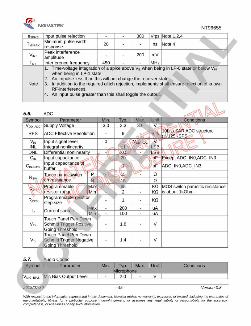
1 Time-voltage integration of a spike above VIL when being in LP-0 state or below VIH when being in LP-1 state
2 An impulse less than this will not change the receiver state 3 In addition to the required glitch rejection implements shall ensure rejection of known
RF-interferences 4 An input pulse greater than this shall toggle the output
56 ADC Symbol Parameter Min Typ Max Unit Conditions VDD_ADC Supply Voltage 30 33 36 V
RES ADC Effective Resolution - 9 - Bits 10bits SAR ADC structure (≦125KSPS
CIN-buffer Input capacitance of buffer - 1 - pF ADC_IN0ADC_IN3
P - 15 - Ω RSW Touch panel switch
on resistance N 15 Ω Max - 65 - KΩ RPU Programmable
resistor range Min - 2 - KΩ MOS switch parasitic resistance is about 1kOhm
RRPS Programmable resistor step size - 1 - KΩ
Max - 200 - uA IP Current source Min - 100 - uA
VT+ Touch Panel Pen Down Schmitt Trigger Positive Going Threshold
- 18 - V
VT- Touch Panel Pen Down Schmitt Trigger Negative Going Threshold
- 14 - V
57 Audio Codec Symbol Parameter Min Typ Max Unit Conditions
Microphone VMIC_BIAS Mic Bias Output Level - 20 - V CONFI
DENTI
AL
NT96655
20130730 - 46 - Version 08 With respect to the information represented in this document Novatek makes no warranty expressed or implied including the warranties of merchantability fitness for a particular purpose non-infringement or assumes any legal liability or responsibility for the accuracy completeness or usefulness of any such information
VIN Input Full Scale Level - 1 - Vp-p 0dB gain SNR Signal to Noise Ratio - 68 - dBA 0dB gain A-weighting
THD+N Total Harmonic Distortion Plus Noise Ratio - -65 - dBA 0dB gain A-weighting
- 238 - KΩ PGA gain set to +255 dB - 24 - KΩ PGA gain set to 0 dB RIN Input Resistance - 442 - KΩ PGA gain set to -21 dB
GPGA Programmable Gain Amplifier Range -21 - +255 dB 32 steps
GSTEP Programmable Gain Amplifier Step Size - 15 - dB
GBoost Boost Gain - 20 - dB 0101520 dB Headphone or Line Out
VOUT Line output full scale - 0698 - VRMS SNR Signal to noise ratio - 85 - dBA
THD+N Total harmonic distortion plus noise ratio - -80 - dBA
Speaker BTL Output 8Ω SNR Signal to Noise Ratio - 90 - dB A-weighting
THD+N Total Harmonic Distortion Plus Noise Ratio - TBD - dB A-weighting
GPGA Programmable Gain Amplifier Range -316 - +6 dB 32 steps
GSTEP Programmable Gain Amplifier Step Size - 117 - dB
VCODE Out Voltage-DAC Code 1023 - 128 - V Rload = 375 Ohm
VLE Video Level Error -5 - +5
VOC Output Compliance Range 0 - 14 V
FCLK Conversion rate - 27 - MHz CONFIDEN
TIAL
NT96655
20130730 - 47 - Version 08 With respect to the information represented in this document Novatek makes no warranty expressed or implied including the warranties of merchantability fitness for a particular purpose non-infringement or assumes any legal liability or responsibility for the accuracy completeness or usefulness of any such information
59 MIPI DSI Tx Symbol Parameter Min Typ Max Unit Conditions
MIPI D-PHY DC specifications HS Transmitter
VCMTX HS transmit static common mode voltage 150 200 250 mV Note 1
|ΔVCMTX
(10)|
VCMTX mismatch when output is Differential-1 or Differential-0
|ΔVOD| VOD mismatch when output is Differential-1 or Differential-0
- - 10 mV Note 2
VOHHS HS output high voltage 360 mV Note 1
ZOS Single ended output impedance 40 50 625 Ω
ΔZOS Single ended output impedance Mismatch
- - 10
Note
1 Value when driving into load impedance anywhere in the ZID range 2 It is recommended the implementer minimize ΔVOD and ΔVCMTX (10) in order to minimize
1 See Figure 42 and Figure 43 in MIPI D-PHY specification 2 Though no maximum value for ZOLP is specified the LP transmitter output impedance
shall ensure the TRLPTFLP specification is met
LP Receiver VIH Logic 1 input voltage 880 - - mV
VIL Logic 0 input voltage not in ULP State
- - 500 mV
VIL_ULPS Logic 0 input voltage ULP State - - 300 mV
VHYST Input Hysteresis 25 - - mV
Note
1 See Figure 42 and Figure 43 in MIPI D-PHY specification 2 Though no maximum value for ZOLP is specified the LP transmitter output impedance
shall ensure the TRLPTFLP specification is met CONFI
DENTI
AL
NT96655
20130730 - 48 - Version 08 With respect to the information represented in this document Novatek makes no warranty expressed or implied including the warranties of merchantability fitness for a particular purpose non-infringement or assumes any legal liability or responsibility for the accuracy completeness or usefulness of any such information
Contention Detector (LP-CD)
VIHCD Logic 1 contention threshold
450 - - mV
VILCD Logic 0 contention threshold
- - 200 mV
MIPI D-PHY AC specifications HS Transmitter
ΔVCMTX
(HF)
Common-level variations above 450MHz
- - 15 mV RMS
ΔVCMTX
(LF) Common-level variation between 50-450MHz - - 25 mV
PEAK
tR and tF 20-80 rise time and fall time - - 03 UI Note 1
150 - - ps
Note 1 UI is equal to 1(2fh) See section 73 for the definition of fh
LP Transmitter
TRLPTFLP 15-85 rise time and fall time - - 25 ns Note 1
TREOT 30-85 rise time and fall time - - 35 ns Note 1 5 6
TLP-PULSE-T
X
Pulse width of the LP exclusive-OR clock
First LP exclusive-ORclock pulse after Stop state or last pulse before Stop state
40 - - ns Note 4
All other pulses 20 - - ns Note 4
TLP-PER-TX Period of the LP exclusive-OR clock 90 - - ns
20130730 - 49 - Version 08 With respect to the information represented in this document Novatek makes no warranty expressed or implied including the warranties of merchantability fitness for a particular purpose non-infringement or assumes any legal liability or responsibility for the accuracy completeness or usefulness of any such information
to 70pF (Rising Edge Only)
Slew rate CLOAD = 0 to 70pF (Rising Edge Only)
30 ndash 0075 (VOINST ndash 700)
- - mVns Note 1 10 11
CLOAD Load capacitance 0 - 70 pF Note 1
Note
1 CLOAD includes the low-frequency equivalent transmission line capacitance The capacitance of TX and RX are assumed to always be lt10pF The distributed line capacitance can be up to 50pF for a transmission line with 2ns delay
2 When the output voltage is between 400 mV and 930 mV 3 Measured as average across any 50 mV segment of the output signal transition 4 This parameter value can be lower than TLPX due to differences in rise vs fall signal
slopes and trip levels and mismatches between Dp and Dn LP transmitters Any LP exclusive-OR pulse observed during HS EoT (transition from HS level to LP-11) is glitch behavior as described in section 822
5 The rise-time of TREOT starts from the HS common-level at the moment the differential amplitude drops below 70mV due to stopping the differential drive
6 With an additional load capacitance CCM between 0 and 60pF on the termination center tap at RX side of the Lane
7 This value represents a corner point in a piecewise linear curve See Figure 45 and Figure 46
8 When the output voltage is in the range specified by VPIN(absmax) 9 When the output voltage is between 400 mV and 700 mV 10 Where VOINST is the instantaneous output voltage VDP or VDN in millivolts 11 When the output voltage is between 700 mV and 930 mV
1 Time-voltage integration of a spike above VIL when being in LP-0 state or below VIH when being in LP-1 state
2 An impulse less than this will not change the receiver state 3 In addition to the required glitch rejection implements shall ensure rejection of known
RF-interferences 4 An input pulse greater than this shall toggle the output
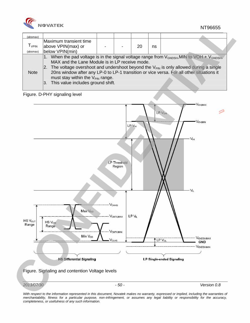
Pin Characteristic Specifications VPIN Pin signal voltage range -50 - 1350 mV ILEAK Pin leakage current -10 - 10 uA
VGNDSH Ground shift -50 - 50 mV VPIN Transient pin voltage level -015 - 145 V CONFI
DENTI
AL
NT96655
20130730 - 50 - Version 08 With respect to the information represented in this document Novatek makes no warranty expressed or implied including the warranties of merchantability fitness for a particular purpose non-infringement or assumes any legal liability or responsibility for the accuracy completeness or usefulness of any such information
(absmax)
TVPIN
(absmax)
Maximum transient time above VPIN(max) or below VPIN(min)
- - 20 ns
Note
1 When the pad voltage is in the signal voltage range from VGNDSHMIN to VOH + VGNDSH MAX and the Lane Module is in LP receive mode
2 The voltage overshoot and undershoot beyond the VPIN is only allowed during a single 20ns window after any LP-0 to LP-1 transition or vice versa For all other situations it must stay within the VPIN range
3 This value includes ground shift
Figure D-PHY signaling level
Figure Signaling and contention Voltage levels CONFIDEN
TIAL
NT96655
20130730 - 51 - Version 08 With respect to the information represented in this document Novatek makes no warranty expressed or implied including the warranties of merchantability fitness for a particular purpose non-infringement or assumes any legal liability or responsibility for the accuracy completeness or usefulness of any such information
510 HDMI Tx Symbol Parameter Min Typ Max Unit Conditions
Transmitter DC Specifications
VOFF Single-ended standby output voltage 3125 33 3475 V
VSWING Single-ended output swing voltage 400 500 600 mV
VH Single-ended high level output voltage 2935 33 3475 V
VL Single-ended low level output voltage 2435 28 3065 V
Transmitter AC Specifications Risefall time 75 - - ps
Intra-Pair Skew at source connector - - 015 Tbit
Inter-Pair Skew at source connector - - 020 Tchar
Clock duty cycle 40 50 60
TMDS Differential Clock Jitter - - 025 Tbit
Hot Plug Detection Signal
VIH Input High Voltage (HDMI_PLUG) 20 - - V Max 53V
VIL Input Low Voltage - - 08 V CONFIDEN
TIAL
NT96655
20130730 - 52 - Version 08 With respect to the information represented in this document Novatek makes no warranty expressed or implied including the warranties of merchantability fitness for a particular purpose non-infringement or assumes any legal liability or responsibility for the accuracy completeness or usefulness of any such information
(HDMI_PLUG) Note
511 USB Symbol Parameter Min Typ Max Unit Conditions
High Speed DC Specifications Input Levels (differential receiver)
VHSDIFF High speed differential input sensitivity 300 - - mV |VI(DP)-VI(DM)| measured at the
connection as application circuit
VHSCM High speed data signaling common mode voltage range
-50 - 500 mV
- - 100 mV squelch detected VHSSQ High speed squelch detection threshold 150 - - mV no squelch detected
625 - - mV disconnection detected VHSDSC High speed disconnection detection threshold - - 525 mV disconnection not detected
Output Levels
VHSOI High speed idle level output voltage (differential)
-10 - 10 mV
VHSOL High speed low level output voltage (differential)
-10 - 10 mV
VHSOH High speed high level output voltage (differential)
-360 - 400 mV
VCHRPJ Chirp-J output voltage (differential) 700 - 1100 mV
VCHIRPK Chirp-K output voltage (differential) -900 - -500 mV
Resistance
3 6 9 Ω equivalent resistance used as internal chip only RDRV Driver output impedance
405 45 495 Ω overall resistance including external resistor
Termination
VTERM Termination voltage for pull-up resistor on pin RPU
30 - 36 V
Full Speed DC Specifications Input Levels (differential receiver)
VDI Differential input sensitivity 02 - - V |VI(DP)-VI(DM)|
VCM Differential common mode voltage 08 - 25 V
Input Levels (single-ended receivers) CONFIDEN
TIAL
NT96655
20130730 - 53 - Version 08 With respect to the information represented in this document Novatek makes no warranty expressed or implied including the warranties of merchantability fitness for a particular purpose non-infringement or assumes any legal liability or responsibility for the accuracy completeness or usefulness of any such information
VSE Single ended receiver threshold 08 - 20 V
Output Levels VOL Low-level output voltage 0 - 03 V VOH High-level output voltage 28 - 36 V
High Speed AC Specifications Driver Characteristics
THSDRATE High speed TX data rate 47976 - 48024 Mbps THSRDRATE High speed RX data rate 47976 - 48024 Mbps
tHSR High speed differential rise time 500 - - ps
tHSF High speed differential fall time 500 - - ps
Driving timing
Driver waveform requirement see eye pattern of template 1 Follow template1 described in
USB20 spec Receiver timing
Data source jitter and receiver jitter tolerance see eye pattern of template 4 Follow template 4 described in
USB20 spec Full Speed AC Specifications
Driver Characteristics TFSDRATE Full speed TX data rate 11994 - 12006 Mbps TFSRDRATE Full speed RX data rate 1197 - 1203 Mbps
tFR Rise time 4 - 20 ns CL=50pF 10 to 90 of |VOH-VOL|
tFF Fall time 4 - 20 ns CL=50pF 90 to 10 of |VOH-VOL|
tFRMA Differential risefall time matching (tFRtFF)
90 - 110 Excluding the first transition from idle mode
VCRS Output signal crossover voltage 13 - 20 V Excluding the first transition
from idle mode Driving timing
VI FSE0 OE to DP DN propagation delay - - 15 ns
for detailed description of VI FSE0 and OE please refer to USB11 spec
TFDEOP Source jitter for differential transition to SE0 transition -2 - 5 ns
TJR1 Receiver jitter -185 - 185 ns To next transition TJR2 Receiver jitter -9 - 9 ns For paired transition
TFEOPT Source SE0 interval of EOP 160 - 175 ns
TFEOPR Receiver SE0 interval of EOP 82 - - ns
TFST Width of SE0 interval during differential transition
- - 14 ns CONFIDEN
TIAL
NT96655
20130730 - 54 - Version 08 With respect to the information represented in this document Novatek makes no warranty expressed or implied including the warranties of merchantability fitness for a particular purpose non-infringement or assumes any legal liability or responsibility for the accuracy completeness or usefulness of any such information
Receiver timing tPLH(RCV) tPHL(RCV)
Receiver propagation delay (DP DM to RCV) - - 15 ns for detailed description of RCV
please refer to USB11 spec
tPLH(single) tPHL(single)
Receiver propagation delay (DP DM to VOP VON)
- - 15 ns
Note
Vbus D + D -
GND
Test Supply Voltage
143 Ohm
143 Ohm
+
-
To 50 Ohm Inputs of a High speed Differential Oscilloscope
USB Connector
nearest Device Under Test
158 Ohm
158 Ohm
Differential Data Lines 10
90 10
90
HSRt HSFt
High speed Data Signal Rise and Fall time
CONFIDEN
TIAL
NT96655
20130730 - 55 - Version 08 With respect to the information represented in this document Novatek makes no warranty expressed or implied including the warranties of merchantability fitness for a particular purpose non-infringement or assumes any legal liability or responsibility for the accuracy completeness or usefulness of any such information
Differential Data Lines
Full speed Output Signal Crossover Voltage
TxD+
TxD-
SR
SR LC
LC
Full-speed
CRSV CRSV
Differential Data Lines 10
90 10
90
FRt FFt
Full speed Data Signal Rise and Fall time
TxD+
TxD-
SR
SR LC
LC
Full-speed
CONFIDEN
TIAL
NT96655
20130730 - 56 - Version 08 With respect to the information represented in this document Novatek makes no warranty expressed or implied including the warranties of merchantability fitness for a particular purpose non-infringement or assumes any legal liability or responsibility for the accuracy completeness or usefulness of any such information
512 USB Charging Port Detect Symbol Parameter Min Typ Max Unit Conditions VDAT_REF Data Detect Voltage 025 - 04 V VDM_SRC D- Source Voltage 05 - 07 V VDP_SRC D+ Source Voltage 05 - 07 V
VLGC Logic Threshold 08 - 20 V VLGC_HI Logic High 20 - 36 V
VLGC_LOW Logic Low 0 - 08 V IDM_SINK D- Sink Current 25 - 175 uA IDP_SINK D+ Sink Current 25 - 175 uA
IDP_SRC Data Contact Detect Current Source 7 - 13 uA
RDM_DWN D- Pull-down resistance 1425 - 248 kΩ
CONFIDEN
TIAL
NT96655
20130730 - 2 - Version 08 With respect to the information represented in this document Novatek makes no warranty expressed or implied including the warranties of merchantability fitness for a particular purpose non-infringement or assumes any legal liability or responsibility for the accuracy completeness or usefulness of any such information
20130730 - 3 - Version 08 With respect to the information represented in this document Novatek makes no warranty expressed or implied including the warranties of merchantability fitness for a particular purpose non-infringement or assumes any legal liability or responsibility for the accuracy completeness or usefulness of any such information
51 Power on Sequence34 52 General IO37 53 Specific function IO(RTC Reset LVD and PBC) 40 54 DRAM41 55 High speed serial interface(MIPI CSI LVDS HiSPi) 43 56 ADC 45 57 Audio Codec45 58 TV encoder46 59 MIPI DSI Tx 47 510 HDMI Tx51 511 USB 52 512 USB Charging Port Detect 56
CONFIDEN
TIAL
Administrator
打字机
深圳睿鹰科技有限公司
NT96655
20130730 - 4 - Version 08 With respect to the information represented in this document Novatek makes no warranty expressed or implied including the warranties of merchantability fitness for a particular purpose non-infringement or assumes any legal liability or responsibility for the accuracy completeness or usefulness of any such information
Revision History Rev Date Author Contents 01 20120213 Kevin Hung First draft version 02 20120316 Kevin Hung For PM 03 20120907 Kevin Hung Add pin number amp DDR_PHY(DLL) power issue (ES version)
04 20120928 Kevin Hung
Change AVDD_MPLL10V 15V Exchange function pin-out about SN_SHUTTER and SN_FLASH Exchange Microphone R-ch and L-ch Remove HV description 1 Update GPIO pull updown spec 2 Change RESET HIS IOz pull updown resistor symbol 3 Add IOSS driving and pull updown DC characteristics 4 Add IOs2 driving spec 5 Change IO 25V spec to 28V spec 6 Add RESET pin Schmitt trigger level spec
05 20121129 Roy Lo
7 change TV_RADJrsquos resistor 470430 Ohm 05 20121220 Roy Lo Update DDRIII IO drivingsinking spec 05 20130118 Kevin Hung Remove DR_CS modify N4K3 pin define for Ver AB 05 20130311 Joel Update CPU amp DRAM max operating frequency 06 20130513 Kevin Hung Modify default status of MC14 internal resistor from pu pd 06 20130514 Kevin Hung Exchange N4K3 pin define for Ver BC 07 20130614 Kevin Hung Add NT96656 in this common version 08 20130730 Kevin Hung Separate from common version
CONFIDEN
TIAL
Administrator
打字机
深圳睿鹰科技有限公司
NT96655
20130730 - 5 - Version 08 With respect to the information represented in this document Novatek makes no warranty expressed or implied including the warranties of merchantability fitness for a particular purpose non-infringement or assumes any legal liability or responsibility for the accuracy completeness or usefulness of any such information
Features High Performance 32-bit CPU
MIPS32 24Kec with ASE DSP extension MMU embedded 16KB instruction and 16KB data cache Embedded ICE makes firmware debugging easier CPU operating frequency up to 432MHz on the fly programmable
Power Management Features Firmware configurable operating frequency of each functional block to meet best power
Scalable Memory Bus Architecture 16-bit DDR2 DDR3 SDRAM bus supporting up to 2Gb DDR SDRAM DRAM operating frequency up to 373MHz without ODT Tunable DDR frequency on the fly for power saving
Sensor Interface Engine Support up to 50M pixels CCDCMOS image sensor Support high speed serial interface like sub-LVDSMipiHiSPi up to 10 channels for most
commercial CMOS sensors including Sony Panasonic Aptina Samsung Sharp and Omnivision etc (8 channels for dual MIPI version)
Support parallel sensor interface for most commercial CCD sensors including Sony Panasonic Sharp and CMOS sensors including Aptina and Omnivision
Support BT601656 video input Support dual sensors input (dual MIPI version only) Support 12-bit (serial) sensor data input Support high speed serial interface sensor pixel rate up to 576MPixelssec Support continuous shot up to 10 fps for 16MP sensor Support parallel interface sensor pixel clock up to 108MHz Support movie CCD and horizontal division CCD of SONY CONFI
DENTI
AL
Administrator
打字机
深圳睿鹰科技有限公司
NT96655
20130730 - 6 - Version 08 With respect to the information represented in this document Novatek makes no warranty expressed or implied including the warranties of merchantability fitness for a particular purpose non-infringement or assumes any legal liability or responsibility for the accuracy completeness or usefulness of any such information
Support multiple field line interleaved CCD of Sharp Support smear reduction for CCD sensor Built-in color pattern generation Sensor black level clamping Efficient defect concealment algorithm Raw image sub-sample for video amp high ISO image Flexible image analysis flow for AE AWB and AF purpose Programmable histogram analysis Automatic flicker detection RGB Gamma LUT for sensor linearization correction In-pipeline lens shading compensation technology In-pipeline color shading compensation technology In-pipeline geometric distortion correction technology In-pipeline color aberration correction technology Support CMOS sensor spatial crosstalk cancellation Support in-frame dark frame subtraction with smart defect detection algorithm Support rolling shutter correction for CMOS sensor Mechanical shutter control Flash light control
Image Processing Engine Proprietary advanced anti-alias Bayer CFA color interpolation Flexible edge rendering control and enhancement Powerful noise reduction technology for still and video recording Support motion compensated temporal filtering (MCTF) for efficient video noise reduction Support temporal noise reduction with ghost reduction RGB Gamma LUT High precision color correction matrix for sRGB or specific color requirement Brightnesscontrast and huesaturation adjustment Specific color control technology (Patent) 3D color conversion for specific color preference tuning False color suppression Support wide dynamic range (WDR) for local illumination enhancement
Image Manipulation Engine High quality scaling engine for seamless digital zooming from 116x to 16x CONFI
DENTI
AL
Administrator
打字机
睿鹰-高品质行车记录仪专家
NT96655
20130730 - 7 - Version 08 With respect to the information represented in this document Novatek makes no warranty expressed or implied including the warranties of merchantability fitness for a particular purpose non-infringement or assumes any legal liability or responsibility for the accuracy completeness or usefulness of any such information
Support thumbnail image generation Forwardinverse color space transform
Face Detection Engine Very high speed face detection and tracking High accuracy under different light source Programmable target data base
Digital Image Stabilizer Remove unintended hand movement from an image sequence Single frame compensation for video (Total compensation) Accumulate frame compensation for video (Smart compensation) Motion refresh rate 60Hz
Interface search range up to 32 Programmable total compensation range Accommodate resolution 1080p Adjustable number of motion vectors for motion estimation Maximum 1024 motion vectors
per process (16 regions x 64 blocksregion)
LCDTV Display Support dual display including LCD panel and HDMITV display simultaneously High performance scaling updown engine programmable gamma correction color
transform and color management for LCD or TV display Separate OSD for LCD panel and TV Support digital LCD interface for AUO Casio CMI (all digital panels will be supported) Support 16-bit RGB parallel interface (RGB565 or Delta RGB) LCD panel up to 1024x1024
resolution Support MIPI DSI for mobile display Support 90∘rotationflipmirror
Support PAL NTSC video encoder (CVBS format) Integrated 1 internal 10-bit video DACs Support digital interface BT6016561120 output port 33V 18V LCD Digital video out
HDMI Support HDMI v13a Support DDC with maximum 100khz access rate for CEA-861-D format Support CEC CONFI
DENTI
AL
Administrator
打字机
睿鹰-高品质行车记录仪专家
NT96655
20130730 - 8 - Version 08 With respect to the information represented in this document Novatek makes no warranty expressed or implied including the warranties of merchantability fitness for a particular purpose non-infringement or assumes any legal liability or responsibility for the accuracy completeness or usefulness of any such information
Support 16 bits PCM 32 KHz 441 KHz 48KHz for maximum 2 channels audio output
Graphic Engine Copy and paste Geometric operation including mirror flip and rotation Arithmetic operation including addition subtraction color keying logic operation and alpha
blending Support warping function Support anti-alias affine transform Support hardware acceleration for multi-frame processing
Cipher 64-bit DES 3DES and AES-128 Both encryption and decryption Big and little endian of input data
H264AVC CODEC Support encoder BPMP level 41 Support encoder HP level 42 Support real-time capability for 1080p30 720p60 480p120 Support full frame still capture while video recording H264 highmain profile 1 reference picture for P-frame 2 reference pictures for B-frame Support video format MP4 AVI MOV Support bit rate control Automatic frame sync for high frame rate
Motion Estimation [-12475+12475] search range in horizontal component [-2875 +2875] search range in vertical component MB mode 16x16 16x8 8x16 8x8 skip and direct (B-frame)
FW Audio CODEC AAC encode decode (32KHz 48KHz 192kbps) ADPCM encode decode Noise cancellation for background noise motor operation and wind
20130730 - 9 - Version 08 With respect to the information represented in this document Novatek makes no warranty expressed or implied including the warranties of merchantability fitness for a particular purpose non-infringement or assumes any legal liability or responsibility for the accuracy completeness or usefulness of any such information
JPEG CODEC Supports Motion JPEG 30fps1080P30 video clipplayback function Max pixel clock 120Mpixel sec Support ISOIEC 10918-1 baseline JPEG compressiondecompression Still image maximum resolutions will be up to 65536x65536 pixels Support input format 422 420 411 400 211 JPEG supports downloadable Quantization and Huffman tables Support Exchangeable Image File format (EXIF 223 and newer) Support MPO file format for 3D image
Digital Audio Interface Support I2S codec interface Audio clock generator
Dual Graphic-based OSD Support 8-bit palette and ARGB(4565 or 8565) OSD architecture 256 colors simultaneously out of true color at 8-bit palette OSD 8 levels of opacity for 8-bit palette OSD Programmable width amp height to meet LCDTVs resolution exactly Picture in picture function Dedicated 16 face frames for face detection function
Storage Memory Controller Secure Digital card and SDIO Support SD 30 Support UHS-I UHS50 UHS104 (Max freq 108MHz) Support eMMC and hot boot Support eyeFi for wireless connection Multi-Media card SLC NAND type flash
USB Fully compliant with USB20 devicehost High speed (480Mbps) supported CONFI
DENTI
AL
Administrator
打字机
QQ848478751
Administrator
打字机
NT96655
20130730 - 10 - Version 08 With respect to the information represented in this document Novatek makes no warranty expressed or implied including the warranties of merchantability fitness for a particular purpose non-infringement or assumes any legal liability or responsibility for the accuracy completeness or usefulness of any such information
Optionally switchable to be fully compliant with USB 11 Support Control Isochronous Interrupt and Bulk transfer Support PC camera mode
Timers RTC can be powered by separate backup battery and operating from 15V to 36V Watch dog timer 16 programmable HW timers support resolution up to 3MHz and 32 bits counter
Peripheral Interface Support I2C interface Support 20 channels PWM including built-in 16 (4 sets) pattern generators for micro-Stepping
motor control Support GPIO and flexible PWM interface with micro-stepping Support programmable 3-wired serial interface Support SPI for gyroscope reading Support UART interface Support 8 channels of 10-bit ADC with touch panel interface (2 channels) the max sample
rate up to 125 KHz per channel
On-chip Boot Strap Loader Built-in on-chip mask ROM User program can be stored in NAND-type flash and external static memory is not
necessary On-chip mask ROM can be disabled System can boot from SPI flash NAND flash memory cards eMMC and USB
Triple Voltage Power Supply 105V core logic voltage 18V 15V DDRIIDDRIII SDRAM interface voltage 33V IO interface and analog circuit voltage
Package NT96655BG 305 ball TFBGA 13x13 mm2
CONFIDEN
TIAL
Administrator
打字机
QQ848478751
Administrator
打字机
NT96655
20130730 - 11 - Version 08 With respect to the information represented in this document Novatek makes no warranty expressed or implied including the warranties of merchantability fitness for a particular purpose non-infringement or assumes any legal liability or responsibility for the accuracy completeness or usefulness of any such information
General Description NT9665xBG is a high image quality high performance power saving and cost effective digital still camera (DSC) and digital video camera (DV) controller with excellent digital still image capturing and video streaming capabilities It is targeted for the application of VGA to 50M pixel DSCDV resolutions It can be easily adapted to many high speed CMOS and conventional CCD image sensors with on chip programmable interface timing approach The controller provides sophisticated video processing methods with built-in hardware acceleration pipeline This is essential for achieving high performance for per-shot shot-to-shot and continuous shooting pictures The controller provides flexible mechanism for auto white balance auto exposure and auto-focusing in order to better tradeoff hardware and software efforts over the performance Embedded H264 video CODEC supports video recording up to full-HD 1080p30 The HDMI 13 Tx is also equipped for HDTV output Rich storage interfaces are supported to make it ideal for the storage of still pictures and video streaming data The USB20 high speed interface can uploaddownload the audiovideo data efficiently tofrom PC
CONFIDEN
TIAL
Administrator
打字机
QQ848478751
Administrator
打字机
Administrator
打字机
Administrator
打字机
NT96655
20130730 - 12 - Version 08 With respect to the information represented in this document Novatek makes no warranty expressed or implied including the warranties of merchantability fitness for a particular purpose non-infringement or assumes any legal liability or responsibility for the accuracy completeness or usefulness of any such information
Block Diagram
SENSOR PORT A
SENSOR PORT B
IMAGPROCESSOR
FHD H264CODEC
JPEGCODEC
FACE DETECTDISTORTIONCORR
SCALER
CPUMIPS32 24KEc
GRAPHICS
TVENCODER
AUDIO CODECamp I2S
HDMI 13 TX
DDR PHY
PWM
RTC WDT
I2C
NAND
SIF
SDSDIOx2
USB 20HOSTDEV UART
ADC
GPIO
MOTION ESTIMATOR
LCD
SPI
DDR DMA
BT 656BT1120
CIPHER
PLL
32768KHz
12MHzDDR23
TV
LCD PANEL
PC
WIRELESS
Wi-Fi3G4GNAND FLASH SD CARD
DRAM
LENS amp SENSOR
2nd OPTIONALSENSOR MODULE
CONFIDEN
TIAL
Administrator
打字机
QQ848478751
Administrator
打字机
Administrator
打字机
Administrator
打字机
NT96655
20130730 - 13 - Version 08 With respect to the information represented in this document Novatek makes no warranty expressed or implied including the warranties of merchantability fitness for a particular purpose non-infringement or assumes any legal liability or responsibility for the accuracy completeness or usefulness of any such information
Pin Configuration
1 TFBGA-305
CONFIDEN
TIAL
NT96655
20130730 - 14 - Version 08 With respect to the information represented in this document Novatek makes no warranty expressed or implied including the warranties of merchantability fitness for a particular purpose non-infringement or assumes any legal liability or responsibility for the accuracy completeness or usefulness of any such information
Pin No Pin Name Pin No Pin Name Pin No Pin Name Pin No Pin Name A1 DR_D9 E19 I2C_SDA K11 GND R3 DR_A0 A2 DR_D14 F1 DR_DQM0 K12 GND R17 JTAG_TRST A3 FL_TRIG F2 DR_DQM1 K13 VDDK R18 XTAL_SYSO A4 SN_DGPIO5 F3 VDD_DR K14 AVDD_HDMI R19 XTAL_SYSI A5 SN_SCK F6 SP_CLK K16 AVDD_DAC T1 DR_A5 A6 SN_VD F7 PWM6 K17 TV_FSADJ T2 DR_A3 A7 HSI_D0P F8 AVDD_HSI_K K18 HDMI_TX0P T3 DR_A6 A8 HSI_D2P F9 AVDD_HSI_RX K19 HDMI_TX0N T4 MC5 A9 HSI_D4P F10 VDD_HSI_IO L1 DR_D2 T7 MC8
20130730 - 15 - Version 08 With respect to the information represented in this document Novatek makes no warranty expressed or implied including the warranties of merchantability fitness for a particular purpose non-infringement or assumes any legal liability or responsibility for the accuracy completeness or usefulness of any such information
20130730 - 16 - Version 08 With respect to the information represented in this document Novatek makes no warranty expressed or implied including the warranties of merchantability fitness for a particular purpose non-infringement or assumes any legal liability or responsibility for the accuracy completeness or usefulness of any such information
Pin Descriptions I = input port with Schmitt trigger O = output port with normal drivingsinking IO = bi-directional port with normal drivingsinking and Schmitt input mvIO = multi voltage bi-direction port with Schmitt input HSI = high speed serial interface with multi voltage input port IOsw = bi-directional port with strong drivingsinking and wide Schmitt input range IOw = bi-directional port with wide Schmitt input range IOs = bi-directional port with strong drivingsinking IOs2 = bi-directional port with strong drivingsinking IOss = bi-directional port with strong drivingsinking IOz = bi-directional port with large pulldown resistor IO5VT = bi-directional port with normal drivingsinking and Schmitt input OD = open drain output with normal sinking IOD = bi-directional port open drain output LVD = low voltage detect function pin pu = internal pull-up pd = internal pull-down AI = analog input port AI5VT = analog 5V tolerant input port AO = analog output port AIO = analog bi-directional port H = output high L = output low P = power or ground Note means this pin has interrupted function
CONFIDEN
TIAL
NT96655
20130730 - 17 - Version 08 With respect to the information represented in this document Novatek makes no warranty expressed or implied including the warranties of merchantability fitness for a particular purpose non-infringement or assumes any legal liability or responsibility for the accuracy completeness or usefulness of any such information
1 NT96655BG 305 pins
Total 305 pins Alternative GPIO 133 pins
11 System interface (9) Pin No Name Type Reset Descriptions
R19 XTAL_SYSI AI - Crystal input for system oscillator (12MHz) R18 XTAL_SYSO AO - Output for system oscillator
B15 RESET LVD pu System Reset Connect a capacitor to ground for reset time control
J12 TESTEN I I pd Test mode enable Keep low for normal operation
R17 JTAG_TRST P_GPIO[31] IO I pu JTAG test logic reset(active low)
N14 JTAG_TMS P_GPIO[32] IO I pd JTAG test mode select
P17 JTAG_TCK P_GPIO[33] IO I pd JTAG test clock input
P18 JTAG_TDI P_GPIO[34] IO I pd JTAG test data input
P19 JTAG_TDO P_GPIO[35] IO I pd JTAG test data output
12 RTC amp Power Button Controller (7) Pin No Name Type Default Descriptions
A14 XTAL_RTCI AI - Crystal input for real time clock oscillator (32768KHz) B14 XTAL_RTCO AO - Output for real time clock oscillator C14 PWR_SW1 AI I pd Power onoff signal input (ONOFF switch use) B13 PWR_SW2 AI I pu Power onoff signal input (falling edge trigger)
H12 PWR_SW3 I5VTZ I pd Power onoff signal input (5V tolerance Input for VBUSI use)
D13 PWR_SW4 AI I pd Power onoff signal input (Bettery in use) A13 PWR_EN AO - Power enable signal output
PWR_SW can trigger interrupt (share RTC interrupt) If this pin isnrsquot used Novatek recommends connecting this pin to GND
13 DRAM interface (47) Pin No Name Type Reset Descriptions
M4 DR_RESET O - Reset signal output for DDR3 DRAM M1 DR_CLK O - M2 DR_CLK O - DRAM differential clock output
N2 DR_CKE O - DRAM clock enable CONFIDEN
TIAL
NT96655
20130730 - 18 - Version 08 With respect to the information represented in this document Novatek makes no warranty expressed or implied including the warranties of merchantability fitness for a particular purpose non-infringement or assumes any legal liability or responsibility for the accuracy completeness or usefulness of any such information
M3 DR_CAS
L3 DR_RAS N3 DR_WE
O - DRAM control signals
J4 DR_VREF AI - DRAM reference voltage input P1 DR_BA0 N1 DR_BA1 P2 DR_BA2
IO - DRAM data bus inputoutput upper byte (Each bits of upper byte may be permuted to make routing simpler)
CONFIDEN
TIAL
NT96655
20130730 - 19 - Version 08 With respect to the information represented in this document Novatek makes no warranty expressed or implied including the warranties of merchantability fitness for a particular purpose non-infringement or assumes any legal liability or responsibility for the accuracy completeness or usefulness of any such information
14 Sensor interface (33) Pin No Name Type Reset Descriptions
B7 HSI_D0N S_GPI[0]
A7 HSI_D0P S_GPI[1]
D8 HSI_D1N S_GPI[2]
C8 HSI_D1P S_GPI[3]
B8 HSI_D2N S_GPI[4]
A8 HSI_D2P S_GPI[5]
D9 HSI_D3N S_GPI[6]
C9 HSI_D3P S_GPI[7]
B9 HSI_D4N S_GPI[8]
A9 HSI_D4P S_GPI[9]
B10 HSI_CK0N S_GPI[10]
A10 HSI_CK0P S_GPI[11]
D10 HSI_D5N S_GPI[12]
C10 HSI_D5P S_GPI[13]
B11 HSI_D6N S_GPI[14]
A11 HSI_D6P S_GPI[15]
D11 HSI_D7N S_GPI[16]
C11 HSI_D7P S_GPI[17]
B12 HSI_D8N S_GPI[18]
A12 HSI_D8P S_GPI[19]
D12 HSI_D9N S_GPI[20]
C12 HSI_D9P S_GPI[21]
HSI I pd
High speed differential sensor interface and parallel interface (when sensor interface is configured as high speed differential sensor interface the clock lane should be a dedicated differential lane And each data lanes may be permuted in established group refer to below table)
CONFIDEN
TIAL
NT96655
20130730 - 20 - Version 08 With respect to the information represented in this document Novatek makes no warranty expressed or implied including the warranties of merchantability fitness for a particular purpose non-infringement or assumes any legal liability or responsibility for the accuracy completeness or usefulness of any such information
D7 SN_MCLK S_GPIO[24] mvIOs I pd Programmable Clock output for sensor
C7 SN_PXCLK S_GPIO[25] mvIOs I pd Sensor Pixel Clock Input
mvIOs I pu General serial interface 0 or Serial Peripheral Interface 3 Chip Select
A5
SN_SCK SPI3_CLK I2C_SCL P_GPIO[57]
mvIOD I pu General serial interface 0 or Serial Peripheral Interface 3 clock output I2C-BUS clock output(Open Drain IO structure)
B5
SN_DAT SPI3_DO I2C_SDA P_GPIO[58]
mvIOD I pu General serial interface 0 or Serial Peripheral Interface 3 data output I2C-BUS data input output(Open Drain IO structure)
C5 SN_DGPIO4 mvIO I pd General purpose Input output A4 SN_DGPIO5 mvIO I pd General purpose Input output
B4 SPI3_DI SN_FLASH SN_DGPIO6
mvIO I pd Serial Peripheral Interface 3 data input Flash Signal input from sensor
C4 SN_SHUTTER SN_DGPIO7 mvIO I pd Shutter signal input from sensor
Note The pin can trigger interrupt Note1 The input voltage of HSI corresponds to GVDD_SN Note2 The mvIO voltage of Sensor interface corresponds to VDD_SN
Name LVDS HiSPi MIPI CSI Parallel (12 bits) CCIR601 (16 bits) CCIR601 (8 bits) S_GPI[0] HSI_D0N I SLVS_D0N I CSI_D0N I SN_D0 I S_GPI[1] HSI_D0P I SLVS_D0P I CSI_D0P I SN_D1 I S_GPI[2] HSI_D1N I SLVS_D1N I CSI_D1N I SN_D2 I S_GPI[3] HSI_D1P I SLVS_D1P I CSI_D1P I SN_D3 I S_GPI[4] HSI_D2N I SLVS_D2N I CSI_D2N I SN_D4 I CCIR_Y0 I S_GPI[5] HSI_D2P I SLVS_D2P I CSI_D2P I SN_D5 I CCIR_Y1 I S_GPI[6] HSI_D3N I SLVS_D3N I CSI_D3N I SN_D6 I CCIR_Y2 I S_GPI[7] HSI_D3P I SLVS_D3P I CSI_D3P I SN_D7 I CCIR_Y3 I S_GPI[8] HSI_D4N I SN_D8 I CCIR_Y4 I S_GPI[9] HSI_D4P I SN_D9 I CCIR_Y5 I S_GPI[10] HSI_CK0N I SLVS_CKN I CSI_CKN I SN_D10 I CCIR_Y6 I S_GPI[11] HSI_CK0P I SLVS_CKP I CSI_CKP I SN_D11 I CCIR_Y7 I S_GPI[12] HSI_D5N I CCIR_C0 I CCIR_YC0 I S_GPI[13] HSI_D5P I CCIR_C1 I CCIR_YC1 I S_GPI[14] HSI_D6N I CCIR_C2 I CCIR_YC2 I S_GPI[15] HSI_D6P I CCIR_C3 I CCIR_YC3 I S_GPI[16] HSI_D7N I CCIR_C4 I CCIR_YC4 I S_GPI[17] HSI_D7P I CCIR_C5 I CCIR_YC5 I S_GPI[18] HSI_D8N I CCIR_C6 I CCIR_YC6 I CONFI
DENTI
AL
NT96655
20130730 - 21 - Version 08 With respect to the information represented in this document Novatek makes no warranty expressed or implied including the warranties of merchantability fitness for a particular purpose non-infringement or assumes any legal liability or responsibility for the accuracy completeness or usefulness of any such information
S_GPI[19] HSI_D8P I CCIR_C7 I CCIR_YC7 I S_GPI[20] HSI_D9N I CCIR_VD I CCIR_VD I S_GPI[21] HSI_D9P I CCIR_HD I CCIR_HD I S_GPI[24] SN_MCLK O SN_MCLK O SN_MCLK O SN_MCLK O S_GPI[25] SN_PXCLK I SN_PXCLK I S_GPI[26] SN_VD IO SN_VD IO S_GPI[27] SN_HD IO SN_HD IO SN_DGPIO4 CCIR_CLK I CCIR_CLK I
15 Memory Card interface (29) Pin No Name Type Reset Descriptions
L16 SD_CAP P - Internal Supply Voltage decoupling for SDIO interface (3318V switchable default 33V)
W3 MC0 C_GPIO[0] mvIO I pu
V4 MC1 C_GPIO[1] mvIO I pu
U4 MC2 C_GPIO[2] mvIO I pu
W4 MC3 C_GPIO[3] mvIO I pu
U6 MC4 C_GPIO[4] mvIO I pu
T4 MC5 C_GPIO[5] mvIO I pu
W5 MC6 C_GPIO[6] mvIO I pu
V6 MC7 C_GPIO[7] mvIO I pu
T7 MC8 C_GPIO[8] mvIO I pu
U5 MC9 C_GPIO[9] mvIO I pu
V5 MC10 C_GPIO[10] mvIO I pu
W6 MC11 C_GPIO[11] mvIO I pu
V7 MC12 C_GPIO[12] mvIO I pd
T8 MC13 C_GPIO[13] mvIO I pd
W7 MC14 C_GPIO[14] mvIO I pd
U7 MC15 C_GPIO[15] mvIO I pu
M19 MC16 C_GPIO[16] IOs I pd
M18 MC17 IO I pu
Memory Card interface(see below table)
CONFIDEN
TIAL
NT96655
20130730 - 22 - Version 08 With respect to the information represented in this document Novatek makes no warranty expressed or implied including the warranties of merchantability fitness for a particular purpose non-infringement or assumes any legal liability or responsibility for the accuracy completeness or usefulness of any such information
C_GPIO[17]
M17 MC18 C_GPIO[18] IO I pu
M16 MC19 C_GPIO[19] IO I pu
N19 MC20 C_GPIO[20] IO I pu
N18 MC21 C_GPIO[21] IO I pu
N16 MC22 C_GPIO[22] IOs I pd
N17 MC23 C_GPIO[23] IO I pu
N13 MC24 C_GPIO[24] IO I pu
P13 MC25 C_GPIO[25] IO I pu
M13 MC26 C_GPIO[26] IO I pu
M14 MC27 C_GPIO[27] IO I pu
Note The pin can trigger interrupt Note1 The mvIO voltage of MC0~15 corresponds to VDD_MC Note2 The IO voltage of MC16~21 corresponds to SD_CAP it could be switched between 3318V by the register Memory card interface pinmux table
Name NAND Flash SDMMCeMMC SD SPI flash SPI I2S MC0 NAND_D0 IO eMMC_D0 IO SPI_DOD0 IO MC1 NAND_D1 IO eMMC_D1 IO SPI_DID1 IO MC2 NAND_D2 IO eMMC_D2 IO SPI_CLK O MC3 NAND_D3 IO eMMC_D3 IO SPI_WPD2 IO MC4 NAND_D4 IO eMMC_D4 IO SPI_HOLDD3 IO MC5 NAND_D5 IO eMMC_D5 IO MC6 NAND_D6 IO eMMC_D6 IO MC7 NAND_D7 IO eMMC_D7 IO MC8 NAND_CS0 O SPI_CS O MC9 NAND_CS1 O eMMC_CLK O MC10 NAND_WE O MC11 NAND_RE O eMMC_CMD IO MC12 NAND_CLE O MC13 NAND_ALE O MC14 NAND_WP O MC15 NAND_RDY I MC16 SD_CLK O MC17 SD_CMD IO MC18 SD_D0 IO MC19 SD_D1 IO MC20 SD_D2 IO MC21 SD_D3 IO CONFI
DENTI
AL
NT96655
20130730 - 23 - Version 08 With respect to the information represented in this document Novatek makes no warranty expressed or implied including the warranties of merchantability fitness for a particular purpose non-infringement or assumes any legal liability or responsibility for the accuracy completeness or usefulness of any such information
MC22 SDIO_CLK O SPI_CLK O I2S_MCLK O MC23 SDIO_CMD IO SPI_CS O I2S_BCLK IO MC24 SDIO_D0 IO SPI_DI I I2S_SYNC O MC25 SDIO_D1 IO SPI_DO O I2S_DO O MC26 SDIO_D2 IO I2S_DI I MC27 SDIO_D3 IO
16 LCD interface (23) Pin No Name Type Reset Descriptions
T11 LCD0 L_GPIO[0] BS0
mvIO I pd
U11 LCD1 L_GPIO[1] BS1
mvIO I pd
W10 LCD2 L_GPIO[2] BS2
mvIO I pd
LCD Signal Bus BS20 BOOT_SRC The boot source setting description 0x0 NAND with RS ECC 0x1 Boot card (Select by BOOT_CARD) 0x2 eMMC (SDIO2_2) 0x3 USB full speed 0x4 SPI flash 0x5 USB high speed 0x6 NAND with Hamming ECC 0x7 BMC (SPI)
V10 LCD3 L_GPIO[3] BS3
mvIO I pd
LCD Signal Bus BS3 Reserved for FW(MPLL control flow) BS63 is for IC debugging setting Please keep low at reset signal rising edge
U10 LCD4 L_GPIO[4] BS4
mvIO I pd
LCD Signal Bus BS4 BOOT_CARD Boot card select 0 SD 1 SDIO (SDIO2_2)
T10 LCD5 L_GPIO[5] BS5
mvIO I pd
LCD Signal Bus BS5 EJTAG_SEL EJTAG select 0 GPIO (TRST TMS TCK TDI TDO are GPIO) 1 EJTAG
W9 LCD6 L_GPIO[6] BS6
mvIO I pd
LCD Signal Bus BS6 MPLL_CLK_SEL Select clock source of PLL 0 APLL clock output (From APLL clock) 1 Bypass APLL (From external clock)
V9 LCD7 L_GPIO[7] BS7
mvIO I pd
LCD Signal Bus BS7 EMMC_BUSWIDTH eMMC boot bus width 0 4 bits data bus 1 8 bits data bus
U9 LCD8 L_GPIO[8] mvIO I pd
T9 LCD9 L_GPIO[9] mvIO I pd
W8 LCD10 L_GPIO[10] mvIO I pd
V8 LCD11 L_GPIO[11] mvIO I pd
LCD Signal Bus
CONFIDEN
TIAL
NT96655
20130730 - 24 - Version 08 With respect to the information represented in this document Novatek makes no warranty expressed or implied including the warranties of merchantability fitness for a particular purpose non-infringement or assumes any legal liability or responsibility for the accuracy completeness or usefulness of any such information
U8 LCD12 L_GPIO[12] BS8
mvIO I pd
LCD Signal Bus BS8 EMMC_BOOTMODE eMMC boot mode 0 single rate + backward timing 1 dual rate + high speed timing
N11 LCD13 L_GPIO[13] BS9
mvIO I pd
LCD Signal Bus BS9 EMMC_DDR_DATA_ORDER eMMC DDR data order 0 Odd byte (1st byte) first 1 Even byte (2nd byte) first
M11
LCD14 L_GPIO[14] BS10
mvIO I pd
LCD Signal Bus BS10 MIPS_DEBUG_MODE_SEL Enable NT9665x enters CPU debug mode Internal CPU state will be outputted to debug port on storage interface (MC[180]) 0 Normal mode 1 CPU debug mode BS10 for IC debugging setting Please keep low at reset signal rising edge
N10 LCD15 L_GPIO[15] mvIO I pd
M10 LCD16 L_GPIO[16] mvIO I pd
P7 LCD17 L_GPIO[17] mvIO I pd
N6 LCD18 L_GPIO[18] mvIO I pd
M7 LCD19 L_GPIO[19] mvIO I pd
M6 LCD20 L_GPIO[20] mvIO I pd
N7 LCD21 L_GPIO[21] mvIO I pd
P6 LCD22 L_GPIO[22] mvIO I pd
LCD Signal Bus
Note1 The mvIO voltage of LCD interface corresponds to VDD_LCD LCD interface pinmux table
Name CCIR(8 bits) Serial RGB CCIR(16 bits) i80M68 CCIR amp RGB (secondary panel)
MPU Serial (secondary panel)
LCD0 CCIR_YC0 O RGB_D0 O CCIR_Y0 O MPU_D0 IO LCD1 CCIR_YC1 O RGB_D1 O CCIR_Y1 O MPU_D1 IO LCD2 CCIR_YC2 O RGB_D2 O CCIR_Y2 O MPU_D2 IO LCD3 CCIR_YC3 O RGB_D3 O CCIR_Y3 O MPU_D3 IO LCD4 CCIR_YC4 O RGB_D4 O CCIR_Y4 O MPU_D4 IO LCD5 CCIR_YC5 O RGB_D5 O CCIR_Y5 O MPU_D5 IO LCD6 CCIR_YC6 O RGB_D6 O CCIR_Y6 O MPU_D6 IO LCD7 CCIR_YC7 O RGB_D7 O CCIR_Y7 O MPU_D7 IO LCD8 CCIR_CLK O RGB_CLK O CCIR_CLK O MPU_TE I LCD9 CCIR_VD O RGB_VD O CCIR_VD O MPU_CS O LCD10 CCIR_HD O RGB_HD O CCIR_HD O MPU_RS O LCD11 CCIR_DE O MPU_WR O CONFI
DENTI
AL
NT96655
20130730 - 25 - Version 08 With respect to the information represented in this document Novatek makes no warranty expressed or implied including the warranties of merchantability fitness for a particular purpose non-infringement or assumes any legal liability or responsibility for the accuracy completeness or usefulness of any such information
LCD12 CCIR_C0 O MPU_RD O RGB_YC0 O LCD13 CCIR_C1 O MPU_D8 IO RGB_YC1 O MPU_SDO O LCD14 CCIR_C2 O MPU_D9 IO RGB_YC2 O MPU_SDI I LCD15 CCIR_C3 O MPU_D10 IO RGB _YC3 O MPU_CS O LCD16 CCIR_C4 O MPU_D11 IO RGB _YC4 O MPU_RS O LCD17 CCIR_C5 O MPU_D12 IO RGB _YC5 O MPU_CLK O LCD18 CCIR_C6 O MPU_D13 IO RGB _YC6 O MPU_SDIO IO LCD19 CCIR_C7 O MPU_D14 IO RGB _YC7 O MI_TE I LCD20 LCD_CS O MPU_D15 IO RGB _CLK O LCD21 LCD_CLK O MPU_D16 IO RGB _VD O LCD22 LCD_DAT O MPU_D17 IO RGB _HD O
17 PWM (20) Pin No Name Type Reset Descriptions
B3 PWM0 ME_SHUT0 P_GPIO[36]
IO I pd
C3 PWM1 ME_SHUT1 P_GPIO[37]
IO I pd
D4 PWM2 P_GPIO[38] IO I pd
D3 PWM3 P_GPIO[39] IO I pd
PWM output pin Mechanical Shutter control output Micro-stepping control module 1
E3 PWM4 P_GPIO[40] IO I pd
G7 PWM5 P_GPIO[41] IO I pd
F7 PWM6 P_GPIO[42] IO I pd
L6 PWM7 P_GPIO[43] IO I pd
PWM output pin Micro-stepping control module 2 Serial Peripheral Interface
J6 PWM8 P_GPIO[44] IO I pd
K6 PWM9 P_GPIO[45] IO I pd
K7 PWM10 P_GPIO[46] IO I pd
L7 PWM11 P_GPIO[47] IO I pd
PWM output pin Micro-stepping control module 3
C17 PWM12 P_GPIO[48] IO I pd
D16 PWM13 P_GPIO[49] IO I pd
C15 PWM14 P_GPIO[50] IO I pd
B17 PWM15 P_GPIO[51] IO I pd
PWM output pin Micro-stepping control module 4
G13 PWM16 IO I pd PWM output pin CONFIDEN
TIAL
NT96655
20130730 - 26 - Version 08 With respect to the information represented in this document Novatek makes no warranty expressed or implied including the warranties of merchantability fitness for a particular purpose non-infringement or assumes any legal liability or responsibility for the accuracy completeness or usefulness of any such information
ME_SHUT0 P_GPIO[52]
H14 PWM17 ME_SHUT1 P_GPIO[53]
IO I pd Mechanical Shutter control output
J13 PWM18 P_GPIO[54] IO I pd PWM output pin
G14 PWM19 P_GPIO[55] IO I pd PWM output pin
Name PWM M-shutter u-stepping SPI
PWM0 PWM0 O ME_SHUT0 O uSTP1_A O PWM1 PWM1 O ME_SHUT1 O uSTP1_B O PWM2 PWM2 O uSTP1_C O PWM3 PWM3 O uSTP1_D O PWM4 PWM4 O uSTP2_A O SPI3_CLK O PWM5 PWM5 O uSTP2_B O SPI3_CS O PWM6 PWM6 O uSTP2_C O SPI3_DO O PWM7 PWM7 O uSTP2_D O SPI3_DI O PWM8 PWM8 O uSTP3_A O PWM9 PWM9 O uSTP3_B O PWM10 PWM10 O uSTP3_C O PWM11 PWM11 O uSTP3_D O PWM12 PWM12 O uSTP4_A O PWM13 PWM13 O uSTP4_B O PWM14 PWM14 O uSTP4_C O PWM15 PWM15 O uSTP4_D O PWM16 PWM16 O ME_SHUT0 O PWM17 PWM17 O ME_SHUT1 O PWM18 PWM18 O PWM19 PWM19 O
18 Peripheral IO (19) Pin No Name Type Reset Descriptions
E19 I2C_SDA P_GPIO[0] IOD I pu I2C-BUS clock output(Open Drain IO structure)
F17 I2C_SCL P_GPIO[1] IOD I pu I2C-BUS data input output(Open Drain IO structure)
C19 SB_CS2 SPI3_CS P_GPIO[7]
IO I pu Serial Interface Chip Select 2 Serial Peripheral Interface 3 chip select output
C18 SB_CS3 SPI3_DI P_GPIO[8]
IO I pu Serial Interface Chip Select 3 Serial Peripheral Interface 3 data input
B19 SB_CK23 SPI3_CLK P_GPIO[9]
IO I pd Serial Interface Clock 2 amp 3 Serial Peripheral Interface 3 clock output
A19 SB_DAT23 SPI3_DO IO I pd Serial Interface Data 2 amp 3
Serial Peripheral Interface 3 data output CONFIDEN
TIAL
NT96655
20130730 - 27 - Version 08 With respect to the information represented in this document Novatek makes no warranty expressed or implied including the warranties of merchantability fitness for a particular purpose non-infringement or assumes any legal liability or responsibility for the accuracy completeness or usefulness of any such information
P_GPIO[10]
A17 UART_TX P_GPIO[15] IO O UART Transmit
B16 UART_RX P_GPIO[16] IO I pu UART Receive
J14 UART2_TX SPI2_CS P_GPIO[17]
IO I pu UART2 Transmit Serial Peripheral Interface 2 chip select output
F13 UART2_RX SPI2_CLK P_GPIO[18]
IO I pu UART2 Receive Serial Peripheral Interface 2 clock output
H13 UART2_RTS SPI2_DO P_GPIO[19]
IO I pu UART2 Request To Send Serial Peripheral Interface 2 data output
A18 UART2_CTS SPI2_DI P_GPIO[20]
IO I pu UART2 Clear To Send Serial Peripheral Interface 2 data input
B18 REMOTE_RX PICNT3 P_GPIO[25]
IOs2 I pu Infrared Remote-control Received Data Pulse Counter 3 input
A3 FL_TRIG S_GPIO[28] IOs I pd Flash Light Trigger Control
F6 SP_CLK PICNT4 S_GPIO[29]
IOss I pd Clock Output for Micro-stepping Motor Control Pulse Counter 4 input
A16 PICNT1 DGPIO0 IOsw I pd Pulse Counter 1 input
C16 PICNT2 DGPIO1 IOsw I pd Pulse Counter 2 input
C13 SD_CD DGPIO2 IOsw I pu Card Detect input pin
A15 SD_WP DGPIO3 IOsw I pu Write protect input pin
19 ADC interface (8) Pin No Name Type Reset Descriptions
U12 AD_IN0 AI - General ADC 0 Input with buffer T13 AD_IN1 AI - General ADC 1 Input with configurable trigger function W14 AD_IN2 AI - General ADC 2 Input with configurable trigger function T12 AD_IN3 AI - General ADC 3 Input with buffer V14 AD_INX AI - General ADC X Input and Touch Panel Control Interface U14 AD_INY AI - General ADC Y Input and Touch Panel Control Interface W15 TP_YP AI - Touch Panel Control Interface V15 TP_XM AI - Touch Panel Control Interface
CONFIDEN
TIAL
NT96655
20130730 - 28 - Version 08 With respect to the information represented in this document Novatek makes no warranty expressed or implied including the warranties of merchantability fitness for a particular purpose non-infringement or assumes any legal liability or responsibility for the accuracy completeness or usefulness of any such information
110 Audio Codec(10) Pin No Name Type Reset Descriptions
W19 MIC_BIAS AO - Microphone working bias output V19 MIC_RINP AI - Right channel microphone differential input positive side V18 MIC_RINN AI - Right channel microphone differential input negative side U19 MIC_LINP AI - Left channel microphone differential input positive side U18 MIC_LINN AI - Left channel microphone differential input negative side
U17 VMIDX AO - Decoupling for audio codec reference voltage Connect 47uF capacitor to ground
W16 HP_R AO - Right channel headphone output (or Line out) V16 HP_L AO - Left channel headphone output (or Line out) W17 SPK_P AO - Speaker Output of Right Channel W18 SPK_N AO - Speaker Output of Left Channel
111 TV interface (2) Pin No Name Type Reset Descriptions
J17 TV_CVBS AO - Video Data Output Composite video output
K17 TV_FSADJ AI -
Full Screen Adjust Pin TV DAC Full-scale adjust control pin A 430 Ω1 resistor connected between this pin and GND controls the full-scale output current on the TV_CVBS output
112 MIPI DSI (7) Pin No Name Type Reset Descriptions
P11 DSI_CAP P - Internal Supply Voltage decoupling for DSI LP mode circuit
V12 DSI_CKP AO - W12 DSI_CKN AO - MIPI DSI differential clock lane output
V11 DSI_D0P AO - W11 DSI_D0N AO - V13 DSI_D1P AO - W13 DSI_D1N AO -
MIPI DSI differential data lane input output
113 HDMI (13) Pin No Name Type Reset Descriptions
L18 HDMI_TXCP L19 HDMI_TXCN AO - TMDS Low Voltage Differential Signal Output Clock
AO - TMDS Low Voltage Differential Signal Output Data
CONFIDEN
TIAL
NT96655
20130730 - 29 - Version 08 With respect to the information represented in this document Novatek makes no warranty expressed or implied including the warranties of merchantability fitness for a particular purpose non-infringement or assumes any legal liability or responsibility for the accuracy completeness or usefulness of any such information
H19 HDMI_TX2N
H16 HDMI_REXT AI - Voltage Swing Adjust Connect 12KΩ1 resistor to HDMI GND
E18 HDMI_CEC P_GPIO[27] IO5VT I pu Consumer Electronics Control CEC is 5V tolerance input
D18 DDC_SDA P_GPIO[28] IOD5VT I pu Display Data Channel SDA DDCSDA is 5V tolerance
input
D19 DDC_SCL P_GPIO[29] IOD5VT I pu Display Data Channel SCL DDCSCL is 5V tolerance
input
E17 HDMI_PLUG P_GPIO[30] IO5VT I pd Hot Plug Detect HOTPLUG is 5V tolerance input
114 USB device interface (4) Pin No Name Type Reset Descriptions
D17 VBUSI I5VTZ I pd USB VBUS Input This pin is 5V tolerance input F19 USB_DP AIO - USB FSHS Differential Data Plus (D+) G19 USB_DM AIO - USB FSHS Differential Data Minus (D-)
G18 USB_RREF AI - USB reference resistor Connect 12KΩ1 resistor to GND
115 Power (74) Pin No Name Type Descriptions
F12 G12 H6 H7 J7 K13 L13 L14
N8 N9 P8 VDDK(11) P Core Power
F14 G6 P14 VDD_IO(3) P IO Pad Power H9 H10 H11 J8 J9 J10 J11 N4 K8 K9 K10 K11 K12 L8 L9 L10 L11 L12 M8 M9
GND(20) P Digital Ground
F3 H4 L4 G4 K4 J3 VDD_DR(6) P DRAM IO power (18V for DDRII 15V for DDRIII)
H3 AVDD_DR_1V P Analog 10V power for DDR PHY G3 AVDD_DLL(1) P DLL power K3 AGND_DLL(1) P Gorund for DLL
G11 VDD_RTC(1) P RTC Power F11 VDD_VBAT(1) P Battery input for power button controller V3 VDD_MC(1) P Multi-level IO power for Memory Card
F8 G9 AVDD_HSI_K P Analog 10V power for HSI core power F9 AVDD_HSI_RX P Analog 33V power for HSI receiver F10 VDD_HSI_IO P Multi-level input power of HSI
G10 H8 AGND_HSI(2) P Ground for High Speed Interface CONFIDEN
TIAL
NT96655
20130730 - 30 - Version 08 With respect to the information represented in this document Novatek makes no warranty expressed or implied including the warranties of merchantability fitness for a particular purpose non-infringement or assumes any legal liability or responsibility for the accuracy completeness or usefulness of any such information
G8 VDD_SN P Multi-level IO Power for sensor interface P9 P10 VDD_LCD(2) P Multi-level IO power for LCD interface
L17 VDD_SDLI P LDOrsquos input power for Card IO P12 AVDD_DSI_K P Analog power for MIPI DSI core N12 VDD_DSI_IO P LDOrsquos input power for MIPI DSI LP IO M12 AGND_DSI P Ground for MIPI DSI U13 AVDD_ADC P Analog 33V power for ADC U15 AGND_ADC P Ground for ADC K16 AVDD_DAC P Analog 33V power for TV DAC J16 AGND_DAC P Ground for TV DAC T17 AVDD_AUD P Analog 33V power for Audio Codec V17 AGND_AUD P Ground for Audio Codec T16 AVDD_SPK P Analog 33V power for Speaker Amplifier U16 AGND_SPK P Ground for Speaker Amplifier K14 AVDD_HDMI P Analog HDMI interface Power H17 AGND_HDMI P Ground for HDMI interface G16 AVDD_USB_LI P LDOrsquos input power for USB PHY F18 VDD_USB_FS P USB Full Speed Transceiver Power G17 AGND_USB P Ground for USB T19 AVDD_MPLL P Multiple PLL analog Power T18 AGND_MPLL P PLL analog Power
CONFIDEN
TIAL
NT96655
20130730 - 31 - Version 08 With respect to the information represented in this document Novatek makes no warranty expressed or implied including the warranties of merchantability fitness for a particular purpose non-infringement or assumes any legal liability or responsibility for the accuracy completeness or usefulness of any such information
Package Outline
1 TFBGA-305
CONFIDEN
TIAL
NT96655
20130730 - 32 - Version 08 With respect to the information represented in this document Novatek makes no warranty expressed or implied including the warranties of merchantability fitness for a particular purpose non-infringement or assumes any legal liability or responsibility for the accuracy completeness or usefulness of any such information
Electrical Characteristics
1 Absolute Maximum Ratings Item Symbol Rating Unit
Supply Voltage of 10V Core power VDDK -03 ~ +12 V Supply Voltage of DRAM IO VDD_DR -03 ~ +21 V
Supply Voltage of 33V Digital IO VDD_IO VDD_RTC
VDD_VBAT VDD_SDLI VDD_DSI_IO
-03 ~ +38 V
Supply Voltage of multi-level IO VDD_MC VDD_HSI_IO VDD_SN VDD_LCD -03 ~ +38 V
Supply Voltage of 10V analog block
AVDD_DR_1V AVDD_HSI_K AVDD_DSI_K
-03 ~ +12 V
Supply Voltage of 1518V analog block
AVDD_DLL AVDD_MPLL AVDD_HDMI AVDD_USB_LI
-03 ~ +21 V
Supply Voltage of 33V analog block
AVDD_HSI_RX AVDD_USB_FS
AVDD_ADC AVDD_DAC AVDD_AUD AVDD_SPK
-03 ~ +38 V
InputOutput Voltage IO -03 ~ VDD_IO +03 V Input Voltage(5V Tolerant) IO5VT -03 ~ +58 V Operating Ambient Temperature TOPR -10 ~ 70 0C Storage Temperature TSTG -55 ~ 125 0C Comment Stresses above those listed under Absolute Maximum Ratings may cause permanent damage to this device These are stress ratings only Functional operation of this device at these or any other conditions above those indicated in the operational sections of this specification is not implied or intended Exposure to the absolute maximum rating conditions for extended periods may affect device reliability
CONFIDEN
TIAL
NT96655
20130730 - 33 - Version 08 With respect to the information represented in this document Novatek makes no warranty expressed or implied including the warranties of merchantability fitness for a particular purpose non-infringement or assumes any legal liability or responsibility for the accuracy completeness or usefulness of any such information
2 ESD performance Model Standard Classification Note
Human Body Mode(HBM) MIL-STD-883G Method 30157 Class 2 2K~4KV Machine Mode(MM) JEDEC Specification EIAJESD22-A115 Class B 200~400V CDM Mode(CDM) JEDEC Specification JESD22-C101
3 Latch-up Immunity Model Standard Classification Note
Latch up JEDEC Specification JESD-78A Class I plusmn200mA
4 Recommended Operating Conditions Symbol Parameter Min Typ Max Unit Conditions
VDDK Core Logic Operating Voltage 10 105 11 V
VDD_DR DDRII DRAM Interface Operating Voltage 17 18 19 V DDRII DRAM
VDD_DR DDRIII DRAM Interface Operating Voltage 1425 15 1575 V DDRIII DRAM
VDD_IO General IO Interface Operating Voltage 30 33 36 V
VDD_RTC RTC Operating Voltage 15 - 36 V
VDD_RTC RTC Maintenance Voltage 1 - 36 V
VDD_VBAT Power Controller Operating Voltage 15 - 36 V
VDD_SDLI IO of SD Card Operating Voltage 30 33 36 V
VDD_DSI_IO LDO of MIPI DSI Operating Voltage 30 33 36 V
VDD_MC IO of Memory Card Interface Operating Voltage
162 33 36 V 18V~33V
VDD_HSI_IO
Input of High Speed Interface Operating Voltage
162 33 36 V 18V~33V
VDD_SN IO of Sensor Interface 162 33 36 V 18V~33V CONFIDEN
TIAL
NT96655
20130730 - 34 - Version 08 With respect to the information represented in this document Novatek makes no warranty expressed or implied including the warranties of merchantability fitness for a particular purpose non-infringement or assumes any legal liability or responsibility for the accuracy completeness or usefulness of any such information
Operating Voltage
VDD_LCD IO of LCD Interface Operating Voltage 162 33 36 V 18V~33V
AVDD_DR_1V Core Logic of DDR PHY Operating Voltage 10 105 11 V
AVDD_HSI_K Core Logic of High Speed Interface Operating Voltage
09 10 11 V
AVDD_DSI_K Core Logic of MIPI DSI Operating Voltage 09 10 11 V
AVDD_MPLL MPLL Operating Voltage 1425 15 19 V
AVDD_DLL DLL Operating Voltage 1425 15 19 V LV version
AVDD_HDMI Transceiver of HDMI Operating Voltage 1425 15 19 V
AVDD_USB_LI LDO of USB PHY Operating Voltage 1425 15 19 V
AVDD_HSI_RX Receiver of High Speed Interface Operating Voltage
30 33 36 V
AVDD_USB_FS Transceiver of USB Full Speed Operating Voltage
30 33 36 V
AVDD_ADC ADC Operating Voltage 30 33 36 V
AVDD_DAC Video DAC Operating Voltage 30 33 36 V
AVDD_AUD Audio Codec Operating Voltage 30 33 36 V
AVDD_SPK Speaker Amplifier Operating Voltage 30 33 36 V
5 ACDC Characteristics
51 Power on Sequence Symbol Parameter Min Typ Max Unit Conditions
Power on sequence and Reset TRST RESET sustained time 1 - - ms after power being stable
TPWR Core power prior to IO power time 1 - - ms
CONFIDEN
TIAL
NT96655
20130730 - 35 - Version 08 With respect to the information represented in this document Novatek makes no warranty expressed or implied including the warranties of merchantability fitness for a particular purpose non-infringement or assumes any legal liability or responsibility for the accuracy completeness or usefulness of any such information
POWER-ON SQUENCE
VCCK
VDD_DRAM
VDD_IO
RESET
t1
GND
GND
30 V
GND
tPWR gt 1ms
GND
tRST = 1ms
GND
VDD_IO RESETVDD_DRAM
VCCK
VOLTAGE
TIME
t2 gt 0ms
Note Even t1≧0 ms or t1<0 ms is acceptable but it is necessary to make sure t2>0 ms
CONFIDEN
TIAL
NT96655
20130730 - 36 - Version 08 With respect to the information represented in this document Novatek makes no warranty expressed or implied including the warranties of merchantability fitness for a particular purpose non-infringement or assumes any legal liability or responsibility for the accuracy completeness or usefulness of any such information
POWER-OFF SEQUENCE
VCCK
VDD_DRAM
VDD_IO
RESET
GND
GND
GND
t6gt 0ms
GND
GND
VDD_DRAM
VCCK
VOLTAGE
TIME
t5gt 0ms
t4gt 0ms
Note Novatek recommends that t4>0 ms t5>0 ms and t6>0 ms for a stable system application But they
are not the required restrictions for Novatekrsquos DSP CONFIDEN
TIAL
NT96655
20130730 - 37 - Version 08 With respect to the information represented in this document Novatek makes no warranty expressed or implied including the warranties of merchantability fitness for a particular purpose non-infringement or assumes any legal liability or responsibility for the accuracy completeness or usefulness of any such information
52 General IO (VDDK=10V Temp=250C) Symbol Parameter Min Typ Max Unit Conditions
PRUN Operating Power Consumption - TBD -- mW Preview
IO General characteristic 20 - - V 17 - - V VIH Input High Voltage (IO) 12 - - V
VDD = 332518V
- - 08 V - - 07 V VIL Input Low Voltage (IO) - - 06 V
VDD = 332518V
- 173 20 V - 138 16 V VT+
Schmitt Trigger Positive Going Threshold (IO) - 108 12 V
VDD = 332518V
11 126 - V 08 100 - V VT-
Schmitt Trigger Negative Going Threshold (IO) 06 072 - V
VDD = 332518V
VHYST Hysteresis voltage 200 - 500 mV
VOH Output High Voltage VDD - 04 - - V
VOL Output Low Voltage - - 04 V 25 - - mA 5 - - mA
75 - - mA IOH Output Driving Current (VDD = 33V)
10 - - mA
VOH = VDD-04V 2557510 mA setting
25 - - mA 5 - - mA
75 - - mA IOL Output Sinking Current (VDD = 33V)
10 - - mA
VOL = GND+04V 2557510 mA setting
2 - - mA 4 - - mA 6 - - mA IOH Output Driving Current
(VDD = 28V) 8 - - mA
VOH = VDD-04V 2557510 mA setting
2 - - mA 4 - - mA 6 - - mA IOL
Output Sinking Current (VDD = 28V)
8 - - mA
VOL = GND+04V 2557510 mA setting
15 - - mA 3 - - mA
45 - - mA IOH Output Driving Current (VDD = 18V)
6 - - mA
VOH = VDD-04V 2557510 mA setting
15 - - mA IOL Output Sinking Current (VDD = 18V) 3 - - mA
VOL = GND+04V 2557510 mA setting CONFI
DENTI
AL
NT96655
20130730 - 38 - Version 08 With respect to the information represented in this document Novatek makes no warranty expressed or implied including the warranties of merchantability fitness for a particular purpose non-infringement or assumes any legal liability or responsibility for the accuracy completeness or usefulness of any such information
45 - - mA 6 - - mA
IILeakage Input Leakage Current -10 plusmn1 +10 uA GND le VIN le VDD input wo RPURPD
IHIZ Output Tri-state Leakage Current -10 plusmn1 +10 uA
5 - - mA 10 - - mA 15 - - mA IOH Output Driving Current
(VDD = 33V) 20 - - mA
VOH = VDD-04V 5101520 mA setting
5 - - mA 10 - - mA 15 - - mA IOL
Output Sinking Current (VDD = 33V)
20 - - mA
VOL = GND+04V 5101520 mA setting
IOH Output Driving Current 4 - - mA VOH = VDD-04V CONFIDEN
TIAL
NT96655
20130730 - 39 - Version 08 With respect to the information represented in this document Novatek makes no warranty expressed or implied including the warranties of merchantability fitness for a particular purpose non-infringement or assumes any legal liability or responsibility for the accuracy completeness or usefulness of any such information
8 - - mA 12 - - mA
(VDD = 28V)
16 - - mA
5101520 mA setting
4 - - mA 8 - - mA 12 - - mA IOL
Output Sinking Current (VDD = 28V)
16 - - mA
VOL = GND+04V 5101520 mA setting
3 - - mA 6 - - mA 9 - - mA IOH Output Driving Current
(VDD = 18) 12 - - mA
VOH = VDD-04V 5101520 mA setting
3 - - mA 6 - - mA 9 - - mA IOL
Output Sinking Current (VDD = 18)
12 - - mA
VOL = GND+04V 5101520 mA setting
IOs2 (strong drivingsinking output capacity) 125 - - mA 15 - - mA
175 - - mA IOH Output Driving Current (VDD = 33V)
20 - - mA
VOH = VDD-04V 5101520 mA setting
125 - - mA 15 - - mA
175 - - mA IOL Output Sinking Current (VDD = 33V)
20 - - mA
VOL = GND+04V 5101520 mA setting
IOss (double strong drivingsinking output capacity) 125 - - mA 15 - - mA
175 - - mA 20 - - mA 25 - - mA - 30 - mA - 35 - mA
IOH Output Driving Current (VDD = 33V)
- 40 - mA
VOH = VDD-04V
125 - - mA 15 - - mA
175 - - mA 20 - - mA 25 - - mA - 30 - mA - 35 - mA
20130730 - 40 - Version 08 With respect to the information represented in this document Novatek makes no warranty expressed or implied including the warranties of merchantability fitness for a particular purpose non-infringement or assumes any legal liability or responsibility for the accuracy completeness or usefulness of any such information
53 Specific function IO(RTC Reset LVD and PBC) Symbol Parameter Min Typ Max Unit Conditions
RTC
TSTART_UP RTC 32768Hz crystal start up time - 250 - ms VDD_RTC=30V
IRTC Operating current of RTC - 1 - uA VDD_RTC=25V VDD_RTCO Operating voltage of RTC 15 - 36 V VDD_VBAT gt= 22V
VDD_RTCM Maintenance voltage of RTC 1 - 36 V no VDD_VBAT
RESET amp Low Voltage Detector
RPU_RST Pull-Up Resistor of RESET 80 100 130 KΩ VDD=33V
RPD_RST Pull-Down Resistor of RESET - 600 - Ω VDD=33V
VDET Detect level of LVD - 265 29 V VHYST Hysteresis voltage of LVD - 90 - mV
VPFD+ PFD Positive Going Threshold Voltage (Core power)
- 085 09 V VDD_VBAT = 22~36V
VPFD- PFD Negative Going Threshold Voltage (Core power)
075 08 - V VDD_VBAT = 22~36V
IPD1 Pull-Down Current (PWR_SW1) - 10 - uA VDD_RTC=30V
IPU2 Pull-Up Current (PWR_SW2) - 10 - uA VDD_RTC=30V
IPD3 Pull-Down Current (PWR_SW3) - 3 - uA VDD_RTC=30V
IPD4 Pull-Down Current (PWR_SW4) - 1 - uA VDD_RTC=30V
ROH Resistor of PWR_EN Output High 1100 1300 1500 Ω VOH=29V VDD_RTC=33V
ROL Resistor of PWR_EN 180 250 220 Ω VOL=04V VDD_RTC=33V CONFIDEN
TIAL
NT96655
20130730 - 41 - Version 08 With respect to the information represented in this document Novatek makes no warranty expressed or implied including the warranties of merchantability fitness for a particular purpose non-infringement or assumes any legal liability or responsibility for the accuracy completeness or usefulness of any such information
Output Low
VOH PWR_EN Output High Voltage
VBAT - 02 - - V IOH = 100uA
VOL PWR_EN Output Low Voltage - - 01 V IOL = -100uA
Note Symbol Parameter Min Typ Max Unit Conditions REN-CL PWR_EN Current Limit resistor - 1K - Ohm VOH PWR_EN Output High Voltage VBAT - 02 - - V IOH = 100uA VOL PWR_EN Output Low Voltage - - 01 V IOL = -100uA
REN-CL PWR_EN Current Limit resistor - 1K - Ohm
54 DRAM Symbol Parameter Min Typ Max Unit Conditions
DDRII DRAM DC specification
VREF DRAM IO Reference Voltage
049 VDD_DR - 051
VDD_DR V
VIH(DC) DRAM IO DC Input High (Logic 1) Voltage
VREF +0125 - VDD_DR
+03 V
VIL(DC) DRAM IO DC Input Low (Logic 0) Voltage -03 - VREF
-0125 V
VIH(AC) DRAM IO AC Input High (Logic 1) Voltage
VREF +0250 - - V
VIL(AC) DRAM IO AC Input Low (Logic 0) Voltage - - VREF
-0250 V
IOH DRAM IO Output Driving Current 46 - - mA
IOL DRAM IO Output Sinking Current 46 - - mA
IILeakage Input Leakage Current - - plusmn2 uA GND le VIN le VDD input wo RPURPD
Differential input logic Level
VIN(DC) DC differential signal voltage -03 - VDD_DR
+03 V
VID(DC) DC differential input voltage 025 - VDD_DR
+06 V
VID(AC) AC differential input voltage 05 - VDD_DR
+06 V
VIX(AC) AC differential cross point voltage
05 VDD_DR -0175
- 05
VDD_DR +0175
V CONFIDEN
TIAL
NT96655
20130730 - 42 - Version 08 With respect to the information represented in this document Novatek makes no warranty expressed or implied including the warranties of merchantability fitness for a particular purpose non-infringement or assumes any legal liability or responsibility for the accuracy completeness or usefulness of any such information
VOX(AC) AC differential output cross point voltage
05 VDD_DR -0125
- 05
VDD_DR +0125
V
AC specification tCH clock high pulse width 045 05 055 tCK tCL clock low pulse width 045 05 055 tCK
DDRIII DRAM DC specification
VREF DRAM IO Reference Voltage
049 VDD_DR - 051
VDD_DR V
VIH(DC) DRAM IO DC Input High (Logic 1) Voltage
VREF +0100 - VDD_DR V
VIL(DC) DRAM IO DC Input Low (Logic 0) Voltage VSS - VREF
-0100 V
VIH(AC) DRAM IO AC Input High (Logic 1) Voltage
VREF +0175 - Note1 V
VIL(AC) DRAM IO AC Input Low (Logic 0) Voltage Note1 - VREF
-0175 V
IOH DRAM IO Output Driving Current 4 - - mA VDD_DR =15V VOH = VDD_DR-03V
IOL DRAM IO Output Sinking Current 4 - - mA VDD_DR =15V VOL = VDD_DR+03V
IILeakage Input Leakage Current - - plusmn2 uA GND le VIN le VDD input wo RPURPD
Differential input logic level
VIH(Diff) Differential input high voltage 0200 - Note2 V
VIL(Diff) Differential input low voltage Note2 - -0200 V
VIHDiff(AC) Differential input high AC voltage
2 (VIH(AC) - VREF)
- Note2 V
VILDiff(AC) Differential input low AC voltage Note2 -
2 (VREF
-VIL(AC)) V
VIX Differential input cross point relative to VDD2 for CK CK
-150 - 150 mV
AC specification tCH clock high pulse width 045 05 055 tCK tCL clock low pulse width 045 05 055 tCK
Note
1 refer to ldquoOvershoot and Undershoot Specificationsrdquo 2 These values are not defined however the single-ended signals CK CK DQS
DQS DQSL DQSL DQSU DQSU need to be within the respective limits (VIH(dc) max VIL(dc)min) for single-ended signals as well as the limitations for overshoot and undershoot Refer to ldquoOvershoot and Undershoot Specificationsrdquo CONFI
DENTI
AL
NT96655
20130730 - 43 - Version 08 With respect to the information represented in this document Novatek makes no warranty expressed or implied including the warranties of merchantability fitness for a particular purpose non-infringement or assumes any legal liability or responsibility for the accuracy completeness or usefulness of any such information
55 High speed serial interface(MIPI CSI LVDS HiSPi) Symbol Parameter Min Typ Max Unit Conditions
Input Impedance
ZID Impedance of Differential Terminator 80 100 125 Ohm (check resistorrsquos accuracy)
LVDSHiSPi(Sub-LVDSHiVCM) HS Receiver DC Specifications
VIHHS Single-ended input high voltage - - 490 mV (360+130))
VILHS Single-ended input low voltage -10 - - mV (120-130)
MIPI HS Receiver DC Specifications
VCMRX(DC) Common-mode voltage HS 70 - 330 mV Note 12
CKCK
CHt CLt
CKt
SDRDDR SDRAM clock high pulse and low
CONFIDEN
TIAL
NT96655
20130730 - 44 - Version 08 With respect to the information represented in this document Novatek makes no warranty expressed or implied including the warranties of merchantability fitness for a particular purpose non-infringement or assumes any legal liability or responsibility for the accuracy completeness or usefulness of any such information
receive mode
VIDTH Differential input high threshold - - 70 mV
VIDTL Differential input low threshold -70 - - mV
VIHHS Single-ended input high voltage - - 460 mV Note 1
1 Excluding possible additional RF interface of 100mV peak sine wave beyond 450MHz 2 This table value includes a ground difference of 50mV between the transmitter and the
receiver the static common-mode level tolerance and variation below 450MHz
MIPI LP Receiver DC specifications VIH Logic 1 input voltage 880 - - mV
VIL Logic 0 input voltage not in ULP State
- - 500 mV
VHYST Input Hysteresis 25 - - mV General Purpose Input DC specifications
1 Excluding lsquostaticrsquo ground shift of 50mV 2 ΔVCMRX(HF) is the peak amplitude of a sine wave superimposed on the receiver inputs 3 For higher bit rates a 14pF capacitor will be needed to meet the common-mode return
loss specification 4 Voltage difference compared to DC average common-mode potential
MIPI LP Receiver AC specifications CONFI
DENTI
AL
NT96655
20130730 - 45 - Version 08 With respect to the information represented in this document Novatek makes no warranty expressed or implied including the warranties of merchantability fitness for a particular purpose non-infringement or assumes any legal liability or responsibility for the accuracy completeness or usefulness of any such information
1 Time-voltage integration of a spike above VIL when being in LP-0 state or below VIH when being in LP-1 state
2 An impulse less than this will not change the receiver state 3 In addition to the required glitch rejection implements shall ensure rejection of known
RF-interferences 4 An input pulse greater than this shall toggle the output
56 ADC Symbol Parameter Min Typ Max Unit Conditions VDD_ADC Supply Voltage 30 33 36 V
RES ADC Effective Resolution - 9 - Bits 10bits SAR ADC structure (≦125KSPS
CIN-buffer Input capacitance of buffer - 1 - pF ADC_IN0ADC_IN3
P - 15 - Ω RSW Touch panel switch
on resistance N 15 Ω Max - 65 - KΩ RPU Programmable
resistor range Min - 2 - KΩ MOS switch parasitic resistance is about 1kOhm
RRPS Programmable resistor step size - 1 - KΩ
Max - 200 - uA IP Current source Min - 100 - uA
VT+ Touch Panel Pen Down Schmitt Trigger Positive Going Threshold
- 18 - V
VT- Touch Panel Pen Down Schmitt Trigger Negative Going Threshold
- 14 - V
57 Audio Codec Symbol Parameter Min Typ Max Unit Conditions
Microphone VMIC_BIAS Mic Bias Output Level - 20 - V CONFI
DENTI
AL
NT96655
20130730 - 46 - Version 08 With respect to the information represented in this document Novatek makes no warranty expressed or implied including the warranties of merchantability fitness for a particular purpose non-infringement or assumes any legal liability or responsibility for the accuracy completeness or usefulness of any such information
VIN Input Full Scale Level - 1 - Vp-p 0dB gain SNR Signal to Noise Ratio - 68 - dBA 0dB gain A-weighting
THD+N Total Harmonic Distortion Plus Noise Ratio - -65 - dBA 0dB gain A-weighting
- 238 - KΩ PGA gain set to +255 dB - 24 - KΩ PGA gain set to 0 dB RIN Input Resistance - 442 - KΩ PGA gain set to -21 dB
GPGA Programmable Gain Amplifier Range -21 - +255 dB 32 steps
GSTEP Programmable Gain Amplifier Step Size - 15 - dB
GBoost Boost Gain - 20 - dB 0101520 dB Headphone or Line Out
VOUT Line output full scale - 0698 - VRMS SNR Signal to noise ratio - 85 - dBA
THD+N Total harmonic distortion plus noise ratio - -80 - dBA
Speaker BTL Output 8Ω SNR Signal to Noise Ratio - 90 - dB A-weighting
THD+N Total Harmonic Distortion Plus Noise Ratio - TBD - dB A-weighting
GPGA Programmable Gain Amplifier Range -316 - +6 dB 32 steps
GSTEP Programmable Gain Amplifier Step Size - 117 - dB
VCODE Out Voltage-DAC Code 1023 - 128 - V Rload = 375 Ohm
VLE Video Level Error -5 - +5
VOC Output Compliance Range 0 - 14 V
FCLK Conversion rate - 27 - MHz CONFIDEN
TIAL
NT96655
20130730 - 47 - Version 08 With respect to the information represented in this document Novatek makes no warranty expressed or implied including the warranties of merchantability fitness for a particular purpose non-infringement or assumes any legal liability or responsibility for the accuracy completeness or usefulness of any such information
59 MIPI DSI Tx Symbol Parameter Min Typ Max Unit Conditions
MIPI D-PHY DC specifications HS Transmitter
VCMTX HS transmit static common mode voltage 150 200 250 mV Note 1
|ΔVCMTX
(10)|
VCMTX mismatch when output is Differential-1 or Differential-0
|ΔVOD| VOD mismatch when output is Differential-1 or Differential-0
- - 10 mV Note 2
VOHHS HS output high voltage 360 mV Note 1
ZOS Single ended output impedance 40 50 625 Ω
ΔZOS Single ended output impedance Mismatch
- - 10
Note
1 Value when driving into load impedance anywhere in the ZID range 2 It is recommended the implementer minimize ΔVOD and ΔVCMTX (10) in order to minimize
1 See Figure 42 and Figure 43 in MIPI D-PHY specification 2 Though no maximum value for ZOLP is specified the LP transmitter output impedance
shall ensure the TRLPTFLP specification is met
LP Receiver VIH Logic 1 input voltage 880 - - mV
VIL Logic 0 input voltage not in ULP State
- - 500 mV
VIL_ULPS Logic 0 input voltage ULP State - - 300 mV
VHYST Input Hysteresis 25 - - mV
Note
1 See Figure 42 and Figure 43 in MIPI D-PHY specification 2 Though no maximum value for ZOLP is specified the LP transmitter output impedance
shall ensure the TRLPTFLP specification is met CONFI
DENTI
AL
NT96655
20130730 - 48 - Version 08 With respect to the information represented in this document Novatek makes no warranty expressed or implied including the warranties of merchantability fitness for a particular purpose non-infringement or assumes any legal liability or responsibility for the accuracy completeness or usefulness of any such information
Contention Detector (LP-CD)
VIHCD Logic 1 contention threshold
450 - - mV
VILCD Logic 0 contention threshold
- - 200 mV
MIPI D-PHY AC specifications HS Transmitter
ΔVCMTX
(HF)
Common-level variations above 450MHz
- - 15 mV RMS
ΔVCMTX
(LF) Common-level variation between 50-450MHz - - 25 mV
PEAK
tR and tF 20-80 rise time and fall time - - 03 UI Note 1
150 - - ps
Note 1 UI is equal to 1(2fh) See section 73 for the definition of fh
LP Transmitter
TRLPTFLP 15-85 rise time and fall time - - 25 ns Note 1
TREOT 30-85 rise time and fall time - - 35 ns Note 1 5 6
TLP-PULSE-T
X
Pulse width of the LP exclusive-OR clock
First LP exclusive-ORclock pulse after Stop state or last pulse before Stop state
40 - - ns Note 4
All other pulses 20 - - ns Note 4
TLP-PER-TX Period of the LP exclusive-OR clock 90 - - ns
20130730 - 49 - Version 08 With respect to the information represented in this document Novatek makes no warranty expressed or implied including the warranties of merchantability fitness for a particular purpose non-infringement or assumes any legal liability or responsibility for the accuracy completeness or usefulness of any such information
to 70pF (Rising Edge Only)
Slew rate CLOAD = 0 to 70pF (Rising Edge Only)
30 ndash 0075 (VOINST ndash 700)
- - mVns Note 1 10 11
CLOAD Load capacitance 0 - 70 pF Note 1
Note
1 CLOAD includes the low-frequency equivalent transmission line capacitance The capacitance of TX and RX are assumed to always be lt10pF The distributed line capacitance can be up to 50pF for a transmission line with 2ns delay
2 When the output voltage is between 400 mV and 930 mV 3 Measured as average across any 50 mV segment of the output signal transition 4 This parameter value can be lower than TLPX due to differences in rise vs fall signal
slopes and trip levels and mismatches between Dp and Dn LP transmitters Any LP exclusive-OR pulse observed during HS EoT (transition from HS level to LP-11) is glitch behavior as described in section 822
5 The rise-time of TREOT starts from the HS common-level at the moment the differential amplitude drops below 70mV due to stopping the differential drive
6 With an additional load capacitance CCM between 0 and 60pF on the termination center tap at RX side of the Lane
7 This value represents a corner point in a piecewise linear curve See Figure 45 and Figure 46
8 When the output voltage is in the range specified by VPIN(absmax) 9 When the output voltage is between 400 mV and 700 mV 10 Where VOINST is the instantaneous output voltage VDP or VDN in millivolts 11 When the output voltage is between 700 mV and 930 mV
1 Time-voltage integration of a spike above VIL when being in LP-0 state or below VIH when being in LP-1 state
2 An impulse less than this will not change the receiver state 3 In addition to the required glitch rejection implements shall ensure rejection of known
RF-interferences 4 An input pulse greater than this shall toggle the output
Pin Characteristic Specifications VPIN Pin signal voltage range -50 - 1350 mV ILEAK Pin leakage current -10 - 10 uA
VGNDSH Ground shift -50 - 50 mV VPIN Transient pin voltage level -015 - 145 V CONFI
DENTI
AL
NT96655
20130730 - 50 - Version 08 With respect to the information represented in this document Novatek makes no warranty expressed or implied including the warranties of merchantability fitness for a particular purpose non-infringement or assumes any legal liability or responsibility for the accuracy completeness or usefulness of any such information
(absmax)
TVPIN
(absmax)
Maximum transient time above VPIN(max) or below VPIN(min)
- - 20 ns
Note
1 When the pad voltage is in the signal voltage range from VGNDSHMIN to VOH + VGNDSH MAX and the Lane Module is in LP receive mode
2 The voltage overshoot and undershoot beyond the VPIN is only allowed during a single 20ns window after any LP-0 to LP-1 transition or vice versa For all other situations it must stay within the VPIN range
3 This value includes ground shift
Figure D-PHY signaling level
Figure Signaling and contention Voltage levels CONFIDEN
TIAL
NT96655
20130730 - 51 - Version 08 With respect to the information represented in this document Novatek makes no warranty expressed or implied including the warranties of merchantability fitness for a particular purpose non-infringement or assumes any legal liability or responsibility for the accuracy completeness or usefulness of any such information
510 HDMI Tx Symbol Parameter Min Typ Max Unit Conditions
Transmitter DC Specifications
VOFF Single-ended standby output voltage 3125 33 3475 V
VSWING Single-ended output swing voltage 400 500 600 mV
VH Single-ended high level output voltage 2935 33 3475 V
VL Single-ended low level output voltage 2435 28 3065 V
Transmitter AC Specifications Risefall time 75 - - ps
Intra-Pair Skew at source connector - - 015 Tbit
Inter-Pair Skew at source connector - - 020 Tchar
Clock duty cycle 40 50 60
TMDS Differential Clock Jitter - - 025 Tbit
Hot Plug Detection Signal
VIH Input High Voltage (HDMI_PLUG) 20 - - V Max 53V
VIL Input Low Voltage - - 08 V CONFIDEN
TIAL
NT96655
20130730 - 52 - Version 08 With respect to the information represented in this document Novatek makes no warranty expressed or implied including the warranties of merchantability fitness for a particular purpose non-infringement or assumes any legal liability or responsibility for the accuracy completeness or usefulness of any such information
(HDMI_PLUG) Note
511 USB Symbol Parameter Min Typ Max Unit Conditions
High Speed DC Specifications Input Levels (differential receiver)
VHSDIFF High speed differential input sensitivity 300 - - mV |VI(DP)-VI(DM)| measured at the
connection as application circuit
VHSCM High speed data signaling common mode voltage range
-50 - 500 mV
- - 100 mV squelch detected VHSSQ High speed squelch detection threshold 150 - - mV no squelch detected
625 - - mV disconnection detected VHSDSC High speed disconnection detection threshold - - 525 mV disconnection not detected
Output Levels
VHSOI High speed idle level output voltage (differential)
-10 - 10 mV
VHSOL High speed low level output voltage (differential)
-10 - 10 mV
VHSOH High speed high level output voltage (differential)
-360 - 400 mV
VCHRPJ Chirp-J output voltage (differential) 700 - 1100 mV
VCHIRPK Chirp-K output voltage (differential) -900 - -500 mV
Resistance
3 6 9 Ω equivalent resistance used as internal chip only RDRV Driver output impedance
405 45 495 Ω overall resistance including external resistor
Termination
VTERM Termination voltage for pull-up resistor on pin RPU
30 - 36 V
Full Speed DC Specifications Input Levels (differential receiver)
VDI Differential input sensitivity 02 - - V |VI(DP)-VI(DM)|
VCM Differential common mode voltage 08 - 25 V
Input Levels (single-ended receivers) CONFIDEN
TIAL
NT96655
20130730 - 53 - Version 08 With respect to the information represented in this document Novatek makes no warranty expressed or implied including the warranties of merchantability fitness for a particular purpose non-infringement or assumes any legal liability or responsibility for the accuracy completeness or usefulness of any such information
VSE Single ended receiver threshold 08 - 20 V
Output Levels VOL Low-level output voltage 0 - 03 V VOH High-level output voltage 28 - 36 V
High Speed AC Specifications Driver Characteristics
THSDRATE High speed TX data rate 47976 - 48024 Mbps THSRDRATE High speed RX data rate 47976 - 48024 Mbps
tHSR High speed differential rise time 500 - - ps
tHSF High speed differential fall time 500 - - ps
Driving timing
Driver waveform requirement see eye pattern of template 1 Follow template1 described in
USB20 spec Receiver timing
Data source jitter and receiver jitter tolerance see eye pattern of template 4 Follow template 4 described in
USB20 spec Full Speed AC Specifications
Driver Characteristics TFSDRATE Full speed TX data rate 11994 - 12006 Mbps TFSRDRATE Full speed RX data rate 1197 - 1203 Mbps
tFR Rise time 4 - 20 ns CL=50pF 10 to 90 of |VOH-VOL|
tFF Fall time 4 - 20 ns CL=50pF 90 to 10 of |VOH-VOL|
tFRMA Differential risefall time matching (tFRtFF)
90 - 110 Excluding the first transition from idle mode
VCRS Output signal crossover voltage 13 - 20 V Excluding the first transition
from idle mode Driving timing
VI FSE0 OE to DP DN propagation delay - - 15 ns
for detailed description of VI FSE0 and OE please refer to USB11 spec
TFDEOP Source jitter for differential transition to SE0 transition -2 - 5 ns
TJR1 Receiver jitter -185 - 185 ns To next transition TJR2 Receiver jitter -9 - 9 ns For paired transition
TFEOPT Source SE0 interval of EOP 160 - 175 ns
TFEOPR Receiver SE0 interval of EOP 82 - - ns
TFST Width of SE0 interval during differential transition
- - 14 ns CONFIDEN
TIAL
NT96655
20130730 - 54 - Version 08 With respect to the information represented in this document Novatek makes no warranty expressed or implied including the warranties of merchantability fitness for a particular purpose non-infringement or assumes any legal liability or responsibility for the accuracy completeness or usefulness of any such information
Receiver timing tPLH(RCV) tPHL(RCV)
Receiver propagation delay (DP DM to RCV) - - 15 ns for detailed description of RCV
please refer to USB11 spec
tPLH(single) tPHL(single)
Receiver propagation delay (DP DM to VOP VON)
- - 15 ns
Note
Vbus D + D -
GND
Test Supply Voltage
143 Ohm
143 Ohm
+
-
To 50 Ohm Inputs of a High speed Differential Oscilloscope
USB Connector
nearest Device Under Test
158 Ohm
158 Ohm
Differential Data Lines 10
90 10
90
HSRt HSFt
High speed Data Signal Rise and Fall time
CONFIDEN
TIAL
NT96655
20130730 - 55 - Version 08 With respect to the information represented in this document Novatek makes no warranty expressed or implied including the warranties of merchantability fitness for a particular purpose non-infringement or assumes any legal liability or responsibility for the accuracy completeness or usefulness of any such information
Differential Data Lines
Full speed Output Signal Crossover Voltage
TxD+
TxD-
SR
SR LC
LC
Full-speed
CRSV CRSV
Differential Data Lines 10
90 10
90
FRt FFt
Full speed Data Signal Rise and Fall time
TxD+
TxD-
SR
SR LC
LC
Full-speed
CONFIDEN
TIAL
NT96655
20130730 - 56 - Version 08 With respect to the information represented in this document Novatek makes no warranty expressed or implied including the warranties of merchantability fitness for a particular purpose non-infringement or assumes any legal liability or responsibility for the accuracy completeness or usefulness of any such information
512 USB Charging Port Detect Symbol Parameter Min Typ Max Unit Conditions VDAT_REF Data Detect Voltage 025 - 04 V VDM_SRC D- Source Voltage 05 - 07 V VDP_SRC D+ Source Voltage 05 - 07 V
VLGC Logic Threshold 08 - 20 V VLGC_HI Logic High 20 - 36 V
VLGC_LOW Logic Low 0 - 08 V IDM_SINK D- Sink Current 25 - 175 uA IDP_SINK D+ Sink Current 25 - 175 uA
IDP_SRC Data Contact Detect Current Source 7 - 13 uA
RDM_DWN D- Pull-down resistance 1425 - 248 kΩ
CONFIDEN
TIAL
NT96655
20130730 - 56 - Version 08 With respect to the information represented in this document Novatek makes no warranty expressed or implied including the warranties of merchantability fitness for a particular purpose non-infringement or assumes any legal liability or responsibility for the accuracy completeness or usefulness of any such information
512 USB Charging Port Detect Symbol Parameter Min Typ Max Unit Conditions VDAT_REF Data Detect Voltage 025 - 04 V VDM_SRC D- Source Voltage 05 - 07 V VDP_SRC D+ Source Voltage 05 - 07 V
VLGC Logic Threshold 08 - 20 V VLGC_HI Logic High 20 - 36 V
VLGC_LOW Logic Low 0 - 08 V IDM_SINK D- Sink Current 25 - 175 uA IDP_SINK D+ Sink Current 25 - 175 uA
IDP_SRC Data Contact Detect Current Source 7 - 13 uA