This document is a general product description and is subject to change without notice. Hynix Semiconductor does not assume any responsibility for use of circuits described. No patent licenses are implied. Rev. 1.1 / Aug. 2011 1 512Mb DDR SDRAM H5DU518(6)2ETR-xxC H5DU518(6)2ETR-xxI H5DU518(6)2ETR-xxL H5DU518(6)2ETR-xxJ
Transcript
This document is a general product description and is subject to change without notice. Hynix Semiconductor does not assume anyresponsibility for use of circuits described. No patent licenses are implied.Rev. 1.1 / Aug. 2011 1
512Mb DDR SDRAM
H5DU518(6)2ETR-xxC
H5DU518(6)2ETR-xxI
H5DU518(6)2ETR-xxL
H5DU518(6)2ETR-xxJ
Rev. 1.1 / Nov. 2011 2
1H5DU5182ETR-xxxH5DU5162ETR-xxx
Revision History
Revision No. History Draft Date Remark
0.1 Preliminary Sep. 2009
1.0 Release Nov. 2009
1.1 MRS Update(CL4 Setting Added), I/L/J Part Added Aug. 2011
Rev. 1.1 / Nov. 2011 3
1H5DU5182ETR-xxxH5DU5162ETR-xxx
DESCRIPTION
The H5DU5182ETR and H5DU5162ETR are a 536,870,912-bit CMOS Double Data Rate(DDR) Synchronous DRAM, ide-ally suited for the main memory applications which requires large memory density and high bandwidth.
This Hynix 512Mb DDR SDRAMs offer fully synchronous operations referenced to both rising and falling edges of theclock. While all addresses and control inputs are latched on the rising edges of the CK (falling edges of the /CK), Data,Data strobes and Write data masks inputs are sampled on both rising and falling edges of it. The data paths are inter-nally pipelined and 2-bit prefetched to achieve very high bandwidth. All input and output voltage levels are compatiblewith SSTL_2.
FEATURES
• VDD, VDDQ = 2.5V +/- 0.2V
• All inputs and outputs are compatible with SSTL_2 interface
Clock: CK and /CK are differential clock inputs. All address and control input signals are sampled on the crossing of the positive edge of CK and negative edge of /CK. Output (read) data is referenced to the crossings of CK and /CK (both directions of crossing).
CKE Input
Clock Enable: CKE HIGH activates, and CKE LOW deactivates internal clock sig-nals, and device input buffers and output drivers. Taking CKE LOW provides PRECHARGE POWER DOWN and SELF REFRESH operation (all banks idle), or ACTIVE POWER DOWN (row ACTIVE in any bank). CKE is synchronous for POWER DOWN entry and exit, and for SELF REFRESH entry. CKE is asynchro-nous for SELF REFRESH exit, and for output disable. CKE must be maintained high throughout READ and WRITE accesses. Input buffers, excluding CK, /CK and CKE are disabled during POWER DOWN. Input buffers, excluding CKE are disabled during SELF REFRESH. CKE is an SSTL_2 input, but will detect an LVC-MOS LOW level after VDD is applied.
/CS Input
Chip Select: Enables or disables all inputs except CK, /CK, CKE, DQS and DM. All commands are masked when CS is registered high. CS provides for external bank selection on systems with multiple banks. CS is considered part of the command code.
BA0, BA1 Input Bank Address Inputs: BA0 and BA1 define to which bank an ACTIVE, Read, Write or PRECHARGE command is being applied.
A0 ~ A12 Input
Address Inputs: Provide the row address for ACTIVE commands, and the col-umn address and AUTO PRECHARGE bit for READ/WRITE commands, to select one location out of the memory array in the respective bank. A10 is sampled during a Precharge command to determine whether the PRECHARGE applies to one bank (A10 LOW) or all banks (A10 HIGH). If only one bank is to be pre-charged, the bank is selected by BA0, BA1. The address inputs also provide the op code during a MODE REGISTER SET command. BA0 and BA1 define which mode register is loaded during the MODE REGISTER SET command (MRS or EMRS).
/RAS, /CAS, /WE Input Command Inputs: /RAS, /CAS and /WE (along with /CS) define the command
being entered.
DM (LDM,UDM) Input
Input Data Mask: DM is an input mask signal for write data. Input data is masked when DM is sampled HIGH along with that input data during a WRITE access. DM is sampled on both edges of DQS. Although DM pins are input only, the DM loading matches the DQ and DQS loading. For the x16, LDM corre-sponds to the data on DQ0-Q7; UDM corresponds to the data on DQ8-Q15.
DQS (LDQS,UDQS) I/O
Data Strobe: Output with read data, input with write data. Edge aligned with read data, centered in write data. Used to capture write data. For the x16, LDQS corresponds to the data on DQ0-Q7; UDQS corresponds to the data on DQ8-Q15.
DQ I/O Data input / output pin: Data bus
VDD/VSS Supply Power supply for internal circuits and input buffers.
VDDQ/VSSQ Supply Power supply for output buffers for noise immunity.
VREF Supply Reference voltage for inputs for SSTL interface.
NC NC No connection.
Rev. 1.1 / Nov. 2011 7
1H5DU5182ETR-xxxH5DU5162ETR-xxx
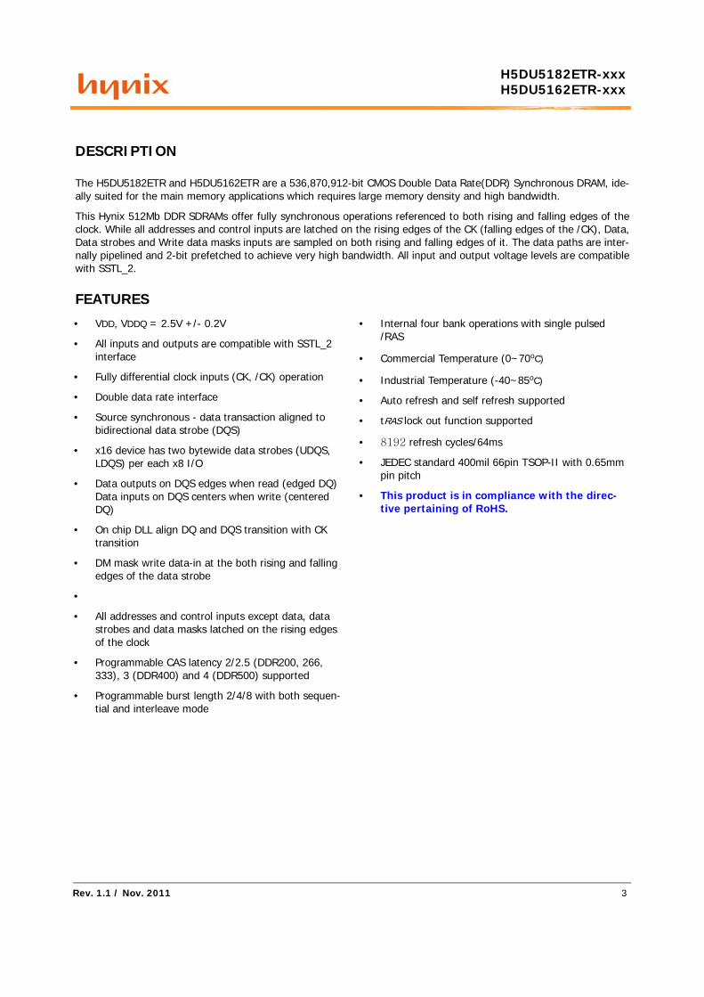
FUNCTIONAL BLOCK DIAGRAM (64Mx8)
4Banks x 16Mbit x 8 I/O Double Data Rate Synchronous DRAM
Sense AMP
Sense AMP
Sense AMP
ModeRegister
CommandDecoder
CLK/CLKCKE/CS/RAS/CAS/WEDM
BankControl
ModeRegister
RowDecoder
16Mx8 BANK 0
16Mx8 BANK 1
16Mx8 BANK 216Mx8 BANK 3
MemoryCell
Array
Sense AMP
ColumnDecoder
AddressBuffer
A0A1
AmaxBA0BA1
Column AddressCounter
8
Output Buffer
DQ0
DQ7
Input Buffer
DS
16
2-bit Prefetch Unit
Write Data Register2-bit Prefetch Unit 8
16
Data StrobeTransmitter
Data StrobeReceiver
DQS
DSDLLBlock
CLK,/CLK
CLK_DLL
ModeRegister
Rev. 1.1 / Nov. 2011 8
1H5DU5182ETR-xxxH5DU5162ETR-xxx
FUNCTIONAL BLOCK DIAGRAM (32Mx16)
4Banks x 8Mbit x 16 I/O Double Data Rate Synchronous DRAM
Sense AMP
Sense AMP
Sense AMP
ModeRegister
CommandDecoder
CLK/CLKCKE/CS/RAS/CAS/WE
UDQM
BankControl
ModeRegister
RowDecoder
8Mx16 BANK 0
8Mx16 BANK 1
8Mx16 BANK 28Mx16 BANK 3
MemoryCell
Array
Sense AMP
ColumnDecoder
AddressBuffer
A0A1
AmaxBA0BA1
Column AddressCounter
16
Output Buffer
DQ0
DQ15
Input Buffer
DS
32
2-bit Prefetch Unit
Write Data Register2-bit Prefetch Unit 16
32
Data StrobeTransmitter
Data StrobeReceiver
UDQS,LDQS
UDQS,LDQS
DLLBlock
CLK,/CLK
CLK_DLL
ModeRegister
LDQM
Rev. 1.1 / Nov. 2011 9
1H5DU5182ETR-xxxH5DU5162ETR-xxx
SIMPLIFIED COMMAND TRUTH TABLE
Command CKEn-1 CKEn CS RAS CAS WE ADDR A10/AP BA Note
Extended Mode Register Set H X L L L L OP code 1,2
Mode Register Set H X L L L L OP code 1,2
Device DeselectH X
H X X XX 1
No Operation L H H H
Bank Active H X L L H H RA V 1
ReadH X L H L H CA
LV
1
Read with Autoprecharge H 1,3
WriteH X L H L L CA
LV
1
Write with Autoprecharge H 1,4
Precharge All BanksH X L L H L X
H X 1,5
Precharge selected Bank L V 1
Read Burst Stop H X L H H L X 1
Auto Refresh H H L L L H X 1
Self Refresh
Entry H L L L L H
X
1
Exit L HH X X X
1L H H H
Precharge Power Down
Mode
Entry H LH X X X
X
1
L H H H 1
Exit L HH X X X 1
L H H H 1
Active Power Down Mode
Entry H LH X X X
X
1
L V V V 1
Exit L H X 1
( H=Logic High Level, L=Logic Low Level, X=Don’t Care, V=Valid Data Input, OP Code=Operand Code, NOP=No Operation )
Rev. 1.1 / Nov. 2011 10
1H5DU5182ETR-xxxH5DU5162ETR-xxx
WRITE MASK TRUTH TABLE
Function CKEn-1 CKEn /CS, /RAS, /CAS, /WE DM ADDR A10/
AP BA Note
Data Write H X X L X 1,2
Data-In Mask H X X H X 1,2
Note : 1. Write Mask command masks burst write data with reference to LDQS/UDQS(Data Strobes) and it is not related with read data.
In case of x16 data I/O, LDM and UDM control lower byte(DQ0~7) and Upper byte(DQ8~15) respectively.2. In here, Don’t Care means logical value only, it doesn’t mean ’Don’t care for DC level of each signals’. DC level should be out of
VIHmin ~ VILmax
Note : 1. UDM, LDM states are Don’t Care. Refer to below Write Mask Truth Table.(note 6)2. OP Code(Operand Code) consists of A0~A12 and BA0~BA1 used for Mode Register setting during Extended MRS or MRS. Before
entering Mode Register Set mode, all banks must be in a precharge state and MRS command can be issued after tRP period from Prechagre command.
3. If a Read with Auto-precharge command is detected by memory component in CK(n), then there will be no command presented to activate bank until CK(n+BL/2+tRP).
4. If a Write with Auto-precharge command is detected by memory component in CK(n), then there will be no command presented to activate bank until CK(n+BL/2+1+tDPL+tRP). Last Data-In to Prechage delay(tDPL) which is also called Write Recovery Time(tWR) is needed to guarantee that the last data have been completely written.
5. If A10/AP is High when Precharge command being issued, BA0/BA1 are ignored and all banks are selected to be precharged.6. In here, Don’t Care means logical value only, it doesn’t mean ’Don’t care for DC level of each signals’. DC level should be out of
VIHmin ~ VILmax
Rev. 1.1 / Nov. 2011 11
1H5DU5182ETR-xxxH5DU5162ETR-xxx
SIMPLIFIED STATE DIAGRAM
IDLE
BANKACTIVE
SELFREFRESH
ModeREGISTER
SET
IDLEPOWERDOWN ACTIVE
POWERDOWN
AUTOREFRESH
WRITE WITH
AUTOPRECHARGE
READ WITH
AUTOPRECHARGE
BANKACTIVE
POWER-UP
POWER APPLIED
WRITE READ
(E)MRS SREF
SREX
AREF
CLE HIGH
CKE LOW
ACTIVECLE HIGH
CKE LOW
Writ
e
READREADAP
WRITEAP
PRE(PALL)
WRITEAP
WRITEAP
WRITE
READ
PRE(PALL)PRE(PALL)
Command Input
Automatic Sequence
Rev. 1.1 / Nov. 2011 12
1H5DU5182ETR-xxxH5DU5162ETR-xxx
POWER-UP SEQUENCE AND DEVICE INITIALIZATION
DDR SDRAMs must be powered up and initialized in a predefined manner. Operational procedures other than thosespecified may result in undefined operation. Power must first be applied to VDD, then to VDDQ, and finally to VREF(and to the system VTT). VTT must be applied after VDDQ to avoid device latch-up, which may cause permanent dam-age to the device. VREF can be applied anytime after VDDQ, but is expected to be nominally coincident with VTT.Except for CKE, inputs are not recognized as valid until after VREF is applied. CKE is an SSTL_2 input, but will detect anLVCMOS LOW level after VDD is applied. Maintaining an LVCMOS LOW level on CKE during power-up is required toguarantee that the DQ and DQS outputs will be in the High-Z state, where they will remain until driven in normal oper-ation (by a read access). After all power supply and reference voltages are stable, and the clock is stable, the DDRSDRAM requires a 200us delay prior to applying an executable command.
Once the 200us delay has been satisfied, a DESELECT or NOP command should be applied, and CKE should bebrought HIGH. Following the NOP command, a PRECHARGE ALL command should be applied. Next a EXTENDEDMODE REGISTER SET command should be issued for the Extended Mode Register, to enable the DLL, then a MODEREGISTER SET command should be issued for the Mode Register, to reset the DLL, and to program the operatingparameters. After the DLL reset, tXSRD(DLL locking time) should be satisfied for read command. After the Mode Reg-ister set command, a PRECHARGE ALL command should be applied, placing the device in the all banks idle state.
Once in the idle state, two AUTO REFRESH cycles must be performed. Additionally, a MODE REGISTER SET commandfor the Mode Register, with the reset DLL bit deactivated low (i.e. to program operating parameters without resettingthe DLL) must be performed. Following these cycles, the DDR SDRAM is ready for normal operation.
1. Apply power - VDD, VDDQ, VTT, VREF in the following power up sequencing and attempt to maintain CKE at LVC-MOS low state. (All the other input pins may be undefined.)
• VDD and VDDQ are driven from a single power converter output.
• VTT is limited to 1.44V (reflecting VDDQ(max)/2 + 50mV VREF variation + 40mV VTT variation.
• VREF tracks VDDQ/2.
• A minimum resistance of 42 Ohms (22 ohm series resistor + 22 ohm parallel resistor - 5% tolerance) limits the input current from the VTT supply into any pin.
• If the above criteria cannot be met by the system design, then the following sequencing and voltage relation-ship must be adhered to during power up.
2. Start clock and maintain stable clock for a minimum of 200usec.
3. After stable power and clock, apply NOP condition and take CKE high.
4. Issue Extended Mode Register Set (EMRS) to enable DLL.
5. Issue Mode Register Set (MRS) to reset DLL and set device to idle state with bit A8=high. (An additional 200 cycles(tXSRD) of clock are required for locking DLL)
6. Issue Precharge commands for all banks of the device.
7. Issue 2 or more Auto Refresh commands.
8. Issue a Mode Register Set command to initialize the mode register with bit A8 = Low
Voltage description Sequencing Voltage relationship to avoid latch-up
VDDQ After or with VDD < VDD + 0.3V
VTT After or with VDDQ < VDDQ + 0.3V
VREF After or with VDDQ < VDDQ + 0.3V
Rev. 1.1 / Nov. 2011 13
1H5DU5182ETR-xxxH5DU5162ETR-xxx
Power-Up Sequence
CODECODE CODE CODECODE
CODECODE CODE CODECODE
CODE CODECODECODECODE
NOP PRE MRSEMRS PRENOP MRSAREF ACT RD
VDD
VDDQ
VTT
VREF
/CLKCLK
CKE
CMD
DM
ADDR
A10
BA0, BA1
DQS
DQ'S
LVCMOS Low Level
tIS tIH
tVTD
T=200usec tRP tMRD tRP tRFC tMRD
tXSRD*
READNon-ReadCommand
Power UPVDD and CK stable Precharge All
EMRS Set MRS SetReset DLL
(with A8=H)
Precharge All 2 or moreAuto Refresh
MRS Set(with A8=L)
* 200 cycle(tXSRD) of CK are required (for DLL locking) before Read Command
tMRD
Rev. 1.1 / Nov. 2011 14
1H5DU5182ETR-xxxH5DU5162ETR-xxx
MODE REGISTER SET (MRS)
The mode register is used to store the various operating modes such as /CAS latency, addressing mode, burst length, burst type, test mode, DLL reset. The mode register is programed via MRS command. This command is issued by the low signals of /RAS, /CAS, /CS, /WE and BA0. This command can be issued only when all banks are in idle state and CKE must be high at least one cycle before the Mode Register Set Command can be issued. Two cycles are required to write the data in mode register. During the MRS cycle, any command cannot be issued. Once mode register field is determined, the information will be held until reset by another MRS command.
BA1 BA0 A12 A11 A10 A9 A8 A7 A6 A5 A4 A3 A2 A1 A0
0 0 Operating Mode CAS Latency BT Burst Length
BA0 MRS Type
0 MRS
1 EMRS
A12~A9 A8 A7 A6~A0 Operating Mode
0 0 0 Valid Normal Operation
0 1 0 Valid Normal Operation/ Reset DLL
0 0 1 VS Vendor specific Test Mode
- - - - All other states reserved
A6 A5 A4 CAS Latency
0 0 0 Reserved
0 0 1 Reserved
0 1 0 2
0 1 1 3
1 0 0 4
1 0 1 1.5
1 1 0 2.5
1 1 1 Reserved
A3 Burst Type
0 Sequential
1 Interleave
A2 A1 A0Burst Length
Sequential Interleave
0 0 0 Reserved Reserved
0 0 1 2 2
0 1 0 4 4
0 1 1 8 8
1 0 0 Reserved Reserved
1 0 1 Reserved Reserved
1 1 0 Reserved Reserved
1 1 1 Reserved Reserved
Rev. 1.1 / Nov. 2011 15
1H5DU5182ETR-xxxH5DU5162ETR-xxx
BURST DEFINITION
BURST LENGTH & TYPE
Read and write accesses to the DDR SDRAM are burst oriented, with the burst length being programmable. The burstlength determines the maximum number of column locations that can be accessed for a given Read or Write com-mand. Burst lengths of 2, 4 or 8 locations are available for both the sequential and the interleaved burst types.Reserved states should not be used, as unknown operation or incompatibility with future versions may result.
When a Read or Write command is issued, a block of columns equal to the burst length is effectively selected. Allaccesses for that burst take place within this block, meaning that the burst wraps within the block if a boundary isreached. The block is uniquely selected by A1-Ai when the burst length is set to two, by A2 -Ai when the burst lengthis set to four and by A3 -Ai when the burst length is set to eight (where Ai is the most significant column address bitfor a given configuration). The remaining (least significant) address bit(s) is (are) used to select the starting locationwithin the block. The programmed burst length applies to both Read and Write bursts.
Accesses within a given burst may be programmed to be either sequential or interleaved; this is referred to as theburst type and is selected via bit A3. The ordering of accesses within a burst is determined by the burst length, theburst type and the starting column address, as shown in Burst Definition Table
Burst Length Starting Address (A2,A1,A0)
Sequential Interleave
2XX0 0, 1 0, 1
XX1 1, 0 1, 0
4
X00 0, 1, 2, 3 0, 1, 2, 3
X01 1, 2, 3, 0 1, 0, 3, 2
X10 2, 3, 0, 1 2, 3, 0, 1
X11 3, 0, 1, 2 3, 2, 1, 0
8
000 0, 1, 2, 3, 4, 5, 6, 7 0, 1, 2, 3, 4, 5, 6, 7
001 1, 2, 3, 4, 5, 6, 7, 0 1, 0, 3, 2, 5, 4, 7, 6
010 2, 3, 4, 5, 6, 7, 0, 1 2, 3, 0, 1, 6, 7, 4, 5
011 3, 4, 5, 6, 7, 0, 1, 2 3, 2, 1, 0, 7, 6, 5, 4
100 4, 5, 6, 7, 0, 1, 2, 3 4, 5, 6, 7, 0, 1, 2, 3
101 5, 6, 7, 0, 1, 2, 3, 4 5, 4, 7, 6, 1, 0, 3, 2
110 6, 7, 0, 1, 2, 3, 4, 5 6, 7, 4, 5, 2, 3, 0, 1
111 7, 0, 1, 2, 3, 4, 5, 6 7, 6, 5, 4, 3, 2, 1, 0
Rev. 1.1 / Nov. 2011 16
1H5DU5182ETR-xxxH5DU5162ETR-xxx
CAS LATENCY
The Read latency or CAS latency is the delay in clock cycles between the registration of a Read command and theavailability of the first burst of output data. The latency can be programmed 2 or 2.5 clocks for DDR266/333 or 3clocks for DDR400 product.
If a Read command is registered at clock edge n, and the latency is m clocks, the data is available nominally coincidentwith clock edge n + m.
Reserved states should not be used as unknown operation or incompatibility with future versions may result.
DLL RESET
The DLL must be enabled for normal operation. DLL enable is required during power up initialization, and upon return-ing to normal operation after having disabled the DLL for the purpose of debug or evaluation. The DLL is automaticallydisabled when entering self refresh operation and is automatically re-enabled upon exit of self refresh operation. Anytime the DLL is enabled, 200 clock cycles must occur to allow time for the internal clock to lock to the externallyapplied clock before an any command can be issued.
OUTPUT DRIVER IMPEDANCE CONTROL
The normal drive strength for all outputs is specified to be SSTL_2, Class II. Hynix also supports a half strength driveroption, intended for lighter load and/or point-to-point environments. Selection of the half strength driver option willreduce the output drive strength by 50% of that of the full strength driver. I-V curves for both the full strength driverand the half strength driver are included in this document.
Rev. 1.1 / Nov. 2011 17
1H5DU5182ETR-xxxH5DU5162ETR-xxx
EXTENDED MODE REGISTER SET (EMRS)
The Extended Mode Register controls functions beyond those controlled by the Mode Register; these additional func-tions include DLL enable/disable, output driver strength selection(optional). These functions are controlled via the bits shown below. The Extended Mode Register is programmed via the Mode Register Set command (BA0=1 and BA1=0) and will retain the stored information until it is programmed again or the device loses power.
The Extended Mode Register must be loaded when all banks are idle and no bursts are in progress, and the controller must wait the specified time before initiating any subsequent operation. Violating either of these requirements will result in unspecified operation.
BA1 BA0 A12 A11 A10 A9 A8 A7 A6 A5 A4 A3 A2 A1 A0
0 1 Operating Mode 0* DS DLL
BA0 MRS Type
0 MRS
1 EMRS
An~A3 A2~A0 Operating Mode
0 Valid Normal Operation
_ _ All other states reserved
A0 DLL enable
0 Enable
1 Disable
A1 Output Driver Impedance Control
0 Full Strength Driver
1 Half Strength Driver
* This part do not support/QFC function, A2 must be programmed to Zero.
Rev. 1.1 / Nov. 2011 18
1H5DU5182ETR-xxxH5DU5162ETR-xxx
ABSOLUTE MAXIMUM RATINGS
Note: Operation at above absolute maximum rating can adversely affect device reliability
DC OPERATING CONDITIONS (TA=-40 to 85 oC, Voltage referenced to VSS = 0V)
Note: 1. VDDQ must not exceed the level of VDD.2. VIL (min) is acceptable -1.5V AC pulse width with < 5ns of duration. 3. VREF is expected to be equal to 0.5*VDDQ of the transmitting device, and to track variations in the dc level of the same. Peak to peak noise on VREF may not exceed ±2% of the DC value.4. VID is the magnitude of the difference between the input level on CK and the input level on /CK.
Parameter Symbol Rating Unit
Operating Temperature (Ambient) TA0 ~ 70(Commertial Part) oC
-40 ~ 85(Industrial Part) oC
Storage Temperature TSTG -55 ~ 150 oCVoltage on VDD relative to VSS VDD -1.0 ~ 3.6 VVoltage on VDDQ relative to VSS VDDQ -1.0 ~ 3.6 VVoltage on inputs relative to VSS VINPUT -1.0 ~ 3.6 VVoltage on I/O pins relative to VSS VIO -0.5 ~3.6 VOutput Short Circuit Current IOS 50 mA
Soldering Temperature Time TSOLDER 260 10 oC Sec
Parameter Symbol Min Typ. Max Unit
Power Supply Voltage VDD 2.3 2.5 2.7 V
Power Supply Voltage 1 VDDQ 2.3 2.5 2.7 V
Input High Voltage VIH VREF + 0.15 - VDDQ + 0.3 V
Input Low Voltage2 VIL -0.3 - VREF - 0.15 V
Termination Voltage VTT VREF - 0.04 VREF VREF + 0.04 V
Reference Voltage3 VREF 0.49*VDDQ 0.5*VDDQ 0.51*VDDQ V
Input Voltage Level, CK and CK inputs VIN(DC) -0.3 - VDDQ+0.3 V
Input Differential Voltage, CK and CK inputs4 VID(DC) 0.36 - VDDQ+0.6 V
V-I Matching: Pullup to Pulldown Current Ratio5 VI(RATIO) 0.71 - 1.4 -
Input Leakage Current6 ILI -2 - 2 uA
Output Leakage Current7 ILO -5 - 5 uA
Normal Strength Output Driver(VOUT=VTT±0.84)
Output High Current(min VDDQ, min VREF, min VTT)
IOH -16.8 - - mA
Output Low Current(min VDDQ, max VREF, max VTT)
IOL 16.8 - - mA
Half Strength Output Driver(VOUT=VTT±0.68)
Output High Current(min VDDQ, min VREF, min VTT)
IOH -13.6 - - mA
Output Low Current(min VDDQ, max VREF, max VTT)
IOL 13.6 - - mA
Rev. 1.1 / Nov. 2011 19
1H5DU5182ETR-xxxH5DU5162ETR-xxx
5. The ratio of the pullup current to the pulldown current is specified for the same temperature and voltage, over the entire temper-ature and voltage range, for device drain to source voltages from 0.25V to 1.0V. For a given output, it represents the maximum dif-ference between pullup and pulldown drivers due to process variation. The full variation in the ratio of the maximum to minimumpullup and pulldown current will not exceed 1/7 for device drain to source voltages from 0.1 to 1.0.
6. VIN=0 to VDD, All other pins are not tested under VIN =0V.7. DQs are disabled, VOUT=0 to VDDQ
IDD SPECIFICATION AND CONDITIONS (TA=-40 to 85 oC, Voltage referenced to VSS = 0V)
Test Conditions
Test Condition SymbolOperating Current:One bank; Active - Precharge; tRC=tRC(min); tCK=tCK(min); DQ,DM and DQS inputs changing twice per clock cycle; address and control inputs changing once per clock cycle
IDD0
Operating Current:One bank; Active - Read - Precharge; Burst Length=2; tRC=tRC(min); tCK=tCK(min); address and control inputs changing once per clock cycle
IDD1
Precharge Power Down Standby Current:All banks idle; Power down mode; CKE=Low, tCK=tCK(min) IDD2P
Idle Standby Current:/CS=High, All banks idle; tCK=tCK(min); CKE=High; address and control inputs changing once per clock cycle. VIN=VREF for DQ, DQS and DM
IDD2F
Idle Quiet Standby Current:/CS>=Vih(min); All banks idle; CKE>=Vih(min); Addresses and other control inputs stable, Vin=Vref for DQ, DQS and DM
IDD2Q
Active Power Down Standby Current:One bank active; Power down mode; CKE=Low, tCK=tCK(min) IDD3P
Active Standby Current:/CS=HIGH; CKE=HIGH; One bank; Active-Precharge; tRC=tRAS(max); tCK=tCK(min); DQ, DM and DQS inputs changing twice per clock cycle; Address and other control inputs changing once per clock cycle
IDD3N
Operating Current:Burst=2; Reads; Continuous burst; One bank active; Address and control inputs changing once per clock cycle; tCK=tCK(min); IOUT=0mA
IDD4R
Operating Current:Burst=2; Writes; Continuous burst; One bank active; Address and control inputs changing once per clock cycle; tCK=tCK(min); DQ, DM and DQS inputs changing twice per clock cycle
IDD4W
Auto Refresh Current:tRC=tRFC(min) - 8*tCK for DDR200 at 100Mhz, 10*tCK for DDR266A & DDR266B at 133Mhz; distributed refreshtRC=tRFC(min) - 14*tCK for DDR400 at 200Mhz
Operating Current - Four Bank Operation:Four bank interleaving with BL=4, Refer to the following page for detailed test condition IDD7
Rev. 1.1 / Nov. 2011 20
1H5DU5182ETR-xxxH5DU5162ETR-xxx
DETAILED TEST CONDITIONS FOR DDR SDRAM IDD1 & IDD7IDD1: Operating current: One bank operation
1. Typical Case: VDD = 2.5V, T=25 oC for DDR200, 266, 333; VDD = 2.6V, T=25 oC for DDR400
2. Worst Case: VDD = 2.7V, T= 0 oC
3. Only one bank is accessed with tRC(min), Burst Mode, Address and Control inputs on NOP edge are changing once per clock cycle. lout = 0mA
4. Timing patterns
- DDR200(100Mhz, CL=2): tCK = 10ns, CL2, BL=2, tRCD = 2*tCK, tRC = 10*tCK, tRAS = 5*tCK Read: A0 N R0 N N P0 N A0 N - repeat the same timing with random address changing 50% of data changing at every burst
- DDR266B(133Mhz, CL=2.5): tCK = 7.5ns, CL=2.5, BL=4, tRCD = 3*tCK, tRC = 9*tCK, tRAS = 5*tCK Read: A0 N N R0 N P0 N N N A0 N - repeat the same timing with random address changing 50% of data changing at every burst
- DDR266A (133Mhz, CL=2): tCK = 7.5ns, CL=2, BL=4, tRCD = 3*tCK, tRC = 9*tCK, tRAS = 5*tCK Read: A0 N N R0 N P0 N N N A0 N - repeat the same timing with random address changing 50% of data changing at every burst
- DDR333(166Mhz, CL=2.5): tCK = 6ns, CL=2, BL=4, tRCD = 3*tCK, tRC = 10*tCK, tRAS = 7*tCK Read: A0 N N R0 N N N P0 N N A0 N - repeat the same timing with random address changing 50% of data changing at every burst
- DDR400(200Mhz, CL=3): tCK = 5ns, CL=3, BL=4, tRCD = 3*tCK, tRC = 11*tCK, tRAS = 8*tCK Read: A0 N N R0 N N N N P0 N N - repeat the same timing with random address changing 50% of data changing at every burst
1. Typical Case: VDD = 2.5V, T=25 oC for DDR200, 266, 333; VDD = 2.6V, T=25 oC for DDR400
2. Worst Case: VDD = 2.7V, T= 0 oC
3. Four banks are being interleaved with tRC(min), Burst Mode, Address and Control inputs on NOP edge are not changing. lout = 0mA
4. Timing patterns
- DDR200(100Mhz, CL=2): tCK = 10ns, CL2, BL=4, tRRD = 2*tCK, tRCD= 3*tCK, Read with Autoprecharge Read: A0 N A1 R0 A2 R1 A3 R2 A0 R3 A1 R0 - repeat the same timing with random address changing 50% of data changing at every burst
- DDR266B(133Mhz, CL=2.5): tCK = 7.5ns, CL=2.5, BL=4, tRRD = 2*tCK, tRCD = 3*tCK Read with autoprecharge Read: A0 N A1 R0 A2 R1 A3 R2 N R3 A0 N A1 R0 - repeat the same timing with random address changing 50% of data changing at every burst
- DDR266A (133Mhz, CL=2): tCK = 7.5ns, CL2=2, BL=4, tRRD = 2*tCK, tRCD = 3*tCK Read: A0 N A1 R0 A2 R1 A3 R2 N R3 A0 N A1 R0 - repeat the same timing with random address changing 50% of data changing at every burst
- DDR333(166Mhz, CL=2.5): tCK = 6ns, CL=2.5, BL=4, tRRD = 2*tCK, tRCD = 3*tCK, Read with autoprecharge Read: A0 N A1 R0 A2 R1 A3 R2 N R3 A0 N A1 R0 - repeat the same timing with random address changing 50% of data changing at every burst
- DDR400(200Mhz, CL=3): tCK = 5ns, CL = 2, BL = 4, tRRD = 2*tCK, tRCD = 3*tCK, Read with autoprecharge Read: A0 N A1 R0 A2 R1 A3 R2 N R3 A0 N A1 R0 - repeat the same timing with random address changing 50% of data changing at every burst
Operating Current IDD0 90 80 65 65 65 mAOperating Current IDD1 100 90 80 80 80 mAPrecharge Power Down Standby Current IDD2P 5 5 5 5 5 mA
Idle Standby Current IDD2F 23 23 23 23 23 mAIdle Quiet Standby Current IDD2Q 20 20 20 20 20 mAActive Power Down Standby Current IDD3P 20 20 15 15 15 mAActive Standby Current IDD3N 40 40 40 40 40 mAOperating Current IDD4R 150 135 95 95 95
mAOperating Current IDD4W 160 135 110 110 110
Auto Refresh Current IDD5 160 135 100 100 100
Self Refresh CurrentNormal
IDD65 5 5 5 5 mA
Low Power 3 3 3 3 3 mAOperating Current - Four Bank Operation IDD7 310 260 240 240 240 mA
Parameter SymbolSpeed
UnitDDR500 DDR400B DDR333 DDR266A DDR266B
Operating Current IDD0 90 80 65 65 65 mAOperating Current IDD1 100 90 80 80 80 mAPrecharge Power Down Standby Current IDD2P 5 5 5 5 5 mA
Idle Standby Current IDD2F 23 23 23 23 23 mAIdle Quiet Standby Current IDD2Q 20 20 20 20 20 mAActive Power Down Standby Current IDD3P 20 20 15 15 15 mAActive Standby Current IDD3N 40 40 40 40 40 mAOperating Current IDD4R 150 135 95 95 95
mAOperating Current IDD4W 160 135 110 110 110
Auto Refresh Current IDD5 160 135 100 100 100
Self Refresh CurrentNormal
IDD65 5 5 5 5 mA
Low Power 3 3 3 3 3 mAOperating Current - Four Bank Operation IDD7 310 260 240 240 240 mA
Rev. 1.1 / Nov. 2011 22
1H5DU5182ETR-xxxH5DU5162ETR-xxx
AC OPERATING CONDITIONS (TA=-40 to 85 oC, Voltage referenced to VSS = 0V)
Note: 1. VID is the magnitude of the difference between the input level on CK and the input on /CK.2. The value of VIX is expected to equal 0.5*VDDQ of the transmitting device and must track variations in the DC level of the same.
*For more information about AC Overshoot/Undershoot Specifications, refer to “Device Operation” section in hynix website.
AC OPERATING TEST CONDITIONS (TA=-40 to 85oC, Voltage referenced to VSS = 0V)
Parameter Symbol Min Max Unit
Input High (Logic 1) Voltage, DQ, DQS and DM signals VIH(AC) VREF + 0.31 - V
Input Low (Logic 0) Voltage, DQ, DQS and DM signals VIL(AC) - VREF - 0.31 V
Input Differential Voltage, CK and /CK inputs1 VID(AC) 0.7 VDDQ + 0.6 V
Input Crossing Point Voltage, CK and /CK inputs2 VIX(AC) 0.5*VDDQ-0.2 0.5*VDDQ+0.2 V
Parameter Value Unit
Reference Voltage VDDQ x 0.5 V
Termination Voltage VDDQ x 0.5 V
AC Input High Level Voltage (VIH, min) VREF + 0.31 V
AC Input Low Level Voltage (VIL, max) VREF - 0.31 V
Input Timing Measurement Reference Level Voltage VREF V
Output Timing Measurement Reference Level Voltage VTT V
Input Signal maximum peak swing 1.5 V
Input minimum Signal Slew Rate 1 V/ns
Termination Resistor (RT) 50 Ω
Series Resistor (RS) 25 W
Output Load Capacitance for Access Time Measurement (CL) 30 pF
Rev. 1.1 / Nov. 2011 23
1H5DU5182ETR-xxxH5DU5162ETR-xxx
AC CHARACTERISTICS (note: 1 - 9 / AC operating conditions unless otherwise noted)
Average Periodic Refresh Interval13,25 tREFI - 7.8 - 7.8 - 7.8 - 7.8 - 7.8 us
Rev. 1.1 / Nov. 2011 25
1H5DU5182ETR-xxxH5DU5162ETR-xxx
Note:1. All voltages referenced to Vss.2. Tests for ac timing, IDD, and electrical, ac and dc characteristics, may be conducted at nominal reference/supply voltage levels,
but the related specifications and device operation are guaranteed for the full voltage range specified.3. Below figure represents the timing reference load used in defining the relevant timing parameters of the part. It is not intended to
be either a precise representation of the typical system environment nor a depiction of the actual load presented by a production tester. System designers will use IBIS or other simulation tools to correlate the timing reference load to a system environment. Manufacturers will correlate to their production test conditions (generally a coaxial transmission line terminated at the tester elec-tronics).
4. AC timing and IDD tests may use a VIL to VIHswing of up to 1.5 V in the test environment, but input timing is still referenced to
VREF (or to the crossing point for CK, /CK), and parameter specifications are guaranteed for the specified ac input levels under
normal use conditions. The minimum slew rate for the input signals is 1 V/ns in the range between VIL(ac) and VIH(ac).
5. The ac and dc input level specifications are as defined in the SSTL_2 Standard (i.e., the receiver will effectively switch as a result
of the signal crossing the ac input level and will remain in that state as long as the signal does not ring back above (below) the
dc input LOW (HIGH) level.
6. Inputs are not recognized as valid until VREF stabilizes. Exception: during the period before VREF stabilizes, CKE < 0.2VDDQ is
recognized as LOW.
7. The CK, /CK input reference level (for timing referenced to CK, /CK) is the point at which CK and /CK cross; the input reference
level for signals other than CK, /CK is VREF.
8. The output timing reference voltage level is VTT.
9. Operation or timing that is not specified is illegal and after such an event, in order to guarantee proper operation, the DRAM must be powered down and then restarted through the specified initialization sequence before normal operation can continue.
10. tHZ and tLZ transitions occur in the same access time windows as valid data transitions. These parameters are not referenced to
a specific voltage level but specify when the device output is no longer driving (HZ), or begins driving (LZ).
11. The maximum limit for this parameter is not a device limit. The device will operate with a greater value for this parameter, but system performance (bus turnaround) will degrade accordingly.
12. The specific requirement is that DQS be valid (HIGH, LOW, or at some point on a valid transition) on or before this CK edge. A
valid transition is defined as monotonic and meeting the input slew rate specifications of the device. When no writes were previ-
ously in progress on the bus, DQS will be transitioning from High-Z to logic LOW. If a previous write was in progress, DQS could
be HIGH, LOW, or transitioning from HIGH to LOW at this time, depending on tDQSS.
13. A maximum of eight AUTO REFRESH commands can be posted to any given DDR SDRAM device.
14. For command/address input slew rate ≥ 1.0 V/ns.
15. For command/address input slew rate ≥ 0.5 V/ns and < 1.0 V/ns
16. For CK & /CK slew rate ≥ 1.0 V/ns (single-ended)
17. These parameters guarantee device timing, but they are not necessarily tested on each device.
They may be guaranteed by device design or tester correlation.
18. Slew Rate is measured between VOH(ac) and VOL(ac).
19. Min (tCL, tCH) refers to the smaller of the actual clock low time and the actual clock high time as provided to the device (i.e. this
value can be greater than the minimum specification limits for tCL and tCH).
For example, tCL and tCH are = 50% of the period, less the half period jitter (tJIT(HP)) of the clock source, and less the half period jitter due to crosstalk (tJIT(crosstalk)) into the clock traces.
Figure: Timing Reference Load
VDDQ
50Output(VOUT)
30 pF
Ω
Rev. 1.1 / Nov. 2011 26
1H5DU5182ETR-xxxH5DU5162ETR-xxx
20.tQH = tHP - tQHS, where:
tHP = minimum half clock period for any given cycle and is defined by clock high or clock low (tCH, tCL). tQHS accounts for 1) The
pulse duration distortion of on-chip clock circuits; and 2) The worst case push--out of DQS on one transition followed by the
worst case pull--in of DQ on the next transition, both of which are, separately, due to data pin skew and output pattern effects,
and p-channel to n-channel variation of the output drivers.
21. tDQSQ:
Consists of data pin skew and output pattern effects, and p-channel to n-channel variation of the output drivers for any given
cycle.
22. tDAL = (tWR/tCK) + (tRP/tCK)
For each of the terms above, if not already an integer, round to the next highest integer.
23. In all circumstances, tXSNR can be satisfied using
tXSNR = tRFCmin + 1*tCK
24. The only time that the clock frequency is allowed to change is during self-refresh mode.
25. If refresh timing or tDS/tDH is violated, data corruption may occur and the data must be re-written with valid data before a valid
READ can be executed.
Rev. 1.1 / Nov. 2011 27
1H5DU5182ETR-xxxH5DU5162ETR-xxx
SYSTEM CHARACTERISTICS CONDITIONS for DDR SDRAMSThe following tables are described specification parameters that required in systems using DDR devices to ensure proper performannce. These characteristics are for system simulation purposes and are guaranteed by design.Input Slew Rate for DQ/DM/DQS (Table a.)
Address & Control Input Setup & Hold Time Derating (Table b.)
DQ & DM Input Setup & Hold Time Derating (Table c.)
DQ & DM Input Setup & Hold Time Derating for Rise/Fall Delta Slew Rate (Table d.)
Output Slew Rate Characteristics (for x8 Devices) (Table e.)
Output Slew Rate Matching Ratio (Pullup to Pulldown)
- - - - 0.71 1.4 5,12
Rev. 1.1 / Nov. 2011 28
1H5DU5182ETR-xxxH5DU5162ETR-xxx
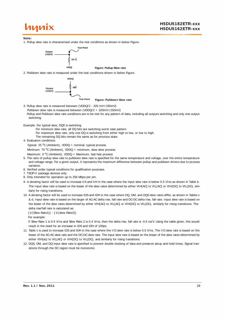
Note:1. Pullup slew rate is characterized under the test conditions as shown in below Figure.
2. Pulldown slew rate is measured under the test conditions shown in below Figure.
3. Pullup slew rate is measured between (VDDQ/2 - 320 mV±250mV) Pulldown slew rate is measured between (VDDQ/2 + 320mV±250mV) Pullup and Pulldown slew rate conditions are to be met for any pattern of data, including all outputs switching and only one output
switching.
Example: For typical slew, DQ0 is switching For minimum slew rate, all DQ bits are switching worst case pattern For maximum slew rate, only one DQ is switching from either high to low, or low to high. The remaining DQ bits remain the same as for previous state.4. Evaluation conditions Typical: 25 oC (Ambient), VDDQ = nominal, typical process Minimum: 70 oC (Ambient), VDDQ = minimum, slow-slow process Maximum: 0 oC (Ambient), VDDQ = Maximum, fast-fast process5. The ratio of pullup slew rate to pulldown slew rate is specified for the same temperature and voltage, over the entire temperature
and voltage range. For a given output, it represents the maximum difference between pullup and pulldown drivers due to process variation.
6. Verified under typical conditions for qualification purposes.7. TSOP-II package devices only.8. Only intended for operation up to 256 Mbps per pin.
9. A derating factor will be used to increase tIS and tIH in the case where the input slew rate is below 0.5 V/ns as shown in Table b. The Input slew rate is based on the lesser of the slew rates determined by either VIH(AC) to VIL(AC) or VIH(DC) to VIL(DC), sim-ilarly for rising transitions.
10. A derating factor will be used to increase tDS and tDH in the case where DQ, DM, and DQS slew rates differ, as shown in Tables c & d. Input slew rate is based on the larger of AC-AC delta rise, fall rate and DC-DC delta rise, fall rate. Input slew rate is based on the lesser of the slew rates determined by either VIH(AC) to VIL(AC) or VIH(DC) to VIL(DC), similarly for rising transitions. The delta rise/fall rate is calculated as:
{1/(Slew Rate1)} - {1/(slew Rate2)} For example: If Slew Rate 1 is 0.5 V/ns and Slew Rate 2 is 0.4 V/ns, then the delta rise, fall rate is -0.5 ns/V. Using the table given, this would
result in the need for an increase in tDS and tDH of 100ps.11. Table c is used to increase tDS and tDH in the case where the I/O slew rate is below 0.5 V/ns. The I/O slew rate is based on the
lesser of the AC-AC slew rate and the DC-DC slew rate. The input slew rate is based on the lesser of the slew rates determined by either VIH(ac) to VIL(AC) or VIH(DC) to VIL(DC), and similarly for rising transitions.
12. DQS, DM, and DQ input slew rate is specified to prevent double clocking of data and preserve setup and hold times. Signal tran-sitions through the DC region must be monotonic.
50
Output(VOUT)
VSSQ
Test Point
Figure: Pullup Slew rate
Ω
VDDQ
50
Test Point
Output(VOUT)
Figure: Pulldown Slew rate
Ω
Rev. 1.1 / Nov. 2011 29
1H5DU5182ETR-xxxH5DU5162ETR-xxx
CAPACITANCE (TA=25oC, f=100MHz)
Note: 1. VDD = min. to max., VDDQ = 2.3V to 2.7V, VODC = VDDQ/2, VOpeak-to-peak = 0.2V2. Pins not under test are tied to GND.3. These values are guaranteed by design and are tested on a sample basis only.