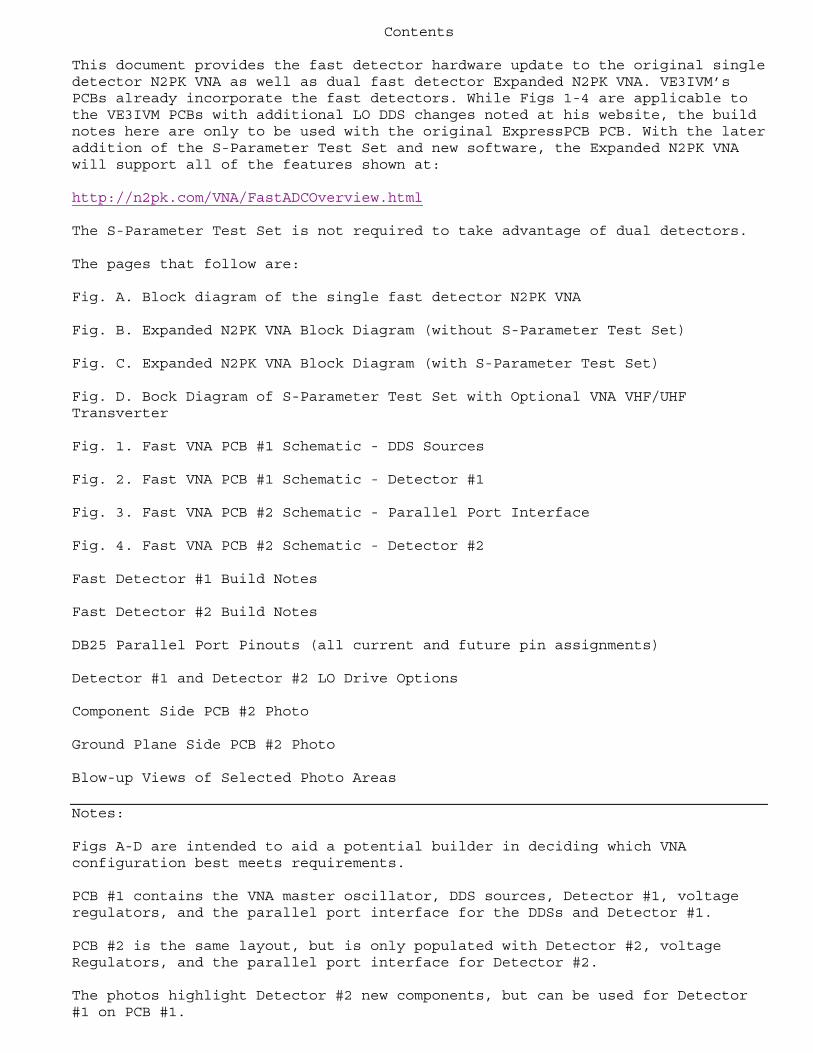
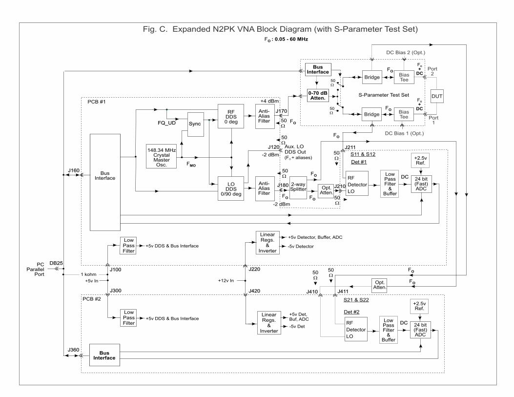
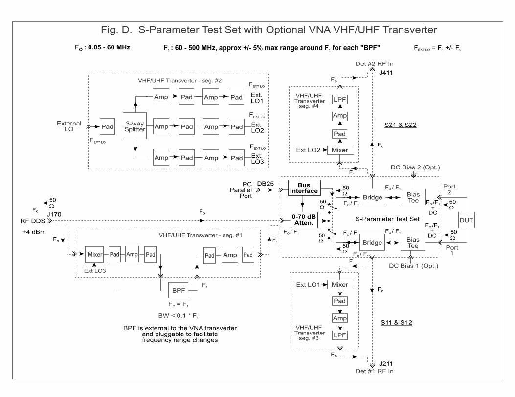
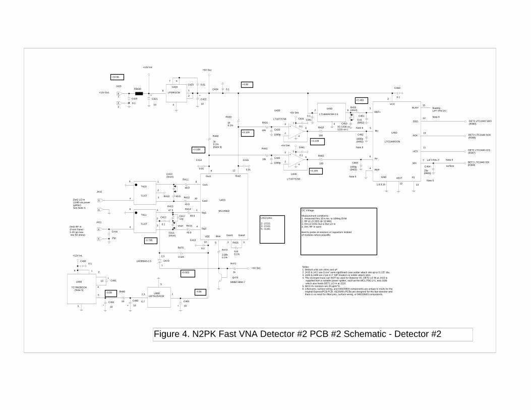
Contents This document provides the fast detector hardware update to the original single detector N2PK VNA as well as dual fast detector Expanded N2PK VNA. VE3IVM’s PCBs already incorporate the fast detectors. While Figs 1-4 are applicable to the VE3IVM PCBs with additional LO DDS changes noted at his website, the build notes here are only to be used with the original ExpressPCB PCB. With the later addition of the S-Parameter Test Set and new software, the Expanded N2PK VNA will support all of the features shown at: http://n2pk.com/VNA/FastADCOverview.html The S-Parameter Test Set is not required to take advantage of dual detectors. The pages that follow are: Fig. A. Block diagram of the single fast detector N2PK VNA Fig. B. Expanded N2PK VNA Block Diagram (without S-Parameter Test Set) Fig. C. Expanded N2PK VNA Block Diagram (with S-Parameter Test Set) Fig. D. Bock Diagram of S-Parameter Test Set with Optional VNA VHF/UHF Transverter Fig. 1. Fast VNA PCB #1 Schematic - DDS Sources Fig. 2. Fast VNA PCB #1 Schematic - Detector #1 Fig. 3. Fast VNA PCB #2 Schematic - Parallel Port Interface Fig. 4. Fast VNA PCB #2 Schematic - Detector #2 Fast Detector #1 Build Notes Fast Detector #2 Build Notes DB25 Parallel Port Pinouts (all current and future pin assignments) Detector #1 and Detector #2 LO Drive Options Component Side PCB #2 Photo Ground Plane Side PCB #2 Photo Blow-up Views of Selected Photo Areas Notes: Figs A-D are intended to aid a potential builder in deciding which VNA configuration best meets requirements. PCB #1 contains the VNA master oscillator, DDS sources, Detector #1, voltage regulators, and the parallel port interface for the DDSs and Detector #1. PCB #2 is the same layout, but is only populated with Detector #2, voltage Regulators, and the parallel port interface for Detector #2. The photos highlight Detector #2 new components, but can be used for Detector #1 on PCB #1.
Transcript
Contents This document provides the fast detector hardware update to the original single detector N2PK VNA as well as dual fast detector Expanded N2PK VNA. VE3IVM’s PCBs already incorporate the fast detectors. While Figs 1-4 are applicable to the VE3IVM PCBs with additional LO DDS changes noted at his website, the build notes here are only to be used with the original ExpressPCB PCB. With the later addition of the S-Parameter Test Set and new software, the Expanded N2PK VNA will support all of the features shown at: http://n2pk.com/VNA/FastADCOverview.html The S-Parameter Test Set is not required to take advantage of dual detectors. The pages that follow are: Fig. A. Block diagram of the single fast detector N2PK VNA Fig. B. Expanded N2PK VNA Block Diagram (without S-Parameter Test Set) Fig. C. Expanded N2PK VNA Block Diagram (with S-Parameter Test Set) Fig. D. Bock Diagram of S-Parameter Test Set with Optional VNA VHF/UHF Transverter Fig. 1. Fast VNA PCB #1 Schematic - DDS Sources Fig. 2. Fast VNA PCB #1 Schematic - Detector #1 Fig. 3. Fast VNA PCB #2 Schematic - Parallel Port Interface Fig. 4. Fast VNA PCB #2 Schematic - Detector #2 Fast Detector #1 Build Notes Fast Detector #2 Build Notes DB25 Parallel Port Pinouts (all current and future pin assignments) Detector #1 and Detector #2 LO Drive Options Component Side PCB #2 Photo Ground Plane Side PCB #2 Photo Blow-up Views of Selected Photo Areas Notes: Figs A-D are intended to aid a potential builder in deciding which VNA configuration best meets requirements. PCB #1 contains the VNA master oscillator, DDS sources, Detector #1, voltage regulators, and the parallel port interface for the DDSs and Detector #1. PCB #2 is the same layout, but is only populated with Detector #2, voltage Regulators, and the parallel port interface for Detector #2. The photos highlight Detector #2 new components, but can be used for Detector #1 on PCB #1.
Unfilt. LO DDS Out (Optional. For minimumspurs, populate R124 if J120 is not used. Dnot populate R124 if J120 is used.)
Filt. LO DDS Out to Det LO In @ J210or to a power splitter for bothDET1 and DET2 usageSee Note 6.
150n 150n 150n
27p 68p 68p 33p
22p12p 12p
C176 C177
27p 68p 68p 33p
150n 150n 150n
Note 12
Note 12
Note 13
100p
10k
10k10k
10
CLR CLR
CLK
1k
15C117
11
22p12p 12pC186 C182 C187
DET1 nSDODB25, 11(+Busy)
DET1 LTC2440 nCS(U260)
DET1 LTC2440 SCK(U260)
Notes1. Default units are ohms and uF.2. J120, J150, J170, & J180 are semi-rigid/braid coax solder attach sites up to 0.125" dia. 3. J160 is a 10 pin 0.1" SIP header or solder attach site.4. J100 is a 4 pin 0.1" SIP header or solder attach site.5. Wires jumpers, W1-W9(not shown here), are present on the bottom plane to improve ground plane integrity.6. An optional on-board trace can be used instead of J180 & J210 for single Detector usage. For dual detectors, J180 feeds a power splitter such as the MCL PSC-2-1 which, in turn, feeds J210 and J410. 7. "DO n" on Parallel Port lines are origin "0."8. If "MO Out" is not needed, don't populate U150, R150-R153, and C150-C151.9. U140 is a homebrew SM xtal osc at 148.344 MHz, or a Valpey Fisher VFAC570, or a Connor Winfield CWX-823. See text & parts list in Part 2 PDF and N2PK-VNA Yahoogroup posts for related info.10. C114 and C124 were not required for jitter reduction.11. Each pair of C16X & R16Xa are stacked on edge or on top on the same pad plus the ground plane. The stacking is not required on VE3IVM's PCBs as all components have their own pads.12. See "DDS_Anti-Alias_Filter_Redesign(5p1).pdf" for new part numbers, build info, and other data.13. VE3IVM's PCBs also have an anti-alias filter behind the second LO DDS output at J120 which is the same as the two filters here. And R124 is not needed.
X
X
X
X
X
X
8
10
Sig2
Sig1
32
VEE
8 1
+
3
4
1
14
1
2,3
+
6
Out1
12
Out2
+
-
+
18
+
MMBT3904-7
REF+
F0
IN-
IN+
C221
FB220
4
2
7 6
3
2
6
7
4
+
-
3
2
7
4
+5V Det.
+5V Det.
U240
LT1677CS8
6
R240U260
C260
T210
T211
R211
U210
Q270
0.1
D270
+ +
5
R232
R242
C290
C291
1
40.1
R214
49.9
1
2
2
1
2
6
4
6
4
1
R272
T1-6T
T1-6T
C216
0.01
C222
10
C220
100.1
+12V Int.
+5V Det.
6,7
U280 LM79L05ACM
U290 TC7662BCOA (Note 5)
15p
C212
R215
R21347.5
R212
49.9
49.9
C211(short)
0.1
2
10
C292
10 10
C280
10
C281
1k
R271
J210
3
Gain1 Gain2
Car1
Car2
MC1496D
Bias
5C213
R216
R270
3.32k
C214 C215
R230
0.1C224 U220 LP2951CM+12V Ext.
J220
U230
LT1677CS8R231
0.1
C231
REF-
GND
VCC
C241
0.1
R280
J211
3
C21712p
C210(short)
R241
49.9
10k
10k
0.1
C230
2,3,
10
LM385M3-2.5
+12V Int.
1k0.1%(Note 5)
C223
R210 49.9
5
1k0.1%
5100.1%2.00k
0.1%
+3.109
-1.795
+5V Det
+0.663
+10.06
+4.99
+3.109
+3.109
+3.109
-4.96-9.68
U210 pins:
2: -2.5113: -2.5115: -3.241
DC Voltage
Measurement conditions:1. measured thru 10 k res. to 10Meg DVM2. RF & LO DDS @ 10 MHz3. Filt LO DDS Out to Det LO In4. Det. RF In open
Best to probe at resistors or capacitors instead of modules where possible.
short
C240
14
0.01 0.01
1000
1000p 100
100
LTC2440CGN
SDO
SCK
nCS
SDI
1,8,9,16
4
11
13
12
BUSY15
7
10
+2.493
3
5
6
C2510.1
2 6
4
U250
LT1460ACS8-2.5
C250
R250(short)
C261
C262
C263C264
1000p(0402)
1000p(0402) 15p
(0603)
floating -LIFT PIN 15!
2
nEXT
Det1 LO In(J180)See Note 4.
Det1 RF In(Front Panel -1.2V pp max. into 50 ohms)
Notes1. Default units are ohms and uF.2. J210 & J211 are 0.xxx" semi-rigid/braid coax solder attach site up to 0.125" dia. 3. J220 & J290 are 2 pin 0.1" SIP headers or solder attach sites.4. The on-board trace can NOT be used instead of J210 & J180 for Detector #1.5. All 0.1% resistors are 25 ppm/°C.6. Lifted pins, surface wiring, and 0402/ 0603 components are unique to mods for the original ExpressPCB PCB. VE3IVM's PCBs are designed for the fast detector and there is no need for lifted pins, surface wiring, or 0402/ 0603 components.
+5D
+5D
+5D
+5D
X
X
X
X
X
X
X
X
XX
X +5D
5
10
11
6
2
8
9
7
4
3
1
1615
20
18
17
14
13
12
10k10k
1k
49.9
10k
MMBT3904-7
1k
1k
5
GroundDB25, 18-25
3,7
9
8
6
4
100p
100p2
1
10
SN74ACT1284DW
100p
15p
15p
1k
0.1
1k
1k
(Note 5)
++5V Ext.
10
2,3
1,4
0.1
0.1
+4.98+4.98
DC Voltage
Measurement conditions:1. measured thru 10 k res. to 10Meg DVM2. RF & LO DDS @ 10 MHz3. Filt LO DDS Out to Det LO In4. Det. RF In open
Best to probe at resistors or capacitors instead of modules where possible.
19 surface
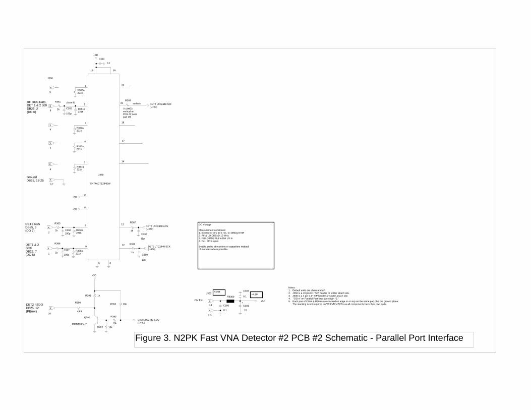
DET2 nCSDB25, 9(DO 7)
RF DDS Data,DET 1 & 2 SDIDB25, 2(DO 0)
DET2 nSDODB25, 12(PError)
Figure 3. N2PK Fast VNA Detector #2 PCB #2 Schematic - Parallel Port Interface
J360
C360
R360a221k
R361a221k
R369R361
C362
R362a221k
R363a221k
1k (0603 vertical on PCB #2 near pad 19)
R364a221k
U360
R365
C366 R365a221k
R367
C368
C369
R368
DET2 LTC2440 nCS(U460)
DET2 LTC2440 SCK(U460)
DET2 LTC2440 SDI(U460)
R366a221k
C367
R366DET1 & 2 SCKDB25, 7(DO 5)
R390
R391
R392
R393
R394
Q390Det2 LTC2440 SDO(U460)
J300FB300
C303
C301C300
Notes1. Default units are ohms and uF.2. J360 is a 10 pin 0.1" SIP header or solder attach site.3. J300 is a 4 pin 0.1" SIP header or solder attach site.4. "DO n" on Parallel Port lines are origin "0."5. Each pair of C36X & R36Xa are stacked on edge or on top on the same pad plus the ground plane. The stacking is not required on VE3IVM's PCBs as all components have their own pads.
X
X
X
X
X
X
8
10
Sig2
Sig1
32
VEE
8 1
+
3
4
1
14
1
2,3
+
6
Out1
12
Out2
+
-
+
18
+
MMBT3904-7
REF+
F0
IN-
IN+
4
2
7 6
3
2
6
7
4
+
-
3
2
7
4
+5V Det.
+5V Det.
LT1677CS8
6
0.1
+ +
5
1
40.1
49.9
1
2
2
1
2
6
4
6
4
1
T1-6T
T1-6T
0.01
10100.1
+12V Int.
+5V Det.
6,7
15p
47.5
49.9
49.9
0.1
2
10
10 10 10
1k
3
Gain1 Gain2
Car1
Car2
MC1496D
Bias
5
3.32k
0.1+12V Ext.
LT1677CS8
0.1
REF-
GND
VCC
0.1
3
49.9
10k
10k
0.1
2,3,
10
LM385M3-2.5
+12V Int.
1k0.1%(Note 5)
49.9
5
1k0.1%
5100.1%2.00k
0.1%
+3.109
-1.795
+5V Det
+0.663
+10.06
+4.99
+3.109
+3.109
+3.109
-4.96-9.68
DC Voltage
Measurement conditions:1. measured thru 10 k res. to 10Meg DVM2. RF & LO DDS @ 10 MHz3. Filt LO DDS Out to Det LO In4. Det. RF In open
Best to probe at resistors or capacitors instead of modules where possible.
short
14
0.01 0.01
100
100
LTC2440CGN
SDO
SCK
nCS
SDI
1,8,9,16
4
11
13
12
BUSY15
7
10
+2.493
3
5
6
0.1
2 6
4
LT1460ACS8-2.5
1000p(0402)
1000p(0402) 15p
(0603)
surface
2
nEXT
Det2 RF In(Front Panel -1.2V pp max. into 50 ohms)
Notes1. Default units are ohms and uF.2. J410 & J411 are 0.xxx" semi-rigid/braid coax solder attach site up to 0.125" dia. 3. J420 & J490 are 2 pin 0.1" SIP headers or solder attach sites.4. The on-board trace can NOT be used for Detector #2. DET2 LO IN at J410 is supplied from a suitable power splitter, such as the MCL PSC-2-1, and J180 which also feeds DET1 LO In at J210.5. All 0.1% resistors are 25 ppm/°C.6. Lifted pins, surface wiring, and 0402/0603 components are unique to mods for the original ExpressPCB PCB. VE3IVM's PCBs are designed for the fast detector and there is no need for lifted pins, surface wiring, or 0402/0603 components.
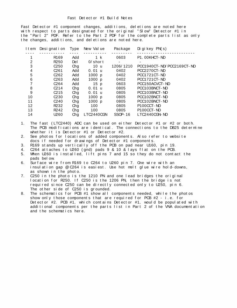
Fast Detector #1 Build Notes Fast Detector #1 component changes, additions, deletions are noted herewith respect to parts designated for the original "Slow" Detector #1 inthe "Part 2" PDF. Refer to the Part 2 PDF for the complete parts list as onlythe changes, additions, and deletions are noted here.
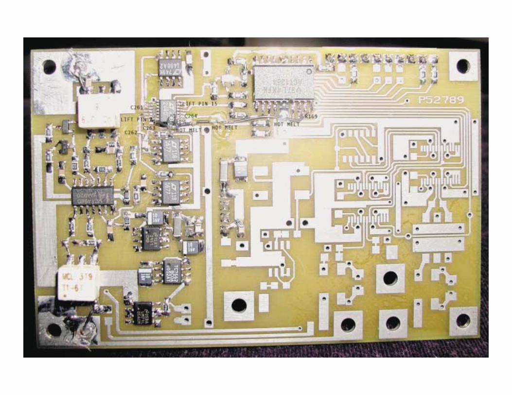
Item Designation Type New Value Package Digikey PN(s) ---- ----------- ---- ---------- --------- ------------------------- 1 R169 Add 1 k 0603 P1.00KHCT-ND 2 R250 Del 0/short - - 3 C250 Chg 10 u 1206/1210 PCC1940CT-ND/PCC2169CT-ND 4 C261 Add 0.01 u 0402 PCC2270CT-ND 5 C262 Add 1000 p 0402 PCC1721CT-ND 6 C263 Add 1000 p 0402 PCC1721CT-ND 7 C264 Add 15 p 0603 PCC150ACVCT-ND 8 C214 Chg 0.01 u 0805 PCC103BNCT-ND 9 C215 Chg 0.01 u 0805 PCC103BNCT-ND 10 C230 Chg 1000 p 0805 PCC102BNCT-ND 11 C240 Chg 1000 p 0805 PCC102BNCT-ND 12 R232 Chg 100 0805 P100CCT-ND 13 R242 Chg 100 0805 P100CCT-ND 14 U260 Chg LTC2440CGN SSOP-16 LTC2440CGN-ND 1. The fast (LTC2440) ADC can be used on either Detector #1 or #2 or both. The PCB modifications are identical. The connections to the DB25 determine whether it is Detector #1 or Detector #2.2. See photos for locations of added components. Also refer to website docs if needed for drawings of Detector #1 components.3. R169 stands up vertically off the PCB on pad near U160, pin 19.4. C264 attaches to U260 (gnd) pads 9 & 10 & lays flat on the PCB.5. When U260 is installed, lift pins 7 and 15 so they do not contact the pads below.6. Surface wire from R169 to C264 to U260 pin 7. One wire with an insulation gap @ C264 is easiest. Use hot melt glue wire hold-downs, as shown in the photo.7. C250 in the photo is the 1210 PN and one lead bridges the original location for R250. If C250 is the 1206 PN, then the bridge is not required since C250 can be directly connected only to U250, pin 6. The other side of C250 is grounded.8. The schematics for PCB #1 show all components needed, while the photos show only those components that are required for PCB #2 - i.e. for Detector #2. PCB #1, which contains Detector #1, would be populated with additional components per the parts list in Part 2 of the VNA documentation and the schematics here.
Fast Detector #2 Build Notes Fast Detector #2 component changes, additions, deletions are noted herewith respect to parts designated for the original "Slow" Detector #1 inthe "Part 2" PDF. The format here for Detector #2 under "Designation"is "new / old". A study of all schematics included here should make this clear.Refer to the Part 2 PDF for the complete parts list as only the changes, additions, and deletions are noted here.
Item Designation Type Value Package Digikey PN(s) ---- ----------- ---- ---------- --------- ------------------------- 1 R369 / R169 Add 1 k 0603 P1.00KHCT-ND 2 R450 / R250 Del 0 - - 3 C450 / C250 Chg 10 u 1206/1210 PCC1940CT-ND/PCC2169CT-ND 4 C461 / C261 Add 0.01 u 0402 PCC2270CT-ND 5 C462 / C262 Add 1000 p 0402 PCC1721CT-ND 6 C463 / C263 Add 1000 p 0402 PCC1721CT-ND 7 C464 / C264 Add 15 p 0603 PCC150ACVCT-ND 8 C414 / C214 Chg 0.01 u 0805 PCC103BNCT-ND 9 C415 / C215 Chg 0.01 u 0805 PCC103BNCT-ND 10 C430 / C230 Chg 1000 p 0805 PCC102BNCT-ND 11 C440 / C240 Chg 1000 p 0805 PCC102BNCT-ND 12 R432 / R232 Chg 100 0805 P100CCT-ND 13 R442 / R242 Chg 100 0805 P100CCT-ND 14 U460 / U260 Chg LTC2440CGN SSOP-16 LTC2440CGN-ND 1. The fast (LTC2440) ADC can be used on either Detector #1 or #2 or both. The PCB modifications are identical. The connections to the DB25 determine whether it is Detector #1 or Detector #2.2. See photos for locations of added components. Also refer to website docs if needed for drawings of Detector #1 components.3. R369 stands up vertically off the PCB on pad near U360, pin 19.4. C464 attaches to U460 (gnd) pads 9 & 10 & lays flat on the PCB.5. When U460 is installed, lift pins 7 and 15 so they do not contact the pads below.6. Surface wire from R369 to C464 to U460 pin 7. One wire with an insulation gap @ C464 is easiest. Use hot melt glue wire hold-downs, as shown in the photo.7. C450 in the photo is the 1210 PN and one lead bridges the original location for R450. If C450 is the 1206 PN, then the bridge is not required since C450 can be directly connected only to U450, pin 6. The other side of C450 is grounded.8. The schematics and photos show only those components that are required for Detector #2 PCB.
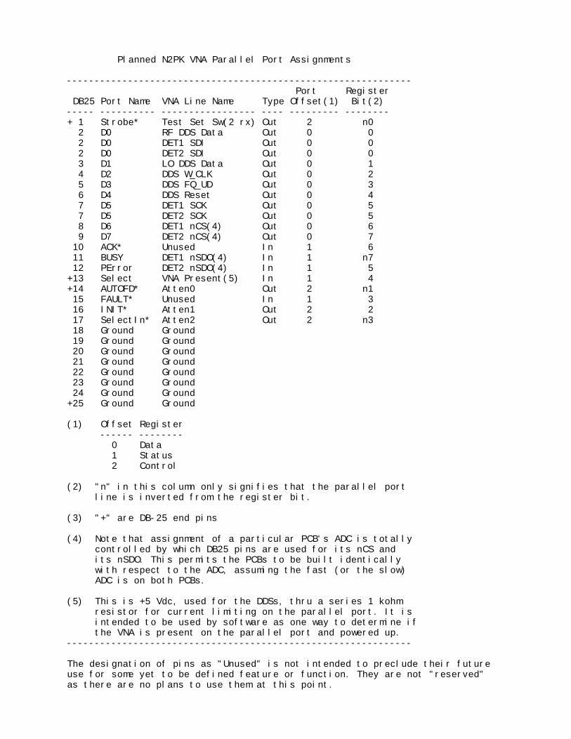
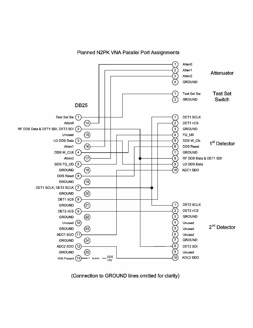
Planned N2PK VNA Parallel Port Assignments -------------------------------------------------------------- Port Register DB25 Port Name VNA Line Name Type Offset(1) Bit(2) ----- ---------- ----------------- ---- --------- -------- + 1 Strobe* Test Set Sw(2 rx) Out 2 n0 2 D0 RF DDS Data Out 0 0 2 D0 DET1 SDI Out 0 0 2 D0 DET2 SDI Out 0 0 3 D1 LO DDS Data Out 0 1 4 D2 DDS W_CLK Out 0 2 5 D3 DDS FQ_UD Out 0 3 6 D4 DDS Reset Out 0 4 7 D5 DET1 SCK Out 0 5 7 D5 DET2 SCK Out 0 5 8 D6 DET1 nCS(4) Out 0 6 9 D7 DET2 nCS(4) Out 0 7 10 ACK* Unused In 1 6 11 BUSY DET1 nSDO(4) In 1 n7 12 PError DET2 nSDO(4) In 1 5 +13 Select VNA Present(5) In 1 4 +14 AUTOFD* Atten0 Out 2 n1 15 FAULT* Unused In 1 3 16 INIT* Atten1 Out 2 2 17 SelectIn* Atten2 Out 2 n3 18 Ground Ground 19 Ground Ground 20 Ground Ground 21 Ground Ground 22 Ground Ground 23 Ground Ground 24 Ground Ground +25 Ground Ground (1) Offset Register ------ -------- 0 Data 1 Status 2 Control (2) "n" in this column only signifies that the parallel port line is inverted from the register bit. (3) "+" are DB-25 end pins
(4) Note that assignment of a particular PCB's ADC is totally controlled by which DB25 pins are used for its nCS and its nSDO. This permits the PCBs to be built identically with respect to the ADC, assuming the fast (or the slow) ADC is on both PCBs. (5) This is +5 Vdc, used for the DDSs, thru a series 1 kohm resistor for current limiting on the parallel port. It is intended to be used by software as one way to determine if the VNA is present on the parallel port and powered up. -------------------------------------------------------------- The designation of pins as "Unused" is not intended to preclude their futureuse for some yet to be defined feature or function. They are not "reserved"as there are no plans to use them at this point.
Detector #1 and Detector #2 LO Drive Options The original N2PK VNA has only one detector, while the Expanded N2PK VNA has two detectors. The LO DDS, via some combination ot its outputs at J180 and J120 must now drive the LO inputs of both detectors for proper VNA operation. Several options are possible. Here are three that come to mind: 1. Low loss 2-way power splitter from J180 to J210 and J410. A suitable power splitter for this is the MCL SCP-2-1. The splitter "S" port is driven by J180. This incurs approx. 3.2 dB loss over the original single detector configuration. With the lower 3 dB frequency of 100 kHz for the SCP-2-1, accuracy may suffer some at very low frequencies vs. the original configuration. Here is a picture of the SCP-2-1 splitter built by Harold, W4ZCB. A DOC file of the artwork can be made available on request.
2. Resistive power splitter from J180 to J210 and J410. Three 16 ohm resistors in a wye ("Y") configuration can be used. This incurs about 6 dB loss over the original configuration. However, little or no accuracy degradation would be expected over most of the frequency range. Between 50 and 60 MHz, there may be some accuracy loss due to the reduced LO drive. 3. Separate LO paths: J180 to J210 for Detector #1 and J120 through an added anti-alias filter to J410 for Detector #2. The added anti-alias filter components are identical to those currently used for the J180 output. The new anti-alias filter should not be jury-rigged onto PCB #1 due to coupling between the filter and the near-by RF DDS components. The VE3IVM dual detector PCBs have the anti-alias filter components present for the J120 LO DDS Output.
This option provides essentially the same LO drive levels to each detector as the original configuration, so there should be no loss in accuracy due to drive level. However, for the original ExpressPCB PCBs coupling at 28 MHz from the RF DDS to J120 is 16 dB higher than the coupling from the RF DDS to J180. At 28 MHz, the RF DDS signal at J180 is approx. 72 dB down from the LO DDS level. At 14 MHz, it's about 6 dB lower so I'd expect it to be about 6 dB worse at 56 MHz. Likely most of the coupling is capacitive which would make the slope 6 dB/octave. For the VE3IVM PCBs, the isolation between DDS outputs is somewhat better than for the ExpressPCB PCB. Currently I am using either option 1 or option 2 with ExpressPCB PCBs. Originally, it was recommended that the LO paths be made via VNA front panel coaxial jumpers to permit the optional use of attenuators for improvements to undesired harmonic mixing, where needed, as noted at: http://n2pk.com/TestResult6.html However, now with “Harmonic Suppression” as described in posts at the N2PK-VNA Yahoogroup, undesired harmonic mixing is virtually eliminated in fundamental mode.


![Painting recognition from wearable cameras · ORB ([16]) is short for Oriented FAST and Rotated BRIEF. The keypoint detector uses FAST ([15]), a corner detector, combined with a Harris](https://static.documents.pub/doc/80x56/5fa02e817664eb5a7d7cdf88/painting-recognition-from-wearable-cameras-orb-16-is-short-for-oriented-fast.jpg)


